EP1560322A1 - Verfahren zur Betätigung eines Schalters in einem Wandlerstufe eines mehrphasigen DC-Spannungswandlers, und der mehrphasige DC-Spannungswandler - Google Patents
Verfahren zur Betätigung eines Schalters in einem Wandlerstufe eines mehrphasigen DC-Spannungswandlers, und der mehrphasige DC-Spannungswandler Download PDFInfo
- Publication number
- EP1560322A1 EP1560322A1 EP04001673A EP04001673A EP1560322A1 EP 1560322 A1 EP1560322 A1 EP 1560322A1 EP 04001673 A EP04001673 A EP 04001673A EP 04001673 A EP04001673 A EP 04001673A EP 1560322 A1 EP1560322 A1 EP 1560322A1
- Authority
- EP
- European Patent Office
- Prior art keywords
- signal
- control signal
- current
- actuation
- output
- Prior art date
- Legal status (The legal status is an assumption and is not a legal conclusion. Google has not performed a legal analysis and makes no representation as to the accuracy of the status listed.)
- Withdrawn
Links
Images


Classifications
-
- H—ELECTRICITY
- H02—GENERATION; CONVERSION OR DISTRIBUTION OF ELECTRIC POWER
- H02M—APPARATUS FOR CONVERSION BETWEEN AC AND AC, BETWEEN AC AND DC, OR BETWEEN DC AND DC, AND FOR USE WITH MAINS OR SIMILAR POWER SUPPLY SYSTEMS; CONVERSION OF DC OR AC INPUT POWER INTO SURGE OUTPUT POWER; CONTROL OR REGULATION THEREOF
- H02M3/00—Conversion of DC power input into DC power output
- H02M3/02—Conversion of DC power input into DC power output without intermediate conversion into AC
- H02M3/04—Conversion of DC power input into DC power output without intermediate conversion into AC by static converters
- H02M3/10—Conversion of DC power input into DC power output without intermediate conversion into AC by static converters using discharge tubes with control electrode or semiconductor devices with control electrode
- H02M3/145—Conversion of DC power input into DC power output without intermediate conversion into AC by static converters using discharge tubes with control electrode or semiconductor devices with control electrode using devices of a triode or transistor type requiring continuous application of a control signal
- H02M3/155—Conversion of DC power input into DC power output without intermediate conversion into AC by static converters using discharge tubes with control electrode or semiconductor devices with control electrode using devices of a triode or transistor type requiring continuous application of a control signal using semiconductor devices only
- H02M3/156—Conversion of DC power input into DC power output without intermediate conversion into AC by static converters using discharge tubes with control electrode or semiconductor devices with control electrode using devices of a triode or transistor type requiring continuous application of a control signal using semiconductor devices only with automatic control of output voltage or current, e.g. switching regulators
- H02M3/158—Conversion of DC power input into DC power output without intermediate conversion into AC by static converters using discharge tubes with control electrode or semiconductor devices with control electrode using devices of a triode or transistor type requiring continuous application of a control signal using semiconductor devices only with automatic control of output voltage or current, e.g. switching regulators including plural semiconductor devices as final control devices for a single load
- H02M3/1584—Conversion of DC power input into DC power output without intermediate conversion into AC by static converters using discharge tubes with control electrode or semiconductor devices with control electrode using devices of a triode or transistor type requiring continuous application of a control signal using semiconductor devices only with automatic control of output voltage or current, e.g. switching regulators including plural semiconductor devices as final control devices for a single load with a plurality of power processing stages connected in parallel
-
- H—ELECTRICITY
- H02—GENERATION; CONVERSION OR DISTRIBUTION OF ELECTRIC POWER
- H02J—ELECTRIC POWER NETWORKS; CIRCUIT ARRANGEMENTS OR SYSTEMS FOR SUPPLYING OR DISTRIBUTING ELECTRIC POWER; SYSTEMS FOR STORING ELECTRIC ENERGY
- H02J1/00—Circuit arrangements for DC mains or DC distribution networks
- H02J1/10—Parallel operation of DC sources
- H02J1/102—Parallel operation of DC sources being switching converters
Definitions
- the present invention relates to a method for actuating a switch in a transformer stage of a multiphase DC voltage transformer (or multiphase DC to DC converter) and a multiphase DC voltage transformer.
- Such DC voltage transformers contain several individual transformer stages, which are switched in parallel with the voltage or current source of a load.
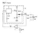
- the transformer stage 31 puts out across an output terminal K10 an output current Iout1 to a rectifying capacitor Cout1 and a load switched in parallel with the capacitor Cout1.
- an automatic controller 11 produces a control signal S11 from the difference between the output voltage Vout1, or a signal dependent thereon, and a reference signal Vref1.
- the controller 11 is designed for example as an integral controller or a proportional-integral controller.
- the control signal S11 is fed to an actuator unit 21 in the transformer stage 31, which provides an actuating signal S21 for a switch SW10, which is connected in series with an inductive storage element L1 between one terminal for an input voltage Vin1 and the output terminal K10.
- a diode D1 connected between a reference potential GND1 and the coil L1 serves as a free-wheeling element for the inductive storage element L1 when the switch SW10 is open.
- the actuating circuit 21 is fed a current metering signal S41, which is proportional to the output current Iout1, and a clock signal CLK1, in addition to the voltage control signal S11.
- the output current Iout1 rises linearly across the inductance L1, and the rise in this current is dependent on the difference between the input voltage Vin1 and the output voltage Vout1 and the inductivity value of the inductance L1.
- this output current Iout1 decreases linearly.
- the duration of the individual turn-on pulses or the duty cycle of the actuator signal S21 is dependent on the voltage control signal S11, in order to achieve control of the output voltage Vout1 via the voltage control signal S11.
- the switch SW10 for example, is opened in the clock pulse of the clock signal CLK1 and then closed whenever the current metering signal S41 has decreased to the value of the first control signal S11.
- the mean current delivery with this method is proportional to the mean value S41m of the current metering signal S41, while in the steady-state condition this mean value S41m corresponds to the voltage control signal S11 plus an offset. This offset corresponds, for the triangular current operation shown, to half of the signal deviation of the current metering signal S41.
- a voltage controller is available, corresponding to the voltage controller 11 in Figure 1, and its control signal is provided to the individual transformer stages.
- the overall output current of the multiphase transformer and the number of transformer stages switched in parallel is used to determine an average output current and this is compared with the particular output currents of the individual transformer stages. If the output current of a transformer stage is greater than this average current, then the duty cycle of the actuation signal is decreased in this transformer stage in order to reduce the current delivery of this transformer stage. If the current delivery of a transformer stage is too small compared to the average current, then the duty cycle of the particular transformer stage is increased.
- one transformer stage is defined as the reference stage (master), whose output current serves as the reference current for the other transformer stages(slaves).
- the duty cycle of the actuation signals in the other transformer stages is then adjusted so that the output currents of these transformer stages correspond to the reference current.
- the goal of the present invention is to provide a method for actuating a switch in a transformer stage of a multiphase DC voltage transformer and a multiphase DC voltage transformer in which a uniform current loading of the individual transformer stages is ensured.
- the method involves the actuation of a switch which controls the current uptake in one of at least two parallel switched transformer stages of a multiphase DC voltage transformer, which has an output terminal for connecting a load and for making available an output voltage for the load from an input voltage.
- the method involves providing a first control signal, which is dependent on the output voltage, as well as a current metering signal which is at least temporarily dependent on an output current of the transformer stage, and providing from the first control signal and the current metering signal an actuation signal having a sequence of actuation pulses, whose duty cycle depending on the first control signal and the current metering signal is automatically controlled to a value at which the mean value of the output current is proportional to the first control signal.
- the duty cycle of the actuation signal is controlled, depending on the first control signal and the current metering signal, to a value at which the mean value of the current control signal corresponds to the first control signal.
- the control of the current uptake of the individual transformer stages of a multiphase DC voltage transformer is thus, in this method, dependent on the first control signal that regulates the output voltage, and by regulating the mean value of the output current in proportion to the first control signal one ensures that the individual transformer stages contribute an identical amount to the overall current, regardless of manufacturing-related variances in the inductivity values of the inductive storage elements, and the resulting different steepnesses of the slopes of the output current diagram.
- the proportionality factor between the first control signal and the mean value of the output current is the same for all transformer stages, so as to achieve an identical current loading of the transformer stages.
- the multiphase DC voltage transformer contains an output terminal for furnishing an output voltage from an input voltage, a first controller for furnishing a first control signal dependent on the output voltage, and at least two transformer stages.
- the transformer stages each contain an inductive energy storage element coupled to the output terminal, a switch which controls the current uptake of the inductive energy storage element and which is actuated in accordance with an actuation signal, and a current metering arrangement to furnish a current metering signal dependent on an output current.
- the individual transformer stages furthermore, each contain an actuation circuit, which receives the first control signal and the current metering signal and furnishes the actuation signal for the at least one switch, wherein the actuation circuit controls the duty cycle of the actuation signal to a value at which the mean value of the output current is proportional to the first control signal.
- the actuation circuit is designed to control the duty cycle of the actuation signal to a value at which the mean value of the current metering signal corresponds to the first control signal.
- the actuation circuit contains, for example, a pulse width modulator, to which the current metering signal and a difference signal formed from the first control signal and a second control signal are sent, a second control arrangement, to which the first control signal and the current metering signal are sent, and which furnishes the second control signal, and a subtractor, which furnishes the diffference signal from the first control signal and the second control signal.
- a pulse width modulator to which the current metering signal and a difference signal formed from the first control signal and a second control signal are sent
- a second control arrangement to which the first control signal and the current metering signal are sent, and which furnishes the second control signal
- a subtractor which furnishes the diffference signal from the first control signal and the second control signal.
- Figure 3 shows a multiphase DC voltage transformer, which has an output terminal OUT to furnish an at least approximately load-independent output voltage Vout for a load that can be connected to the output terminal OUT.
- An output capacitor Cout switched in parallel with the load is used to smooth the furnished output voltage Vout.
- the controlling of the output voltage Vout is effected in terms of the output current Iout delivered across the multiphase DC voltage transformer.
- the DC voltage transformer contains several transformer stages 2_1, 2_n (in the present case, two), each of which is furnished an input voltage Vin, and each having outputs K1, Kn connected to the output terminal OUT, at each of which is furnished a partial current Iout_1, Iout_n of the overall current Iout.
- a first controller 1 For controlling the output voltage Vout via the output current Iout or the partial currents Iout_1, Iout_n of the individual transformer stages 2_1, 2_n there is provided a first controller 1, which compares the output voltage Vout or a metering signal dependent thereon with a reference value Vref and which furnishes a first control signal S1, which is fed to the individual transformer stages 2_1, 2_n.
- the controller 1 is configured, for example, as a conventional proportional-integral controller or as an integral controller.
- the reference voltage Vref assigns the nominal value to which the output voltage Vout is regulated.
- FIG. 4 shows a circuitry sample embodiment for the individual transformer stages 2_1, 2_n.
- Figure 4 shows the load, the output capacitor Cout, and the controller 1 which furnishes the first control signal S1, in addition to the transformer stage.
- the transformer stage of Figure 4 is designed as a stepdown device, which has a series circuit of a switch SW and an inductive storage element L between a terminal for the input voltage Vin and the output terminal K1, Kn of the transformer stage 2_1, 2_n.
- the load in the sample embodiment is switched between the output terminal K1, Kn and the reference potential GND. Between this reference potential GND and a junction shared by the switch SW and the inductance L there is switched a free-wheeling element, in the present case a diode D, which takes over the current through the inductance L when the switch SW is blocked.
- the transformer stage 2 contains a current metering arrangement 4 for detecting the output current Iout and for furnishing a current metering signal S4 proportional to this output current Iout.
- the switch SW is clocked according to an actuation signal S3 furnished by an actuation circuit.
- This actuation circuit is configured so as to control the duty cycle of the actuation signal S3 to a value at which the mean value of the output current Iout is proportional to the first control signal S1 or at which a mean value of the current metering signal S4 corresponds to the first control signal S1.
- the actuation circuit contains a pulse width modulator 3, to whose output the actuation signal S3 is furnished, and to which the current metering signal S4 as well as a difference signal S6 from the first control signal S1 and a second control signal S5 is furnished.
- the difference signal S6 is furnished at the output of a subtractor 6, to which the first control signal S1 and the second control signal S5 are furnished.
- the second control signal S5 is furnished at the output of a second controller arrangement 5, to which the first control signal S1 and the current metering signal S4 are furnished.
- the pulse width modulator 3 shown in Figure 4 is designed to open the switch SW, timed by a clock signal CLK, and then to close it when the current metering signal S4 has dropped to the value of the difference signal S6.
- the pulse width modulator 3 contains a comparator 31, to one input of which is supplied the difference signal S6 and to its other input the current metering signal S4.
- a comparator output signal S31 is supplied to a set input of an RS flip-flop 32, at whose non-inverting output Q the actuation signal S3 for the switch SW is provided.
- the clock signal CLK is furnished to the reset input of this flip-flop 32, in order to open the switch SW in time with this clock signal CLK.
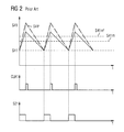
- Figure 5 illustrates, as an example, the diagram of the current metering signal S4, which is proportional to the output current Iout, as a function of the clock signal CLK and the comparator output signal S31 or the difference signal S6.
- the switch SW is closed after a rising edge of the comparator output signal S31, the output current Iout and, with it, the current metering signal S4, rises linearly until the switch SW timed by the clock signal CLK is turned off.
- the output current Iout or the current metering signal S4 then decreases linearly until the current metering signal S4 reaches the value of the difference signal S6, again turning the switch SW on.
- the current diagram is triangular in shape.
- the mean value of the current metering signal S4 is automatically controlled to the value of the first control signal S1, regardless of the inductivity values of the inductances L used in the individual transformer stages and regardless of the different input voltages Vin of the individual transformer stages, if so desired.
- S4' represents the time course of the current metering signal for a changed inductivity value and/or a changed input voltage Vin.
- the deviation in level of the current metering signal S4' in this case is greater than that of the already discussed current metering signal S4, from which the second control arrangement 5 produces a difference signal S6' which is smaller than the difference signal S6, but which likewise makes the mean value of the current metering signal S4' correspond to the first control signal S1.
- the method of the invention assures - when the duty cycle of the actuation signal S3 is adjusted so that the mean value of the current metering signal corresponds to the first control signal S1 - that all the transformer stages contribute the same partial currents to the output current.
- the first control signal S1 which is present in any case, and the current metering signal S4 produced in the transformer stages, no other signals need be furnished to the individual transformer stages.
- the second automatic control arrangement 5 can be deactivated in the beginning, for example.
- the beginning of the actuation pulse of the actuation signal S3 then occurs as a function of the current metering signal S4 and the first control signal S1, which in this case is at first identical to the difference signal S6. If the control arrangement 5 is then turned on, the difference signal S6 will be decreased until the mean value of the current metering signal S4 corresponds to the first control signal S1. Decreasing the difference signal S6 will produce (referring to Figure 5) a decrease in the mean current uptake, which is opposed by way of an increase in the first control signal S1.
- a sample embodiment of a second control arrangement 5 is shown in Figure 6a.
- the control arrangement has as its integrating element 56 a capacitor, to which is connected a charging circuit 51, 52 as well as a discharging circuit 53, 54.
- the charging circuit in the sample embodiment, comprises a series connection of a current source 51 and a switch 52 between a power supply potential V1 and a lead of the capacitor 56 opposite the reference potential GND.
- the discharging circuit comprises a series connection of a second current source 53 and a second switch 54 between reference potential GND and the lead of the capacitor 56 opposite the reference potential GND.
- the charging and discharging circuits are actuated in complementary fashion to each other as determined by a comparison signal S58.
- the comparison signal S58 is furnished directly to the switch 52 of the charging circuit 51, 52 and across an inverter 55 to the switch 54 of the discharging circuit 53, 54.
- the comparison signal S58 is produced by means of a comparator 58 from the first control signal S1 and the current metering signal S4.
- these signals S1, S4 are current signals, and these current signals with different sign are impressed on a circuit branch point, which is connected across a resistor 59 to reference potential GND.
- a comparator 58 compares the voltage across this resistor 59 to the reference potential in order to provide the comparison signal S58.
- the comparator signal S58 has a high level, in order to charge the capacitor 56 with the current furnished from the first current source 51, when the current metering signal S4 is larger than the first control signal S1. If the first control signal S1 is larger than the current metering signal S4, the capacitor 56 will be discharged across the discharge circuit 53, 54. A voltage V56 across the capacitor 56 is amplified by means of an amplifier 57, while the second control signal S5 is present at the output of this amplifier 57. Each of the currents delivered by the current sources 51, 53 are the same.
- Figure 6b shows, for the duration of an actuation period of the switch SW, the time variation of the current metering signal S4, as well as the variation of the voltage V56 across the capacitor 56, or the second control signal S5.
- the first control signal S1 in the sample embodiment is larger than the minimum value of the current metering signal S4 but smaller than the mean value S4m of the current metering signal S4.
- the capacitor 56 will at first be discharged until the current metering signal S4 reaches the value of the first control signal S1.
- the capacitor will discharge until such time as the value of the current metering signal S4 has again dropped below the value of the first control signal S1.
- the charging time of the capacitor 56 is larger than the discharging time, so that at the end of the actuation period there results a higher instantaneous value for the second control signal S5.
- a second rising control signal results in a diminishing difference signal S6, which results in a decreased mean current uptake, in order to bring the mean value S4m of the current metering signal S4 closer to the first control signal S1, until the adjusted state depicted in Figure 5 is achieved, at which the mean value S4m of the current metering signal corresponds to the first control signal S1.
- the charging time of the capacitor 56 corresponds to its discharging time, so that the value of the second control signal S5 at the start of an actuation period corresponds to the value at the end of the actuation period, which is equivalent to the mean value of the second control signal S5 remaining the same.
- a sample-and-hold element is preferably connected to the amplifier 57 in a way not otherwise specified, which samples the second control signal S5 each time in synchronization with the clock signal CLK, in order to hold the value of the control signal S5 constant for the next actuation period each time.
- FIG. 7a shows a modification of the second control arrangement depicted in Figure 6a.
- This control arrangement shown in Figure 7a, contains a release circuit with AND gates 61, 62, to one input each of which is furnished the actuation signal S2 inverted by means of an inverter 60.
- To the other input of one of the gates 61 is furnished the comparison signal 58 and to the other input of the other gate 62 is furnished the inverted comparison signal.
- the outputs of the gates 61, 62 actuate the switches 52, 53 of the charging and discharging circuits.
- the release circuit 60, 61, 62 ensures that an evaluation of the current metering signal S4 in relation to the first control signal S1 only takes place during periods of time when the switch SW is turned off.
- Figure 7b shows, for this control arrangement, the time variation of the second control signal S5 as a function of the current metering signal S4, the first control signal S1, and the actuation signal S3.
- Charging of the capacitor 56 in this sample embodiment only occurs during a falling edge of the current metering signal S4, thus, while the switch SW is shut off. The capacitor is charged until the current metering signal S4 is greater than the first control signal S1, and thereafter it is discharged.
- the second control signal S5 maintains a constant value.
- FIG. 8 Another sample embodiment of a second control arrangement is shown in Figure 8.
- This control arrangement contains a subtractor 63, to which the current metering signal S4 and the first control signal S1 are sent, and which provides a current signal S63, dependent on the difference between the current metering signal S4 and the first control signal S1, that is sent to the capacitor 56.
- the voltage V56 across the capacitor 56 increases for as long as the current metering signal S4 is larger than the first control signal S1, and it decreases when the first control signal S1 is larger than the current metering signal S4.
- the steepness with which the voltage increase or decrease occurs is dependent on the difference between the current metering signal S4 and the first control signal S1.
- the voltage V56 across the capacitor 56 is amplified by means of an amplifier 57, in order to provide the second control signal S5.
- FIG 9 shows a modification of the transformer stage shown in Figure 4.
- the first switch is configured as a MOSFET T1, to which the output signal S3 of the actuation circuit 3 is sent across a driver circuit 21.
- the free-wheeling element between the inductance L and reference potential GND is likewise formed by a MOSFET T2 in this sample embodiment, which is actuated in complementary fashion to the first switch T1.
- the signal at the inverting output Q' of the RS flip-flop 32 is sent to this second MOSFET T2 across a driver circuit 22.
- the current metering signal S4 in this sample embodiment is furnished by a measuring amplifier 4, whose input terminals are connected to the load pins of the second MOSFET T2, in order to detect, when the first MOSFET T1 is blocked, the free-wheeling current flowing across the second MOSFET T2, which corresponds to the output current Iout when the first MOSFET T1 is switched off.
- the second control arrangement 5 in this sample embodiment is preferably configured according to the control arrangement shown in Figure 7a, which only determines the second control signal S5 during shut-off periods of the first switch T1, controlling the current uptake.
Landscapes
- Engineering & Computer Science (AREA)
- Power Engineering (AREA)
- Dc-Dc Converters (AREA)
Priority Applications (1)
| Application Number | Priority Date | Filing Date | Title |
|---|---|---|---|
| EP04001673A EP1560322A1 (de) | 2004-01-27 | 2004-01-27 | Verfahren zur Betätigung eines Schalters in einem Wandlerstufe eines mehrphasigen DC-Spannungswandlers, und der mehrphasige DC-Spannungswandler |
Applications Claiming Priority (1)
| Application Number | Priority Date | Filing Date | Title |
|---|---|---|---|
| EP04001673A EP1560322A1 (de) | 2004-01-27 | 2004-01-27 | Verfahren zur Betätigung eines Schalters in einem Wandlerstufe eines mehrphasigen DC-Spannungswandlers, und der mehrphasige DC-Spannungswandler |
Publications (1)
| Publication Number | Publication Date |
|---|---|
| EP1560322A1 true EP1560322A1 (de) | 2005-08-03 |
Family
ID=34639379
Family Applications (1)
| Application Number | Title | Priority Date | Filing Date |
|---|---|---|---|
| EP04001673A Withdrawn EP1560322A1 (de) | 2004-01-27 | 2004-01-27 | Verfahren zur Betätigung eines Schalters in einem Wandlerstufe eines mehrphasigen DC-Spannungswandlers, und der mehrphasige DC-Spannungswandler |
Country Status (1)
| Country | Link |
|---|---|
| EP (1) | EP1560322A1 (de) |
Cited By (1)
| Publication number | Priority date | Publication date | Assignee | Title |
|---|---|---|---|---|
| CN102548125A (zh) * | 2010-11-16 | 2012-07-04 | 黑拉许克联合股份有限公司 | 发光二极管的馈电电路装置 |
Citations (2)
| Publication number | Priority date | Publication date | Assignee | Title |
|---|---|---|---|---|
| US6433527B1 (en) * | 2001-06-01 | 2002-08-13 | Maxim Integrated Products, Inc. | Phase failure detector for multi-phase switching regulators |
| WO2003103119A1 (en) * | 2002-06-04 | 2003-12-11 | Koninklijke Philips Electronics N.V. | Dc-dc converter |
-
2004
- 2004-01-27 EP EP04001673A patent/EP1560322A1/de not_active Withdrawn
Patent Citations (2)
| Publication number | Priority date | Publication date | Assignee | Title |
|---|---|---|---|---|
| US6433527B1 (en) * | 2001-06-01 | 2002-08-13 | Maxim Integrated Products, Inc. | Phase failure detector for multi-phase switching regulators |
| WO2003103119A1 (en) * | 2002-06-04 | 2003-12-11 | Koninklijke Philips Electronics N.V. | Dc-dc converter |
Cited By (2)
| Publication number | Priority date | Publication date | Assignee | Title |
|---|---|---|---|---|
| CN102548125A (zh) * | 2010-11-16 | 2012-07-04 | 黑拉许克联合股份有限公司 | 发光二极管的馈电电路装置 |
| CN102548125B (zh) * | 2010-11-16 | 2016-03-16 | 黑拉许克联合股份有限公司 | 用于对负载馈电的电路装置和方法 |
Similar Documents
| Publication | Publication Date | Title |
|---|---|---|
| CN102084581B (zh) | 单电感多输出转换器 | |
| JP3981110B2 (ja) | マルチ位相合成リプル電圧レギュレータの同期 | |
| US8890501B2 (en) | System and method for soft-starting a power converter with a pre-charged output | |
| CN112689947B (zh) | 四开关、单电感器、非反相的降压-升压转换器的控制 | |
| US10181792B2 (en) | Sensor-less buck current regulator with average current mode control | |
| US7583133B2 (en) | Self-oscillating regulated low-ripple charge pump and method | |
| US5973944A (en) | Inductorless step-up and step-down converter with inrush current limiting | |
| US7777457B2 (en) | Constant frequency current-mode buck-boost converter with reduced current sensing | |
| EP1691473B1 (de) | Schnell ansprechender, Zweirampensignale verwendender PWM-Regler mit Zweiflankenmodulation | |
| US8080987B1 (en) | Method and apparatus for efficient transitioning between different operating modes of a regulator | |
| US7795761B2 (en) | Power converters with switched capacitor buck/boost | |
| US10044267B1 (en) | Current emulation auto-calibration with peak-current servo | |
| CN102882371A (zh) | 用于降压-升压转换器的高效率pfm控制 | |
| US9819264B1 (en) | Controller for a power converter | |
| US11005372B2 (en) | Two-stage multi-phase switching power supply with ramp generator DC offset for enhanced transient response | |
| EP1804368A1 (de) | Methode zur Gleichstromwandlung and Gleichstromwandleranordnung | |
| CN112311236A (zh) | 开关模式电源 | |
| US20080224681A1 (en) | Controller for a DC to DC Converter | |
| US10234881B1 (en) | Digitally-assisted capless voltage regulator | |
| CN101546957B (zh) | 含控制器的直流/直流转换器及其控制方法 | |
| US12199511B2 (en) | Voltage converter having adjustable phases | |
| EP1560322A1 (de) | Verfahren zur Betätigung eines Schalters in einem Wandlerstufe eines mehrphasigen DC-Spannungswandlers, und der mehrphasige DC-Spannungswandler | |
| US12301096B2 (en) | Constant ripple algorithm in DCM for buck converter | |
| US20230223852A1 (en) | Dc-dc converter and method of operating the same | |
| US10389250B1 (en) | Operating mode for a DC-DC converter to obtain a broad range of output voltages |
Legal Events
| Date | Code | Title | Description |
|---|---|---|---|
| PUAI | Public reference made under article 153(3) epc to a published international application that has entered the european phase |
Free format text: ORIGINAL CODE: 0009012 |
|
| AK | Designated contracting states |
Kind code of ref document: A1 Designated state(s): AT BE BG CH CY CZ DE DK EE ES FI FR GB GR HU IE IT LI LU MC NL PT RO SE SI SK TR |
|
| AX | Request for extension of the european patent |
Extension state: AL LT LV MK |
|
| 17P | Request for examination filed |
Effective date: 20050706 |
|
| AKX | Designation fees paid |
Designated state(s): DE FR IT |
|
| 17Q | First examination report despatched |
Effective date: 20070109 |
|
| RAP1 | Party data changed (applicant data changed or rights of an application transferred) |
Owner name: INFINEON TECHNOLOGIES AG |
|
| STAA | Information on the status of an ep patent application or granted ep patent |
Free format text: STATUS: THE APPLICATION IS DEEMED TO BE WITHDRAWN |
|
| 18D | Application deemed to be withdrawn |
Effective date: 20100716 |