EP1582350A1 - Sensor unit and print state inspection apparatus using the same - Google Patents

Sensor unit and print state inspection apparatus using the same Download PDF

Info

Publication number
EP1582350A1
EP1582350A1 EP05006590A EP05006590A EP1582350A1 EP 1582350 A1 EP1582350 A1 EP 1582350A1 EP 05006590 A EP05006590 A EP 05006590A EP 05006590 A EP05006590 A EP 05006590A EP 1582350 A1 EP1582350 A1 EP 1582350A1
Authority
EP
European Patent Office
Prior art keywords
print
light
sensor unit
print surface
image pickup
Prior art date
Legal status (The legal status is an assumption and is not a legal conclusion. Google has not performed a legal analysis and makes no representation as to the accuracy of the status listed.)
Withdrawn
Application number
EP05006590A
Other languages
German (de)
French (fr)
Inventor
Mamoru Sawamura
Current Assignee (The listed assignees may be inaccurate. Google has not performed a legal analysis and makes no representation or warranty as to the accuracy of the list.)
Aan Corp Co Ltd
Original Assignee
Aan Corp Co Ltd
Priority date (The priority date is an assumption and is not a legal conclusion. Google has not performed a legal analysis and makes no representation as to the accuracy of the date listed.)
Filing date
Publication date
Application filed by Aan Corp Co Ltd filed Critical Aan Corp Co Ltd
Publication of EP1582350A1 publication Critical patent/EP1582350A1/en
Withdrawn legal-status Critical Current

Links

Images

Classifications

    • BPERFORMING OPERATIONS; TRANSPORTING
    • B41PRINTING; LINING MACHINES; TYPEWRITERS; STAMPS
    • B41FPRINTING MACHINES OR PRESSES
    • B41F33/00Indicating, counting, warning, control or safety devices
    • B41F33/0036Devices for scanning or checking the printed matter for quality control

Definitions

  • the present invention relates to a sensor unit and a print state inspection apparatus using the sensor unit. More specifically, the present invention relates to a sensor unit, which is highly accurate and whose miniaturization is possible, and a print state inspection apparatus using the sensor unit.
  • a print state inspection apparatus which irradiates a print surface with light, picks up an image formed by reflected light from the print surface, and detects a print defect with reference to the obtained image.
  • FIG. 7 is a schematic construction diagram of an example of a conventional print state inspection apparatus.
  • a print state inspection apparatus 700 shown in FIG. 7 is an inspection apparatus of so-called in-line type and continuously inspects print surfaces of prints transported. To do so, the apparatus 700 includes a sensor portion 710 and a print transport portion 720 .
  • the sensor portion 710 includes an image pickup element 71 and an illumination means 72 .
  • the illumination means 72 irradiates a print surface of a print W supplied to the transport portion with light, the image pickup element 71 captures an image formed by reflected light from the print surface, and a detection portion (not shown) detects a print defect by analyzing image data of the image.
  • the image pickup element 71 is preferably a CCD camera because it is possible to achieve high accuracy with the CCD camera.
  • a distance between the CCD camera 71 and the print W becomes very long (ordinarily, a distance of 800 mm or more is required). Therefore, it is required to incorporate the sensor portion 710 into a print apparatus from an early stage of manufacture, which makes it impossible to commercialize the sensor portion alone. Also, when it is desired to improve the inspection accuracy of the print apparatus, it is required to modify or change an inspection apparatus incorporated into the print apparatus, which is very disadvantageous in terms of economy.
  • a sensor unit which is highly accurate and whose miniaturization is possible, and a print state inspection apparatus using the sensor unit are strongly desired.
  • the present invention has been made in order to solve the above-mentioned problems with the prior art, and has an object to provide a sensor unit, which is highly accurate and whose miniaturization is possible, and a print state inspection apparatus using the sensor unit.
  • a sensor unit irradiates a print surface with light and picks up an image formed by reflected light from the print surface.
  • the sensor unit comprises: an image pickup portion including an image pickup element and a lens fitted to the image pickup element; an illumination portion including a light-emission element and a lens fitted to the light-emission element; and a reflecting portion including at least one mirror that reflects the reflected light from the print surface in a direction having a predetermined angle with respect to a direction of normal to the print surface.
  • the reflecting portion includes: a first mirror that reflects the reflected light from the print surface in a first direction having a predetermined angle with respect to the direction of the normal to the print surface; and a second mirror that reflects the light reflected in the first direction in a second direction having a predetermined angle with respect to the first direction.
  • the first direction has an angle of 90 degrees with respect to the direction of the normal to the print surface
  • the second direction has an angle of 90 degrees with respect to the first direction
  • the image pickup element is a CCD camera
  • the light-emission element is a high-intensity LED
  • the first mirror and the second mirror are each an evaporated mirror.
  • a print state inspection apparatus irradiates a print surface of a print arranged at a predetermined position with light, picks up an image formed by reflected light from the print surface, and detects a print defect with reference to an obtained image.
  • the print state inspection apparatus comprises: a sensor portion that irradiates the print surface with the light and picks up the image formed by the reflected light from the print surface; and a detection portion that detects the print defect by analyzing image data obtained by the sensor portion, wherein the sensor portion includes: an image pickup portion including an image pickup element and a lens fitted to the image pickup element; an illumination portion including a light-emission element and a lens fitted to the light-emission element; and a reflecting portion including at least one mirror that reflects the reflected light from the print surface in a direction having a predetermined angle with respect to a direction of normal to the print surface.
  • a specific light-emission element is combined with an optical systemas an illumination portion, and a reflecting portion that uses a specific mirror is provided.
  • a sensor unit which is highly accurate and whose miniaturization is possible, and a print state inspection apparatus using the sensor unit.
  • the sensor unit of the present invention it is possible to reduce the height of the unit to around 220 mm.
  • a working distance distance between a sensor lower end (in the vicinity of an illumination portion) and a print
  • FIG. 1 is a schematic construction diagram of a sensor unit according to a preferred embodiment of the present invention
  • FIG. 2 is a schematic perspective view illustrating an entire external appearance of the sensor unit shown in FIG. 1
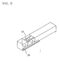
  • FIG. 3 is a see-through schematic perspective view illustrating a state of an image pickup portion in the sensor unit.
  • a sensor unit 100 is a unit that irradiates a print surface of a print W with light and picks up an image formed by reflected light from the print surface. To do so, the sensor unit 100 includes an image pickup portion 10 , an illumination portion 20 , and a reflecting portion 30.
  • the image pickup portion 10 includes an image pickup element 11 and a lens 12 fitted to the image pickup element 11 .
  • the illumination portion 20 includes a light-emission element 21 and a lens 22 fitted to the light-emission element 21 .
  • the reflecting portion 30 includes a first mirror 31 that reflects the reflected light from the print surface of the print W in a first direction D1 having a predetermined angle with respect to the direction of the normal to the print surface and a second mirror 32 that further reflects the light reflected in the first direction D1 in a second direction D2 having a predetermined angle with respect to the first direction.
  • the image pickup portion 10 and the reflecting portion 30 are accommodated in a block-shaped housing 40 having an opening (portion through which the reflected light is introduced into the housing 40 ) 41 that extends in a lengthwise direction.
  • the illumination portion 20 is fitted to an arbitrary appropriate portion of the housing 40 with an arbitrary appropriate means so as to illuminate the print surface of the print W in its entirety as appropriate.
  • the image pickup portion 10 is fitted in the housing 40 so that the image pickup element 11 and the lens 12 are directed in the same direction as the print surface (upward direction, in ordinary cases) .
  • the image pickup element 11 is preferably a CCD camera. By using the CCD camera, detection of a color print at high resolution becomes possible.
  • the lens 12 preferably has a wide angle and a short focal distance. A specifically preferable angle of view of the lens 12 is around 95 to 110 degrees and a specifically preferable focal distance thereof is around 12 to 20 mm. By using such a lens having a wide angle and a short focal distance, even with a very short working distance (distance between the sensor lower end and the print surface), it becomes possible to pick up an image in a predetermined region of the print surface in its entirety. As a result, it becomes possible to produce a highly miniaturized sensor unit and print state inspection apparatus.
  • the illumination portion 20 is ordinarily provided in proximity to the opening 41 of the housing 40 in a direction parallel to the opening 41 .
  • the light-emission element 21 of the illumination portion 20 is preferably a high-intensity LED (typically, an ultra high-intensity white LED).
  • the high-intensity LED has the following advantages: (1) its conversion efficiency from electricity to light is high, which enables energy saving; (2) it produces no heat, which is preferable also from the viewpoint of environment; (3) its lifespan is long (around 100,000 hours that is 15 or more times as long as the average lifespanof fluorescent tubes that is around 6, 000 hours), and even frequent turning on/off exerts no influence on the lifespan; (4) its lighting speed is extremely high; and (5) its size is small and its weight is light.
  • the illuminance of the LED is preferably around 130 to 140 Lumens/W (which is around 1. 8 times as high as that of the fluorescent tube).
  • many LEDs are arranged regularly.
  • the LEDs are arranged in a multi-line manner. More preferably, the LEDs are arranged at a relatively low density in their center portions and are arranged at a relatively high density in their both end portions.
  • the LEDs suffer from less light amount shortage on both sides and have markedly stable light amounts in both end portions, so that their lateral length can be reduced.
  • the lens 22 of the illumination portion 20 has a shape with which it is possible to condense light irradiated from the light-emission element 21 on the print surface as appropriate.
  • the lens 22 has an elliptic cylinder shape.
  • the first mirror 31 and the second mirror 32 of the reflecting portion 30 are arranged so that the reflected light from the print surface of the print W enters the image pickup portion 10 (that is, the image pickup element 11 through the lens 12 ) as appropriate.
  • the first mirror 31 is arranged so that the first direction D1 described above has an angle of 90 degrees with respect to the direction of the normal to the print surface and the second mirror 32 is arranged so that the second direction D2 described above has an angle of 90 degrees with respect to the first direction D1 .
  • the reflected light enters the image pickup portion 10 in a direction parallel to the direction of the normal to the print surface.
  • the first mirror 31 is arranged so as to define an angle of 45 degrees with respect to the direction of the normal to the print surface and the second mirror 32 is arranged so as to define an angle of 45 degrees with respect to the first direction D1 .
  • the first mirror 31 and the second mirror 32 are preferably each an evaporated mirror.
  • the evaporated mirror is high in reflection efficiency and is small in light amount reduction after reflection as compared with an ordinary optical mirror, so it becomes possible to provide the image pickup portion 10 with a bright image.
  • the reflection surface of the mirror is a highly smooth plane and has a structure with which it is possible to maintain as much as possible the light amount of the reflected light entering the image pickup portion.
  • FIG. 4 is a schematic construction diagram of a sensor unit according to another preferred embodiment of the present invention.
  • a sensor unit 140 includes a first illumination portion 42 and a second illumination portion 43 .
  • the concrete constructions of the first and second illumination portions are the same as above. By providing the two illumination portions, it becomes possible to provide an image pickup portion 10 with a brighter and clearer image.
  • a reflecting portion 30 includes only one mirror that reflects reflected light from a print surface of a print W in a direction having a predetermined angle (90 degrees, in this embodiment) with respect to the direction of the normal to the print surface. Therefore, the image pickup portion 10 is fitted in a housing 40 so that the light-reception direction of an image pickup element 11 and a lens 12 becomes a 90-degree direction with respect to the direction of the normal to the print surface. According to this embodiment, reflection is performed only once, so reflected light entering the image pickup portion suffers less reduction in light amount.
  • the sensor unit according to the present invention With the sensor unit according to the present invention, it becomes possible to extremely reduce the size of the unit itself and it also becomes possible to extremely reduce the working distance (distance between the sensor lower end (in the vicinity of the illumination portion) and the print).
  • the height of the block-shaped unit shown in FIGS. 1 to 3 is around 220 mm and the working distance thereof is around 35 to 40 mm.
  • the distance from the CCD camera to the print exceeds 1 m (1000 mm), so the present invention achieves miniaturization to 1/4 or less.
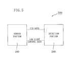
  • FIG. 5 is a block diagram showing a construction of the print state inspection apparatus.
  • a print state inspection apparatus 500 includes a sensor portion 100 that irradiates a print surface of a print W arranged at a predetermined position with light and picks up an image formed by reflected light from the print surface, and a detection portion 200 that analyzes image data obtained by the sensor portion and detects a print defect.
  • the sensor portion 100 is the sensor unit described above.
  • the print W in the case of a so-called off-line system, the print W extracted in accordance with inspection criteria is placed on a placement table and inspection is performed.
  • the print state inspection apparatus can be incorporated into a print apparatus and the print on a transport belt or a transport drum is inspected.
  • the detection portion 200 may have an arbitrary appropriate construction in the print state inspection apparatus.
  • image data captured by the image pickup portion of the sensor portion 100 is position-corrected instantaneously and an inspection for a defect (such as foreign matter, a stain, print fading) and color monitoring (such as ⁇ E, YMCK separation) are performed at the same time.
  • a defect such as foreign matter, a stain, print fading
  • color monitoring such as ⁇ E, YMCK separation
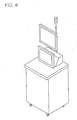
  • the print state inspection apparatus further includes an operation stand shown in FIG. 6.
  • the operation stand displays an image of an inspection target print on a screen in a real time manner, so visual inspection becomes extremely easy.
  • a technique of displaying image data from the sensor portion on the operation stand is not a feature of the present invention and is also widely known, so the detailed description thereof will be omitted here.
  • the sensor unit and the print state inspection apparatus according to the present invention are highly accurate and are also very compact, so attachment to a print apparatus that has conventionally been difficult becomes possible. Accordingly, the sensor unit according to the present invention is suitably applicable to a wide variety of print apparatuses.

Landscapes

  • Engineering & Computer Science (AREA)
  • Quality & Reliability (AREA)
  • Investigating Materials By The Use Of Optical Means Adapted For Particular Applications (AREA)

Abstract

A sensor unit 100 according to the present invention is a sensor unit 100 that irradiates a print surface with light and picks up an image formed by reflected light from the print surface and includes: an image pickup portion 10 including an image pickup element 11 and a lens 12 fitted to the image pickup element 11; an illumination portion 20 including a light-emission element 21 and a lens 22 fitted to the light-emission element 21; and a reflecting portion 30 including at least one mirror (31, 32) that reflects the reflected light from the print surface in a direction having a predetermined angle with respect to the direction of the normal to the print surface. According to the present invention, a sensor unit 100, which is highly accurate and whose miniaturization is possible, and a print state inspection apparatus using the sensor unit are provided.

Description

BACKGROUND OF THE INVENTION 1. Field of the Invention
The present invention relates to a sensor unit and a print state inspection apparatus using the sensor unit. More specifically, the present invention relates to a sensor unit, which is highly accurate and whose miniaturization is possible, and a print state inspection apparatus using the sensor unit.
2. Description of the Related Art
Conventionally, a print state inspection apparatus has been widely known which irradiates a print surface with light, picks up an image formed by reflected light from the print surface, and detects a print defect with reference to the obtained image.
FIG. 7 is a schematic construction diagram of an example of a conventional print state inspection apparatus. A print state inspection apparatus 700 shown in FIG. 7 is an inspection apparatus of so-called in-line type and continuously inspects print surfaces of prints transported. To do so, the apparatus 700 includes a sensor portion 710 and a print transport portion 720. The sensor portion 710 includes an image pickup element 71 and an illumination means 72. The illumination means 72 irradiates a print surface of a print W supplied to the transport portion with light, the image pickup element 71 captures an image formed by reflected light from the print surface, and a detection portion (not shown) detects a print defect by analyzing image data of the image.
The image pickup element 71 is preferably a CCD camera because it is possible to achieve high accuracy with the CCD camera. In the construction shown in FIG. 7, however, when it is attempted to pick up an image of the print surface in its entirety using the CCD camera, a distance between the CCD camera 71 and the print W becomes very long (ordinarily, a distance of 800 mm or more is required). Therefore, it is required to incorporate the sensor portion 710 into a print apparatus from an early stage of manufacture, which makes it impossible to commercialize the sensor portion alone. Also, when it is desired to improve the inspection accuracy of the print apparatus, it is required to modify or change an inspection apparatus incorporated into the print apparatus, which is very disadvantageous in terms of economy. Among inspection apparatuses using photosensors of low accuracy, there is an inspection apparatus whose sensor portion (sensor unit) is detachable (see JP 2002-333404 A, for instance). However, the miniaturization and detachable construction of a sensor unit of an inspection apparatus using a highly accurate CCD camera are not yet realized.
As described above, a sensor unit, which is highly accurate and whose miniaturization is possible, and a print state inspection apparatus using the sensor unit are strongly desired.
SUMMARY OF THE INVENTION
The present invention has been made in order to solve the above-mentioned problems with the prior art, and has an object to provide a sensor unit, which is highly accurate and whose miniaturization is possible, and a print state inspection apparatus using the sensor unit.
A sensor unit according to an embodiment of the present invention irradiates a print surface with light and picks up an image formed by reflected light from the print surface. The sensor unit comprises: an image pickup portion including an image pickup element and a lens fitted to the image pickup element; an illumination portion including a light-emission element and a lens fitted to the light-emission element; and a reflecting portion including at least one mirror that reflects the reflected light from the print surface in a direction having a predetermined angle with respect to a direction of normal to the print surface.
In one embodiment of the invention, the reflecting portion includes: a first mirror that reflects the reflected light from the print surface in a first direction having a predetermined angle with respect to the direction of the normal to the print surface; and a second mirror that reflects the light reflected in the first direction in a second direction having a predetermined angle with respect to the first direction.
In another embodiment of the invention, the first direction has an angle of 90 degrees with respect to the direction of the normal to the print surface, and the second direction has an angle of 90 degrees with respect to the first direction.
In still another embodiment of the invention, the image pickup element is a CCD camera, and the light-emission element is a high-intensity LED.
In still another embodiment of the invention, the first mirror and the second mirror are each an evaporated mirror.
According to another aspect of the present invention, a print state inspection apparatus is provided. The print state inspection apparatus irradiates a print surface of a print arranged at a predetermined position with light, picks up an image formed by reflected light from the print surface, and detects a print defect with reference to an obtained image. The print state inspection apparatus comprises: a sensor portion that irradiates the print surface with the light and picks up the image formed by the reflected light from the print surface; and a detection portion that detects the print defect by analyzing image data obtained by the sensor portion, wherein the sensor portion includes: an image pickup portion including an image pickup element and a lens fitted to the image pickup element; an illumination portion including a light-emission element and a lens fitted to the light-emission element; and a reflecting portion including at least one mirror that reflects the reflected light from the print surface in a direction having a predetermined angle with respect to a direction of normal to the print surface.
According to the present invention, a specific light-emission element is combined with an optical systemas an illumination portion, and a reflecting portion that uses a specific mirror is provided. As a result, it is possible to provide a sensor unit, which is highly accurate and whose miniaturization is possible, and a print state inspection apparatus using the sensor unit. As a matter of fact, according to the sensor unit of the present invention, it is possible to reduce the height of the unit to around 220 mm. In addition, it is possible to set a working distance (distance between a sensor lower end (in the vicinity of an illumination portion) and a print) at around 35 to 40 mm. Consequently, it is possible to set a distance between the CCD camera and the print at around only 250 mm, which is 1/4 or less of a distance in the case of the conventional CCD sensor.
BRIEF DESCRIPTION OF THE DRAWINGS
In the accompanying drawings:
  • FIG. 1 is a schematic construction diagram of a sensor unit according to a preferred embodiment of the present invention;
  • FIG. 2 is a schematic perspective view illustrating an entire external appearance of the sensor unit shown in FIG. 1;
  • FIG. 3 is a see-through schematic perspective view illustrating a state of an image pickup portion in the sensor unit;
  • FIG. 4 is a schematic construction diagram of a sensor unit according to another preferred embodiment of the present invention;
  • FIG. 5 is a block diagram showing a construction of a print state inspection apparatus according to a preferred embodiment of the present invention;
  • FIG. 6 is a schematic perspective view of an operation stand that is applicable to the print state inspection apparatus according to the present invention; and
  • FIG. 7 is a schematic construction diagram of an example of a conventional print state inspection apparatus.
  • DETAILED DESCRIPTION OF THE PREFERRED EMBODIMENTS
    Preferred embodiments of the present invention will now be described with reference to the accompanying drawings, although there is no intention to limit the present invention to the embodiments.
    FIG. 1 is a schematic construction diagram of a sensor unit according to a preferred embodiment of the present invention, FIG. 2 is a schematic perspective view illustrating an entire external appearance of the sensor unit shown in FIG. 1, and FIG. 3 is a see-through schematic perspective view illustrating a state of an image pickup portion in the sensor unit. A sensor unit 100 is a unit that irradiates a print surface of a print W with light and picks up an image formed by reflected light from the print surface. To do so, the sensor unit 100 includes an image pickup portion 10, an illumination portion 20, and a reflecting portion 30. The image pickup portion 10 includes an image pickup element 11 and a lens 12 fitted to the image pickup element 11. Also, the illumination portion 20 includes a light-emission element 21 and a lens 22 fitted to the light-emission element 21. Further, the reflecting portion 30 includes a first mirror 31 that reflects the reflected light from the print surface of the print W in a first direction D1 having a predetermined angle with respect to the direction of the normal to the print surface and a second mirror 32 that further reflects the light reflected in the first direction D1 in a second direction D2 having a predetermined angle with respect to the first direction. As shown in FIGS. 1 to 3, the image pickup portion 10 and the reflecting portion 30 are accommodated in a block-shaped housing 40 having an opening (portion through which the reflected light is introduced into the housing 40) 41 that extends in a lengthwise direction. The illumination portion 20 is fitted to an arbitrary appropriate portion of the housing 40 with an arbitrary appropriate means so as to illuminate the print surface of the print W in its entirety as appropriate.
    More specifically, the image pickup portion 10 is fitted in the housing 40 so that the image pickup element 11 and the lens 12 are directed in the same direction as the print surface (upward direction, in ordinary cases) . The image pickup element 11 is preferably a CCD camera. By using the CCD camera, detection of a color print at high resolution becomes possible. The lens 12 preferably has a wide angle and a short focal distance. A specifically preferable angle of view of the lens 12 is around 95 to 110 degrees and a specifically preferable focal distance thereof is around 12 to 20 mm. By using such a lens having a wide angle and a short focal distance, even with a very short working distance (distance between the sensor lower end and the print surface), it becomes possible to pick up an image in a predetermined region of the print surface in its entirety. As a result, it becomes possible to produce a highly miniaturized sensor unit and print state inspection apparatus.
    The illumination portion 20 is ordinarily provided in proximity to the opening 41 of the housing 40 in a direction parallel to the opening 41. The light-emission element 21 of the illumination portion 20 is preferably a high-intensity LED (typically, an ultra high-intensity white LED). The high-intensity LED has the following advantages: (1) its conversion efficiency from electricity to light is high, which enables energy saving; (2) it produces no heat, which is preferable also from the viewpoint of environment; (3) its lifespan is long (around 100,000 hours that is 15 or more times as long as the average lifespanof fluorescent tubes that is around 6, 000 hours), and even frequent turning on/off exerts no influence on the lifespan; (4) its lighting speed is extremely high; and (5) its size is small and its weight is light. The illuminance of the LED is preferably around 130 to 140 Lumens/W (which is around 1. 8 times as high as that of the fluorescent tube). In the illumination portion 20, many LEDs are arranged regularly. Typically, the LEDs are arranged in a multi-line manner. More preferably, the LEDs are arranged at a relatively low density in their center portions and are arranged at a relatively high density in their both end portions. As compared with a high-frequency fluorescent tube conventionally used as the illumination means, the LEDs suffer from less light amount shortage on both sides and have markedly stable light amounts in both end portions, so that their lateral length can be reduced. In addition, by using the LEDs arranged regularly and the specific lens 22 (to be described later) in combination, it becomes possible to uniformly irradiate the whole of a predetermined region of the print surface, so it becomes possible to send a clear image to the image pickup portion.
    The lens 22 of the illumination portion 20 has a shape with which it is possible to condense light irradiated from the light-emission element 21 on the print surface as appropriate. Typically, the lens 22 has an elliptic cylinder shape. By condensing light from the LEDs using such a lens, seam portions between adj acent LED elements can be made uniform, which makes it possible to irradiate the print with light having a line shape where no unevenness exists.
    The first mirror 31 and the second mirror 32 of the reflecting portion 30 are arranged so that the reflected light from the print surface of the print W enters the image pickup portion 10 (that is, the image pickup element 11 through the lens 12) as appropriate. Typically, the first mirror 31 is arranged so that the first direction D1 described above has an angle of 90 degrees with respect to the direction of the normal to the print surface and the second mirror 32 is arranged so that the second direction D2 described above has an angle of 90 degrees with respect to the first direction D1. As a result, the reflected light enters the image pickup portion 10 in a direction parallel to the direction of the normal to the print surface. More specifically, the first mirror 31 is arranged so as to define an angle of 45 degrees with respect to the direction of the normal to the print surface and the second mirror 32 is arranged so as to define an angle of 45 degrees with respect to the first direction D1. The first mirror 31 and the second mirror 32 are preferably each an evaporated mirror. The evaporated mirror is high in reflection efficiency and is small in light amount reduction after reflection as compared with an ordinary optical mirror, so it becomes possible to provide the image pickup portion 10 with a bright image. In addition, the reflection surface of the mirror is a highly smooth plane and has a structure with which it is possible to maintain as much as possible the light amount of the reflected light entering the image pickup portion.
    FIG. 4 is a schematic construction diagram of a sensor unit according to another preferred embodiment of the present invention. In this embodiment, a sensor unit 140 includes a first illumination portion 42 and a second illumination portion 43. The concrete constructions of the first and second illumination portions are the same as above. By providing the two illumination portions, it becomes possible to provide an image pickup portion 10 with a brighter and clearer image.
    In addition, a reflecting portion 30 includes only one mirror that reflects reflected light from a print surface of a print W in a direction having a predetermined angle (90 degrees, in this embodiment) with respect to the direction of the normal to the print surface. Therefore, the image pickup portion 10 is fitted in a housing 40 so that the light-reception direction of an image pickup element 11 and a lens 12 becomes a 90-degree direction with respect to the direction of the normal to the print surface. According to this embodiment, reflection is performed only once, so reflected light entering the image pickup portion suffers less reduction in light amount.
    With the sensor unit according to the present invention, it becomes possible to extremely reduce the size of the unit itself and it also becomes possible to extremely reduce the working distance (distance between the sensor lower end (in the vicinity of the illumination portion) and the print). As a matter of fact, the height of the block-shaped unit shown in FIGS. 1 to 3 is around 220 mm and the working distance thereof is around 35 to 40 mm. In the case of the conventional apparatus, the distance from the CCD camera to the print exceeds 1 m (1000 mm), so the present invention achieves miniaturization to 1/4 or less.
    Next, a print state inspection apparatus according to a preferred embodiment of the present invention will be described. FIG. 5 is a block diagram showing a construction of the print state inspection apparatus. A print state inspection apparatus 500 includes a sensor portion 100 that irradiates a print surface of a print W arranged at a predetermined position with light and picks up an image formed by reflected light from the print surface, and a detection portion 200 that analyzes image data obtained by the sensor portion and detects a print defect. The sensor portion 100 is the sensor unit described above. As to the arrangement of the print W, in the case of a so-called off-line system, the print W extracted in accordance with inspection criteria is placed on a placement table and inspection is performed. On the other hand, in the case of an in-line system, the print state inspection apparatus can be incorporated into a print apparatus and the print on a transport belt or a transport drum is inspected.
    The detection portion 200 may have an arbitrary appropriate construction in the print state inspection apparatus. In a typical operation at the detection portion 200, image data captured by the image pickup portion of the sensor portion 100 is position-corrected instantaneously and an inspection for a defect (such as foreign matter, a stain, print fading) and color monitoring (such as ΔE, YMCK separation) are performed at the same time.
    Preferably, the print state inspection apparatus according to the present invention further includes an operation stand shown in FIG. 6. The operation stand displays an image of an inspection target print on a screen in a real time manner, so visual inspection becomes extremely easy. A technique of displaying image data from the sensor portion on the operation stand is not a feature of the present invention and is also widely known, so the detailed description thereof will be omitted here.
    The sensor unit and the print state inspection apparatus according to the present invention are highly accurate and are also very compact, so attachment to a print apparatus that has conventionally been difficult becomes possible. Accordingly, the sensor unit according to the present invention is suitably applicable to a wide variety of print apparatuses.
    Many other modifications will be apparent to and be readily practiced by those skilled in the art without departing from the scope and spirit of the invention. It should therefore be understood that the scope of the appended claims is not intended to be limited by the details of the description but should rather be broadly construed.
    Claims (6)

    1. A sensor unit (100) that irradiates a print surface with light and picks up an image formed by reflected light from the print surface, the sensor unit (100) comprising:
      an image pickup portion (10) including an image pickup element (11) and a lens (12) fitted to the image pickup element (11);
      an illumination portion (20) including a light-emission element (21) and a lens (22) fitted to the light-emission element (21); and
      a reflecting portion (30) including at least one mirror (31, 32) that reflects the reflected light from the print surface in a direction having a predetermined angle with respect to a direction of normal to the print surface.
    2. A sensor unit (100) according to claim 1, wherein the reflecting portion (30) includes:
      a first mirror (31) that reflects the reflected light from the print surface in a first direction (D1) having a predetermined angle with respect to the direction of the normal to the print surface; and
      a second mirror (32) that reflects the light reflected in the first direction (D1) in a second direction (D2) having a predetermined angle with respect to the first direction (D1).
    3. A sensor unit (100) according to claim 2, wherein the first direction (D1) has an angle of 90 degrees with respect to the direction of the normal to the print surface, and wherein the second direction (D2) has an angle of 90 degrees with respect to the first direction (D1).
    4. A sensor unit (100) according to claim 1, wherein the image pickup element (11) is a CCD camera, and wherein the light-emission element (21) is a high-intensity LED.
    5. A sensor unit (100) according to claim 2, wherein the first mirror (31) and the second mirror (32) are each an evaporated mirror.
    6. A print state inspection apparatus (500) that irradiates a print surface of a print (W) arranged at a predetermined position with light, picks up an image formed by reflected light from the print surface, and detects a print defect with reference to an obtained image,
         the print state inspection apparatus (500) comprising:
      a sensor portion (100) that irradiates the print surface with the light and picks up the image formed by the reflected light from the print surface; and
      a detection portion (200) that detects the print defect by analyzing image data obtained by the sensor portion (100),
         wherein the sensor portion (100) includes:
      an image pickup portion (10) including an image pickup element (11) and a lens (12) fitted to the image pickup element (11);
      an illumination portion (20) including a light-emission element (21) and a lens (22) fitted to the light-emission element (21); and
      a reflecting portion (30) including at least one mirror (31, 32) that reflects the reflected light from the print surface in a direction having a predetermined angle with respect to a direction of normal to the print surface.
    EP05006590A 2004-03-29 2005-03-24 Sensor unit and print state inspection apparatus using the same Withdrawn EP1582350A1 (en)

    Applications Claiming Priority (2)

    Application Number Priority Date Filing Date Title
    JP2004094316A JP2005283199A (en) 2004-03-29 2004-03-29 Sensor unit and printing state inspection apparatus using the sensor unit
    JP2004094316 2004-03-29

    Publications (1)

    Publication Number Publication Date
    EP1582350A1 true EP1582350A1 (en) 2005-10-05

    Family

    ID=34879899

    Family Applications (1)

    Application Number Title Priority Date Filing Date
    EP05006590A Withdrawn EP1582350A1 (en) 2004-03-29 2005-03-24 Sensor unit and print state inspection apparatus using the same

    Country Status (4)

    Country Link
    US (1) US20050213795A1 (en)
    EP (1) EP1582350A1 (en)
    JP (1) JP2005283199A (en)
    CN (1) CN1677093A (en)

    Cited By (1)

    * Cited by examiner, † Cited by third party
    Publication number Priority date Publication date Assignee Title
    EP4043218A1 (en) 2021-02-11 2022-08-17 Heidelberger Druckmaschinen AG Printing machine with a device for conveying printed material and with a camera

    Families Citing this family (6)

    * Cited by examiner, † Cited by third party
    Publication number Priority date Publication date Assignee Title
    DE102005061834B4 (en) * 2005-12-23 2007-11-08 Ioss Intelligente Optische Sensoren & Systeme Gmbh Apparatus and method for optically examining a surface
    DE102006006136A1 (en) * 2006-02-10 2007-08-23 Koenig & Bauer Aktiengesellschaft Systems for checking the assembly of a printing forme magazine and a system for feeding at least one printing form stored in a printing forme magazine to a cylinder
    JP5012006B2 (en) * 2006-12-27 2012-08-29 ダックエンジニアリング株式会社 Inspection unit
    DE102007002106B3 (en) * 2007-01-09 2008-07-03 Wolfgang Weinhold Object's surface configuration examining device, has control and evaluation unit connected with light sources and light sensor, where light sources are arranged such that optical radiation axis runs in different reference planes
    EP2905136B1 (en) * 2014-02-07 2018-03-28 Müller Martini Holding AG Method and apparatus for monitoring a print processing machine
    US10515246B2 (en) 2017-03-10 2019-12-24 Cognex Corporation Code reader with extended reading range

    Citations (2)

    * Cited by examiner, † Cited by third party
    Publication number Priority date Publication date Assignee Title
    JPH0196537A (en) * 1987-10-08 1989-04-14 Hitachi Electron Eng Co Ltd Glass disk flaw identification method and flaw detecting optical device
    US5664025A (en) * 1992-10-16 1997-09-02 Insinooritoimisto Data Oy Apparatus for the quality control of a print produced by a printing machine

    Family Cites Families (1)

    * Cited by examiner, † Cited by third party
    Publication number Priority date Publication date Assignee Title
    US6498867B1 (en) * 1999-10-08 2002-12-24 Applied Science Fiction Inc. Method and apparatus for differential illumination image-capturing and defect handling

    Patent Citations (2)

    * Cited by examiner, † Cited by third party
    Publication number Priority date Publication date Assignee Title
    JPH0196537A (en) * 1987-10-08 1989-04-14 Hitachi Electron Eng Co Ltd Glass disk flaw identification method and flaw detecting optical device
    US5664025A (en) * 1992-10-16 1997-09-02 Insinooritoimisto Data Oy Apparatus for the quality control of a print produced by a printing machine

    Non-Patent Citations (1)

    * Cited by examiner, † Cited by third party
    Title
    PATENT ABSTRACTS OF JAPAN vol. 013, no. 332 (P - 905) 26 July 1989 (1989-07-26) *

    Cited By (3)

    * Cited by examiner, † Cited by third party
    Publication number Priority date Publication date Assignee Title
    EP4043218A1 (en) 2021-02-11 2022-08-17 Heidelberger Druckmaschinen AG Printing machine with a device for conveying printed material and with a camera
    EP4043217A1 (en) 2021-02-11 2022-08-17 Heidelberger Druckmaschinen AG Printing machine with a device for conveying printed material and with a camera
    CN114919284A (en) * 2021-02-11 2022-08-19 海德堡印刷机械股份公司 Printing machine with a device for feeding printing material and with a camera

    Also Published As

    Publication number Publication date
    CN1677093A (en) 2005-10-05
    JP2005283199A (en) 2005-10-13
    US20050213795A1 (en) 2005-09-29

    Similar Documents

    Publication Publication Date Title
    CN101726499B (en) Surface inspection apparatus
    JP3249509B2 (en) Automatic high-speed optical inspection equipment
    US8363214B2 (en) Surface inspection apparatus
    JP4511978B2 (en) Surface flaw inspection device
    US20050213795A1 (en) Sensor unit and print state inspection apparatus using the same
    US20090202148A1 (en) Image Capturing System and Method for the Analysis of Image Data
    JP2008292273A (en) Pattern inspection apparatus and pattern inspection method
    JP2011089939A (en) Appearance inspection apparatus and printed solder inspection apparatus
    TWI458965B (en) Image capturing system and method for analysis of image data
    US7965917B2 (en) Illuminating apparatus and surface inspection system using illuminating apparatus
    JP3585214B2 (en) Strip sheet inspection device
    KR20060053847A (en) Defect inspection method of glass plate and device
    JP2005188929A (en) Work inspection device
    JP2003514121A5 (en)
    JP2011106912A (en) Imaging illumination means and pattern inspection device
    JP2019120540A (en) Defect inspection device, and defect inspection device manufacturing method
    US20130222569A1 (en) Imaging apparatus
    JP5948974B2 (en) Surface defect inspection equipment
    JP3575678B2 (en) Defect detection method and apparatus for plate-shaped transparent body
    JP2008128811A (en) Defect inspection device
    JP2000123152A (en) Image input device
    JP2007033295A (en) Inspection device
    JP7560149B2 (en) Illumination device and imaging system
    JPH11241917A (en) Plate shape detection method and device
    KR100855539B1 (en) High Illumination LED Lighting

    Legal Events

    Date Code Title Description
    PUAI Public reference made under article 153(3) epc to a published international application that has entered the european phase

    Free format text: ORIGINAL CODE: 0009012

    AK Designated contracting states

    Kind code of ref document: A1

    Designated state(s): AT BE BG CH CY CZ DE DK EE ES FI FR GB GR HU IE IS IT LI LT LU MC NL PL PT RO SE SI SK TR

    AX Request for extension of the european patent

    Extension state: AL BA HR LV MK YU

    17P Request for examination filed

    Effective date: 20060314

    AKX Designation fees paid

    Designated state(s): AT BE BG CH CY CZ DE DK EE ES FI FR GB GR HU IE IS IT LI LT LU MC NL PL PT RO SE SI SK TR

    STAA Information on the status of an ep patent application or granted ep patent

    Free format text: STATUS: THE APPLICATION HAS BEEN WITHDRAWN

    18W Application withdrawn

    Effective date: 20080328