BACKGROUND OF THE INVENTION
-
The present invention relates to a lighting apparatus.
Specifically, the present invention relates to a lighting
apparatus having a plurality of luminescent panels, in which
each panel includes a light emitting portion for emitting
isotropic light such as an electroluminescent element (EL
element), and a non-light emitting portion provided around
the light emitting portion (EL element), and the panels are
arranged so that the non-light emitting portions are
adjacent to each other.
-
The present invention also relates to a lighting
apparatus having a luminescent panel that includes a light
emitting portion for emitting isotropic light such as an EL
element, and a non-light emitting portion.
-
Conventionally, lighting apparatuses having EL elements
arranged on a transparent substrate have been proposed.
There has also been proposed a technique for using such
lighting apparatus as a backlight for a liquid crystal
display. There is a demand for large-area EL elements.
However, EL elements are extremely thin, having an EL layer
of thickness of several tens to several hundreds nanometers.
It is thus difficult to uniformly form an EL layer in a
large area. Such attempt would result in a reduced yield.
-
Also, there is proposed an EL display that is formed by
joining display panels. This EL display does not degrade a
light emitting portion and makes junctions of the display
panels inconspicuous (for example, refer to Japanese Laid-Open
Patent Publication No. 2002-297065). In this EL
display, light emitting layers 60a, 60b are separated by
protective layers 61a, 61b as shown in Fig. 16. Edges of
compact panels 62a, 62b are beveled at the upper and lower
surfaces. Adhesive 63 fills a narrow space between facing
pair of the protective layers 61a, 61b of compact panels
62a, 62b. The adhesive 63 also fills upper and lower spaces
located above and below the narrow space. Accordingly, the
compact panels 62a, 62b are joined to each other.
Specifically, the compact panels 62a, 62b are joined to each
other so that the pixel pitch at the junction between the
compact panels 62a, 62b (the distance between an adjacent
pair of the light emitting layers 60a, 60b) is equal to the
pixel pitch in each of the compact panels 62a, 62b (the
distance between each adjacent pair of the light emitting
layers 60a and the distance between each adjacent pair of
the light emitting layers 60b). The compact panels 62a, 62b
are attached to a protective substrate 64 with the adhesive
63. To reduce optical imperfections, an adhesive having
optical properties that is close to the refractive index of
glass in the visible wavelength range is used as the
adhesive 63. For example, an ultraviolet curing adhesive or
a polymeric adhesive is used as the adhesive 63.
-
In a typical organic EL element, some of light emitted
from fluophor in a light emitting layer is totally reflected
at an interface between air and a transparent substrate at a
light extracting side. The totally reflected light cannot
be effectively used. There have been proposed a number of
organic EL elements that are designed to reduce such a
disadvantage (for example, refer to Japanese Laid-Open
Patent Publication No. 2003-397052). In the organic EL
element of the publication, an anode 66, a hole transport
layer 67, a light emitting layer 68, and a transparent
cathode 69 are laminated on a substrate 65 as shown in Fig.
17. An unillustrated protective film is formed on the
cathode 69. A light angle changing panel 70 is attached to
the protective film with an optical adhesive. V-shaped
grooves 71 are formed on a surface of the angle changing
panel 70 that faces the substrate 65. Without the V-shaped
grooves 71, some of light emitted by the light emitting
layer 68 is totally reflected on a light emitting surface
(light exit surface) 70a and is trapped in the EL element.
However, since the EL element of Fig. 17 has the V-shaped
grooves 71, light that is inclined with respect to the light
emitting surface (light exit surface) 70a is totally
reflected at interface between each V-shaped groove 71 and
air so that the angle of the light is changed. The light
then exits to the air. This improves the light extraction
efficiency.
-
Further, there have been proposed organic EL panels
that improve the utilization of light to obtain a bright
image (for example, refer to Japanese Laid-Open Patent
Publication No. 2003-282255). The organic EL panel of the
publication has organic EL elements, which function as
pixels. The organic EL elements are formed in a matrix and
as a film on a first transparent substrate. A second
transparent substrate is located on the organic EL film.
The second transparent substrate is fixed to the organic EL
film with an adhesive layer. On a surface of the second
transparent substrate that faces the first transparent
substrate, V-shaped grooves of a grid pattern are formed
except for sections corresponding to the pixels. A
reflection film is formed on each inclined surface of the V-shaped
grooves. Light that is incident from each organic EL
element and on the second transparent substrate, and
advances toward a side of the second transparent substrate
is reflected by one of the reflection films and exits the
second transparent substrate.
-
The EL display disclosed in Japanese Laid-Open Patent
Publication No. 2002-297065 has no pixels at the junction
between the compact panels 62a, 62b. The junctions are
therefore non-light emitting portions. Therefore, it is not
necessary that light having a brightness equal to the
brightness of sections corresponding to the light emitting
layers 60a, 60b be emitted from sections corresponding to
the adhesive 63. Therefore, the art of this publication has
no optical problems as a method for joining the compact
panels 62a, 62b to each other. However, when applied to a
panel in a lighting apparatus used as a backlight for a
liquid crystal display, the method has the following
drawbacks. For example, light emitted from the light
emitting layers 60a, 60b toward the edges of the compact
panels 62a, 62b is reflected, absorbed, or dispersed at
interfaces between the adhesive 63 and the beveled edges of
the compact panels 62a, 62b. Also, light that passes
through the adhesive 63 is absorbed or dispersed by the
adhesive 63. As a result, the brightness of the section of
the adhesive 63 is less than the brightness of other
sections. As a result, the boundary between the compact
panels 62a, 62b becomes dim. Also, if cracks are caused
while beveling the edges of the compact panels 62a, 62b, the
cracks would affects the apparatus, and the compact panels
62a, 62b with cracks therefore cannot be used. This reduces
yields.
-
Japanese Laid-Open Patent Publications No. 2003-347052
and No. 2003-282255 do not disclose or suggest any technique
for enlarging the size of screens of organic EL elements.
The objectives of the publications are to extract light that
is emitted by light emitting layers but conventionally
cannot be extracted due to total reflection, for example, at
light exit surfaces. However, the publications do not
disclose or suggest any technique for obtaining a lighting
apparatus with a large light emitting area by causing the
same brightness of light to be emitted from sections
corresponding to non-light emitting portions of organic EL
elements as the brightness of light emitting sections of the
EL elements.
SUMMARY OF THE INVENTION
-
Accordingly, it is an objective of the present
invention to provide a lighting apparatus having a plurality
of luminescent panels emitting isotropic light, which
apparatus eliminates necessity for cutting the luminescent
panels and effectively uses light from light emitting
portions, thereby preventing sections facing non-light
emitting portions between luminescent panels from becoming
dim.
-
Another objective of the present invention is to
provide a lighting apparatus having a luminescent panel with
a light emitting portion and a non-light emitting portion,
the light emitting portion emitting isotropic light, which
apparatus emits light from a light exit portion, the area of
which is larger than that of the light emitting portion, and
in which apparatus the brightness of a section of the light
exit portion that corresponds to the light emitting portion
is substantially equal to the brightness of a section of the
light exit portion that corresponds to the non-light
emitting portion.
-
To achieve the above-mentioned objective, the present
invention provides a lighting apparatus. A luminescent
panel has a light emitting portion for emitting isotropic
light and a non-light emitting portion. A brightness
compensating member has an incident portion, on which light
is incident, and a light exit portion, through which light
exits. The incident portion includes at least one inclined
surface that is inclined relative to the light exit portion.
The inclined surface is arranged to correspond to the non-light
emitting portion. The inclined surface is configured
so that the brightness of a section of the brightness
compensating member that corresponds to the light emitting
portion is substantially equal to the brightness of a
section of the brightness compensating member that
corresponds to the non-light emitting portion.
-
Further, the present invention provides a lighting
apparatus including a plurality of luminescent panels. Each
luminescent panel has a light emitting portion for emitting
isotropic light and a non-light emitting portion provided
around the light emitting portion. The luminescent panels
are arranged so that the non-light emitting portions are
adjacent to each other. A brightness compensating member is
formed of a transparent plate and is arranged at a side of
the luminescent panels through which light exits to
correspond to the luminescent panels. A surface of the
brightness compensating member that faces the luminescent
panels has a V-shaped groove that extends along the non-light
emitting portions. The V-shaped groove is formed so
that the brightness of a section of the brightness
compensating member that corresponds to the light emitting
portion is substantially equal to the brightness of a
section of the brightness compensating member that
corresponds to the non-light emitting portions.
-
Further, the present invention provides a lighting
apparatus including a plurality of adjoining luminescent
panels each having a light emitting portion for emitting
isotropic light and an auxiliary electrode. A section of
each luminescent panel on which the auxiliary electrode is
formed forms a non-light emitting portion. A brightness
compensating member is formed of a transparent plate and is
arranged at a side of the luminescent panels through which
light exits to correspond to the luminescent panels. A
surface of the brightness compensating member that faces the
luminescent panels has a V-shaped groove that is arranged to
correspond to the non-light emitting portions. The V-shaped
groove is formed so that the brightness of a section of the
brightness compensating member that corresponds to the light
emitting portions is substantially equal to the brightness
of a section of the brightness compensating member that
corresponds to the non-light emitting portions.
-
Further, the present invention provides a lighting
apparatus including a plurality of luminescent panels each
having a light emitting portion for emitting isotropic light
and a non-light emitting portion provided around the light
emitting portion. The luminescent panels are arranged so
that the non-light emitting portions are adjacent to each
other. A brightness compensating member is formed of a
transparent plate and is arranged at a side of the
luminescent panels through which light exits to correspond
to the luminescent panels. A surface of the brightness
compensating member that faces the luminescent panels has a
V-shaped groove that extends along the non-light emitting
portions. The V-shaped groove is formed so that the
brightness of a section of the brightness compensating
member that corresponds to the non-light emitting portion is
increased to approaches the brightness of a section of the
brightness compensating member that corresponds to the light
emitting portions.
-
Other aspects and advantages of the invention will
become apparent from the following description, taken in
conjunction with the accompanying drawings, illustrating by
way of example the principles of the invention.
BRIEF DESCRIPTION OF THE DRAWINGS
-
The invention, together with objects and advantages
thereof, may best be understood by reference to the
following description of the presently preferred embodiments
together with the accompanying drawings in which:
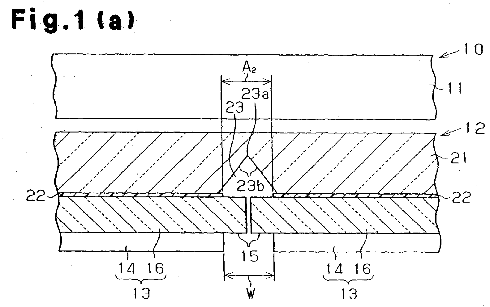
- Fig. 1(a) is a partial cross-sectional view
illustrating a liquid crystal display provided with a
lighting apparatus according to a first embodiment of the
present invention;
- Fig. 1(b) is a partial cross-sectional view of the
luminescent panel shown in Fig. 1(a);
- Fig. 2 is a diagrammatic view showing an operation of
the lighting apparatus shown in Fig. 1(a);
- Fig. 3 is a partial plan view illustrating the lighting
apparatus shown in Fig. 1(a);
- Figs. 4(a) and 4(b) are diagrammatic views for
obtaining relational equations between the viewing angle and
the apex angle of a V-shaped groove in the lighting
apparatus shown in Fig. 1(a);
- Fig. 5 is a partial cross-sectional view illustrating a
liquid crystal display provided with a lighting apparatus
according to a second embodiment of the present invention;
- Fig. 6 is a partial cross-sectional view illustrating a
liquid crystal display provided with a lighting apparatus
according to a third embodiment of the present invention;
- Fig. 7 is a partial cross-sectional view illustrating a
liquid crystal display provided with another lighting
apparatus according to the third embodiment of the present
invention;
- Figs. 8(a), 8(b), and 8(c) are diagrammatic views
showing the relationship of the viewing angle, the apex
angle of a V-shaped groove, the apex angle of a second V-shaped
groove, and the thickness of a brightness
compensating member;
- Fig. 9 is a plan view illustrating a lighting apparatus
according to a fourth embodiment of the present invention;
- Fig. 10 is a partial cross-sectional view illustrating
the lighting apparatus shown in Fig. 9;
- Fig. 11 is a diagrammatic view showing the relationship
of the viewing angle, the inclined surface, and the
thickness of the brightness compensating member of the
lighting apparatus shown in Fig. 9;
- Fig. 12 is a plan view illustrating a luminescent panel
according to a fifth embodiment of the present invention;
- Fig. 13 is a partial cross-sectional view illustrating
the lighting apparatus shown in Fig. 12;
- Fig. 14 is a partial cross-sectional view illustrating
a lighting apparatus according to another embodiment of the
present invention;
- Fig. 15(a) is a partial cross-sectional view
illustrating a lighting apparatus according to a further
embodiment of the present invention;
- Fig. 15(b) is a partial cross-sectional view of the
luminescent panel shown in Fig. 15(a);
- Fig. 16 is a partial cross-sectional view illustrating
a prior art EL display; and
- Fig. 17 is a partial cross-sectional view illustrating
another prior art EL display.
-
DETAILED DESCRIPTION OF THE PREFERRED EMBODIMENTS
-
A lighting apparatus 12 according to a first embodiment
of the present invention will now be described referring to
Figs 1(a) to 4(b). The lighting apparatus 12 is used as a
backlight of a liquid crystal display 10. In the cross-sectional
views, part of hatching is omitted.
-
As shown in Fig. 1(a), the liquid crystal display 10
includes a transmissive liquid crystal panel 11 and the
lighting apparatus 12 located on the back of the liquid
crystal panel 11, or on a surface at a side opposite to a
display surface. The lighting apparatus 12 has luminescent
panels 13. Each luminescent panel 13 includes a light
emitting portion 14, which emits isotropic light, and a non-light
emitting portion 15 provided around the light emitting
portion 14. The luminescent panels 13 are arranged so that
the non-light emitting portions 15 are arranged adjacent to
each other. The number of the luminescent panels 13 is
determined according the size of each luminescent panel 13
and the size of the lighting apparatus 12. The luminescent
panels 13 are aligned in one or more rows. In this
embodiment, the luminescent panels 13 are aligned in a
plurality of rows as shown in Fig. 3. In this
specification, "to emit isotropic light" refers to a state
where light emitted by each light emitting portion 14 is
directed in every direction with an equal intensity.
-
As shown in Fig. 1(b), each luminescent panel 13
includes a transparent substrate 16 and an
electroluminescent element (EL element), which functions as
the light emitting portion 14, provided on the substrate 16.
In this embodiment, glass substrates are used as the
transparent substrates 16, and organic EL elements are used
as the EL elements. Each organic EL element includes a
first electrode 17, an organic EL layer 18, and a second
electrode 19, which are laminated in this order on the
transparent substrate 16. Each organic EL element is coated
with a protective film 20, so that the organic EL layer 18
is not adversely affected by water (water vapor) and oxygen.
In this embodiment, each first electrode 17 forms an anode,
and each second electrode 19 forms a cathode. Each organic
EL element is a "bottom emission type", in which light from
the organic EL layer 18 is extracted through the transparent
substrate 16. Therefore, the first electrodes 17 are of a
light transmission type, and the second electrodes 19 are of
a light reflection type. The first electrodes 17, the
organic EL layers 18, the second electrodes 19, and the
protective films 20 each have the materials and
configurations used in known organic EL elements. The
organic EL elements may be ones that have an emission
spectrum only in part of the visible range may be used.
-
The EL element, or the light emitting portion 14,
formed on each transparent substrate 16 needs to have
terminal electrodes and connecting lines (neither is shown)
for connecting the anode and cathode with, for example, an
external drive circuit. The terminal electrodes and
connecting lines are provided around the EL element on each
transparent substrate 16, on which the EL element is formed.
Since no light exits from this section even if the EL
element emits light, the section is referred to as the non-light
emitting portion 15.
-
As shown in Fig. 1(a), the transparent substrates 16 of
the luminescent panels 13 are attached to a brightness
compensating member 21, which is formed of a transparent
plate, with an adhesive 22. That is, the brightness
compensating member 21 is located at a side of the
luminescent panels 13 through which light exits and at a
position corresponding to the luminescent panels 13.
"Transparent" refers to a property of having transparency to
light of wavelength emitted by the light emitting portions
14, and generally, to a property of having a transmittance
of 70% or more to visible light. The adhesive 22 is an
ultraviolet curing adhesive or a polymeric adhesive having
the same or similar refractive index as the brightness
compensating member 21. To have a "similar refractive
index" refers to a state where the difference in the
refractive index between the adhesive 22 and the brightness
compensating member 21 is no more than several percent.
-
The brightness compensating member 21 may be made of
any material that is transparent and easy to machine. For
example, an acrylic resin, glass, polyvinyl chloride,
polyethylene, polystyrene, or polycarbonate may be used. In
this embodiment, the brightness compensating member 21 is
formed of the same glass as that of the transparent
substrate 16.
-
The brightness compensating member 21 may be made by
using a mold or by machining the surface of a plate-like
substrate.
-
V-shaped grooves 23 are formed on a surface of the
brightness compensating member 21 that faces the luminescent
panels 13. Each V-shaped groove 23 is located in a position
that corresponds to the non-light emitting portions 15 and a
section between the non-light emitting portions 15 of an
adjacent pair of the luminescent panels 13. The V-shaped
grooves 23 are configured so that the brightness of sections
of the brightness compensating member 21 that correspond to
the light emitting portions 14 is substantially the equal to
the brightness of sections of the brightness compensating
member 21 that correspond to the non-light emitting portions
15. In other words, the V-shaped grooves 23 are configured
so that the brightness of sections of the brightness
compensating member 21 that correspond to the non-light
emitting portions 15 is increased to approach the brightness
of sections of the brightness compensating member 21 that
correspond to the light emitting portions 15. A state where
"the brightness of sections of the brightness compensating
member 21 that correspond to the light emitting portions 14
is substantially equal to the brightness of sections of the
brightness compensating member 21 that correspond to the
non-light emitting portions 15" refers to a state where the
ratio of the luminance of the sections of the brightness
compensating member 21 that correspond to the light emitting
portions 14 to the luminance of the sections of the
brightness compensating member 21 that correspond to the
non-light emitting portions 15 is no less than 0.8 in the
present embodiment, in which the lighting apparatus 12 is
used as the backlight of the liquid crystal display 10. In
a case where the lighting apparatus 12 used as an ordinary
lighting apparatus, the state of substantially equal
brightness refers to a state where the luminance ratio is no
less than 0.5.
-
Inclined surfaces 23b of each V-shaped groove 23 are
either optically polished or mirror finished. The width A2
of the open end of each V-shaped groove 23 is wider than the
width W of the space between the light emitting portions 14
of the corresponding pair of the luminescent panels 13.
That is, the luminescent panels 13 are adhered to the
brightness compensating member 21 so that the end of each
light emitting portion 14 is located in the corresponding V-shaped
groove 23 when the brightness compensating member 21
is viewed from the side of the luminescent panels 13. The
degree by which the width A2 of the open end of each V-shaped
groove 23 is wider than the width W between the light
emitting portions 14 of the corresponding two luminescent
panels 13 is set so that the width A2 of the open end is not
made narrower than the width W due to an error within
tolerance when the brightness compensating member 21 is
machined.
-
Each V-shaped groove 23 is formed so that the depth A1
of the V-shaped groove 23, the width A2 of the open end of
the V-shaped groove 23, the apex angle α of the V-shaped
groove 23, the refractive index N1 of air, the refractive
index N2 of the brightness compensating member 21, and the
viewing angle of the brightness compensating member 21
satisfy the following two equations.
A1 = A2/{2tan(α/2)}
e = arcsin[(N2/N1)sin{90 - α/2 - arcsin(N1/N2)}]
-
The "viewing angle" refers to an angle defined by the
direction closest to the luminescent panels 13 among
directions in which the non-light emitting portions 15 of
each adjacent luminescent panel 13 are not visible when the
lighting apparatus 12 is viewed from the side of the
brightness compensating member 21, and the normal vector to
a plane of the brightness compensating member 21 except for
the V-shaped grooves 23, which normal vector is
perpendicular to the luminescent panels 13. The width A2 of
the open end of each V-shaped groove 23 is determined in
accordance with the width of each non-light emitting portion
15 of the luminescent panels 13. The refractive index N1 of
air cannot be changed. Also, the refractive index N2 of the
brightness compensating member 21 cannot be changed by a
great degree. Thus, the apex angle α of the V-shaped
grooves 23 and the depth A1 of the V-shaped grooves 23 are
determined appropriately depending on which of reduction of
the thickness of the brightness compensating member 21 and
increase of the viewing angle e is given a higher priority.
-
An operation of the lighting apparatus 12 configured as
described above will hereafter be described.
-
When voltage is applied to the first electrodes 17 and
the second electrodes 19 through a drive control apparatus
(not shown), the light emitting portions 14 of each
luminescent panel 13 emit light. Light emitted by the light
emitting portions 14 is incident on the brightness
compensating member 21 through the transparent substrates 16
and the adhesive 22. Due to the isotropic property of the
light emitting portions 14, part of light emitted by each
light emitting portion 14 advances in a slanting direction
toward the edge of the corresponding luminescent panel 13
through the transparent substrate 16. Then, as shown in
Fig. 2, part of light that is incident on the brightness
compensating member 21 in a slanting direction is reflected
at the inclined surfaces 23b of each V-shaped groove 23 and
advances in a direction perpendicular to the light exit
surface of the brightness compensating member 21.
-
Therefore, the same brightness is obtained from
sections of the lighting apparatus 12 each of which
corresponds to the non-light emitting portions 15 of an
adjacent pair of the luminescent panels 13 as the brightness
from sections of the lighting apparatus 12 that correspond
to the light emitting portions 14. Therefore, sections of
the lighting apparatus 12 corresponding to the non-light
emitting portions 15 between the luminescent panels 13 are
prevented from becoming dim. Light that exits through the
light exit surface of the brightness compensating member 21
toward the liquid crystal panel 11 is effectively used as
illuminating light of the lighting apparatus 12. A user of
the liquid crystal display 10 can see the things displayed
on the liquid crystal panel 11 with the illuminating light
of the lighting apparatus 12.
-
Referring to Figs. 4(a) and 4(b), the procedure for
obtaining the equations (1), (2), which define the
relationship between the viewing angle and the apex angle
α of the brightness compensating member 21, will now be
explained. The viewing angle is defined by a straight
line perpendicular to the light exit surface of the
brightness compensating member 21 and the direction of light
that exits the brightness compensating member 21 after
reaching one of the inclined surface 23b of one of the V-shaped
groove 23 at an incident angle of 90 degrees from the
outside of the brightness compensating member 21. The
following equation is satisfied when depth of each V-shaped
groove 23 is expressed by A1, the width of the open end of
each V-shaped groove 23 is expressed by A2, and the apex
angle of each V-shaped groove 23 is expressed by α as shown
in Fig. 4(a).
tan(α/2) - (A2/2)/A1
-
As shown in Fig. 4(b), with respect to light that is
incident on each inclined surface 23b of each V-shaped
groove 23 from the outside at an incident angle of 90
degrees, the following equation is satisfied due to Snell's
law if the incident angle 1 to the inclined surface 23b of
the V-shaped groove 23 is 90 degrees, the refractive angle
is expressed by 2, and the incident angle of the light
exiting from the brightness compensating member 21 to an air
layer is expressed by γ1.
N1sin = N2sin(γ1)
N2sin(2) = N1sin(1) = N1
2 + γ1 + α/2 = 90
-
Therefore, the equation (1) defining the depth A1 of
each V-shaped groove 23 is obtained based on the equation
(3), and the equation (2) defining the viewing angle is
obtained based on the equations (4) to (6).
A1 = (A2/2)/{tan(α/2) } = A2/{2tan(α/2)}
= arcsin [(N2/N1) sin{ 90 - α/2 - arcsin (N1/N2)}]
-
For example, if the apex angle α is set to 12.5 degrees
when the width A2 of the open end of each V-shaped groove 23
is 2.2 mm, the viewing angle is approximately 82 degrees,
and the depth A1 of each V-shaped groove 23 is 10.0 mm.
Further, if the apex angle α is set to 40 degrees when the
width A2 of the open end of each V-shaped groove 23 is 2.2
mm, the viewing angle is approximately 44 degrees, and the
depth A1 of each V-shaped groove 23 is 3.0 mm. Thus, by
forming the brightness compensating member 21 so that the
equations (1) and (2) are satisfied, the apex angle α of the
V-shaped grooves 23 and the depth A1 of the V-shaped grooves
23 are easily determined appropriately depending on which of
reduction of the thickness of the brightness compensating
member 21 and increase of the viewing angle is given a
higher priority.
-
This embodiment provides the following advantages.
- (1) The luminescent panels 13 are aligned and joined to
each other. Thus, compared to a case where a single
luminescent panel is used, a larger area can be illuminated.
- (2) The lighting apparatus 12 includes the luminescent
panels 13 each having the light emitting portion 14, which
emits isotropic light, and the non-light emitting portion 15
provided around the light emitting portion 14. The
luminescent panels 13 are arranged so that the non-light
emitting portions 15 are adjacent to each other. The
brightness compensating member 21 is located at a side of
the luminescent panels 13 through which light exits and at a
position corresponding to the luminescent panels 13. The V-shaped
grooves 23 are formed on a surface of the brightness
compensating member 21 that faces the luminescent panels 13.
Each V-shaped groove 23 is located in a position that
corresponds to the non-light emitting portions 15 and a
section between the non-light emitting portions 15 of an
adjacent pair of the luminescent panels 13. The V-shaped
grooves 23 are configured so that the brightness of sections
of the brightness compensating member 21 that correspond to
the light emitting portions 14 is substantially equal to the
brightness of sections of the brightness compensating member
21 that correspond to the non-light emitting portions 15.
Therefore, the luminescent panels 13 do not need to be
machined, and light from the light emitting portions 14 is
effectively used, thereby preventing sections of the
lighting apparatus 12 that correspond to the non-light
emitting portions 15 between the luminescent panes 13 from
becoming dim.
- (3) The width A2 of the open end of each V-shaped
groove 23 is wider than the width W of the space between the
light emitting portions 14 of the corresponding pair of the
luminescent panels 13. Therefore, even if the width A2 of
the open end of each V-shaped groove 23 is not precisely
equal to the width W of the space between the light emitting
portions 14 of the corresponding luminescent panels 13,
machining the V-shaped grooves 23 within a tolerable error
prevents the non-light emitting portions 15 from being
visible. In other words, linear dim sections do not appear
on the lighting apparatus 12.
- (4) The inclined surfaces 23b of each V-shaped groove
23 are either optically polished or mirror finished.
Therefore compared to a case where the inclined surfaces 23b
of each V-shaped groove 23 are not optically polished or
mirror finished, attenuation of light due to scattering and
absorption is reduced. Thus, the amount of light that is
reflected by the V-shaped grooves 23 and exits through the
light exit side of the brightness compensating member 21 is
increased. That is, light emitted by the light emitting
portions 14 is effectively used.
- (5) Each V-shaped groove 23 is formed so that the depth
A1 of the V-shaped groove 23, the width A2 of the open end of
the V-shaped groove 23, the apex angle α of the V-shaped
groove 23, the refractive index N1 of air, the refractive
index N2 of the brightness compensating member 21, and the
view angle satisfy the following two equations.
A1 = A2/{2tan(α/2)}
= arcsin[(N2/N1)sin{90 - α/2 - arcsin(N1/N2)}]
Thus, the apex angle α of the V-shaped grooves 23 and
the depth A1 of the V-shaped grooves 23 are easily determined
appropriately depending on which of reduction of the
thickness of the brightness compensating member 21 and
increase of the viewing angle is given a higher priority.
- (6) The luminescent panels 13 are attached to the
brightness compensating member 21 with the adhesive 22.
Therefore, compared to a configuration in which liquid or
gel, the refractive index of which is close to those of the
transparent substrates 16 and the brightness compensating
member 21, is located between the luminescent panels 13 and
the brightness compensating member 21, the assembly of the
luminescent panels 13 and the brightness compensating member
21 is facilitated.
- (7) The light emitting portions 14 are formed of EL
elements. Therefore, the light emitting portions 14, which
emit isotropic light, are easily formed or easy to come by.
- (8) The light emitting portions 14 are formed of
organic EL elements. Thus, compared to a case where
inorganic EL elements are used, the light emitting portions
14 are driven by a lower voltage.
- (9) The lighting apparatus 12 is used as the backlight
of the liquid crystal display 10. Brightness unevenness in
the liquid crystal,display 10 of a large screen is thus
reduced.
A second embodiment of the present invention will now
be described with reference to Fig. 5. A lighting apparatus
12 of the present embodiment is different from the lighting
apparatus 12 of the first embodiment in that the apparatus
12 of the present embodiment is suitable for use in a color
liquid crystal display. Specifically, the lighting
apparatus 12 of the second embodiment is different form the
first embodiment in that light emitting portions 14 emit
white light, and that light of the same color exits from the
entire light exit surface of a brightness compensating
member 21. Similar or the same reference numerals are given
to those components that are similar or the same as the
corresponding components of the first embodiment and
detailed explanations are omitted. Fig. 5 is partial cross-sectional
view illustrating a liquid crystal display 10.Organic EL layers 18 (see Fig. 1(b)) of organic EL
elements forming the light emitting portions 14 are
configured to emit white light. As a configuration for
emitting white light, one of conventional configurations may
be used. Such configurations include: a configuration in
which a single layer is two-dimensionally divided into
minute sections each emitting red, green, or blue light, so
that the layer emits white light as a whole; a configuration
in which layers each emitting red, green or blue light are
laminated so that the laminated layers emit white light as a
whole; and a configuration in which pigments of red, green,
and blue are dispersed among host molecules or polymer
molecules. On a surface of the brightness compensating member 21
that faces the luminescent panels 13, diffusion portions 24
are provided in sections except for the V-shaped grooves 23.
On the surface of the brightness compensating member 21
where the V-shaped grooves 23 are formed, diffusion sheets
25 are optically integrated with the brightness compensating
member 21 with adhesive 22. Each diffusion sheet 25 has a
diffusion surface 25a that faces the corresponding
luminescent panel 13. The diffusion sheets 25 form the
diffusion portions 24. The state where each diffusion sheet
25 is optically integrated with the brightness compensating
member 21 refers to a state where the least amount of air
exists between the diffusion sheet 25 and the brightness
compensating member 21, or a state where the refractive
index of a material used in the adhesive 22 or a tacky agent
is equal to or within a several percent difference from the
refractive index of the brightness compensating member 21.
The brightness compensating member 21 is arranged so that a
space exists between each diffusion portion 24 and the
corresponding luminescent panel 13. In this embodiment,
another diffusion portion (diffusion sheet 25) is adhered
with the adhesive 22 to a surface of each luminescent panel
13 that faces the brightness compensating member 21 (a
surface of the transparent substrate 16). The diffusion
surface 25a of the diffusion sheet 25 on each luminescent
panel 13 faces the brightness compensating member 21. The
brightness compensating member 21 is arranged so that the
diffusion portions 24 are placed on the diffusion sheets 25
on the luminescent panels 13.An operation of the lighting apparatus 12 configured as
described above will hereafter be described. When the light
emitting portions 14 are driven, the light emitting portions
14 emit white light. The white light exits from the
lighting apparatus 12 through the diffusion sheets 25 and
the brightness compensating member 21. Light emitted by the
light emitting portions 14 that directly and linearly
advances to the brightness compensating member 21 is
believed to have a different color (wavelength) from light
that advances in a slanting direction. Therefore, in a case
where the transparent substrates 16 of the luminescent
panels 13, the adhesive 22, and the brightness compensating
member 21 are made of materials having the same or similar
(within several percent) refractive index as in the first
embodiment, the color of light that is reflected by each
inclined surface 23b of each V-shaped groove 23 and exits
through the brightness compensating member 21 is different
from the color of sections of the brightness compensating
member 21 that correspond to the light emitting portions 14.
As a result, the color of sections of the brightness
compensating member 21 that correspond to the non-light
emitting portions 15 and through the space between the non-light
emitting portions 15 of each adjacent pair of the
luminescent panels 13 is different from the color of other
sections of the brightness compensating member 21.
Therefore, if the lighting apparatus 12 is used as a
backlight of the color liquid crystal display 10, an image
on the liquid crystal display appears with partial color
defects.However, in the second embodiment, the diffusion
portions 24 are provided on sections of a surface of the
brightness compensating member 21 that faces the luminescent
panels 13 except for the V-shaped grooves 23. A space
exists between each diffusion portion 24 and the
corresponding luminescent panel 13. Thus, light that exits
each luminescent panel 13 is incident on the brightness
compensating member 21 through a layer of air. Since the
refractive index of air is 1.0 and the refractive index of
the transparent substrates 16 is 1.5, the angle of
refraction at the layer of air is greater than the incident
angle of light from the luminescent panel 13 to the layer of
air due Snell's law. Thus, light that is incident on the
layer of air from the luminescent panel 13 at a large
incident angle is hardly incident on the brightness
compensating member 21, while light emitted frontward from
each luminescent panel 13, that is, light emitted in a
direction along the thickness of the brightness compensating
member 21 is easily incident on the brightness compensating
member 21. Light that is emitted frontward of each
luminescent panel 13 has a plurality of colors, and the
intensities of light components each corresponding to a
different color are equal to one another. Since such light
is diffused at the diffusion portions 24 and is incident on
the brightness compensating member 21, the color of the
light reflected by the V-shaped grooves, that is, the color
of sections of the brightness compensating member 21 that
correspond to the non-light emitting portions 15 and the
space between the non-light emitting portions 15 of the
luminescent panels 13, becomes the same as the color of
sections of the brightness compensating member 21 that
correspond to the light emitting portions 14.The second embodiment has the following advantages in
addition to the advantages (1) to (5), and (7) to (9) of the
first embodiment.
- (10) The organic EL layer 18 is configured to emit
white light. Therefore, when used as a backlight of a
liquid crystal display, the lighting apparatus 12 can be
applied to full color display using color filters.
- (11) On a surface of the brightness compensating member
21 that faces the luminescent panels 13, the diffusion
portions 24 are provided in sections except for the V-shaped
grooves 23. The brightness compensating member 21 is
arranged so that a space exists between each diffusion
portion 24 and the corresponding luminescent panel 13.
Therefore, if the color of light that directly and linearly
advances to the light exit surface from the light emitting
portions 14 through the transparent substrates 16 is
different from the color of light that advances in a
slanting direction, light that is reflected by the V-shaped
grooves 23, or light that exits through sections of the
brightness compensating members 21 that correspond to the
non-light emitting portions, has the same color as light
that exits through sections of the brightness compensating
member 21 that correspond to the light emitting portions 14.
As a result, in a case where the lighting apparatus 12 is
used as a backlight of the color liquid crystal display 10,
an image on the liquid crystal display is prevented from
appearing with partial color defects.
- (12) The diffusion portions 24 have diffusion sheets
25, which are optically integrated with the surface of the
brightness compensating member 21 on a side where the V-shaped
grooves 23 are formed. The diffusion surface 25a of
the diffusion sheet 25 faces the luminescent panels 13.
Therefore, compared to a case where the diffusion portions
24 are directly formed on the surface of the luminescent
panels 13 of the brightness compensating member 21, the
diffusion portions 24 are easily formed.
- (13) The diffusion sheets 25 are attached to the
luminescent panels 13. The diffusion surface 25a
(functioning as diffusion portion) of the diffusion sheet 25
on each luminescent panel 13 faces the brightness
compensating member 21. Therefore, compared to a case where
the diffusion sheets 25 are not provided on the luminescent
panels 13, the brightness increases that exits from the
luminescent panels 13 and is incident on the brightness
compensating member 21.
A third embodiment of the present invention will now be
described with reference to Figs. 6 to 8(c). The third
embodiment is different from the first embodiment in that a
brightness compensating member 21 has a structure for
reducing its thickness. The other structures are the same
as the first embodiment. Similar or the same reference
numerals are given to those components that are similar or
the same as the corresponding components of the first
embodiment and detailed explanations are omitted. Figs. 6
and 7 are partial cross-sectional views illustrating a
liquid crystal display 10.As shown in Figs. 6 and 7, a brightness compensating
member 21 has second V-shaped grooves 26. Each second V-shaped
groove 26 is formed in a section of the brightness
compensating member 21 on which the V-shaped grooves 23 are
formed. Specifically, each second V-shaped groove 26 is
formed on a surface that is opposite to the surface facing
the luminescent panels 13, and faces the corresponding first
V-shaped groove 23. As shown in Figs. 6 and 7, a plane that
is perpendicular to each luminescent panel 13, is parallel
to the V-shaped groove 23, and contains a deepest portion
23a of the V-shaped groove 23 is referred to as an imaginary
plane P1. Each second V-shaped groove 26 is may be formed
so that its deepest portion 26a is located in the
corresponding imaginary plane P1 as shown in Fig. 6, or so
that the deepest portion 26a is not located in the
corresponding imaginary plane P1 as shown in Fig. 7.In a configuration as in the first embodiment, in which
each V-shaped groove 23 is formed to face one of the
luminescent panels 13 of the brightness compensating member
21, the depth A1 of the V-shaped grooves 23, or the thickness
of the brightness compensating member 21, is increased as
the viewing angle is increased, although the degree of
increase depends on the width A2 of the open end of the V-shaped
groove 23 and the refractive index N2 of the
brightness compensating member 21. As a result, even if the
thickness of the luminescent panels 13 is reduced, the
thickness of the entire lighting apparatus 12 is increased.
For example, if the refractive index N2 of the brightness
compensating member 21 is set to 1.492, and the width A2 of
the open end is 2.2 mm, the depth A1 of the V-shaped groove
23 is 10 mm when the viewing angle is approximately 82
degrees.In the third embodiment, since the second V-shaped
grooves 26 are formed on a surface of the brightness
compensating member 21 that is opposite to the surface on
which the V-shaped grooves 23 are formed, the depth A1 of the
V-shaped grooves 23 can be reduced for the same viewing
angle. The thickness of the brightness compensating member
21 is reduced, accordingly. For the same thickness of the
brightness compensating member 21, the viewing angle can be
increased.Referring to Figs. 8(a), 8(b), and 8(c), the procedure
for obtaining equations for computing the viewing angle
and setting the thickness of the brightness compensating
member 21 will now be explained. As shown in Figs. 8(a) and
8(c), the equations for the lower side of the brightness
compensating member 21 are the same as those in the first
embodiments, and the equations (3), (5), and (6) are
satisfied. However, in the equation (6), γ1 represents the
angle defined by light that is incident on an inclined
surface 23b of each V-shaped groove 23 at an incident angle
of 90 degrees from the outside of the brightness
compensating member 21 and the normal to the lower surface
of the brightness compensating member 21.
tan(α/2) = (A2/2)/A1
N2sin(2) = N1sin(1) = N1
2 + γ1 + α/2 = 90With respect to the upper surface of the brightness
compensating member 21, the following equation is satisfied
due to Snell's law if the incident angle of light that is
incident on an air layer at an inclined surface 26b of each
V-shaped groove 26 is expressed by 3, the apex angle of
each second V-shaped groove 26 is expressed by β, and the
angle of refraction is expressed by 4.
N1sin(4) = N2sin(3)Referring to Figs. 8(a) and 8(b), the incident angle
3, the angle γ1, the exit angle 4, the viewing angle ,
the apex angle β, the depth B1 of each second V-shaped groove
26, and the width B2 of the open end of each V-shaped groove
26 satisfy the following equations.
3 = γ1 + (90 - β/2)
= 4 - (90 - β/2)
tan(90 - β/2) = B1/(B2/2) = 2B1/B2 The apex angle β of each second V-shaped groove 26 is
defined so that the following equations are satisfied.
tan(γ/1) = (B2 - A2) / (2C)
C = A1 + AB + B1 Therefore, for example, once the apex angle α of the
brightness compensating member 21 is determined, the depth A1
of each V-shaped groove 23, the refractive angle 2, and the
angle γ1 are determined based on the equations (3), (5), and
(6). When the viewing angle is determined, the apex angle
β of the brightness compensating member 21 is obtained based
on the equations (7), (8), and (9). Then, the depth B1 and
the width B2 of the open end of each second V-shaped groove
26, and the thickness C of the brightness compensating
member 21 are obtained based on the equations (10), (11),
and (12).As described above, by providing the V-shaped grooves
23 and the second V-shaped grooves 26 in the brightness
compensating member 21, the viewing angle can be increased
for the same thickness of the brightness compensating member
21, and the thickness of the brightness compensating member
21 can be reduced for the same viewing angle . In this
configuration, if the radii of curvature of each apex of the
V-shaped groove 23 and the second V-shaped groove 26 are
more than 0.05 mm, forming the V-shaped grooves 23 and the
second V-shaped grooves 26 so that the deepest portion 26a
of each second V-shaped groove 26 exists on the
corresponding imaginary plane P1 can cause a defect. The
reasons for this are as follows. In a case where the radii
of curvature of each apex angle of the V-shaped grooves 23
and the second V-shaped grooves 26 are more than 0.05 mm, a
flat section is formed at each of the deepest portions 23a,
26a. Therefore, when the brightness compensating member 21
is viewed from the light exit side of the lighting apparatus
12, dim lines appear at portions of the brightness
compensating member 21 that correspond to the non-light
emitting portions 15 since the deepest portions 23a, 26a are
aligned. However, if the deepest portions 23a, 26a of the
V-shaped grooves 23 and the second V-shaped grooves 26 are
not aligned when the brightness compensating member 21 is
viewed from the light exit side of the lighting apparatus 12
as shown in Fig. 7, dim lines do not appear at portions of
the brightness compensating member 21 that correspond to the
non-light emitting portions 15.The third embodiment has the following advantages in
addition to the advantages (1) to (9) of the first
embodiment.
- (14) Each second V-shaped groove 26 is formed in a
section of the brightness compensating member 21 on which
the V-shaped grooves 23 are formed. Specifically, each
second V-shaped groove 26 is formed on a surface that is
opposite to the surface facing the luminescent panels 13,
and faces the corresponding first V-shaped groove 23.
Compared to a configuration without the second V-shaped
grooves 26, the thickness of the brightness compensating
member 21 can be reduced for the same viewing angle.
- (15) In the embodiment shown in Fig. 7, the deepest
portion 26a of each second V-shaped groove 26 is not in the
imaginary plane P1, which is perpendicular to each
luminescent panel 13, is parallel to the V-shaped grooves
23, and contains the deepest portion 23a of the
corresponding V-shaped groove 23. Therefore, even if the
radii of curvature of each apex of the V-shaped grooves 23
and the second V-shaped grooves 26 are more than 0.05 mm,
each deepest portion 23a and the corresponding deepest
portion 26a are not aligned when viewed from the light exit
side of the brightness compensating member 21. Thus, dim
lines do not appear at portions of the brightness
compensating member 21 that correspond to the non-light
emitting portions 15.
A fourth embodiment of the present invention will now
be described with reference to Figs. 9 to 11. This
embodiment is different from the previous embodiments in
that only one luminescent panel 13 is provided instead of a
plurality of luminescent panels 13. The other structures
are the same as the second and third embodiments. Similar
or the same reference numerals are given to those components
that are similar or the same as the corresponding components
of the previous embodiments and detailed explanations are
omitted. Fig. 9 is a plan view illustrating a lighting
apparatus, and Fig. 10 is a partial cross-sectional view
illustrating the lighting apparatus.As shown in Fig. 9, a lighting apparatus 12 includes a
single luminescent panel 13 and a brightness compensating
member 21. As in the first embodiment, the luminescent
panel 13 includes a transparent substrate 16 and an organic
electroluminescent (EL) element, which functions as an area
light emitting element, formed on the transparent substrate
16. The luminescent panel 13 further includes a light
emitting portion 14, which emits isotropic light, and a non-light
emitting portion 15. That is, the light emitting
portion 14 is formed of an organic EL element. In this
embodiment, the non-light emitting portion 15 corresponds to
a portion around the light emitting portion 14, or a
peripheral portion of the luminescent panel 13. As shown in
Fig. 10, a brightness compensating member 21 is arranged to
cover the light emitting portion 14 and the non-light
emitting portion 15 as viewed from the top. The brightness
compensating member 21 includes an incident portion 29 and a
light exit portion 30. The incident portion 29 includes a
single inclined surface 27 that is inclined relative to the
light exit portion 30. The inclined surface 27 is located
in a portion of the brightness compensating member 21 that
corresponds to the non-light emitting portion 15 of the
luminescent panel 13. In this embodiment, the inclined
surface 27 is located in a peripheral portion of the
brightness compensating member 21. The inclined surface 27
is configured so that the brightness of a section of the
brightness compensating member 21 that corresponds to the
light emitting portion 14 is substantially equal to the
brightness of a section of the brightness compensating
member 21 that corresponds to the non-light emitting portion
15.The inclined surface 27 is either optically polished or
mirror finished. As shown in Fig. 11, when projected onto
the luminescent panel 13, the width A of the inclined
surface 27 is wider than the width of the non-light emitting
portion 15.As in the second embodiment, the light emitting portion
14 is formed of an organic EL element that includes an
organic EL layer 18 for emitting white light.On a surface of the brightness compensating member 21
that faces the luminescent panel 13, a diffusion portion 24
is provided in a section except for the inclined surface 27.
The diffusion portion 24 is formed by attaching a diffusion
sheet 25 onto the brightness compensating member 21. A
diffusion sheet 25 is also attached to the surface of the
brightness compensating member 21 that faces the transparent
substrate 16.Fig. 11 is a diagrammatic view showing the relationship
of the viewing angle , the inclined surface 27, and the
thickness C of the brightness compensating member. To
facilitate illustration, the diffusion portion 24 and other
components are omitted. The inclined surface 27 is formed
so that the distance a1 from the distal end of the inclined
surface 27, (an end of the inclined surface 27 that is
farthest from the luminescent panel 13) to the luminescent
panel 13, the width A of the inclined surface 27 when
projected onto the luminescent panel 13, an angle d defined
by the inclined surface 27 and a plane P2 that is
perpendicular to the luminescent panel 13, the refractive
index N1 of air, the refractive index N2 of the brightness
compensating member, and the view angle satisfy the
following two equations.
a1 = A/tan d
= arcsin [(N2/N1) sin{90 - d - arcsin (N1/N2)}]A second inclined surface 28 is provided on the light
exit portion 30 of the brightness compensating member 21.
The second inclined surface 28 is inclined relative to the
incident portion 29. The second inclined surface 28 is
formed to correspond to the inclined surface 27.In a configuration where the inclined surface 27 is
provided on the incident portion 29 of the brightness
compensating member 21, the distance a1 from the distal end
of the inclined surface 27 to the luminescent panel 13, that
is, the thickness C of the brightness compensating member 21
is increased as the viewing angle is increased. The
degree of increase depends on the projected width A and the
refractive index N2 of the brightness compensating member 21.
As a result, even if the thickness of the luminescent panel
13 is reduced, the thickness of the entire lighting
apparatus 12 is increased. For example, if the refractive
index N2 of the brightness compensating member 21 is 1.492,
and the projected width A is 2.2 mm, the distance a1 will be
10 mm when the viewing angle is approximately 82 degrees.In this embodiment, a second inclined surface 28 is
provided on the light exit portion 30 of the brightness
compensating member 21. Hence, compared to a case where no
second inclined surface 28 is formed, the distance a1 can be
reduced and the thickness C of the brightness compensating
member 21 can be reduced for the same view angle . For the
same thickness C of the brightness compensating member 21,
the viewing angle can be increased.Referring to Fig. 11, the procedure for obtaining
equations for computing the viewing angle and setting the
thickness C of the brightness compensating member 21 will
now be explained. In this embodiment, the depth A1 of each
V-shaped groove 23, 1/2 of A2 of the width A2 of the open end
of each V-shaped groove 23, 1/2 of the apex angle α of each
V-shaped groove 23 are replaced by the distance a1, the
projected width A, the angle d defined by the inclined
surface 27 and the plane perpendicular to the luminescent
panel 13, respectively. Accordingly, the equations (23),
(24) are satisfied instead of the equations (3), (5) of the
first embodiment. However, in the equation (24), γ1
represents the angle defined by light that is incident on
the inclined surface 27 at an incident angle of 90 degrees
from the outside of the brightness compensating member 21,
and the normal to the lower surface of the brightness
compensating member 21.
tan d = A/a1
2 + γ1 + d = 90With respect to the upper surface of the brightness
compensating member 21, the following equation is satisfied
due to Snell's law if the incident angle of light that is
incident on an air layer at the second inclined surface 28
is expressed by 3, the angle defined by the second inclined
surface 28 and a plane P2 perpendicular to the luminescent
panel 13 is expressed by b, and the light exit angle
(refractive angle) is expressed by 4.
N1sin(4) = N2sin(3)The incident angle 3, the angle γ1, the exit angle 4,
the viewing angle , the angle b, the distance b1 from the
distal end of the second inclined surface 28 to a plane
containing the exit surface of the brightness compensating
member 21, and a width B of the second inclined surface 28
projected onto the plane containing the exit surface satisfy
the following equations.
3 = γ1 + (90 - b)
= 4 - (90 - b)
tan(90 - b) = b1/BThe angle b defined by the second inclined surface 28
and the plane P2 perpendicular to the luminescent panel 13
is defined so that the following equations are satisfied,
that is, so that light that is incident on the brightness
compensating member 21 through a proximal end 27b of the
inclined surface 27 exits from the proximal end of the
second inclined surface 28, while defining an angle γ1.
tan(γ/1) = (B - A)/C
C = a1 + b1 The fourth embodiment has the following advantages in
addition to the advantages (8) and (9) of the first
embodiment, and the advantages (10) to (13) of the second
embodiment.
- (16) The lighting apparatus 12 includes the luminescent
panel 13 and the brightness compensating member 21 The
luminescent panel 13 includes the transparent substrate 16
and the electroluminescent (EL) element, which is formed on
the transparent substrate 16. The luminescent panel 13 also
includes the light emitting portion 14, which emits
isotropic light, and the non-light emitting portion 15. The
brightness compensating member 21 includes the incident
portion 29 and the light exit portion 30. The incident
portion 29 includes the single inclined surface 27 that is
inclined relative to the light exit portion 30. The
inclined surface 27 is located in a portion of the
luminescent panel 13 that corresponds to the non-light
emitting portion 15, so that the brightness of a section of
the brightness compensating member 21 that corresponds to
the light emitting portion 14 is substantially equal to the
brightness of a section of the brightness compensating
member 21 that corresponds to the non-light emitting portion
15. Therefore, a substantially uniform brightness is
obtained from the light exit portion 30, the area of which
is larger than the light emitting portion 14. That is,
since light is totally reflected by the inclined surface 27,
the brightness of a section of the brightness compensating
member 21 that corresponds to the light emitting portion 14
is substantially equal to the brightness of a section of the
brightness compensating member 21 that corresponds to the
non-light emitting portion 15. The inclined surface 27 is
provided on a part of the brightness compensating member 21
that faces the luminescent panel 13. Specifically, the
inclined surface 27 is provided on a part that corresponds
to the non-light emitting portion 15.
- (17) The diffusion portion 24 is formed on a portion of
the brightness compensating member 21 except for the
inclined surface 27 of the incident portion 29. A space
exists between the diffusion portion 24 and the luminescent
panel 13. Light that is emitted frontward of the
luminescent panel 13, or light emitted in a direction along
the thickness of the brightness compensating member 21, has
a plurality of colors, and the intensities of light
components each corresponding to a different color are equal
to one another. The light is diffused at the diffusion
portion 24 and is incident on the brightness compensating
member 21. Therefore, the color of the light reflected by
the inclined surface 27, that is, the color of the section
of the brightness compensating member 21 that corresponds to
the non-light emitting portion 15 becomes the same as the
color of the section of the brightness compensating member
21 that corresponds to the light emitting portions 14.
- (18) The width A of the inclined surface 27 projected
onto the luminescent panel 13 is wider than the width of the
non-light emitting portion 15. If the width A of the
inclined surface 27 projected onto the luminescent panel 13
is narrower than the width of the non-light emitting portion
15, the non-light emitting portion 15 is visible when the
brightness compensating member 21 is viewed from the light
exit side of the lighting apparatus 12. If the width A of
the inclined surface 27 projected onto the luminescent panel
13 is made precisely the same as the width of the non-light
emitting portion 15 of the luminescent panel 13, the non-light
emitting portion 15 will be hidden. However, the
machining will be difficult. However, in this embodiment,
since the width A of the inclined surface 27 projected onto
the luminescent panel 13 is made wider than the width of the
non-light emitting portion 15, the non-light emitting
portion 15 is hidden. That is, part of dim sections is
prevented from appearing as dime lines.
- (19) The inclined surface 27 is formed so that the
equations (21) and (22) are satisfied. Thus, the angle d
defined by the inclined surface 27 and the plane P2
perpendicular to the luminescent panel 13, and the distance
a1 from the distal end of the inclined surface 27 and the
luminescent panel 13 are easily determined appropriately
depending on which of reduction of the thickness C of the
brightness compensating member 21 and increase of the
viewing angle is given a higher priority.
- (20) The inclined surface 27 is either optically
polished or mirror finished. Therefore, compared to a case
where the inclined surface 27 is not optically polished or
mirror finished, attenuation of light due to scattering and
absorption is reduced. Thus, the amount of light that is
reflected by inclined surface 27 and exits through the light
exit portion 30 of the brightness compensating member 21 is
increased. Thus, light emitted by the light emitting
portions 14 is effectively used.
- (21) The light exit portion 30 of the brightness
compensating member 21 includes the single second inclined
surface 28 that is inclined relative to the incident portion
29, and the second inclined surface 28 is formed at a
position that corresponds to the inclined surface 27.
Compared to a configuration without the second inclined
surface 28, the thickness of the brightness compensating
member 21 can be reduced for the same viewing angle .
A fifth embodiment of the present invention will now be
described with reference to Figs. 12 and 13. The fifth
embodiment is different from the first to fourth embodiments
in that a portion on which an auxiliary electrode 31 is
formed forms a non-light emitting portion 35. Similar or
the same reference numerals are given to those components
that are similar or the same as the corresponding components
of the previous embodiments and detailed explanations are
omitted. Fig. 12 is a plan view illustrating a luminescent
panel 13, and Fig. 13 is a partial cross-sectional view
illustrating the luminescent panel 13.A light emitting portion 14 is formed of an organic
electroluminescent element. A transparent first electrode
17 is provided on a side of the light emitting portion 14 at
the transparent substrate 16. The transparent electrode is
formed, for example, of indium tin oxide (ITO) or zinc oxide
(ZnO). Since the value of electric resistance of the
transparent electrode is not sufficiently low, the
difference between the electric resistance value at a
section close to a connector terminal (not shown) and that
at a section far from the terminal is increased.
Accordingly, the values of currents through the organic EL
layer 18 greatly vary. When the area of the transparent
electrode is increased, variation of the current value of
currents through the organic EL layer 18 among different
sections is increased. Since the luminescence of the
organic EL element is affected by the current value, the
luminescence will be uneven. To suppress the brightness
unevenness, an auxiliary electrode 31 is provided on the
transparent first electrode 17.The auxiliary electrode 31 is formed on the transparent
substrate 16. The first electrode 17 is formed to cover the
auxiliary electrode 31. The auxiliary electrode 31 is
electrically connected to the first electrode 17. The
auxiliary electrode 31 has a resistance lower than that of
the first electrode 17, and is made of a metal or an alloy,
such as aluminum. Since the auxiliary electrode 31 is
opaque, a portion of the brightness compensating member 21
that corresponds to the auxiliary electrode 31 forms the
non-light emitting portion 35. As shown in Fig. 13, the
brightness compensating member 21 includes a V-shaped groove
34, which has two inclined surfaces 32, 33 of different
inclined directions. The V-shaped groove 34 is provided to
correspond to the non-light emitting portion 35 of the
auxiliary electrode 31.The transparent electrode is made of a material having
the volume resistivity that is higher than that of a metal
electrode. Therefore, if the area of the light emitting
portion 14 is increased without forming the auxiliary
electrode 31, variation of the current density of currents
through the organic EL layer at different sections is
increased, which results in an uneven brightness. However,
in this embodiment, the auxiliary electrode 31 is provided
in a state electrically connected to the transparent
electrode. This reduces the variation of the current
density among different sections of the light emitting
portion 14, which curbs brightness unevenness of the entire
light emitting portion 14.Since the auxiliary electrode 31 is opaque, simply
providing the auxiliary electrode 31 does not prevent a
portion of the light exit surface of the brightness
compensating member 21 that corresponds to the auxiliary
electrode 31 from being dim. However, since the brightness
compensating member 21 has the V-shaped groove 34 at a
section that corresponds to the auxiliary electrode 31, the
brightness of a section of the brightness compensating
member 21 that corresponds to the light emitting portion 14
is substantially equal to the brightness of a section of the
brightness compensating member 21 that corresponds to the
non-light emitting portion 35.This embodiment therefore has the following advantages.
- (22) The auxiliary electrode 31 is electrically
connected to the transparent first electrode 17. This
reduces brightness unevenness of the entire lighting
apparatus 12 compared to a case where no auxiliary electrode
31 is provided.
- (23) The brightness compensating member 21 includes the
V-shaped groove 34, which has the two inclined surfaces 32,
33 of different inclined directions. The V-shaped groove 34
is provided to correspond to the non-light emitting portion
35 of the auxiliary electrode 31. Therefore, in the present
embodiment, the non-light emitting portion 35 created by the
auxiliary electrode 31 is made inconspicuous.
-
-
The invention may be embodied in the following forms.
-
In the second embodiment, the diffusion portions 24 are
formed by attaching the diffusion sheets 25 on the surface
of the brightness compensating member 21 that faces the
luminescent panels 13. The diffusion portions 24 are
provided in sections except for the V-shaped grooves 23.
Instead, as shown in Fig. 14, the diffusion portions 24 may
be each directly formed on a surface of the brightness
compensating member 21 that faces the luminescent panel 13.
Further, the diffusion portions 24 may be provided in the
manner disclosed in the fourth embodiment.
-
In the second and fourth embodiments, the diffusion
sheets 25 on the luminescent panels 13 may be removed.
-
In the second and fourth embodiments, the brightness
compensating member 21 having the diffusion portions 24 is
placed on the luminescent panels 13. Instead of this
configuration, the brightness compensating member 21 may be
configured so that the diffusion portions 24 are completely
separate from the luminescent panels 13.
-
The transparent substrates 16 and the brightness
compensating member 21 do not need to be made of glass, but
may be made of any material as long as it is transparent.
For example, the transparent substrates 16 and the
transparent brightness compensating member 21 may be formed
of resin.
-
The configuration of the third embodiment, in which the
second V-shaped grooves 26 are formed on the brightness
compensating member 21, may be applied to the second and
fifth embodiments. That is, in the second and fifth
embodiments, second V-shaped grooves 26 may be formed in
sections corresponding to the V-shaped grooves 23, 34 of the
brightness compensating member 21.
-
The organic EL elements forming the light emitting
portions 14 do not need to have a configuration to emit
light through the transparent substrates 16. Instead, as
shown in Fig. 15(a), top emission type organic EL elements
that emit light from a side opposite to the transparent
substrate 16 may be used. In each luminescent panel 13, a
transparent substrate 16 is located on a side of a light
emitting portion 14 opposite to the brightness compensating
member 21. The organic EL element has a first electrode 17
and a transparent second electrode 19. The first electrode
17 may be either a transparent electrode or an opaque
electrode. The transparent substrates 16 may be replaced by
opaque substrates. When top emission type organic EL
elements are used, since the organic EL elements face the
brightness compensating member 21, the brightness
compensating member 21 and the luminescent panels 13 need to
be assembled so that the organic EL elements are not
damaged.
-
In a case of a lighting apparatus 12 having a single
luminescent panel 13 as in the fourth embodiment, the
apparatus 12 may be configured without a diffusion portion
24 or without second V-shaped grooves 26 as in the first
embodiment.
-
In a configuration where an auxiliary electrode 31 is
provided as in the fifth embodiment, the number and position
of the auxiliary electrode 31 may be changed according to
factors such as the area of the light emitting portion 14.
For example, a plurality of auxiliary electrodes 31 may be
provided. Alternatively, unlike the embodiment of Fig. 12
in which the light emitting portion 14 is divided by the
auxiliary electrode 31, the auxiliary electrode 31 may
extend only to a center portion of the light emitting
portion 14.
-
In the fifth embodiment, the auxiliary electrode 31 is
formed on the transparent substrate 16. However, the
auxiliary electrode 31 may be formed on the transparent
first electrode 17. That is, the first electrode 17, the
auxiliary electrode 31, the organic EL layer 18, and the
second electrode 19 may be formed on the transparent
substrate 16 in this order.
-
The luminescent panels 13 of the lighting apparatuses
12 according to the first to third embodiments may be
replaced by luminescent panels 13 each having an auxiliary
electrode 31. In this case, since the V-shaped grooves 23,
34 are formed in sections of the brightness compensating
member 21 that correspond to the non-light emitting portions
35 created by the auxiliary electrodes 31, such non-light
emitting portions 35 are made inconspicuous.
-
In the fifth embodiment, the V-shaped groove 34 is
formed only in a section of the brightness compensating
member 21 that corresponds to the non-light emitting portion
35 formed by the auxiliary electrode 31. This configuration
may be changed. It may be configured so that an inclined
surface 27 corresponds to the non-light emitting portion 15
located at an end of the luminescent panel 13 that
corresponds to the peripheral portion of the light emitting
portion 14, and that a V-shaped groove 34 is formed in the
non-light emitting portion 35 created by the auxiliary
electrode 31. An inclined surface of the brightness
compensating member 21 formed at a position corresponding to
the non-light emitting portion 15 may be a second inclined
surface 28.
-
The organic EL layer 18 does not need to be configured
to emit white light, but may be configured to emit single
color light, such as red, green, blue or yellow light, or
may be configured to emit light of combination of these
colors.
-
Instead of organic EL elements, inorganic EL elements
may be used as the light emitting portions 14.
-
As long as the light emitting portions 14 emit
isotropic light, light emitting portions other than EL
elements may be used.
-
The lighting apparatus 12 does not need to be used as a
backlight, but may be used as a light source of other
lighting apparatus or displays.
-
Therefore, the present examples and embodiments are to
be considered as illustrative and not restrictive and the
invention is not to be limited to the details given herein,
but may be modified within the scope and equivalence of the
appended claims.