EP1635158A2 - Flexible device, flexible pressure sensor, and fabrication method thereof - Google Patents
Flexible device, flexible pressure sensor, and fabrication method thereof Download PDFInfo
- Publication number
- EP1635158A2 EP1635158A2 EP05019262A EP05019262A EP1635158A2 EP 1635158 A2 EP1635158 A2 EP 1635158A2 EP 05019262 A EP05019262 A EP 05019262A EP 05019262 A EP05019262 A EP 05019262A EP 1635158 A2 EP1635158 A2 EP 1635158A2
- Authority
- EP
- European Patent Office
- Prior art keywords
- flexible
- flexible substrate
- flexibility
- electrode
- active element
- Prior art date
- Legal status (The legal status is an assumption and is not a legal conclusion. Google has not performed a legal analysis and makes no representation as to the accuracy of the status listed.)
- Withdrawn
Links
Images





Classifications
-
- H—ELECTRICITY
- H10—SEMICONDUCTOR DEVICES; ELECTRIC SOLID-STATE DEVICES NOT OTHERWISE PROVIDED FOR
- H10W—GENERIC PACKAGES, INTERCONNECTIONS, CONNECTORS OR OTHER CONSTRUCTIONAL DETAILS OF DEVICES COVERED BY CLASS H10
- H10W72/00—Interconnections or connectors in packages
- H10W72/071—Connecting or disconnecting
-
- H—ELECTRICITY
- H10—SEMICONDUCTOR DEVICES; ELECTRIC SOLID-STATE DEVICES NOT OTHERWISE PROVIDED FOR
- H10W—GENERIC PACKAGES, INTERCONNECTIONS, CONNECTORS OR OTHER CONSTRUCTIONAL DETAILS OF DEVICES COVERED BY CLASS H10
- H10W70/00—Package substrates; Interposers; Redistribution layers [RDL]
- H10W70/60—Insulating or insulated package substrates; Interposers; Redistribution layers
- H10W70/611—Insulating or insulated package substrates; Interposers; Redistribution layers for connecting multiple chips together
- H10W70/614—Insulating or insulated package substrates; Interposers; Redistribution layers for connecting multiple chips together the multiple chips being integrally enclosed
-
- G—PHYSICS
- G01—MEASURING; TESTING
- G01L—MEASURING FORCE, STRESS, TORQUE, WORK, MECHANICAL POWER, MECHANICAL EFFICIENCY, OR FLUID PRESSURE
- G01L19/00—Details of, or accessories for, apparatus for measuring steady or quasi-steady pressure of a fluent medium insofar as such details or accessories are not special to particular types of pressure gauges
- G01L19/14—Housings
- G01L19/145—Housings with stress relieving means
- G01L19/146—Housings with stress relieving means using flexible element between the transducer and the support
-
- H—ELECTRICITY
- H10—SEMICONDUCTOR DEVICES; ELECTRIC SOLID-STATE DEVICES NOT OTHERWISE PROVIDED FOR
- H10W—GENERIC PACKAGES, INTERCONNECTIONS, CONNECTORS OR OTHER CONSTRUCTIONAL DETAILS OF DEVICES COVERED BY CLASS H10
- H10W70/00—Package substrates; Interposers; Redistribution layers [RDL]
- H10W70/60—Insulating or insulated package substrates; Interposers; Redistribution layers
- H10W70/611—Insulating or insulated package substrates; Interposers; Redistribution layers for connecting multiple chips together
-
- H—ELECTRICITY
- H10—SEMICONDUCTOR DEVICES; ELECTRIC SOLID-STATE DEVICES NOT OTHERWISE PROVIDED FOR
- H10W—GENERIC PACKAGES, INTERCONNECTIONS, CONNECTORS OR OTHER CONSTRUCTIONAL DETAILS OF DEVICES COVERED BY CLASS H10
- H10W70/00—Package substrates; Interposers; Redistribution layers [RDL]
- H10W70/60—Insulating or insulated package substrates; Interposers; Redistribution layers
- H10W70/67—Insulating or insulated package substrates; Interposers; Redistribution layers characterised by their insulating layers or insulating parts
- H10W70/688—Flexible insulating substrates
-
- H—ELECTRICITY
- H05—ELECTRIC TECHNIQUES NOT OTHERWISE PROVIDED FOR
- H05K—PRINTED CIRCUITS; CASINGS OR CONSTRUCTIONAL DETAILS OF ELECTRIC APPARATUS; MANUFACTURE OF ASSEMBLAGES OF ELECTRICAL COMPONENTS
- H05K1/00—Printed circuits
- H05K1/18—Printed circuits structurally associated with non-printed electric components
- H05K1/182—Printed circuits structurally associated with non-printed electric components associated with components mounted in printed circuit boards [PCB], e.g. insert-mounted components [IMC]
- H05K1/185—Printed circuits structurally associated with non-printed electric components associated with components mounted in printed circuit boards [PCB], e.g. insert-mounted components [IMC] associated with components encapsulated in the insulating substrate of the PCBs; associated with components incorporated in internal layers of multilayer circuit boards
-
- H—ELECTRICITY
- H05—ELECTRIC TECHNIQUES NOT OTHERWISE PROVIDED FOR
- H05K—PRINTED CIRCUITS; CASINGS OR CONSTRUCTIONAL DETAILS OF ELECTRIC APPARATUS; MANUFACTURE OF ASSEMBLAGES OF ELECTRICAL COMPONENTS
- H05K1/00—Printed circuits
- H05K1/18—Printed circuits structurally associated with non-printed electric components
- H05K1/189—Printed circuits structurally associated with non-printed electric components characterised by the use of flexible or folded printed circuits
-
- H—ELECTRICITY
- H10—SEMICONDUCTOR DEVICES; ELECTRIC SOLID-STATE DEVICES NOT OTHERWISE PROVIDED FOR
- H10W—GENERIC PACKAGES, INTERCONNECTIONS, CONNECTORS OR OTHER CONSTRUCTIONAL DETAILS OF DEVICES COVERED BY CLASS H10
- H10W70/00—Package substrates; Interposers; Redistribution layers [RDL]
- H10W70/60—Insulating or insulated package substrates; Interposers; Redistribution layers
Definitions
- the present invention relates to a semiconductor package device and a method of fabricating the same and, in particular, to a semiconductor package device in which a semiconductor device fabricated on a wafer is embedded and a method of fabricating the same.
- Semiconductor devices e.g. chips
- Semiconductor devices fabricated on a wafer are electrical devices, however, they may be not directly used by users and are apt to be broken. Accordingly, in order to use the semiconductor devices, they must be subjected to a packaging process for protection. The semiconductor devices fabricated on the wafer are subjected to the packaging process to be complete semiconductor package devices.
- the packaging process means a process of forming electrical interconnections in the semiconductor device and then molding it for preventing the semiconductor device from being damaged due to an external environment.
- the molding has a tendency to increase a thickness so as to prevent the semiconductor device from external impacts (e.g. thermal impact, mechanical impact), which acts as a cause of allowing a thickness of the semiconductor package device to be increased.
- external impacts e.g. thermal impact, mechanical impact
- it may be fabricated to be small and thin, however, which causes it to be readily broken, so that there exists a limit in making it small and thin.
- the semiconductor package device In recent years, attention has been paid to a medical technique of implanting the semiconductor package device to the human body to be used for medical treatment. To this end, the semiconductor package device must be supported by not only a small-sized feature but also a flexible feature.
- a 'flexible semiconductor package device' (hereinafter, it will be referred to as a 'flexible device' for simplicity) which implants the flexible device to the human body or attaching it on any curved surface.
- a flexible device which includes a first flexible substrate formed of a flexible material to have a flexibility; an active element formed to have a predetermined thickness and a flexibility, and being attached on the first flexible substrate; and a second flexible substrate formed of a flexible material to have a flexibility, and being deposited on the active element.
- the active element may be any one of a logic integrated circuit (IC), a central processing unit (CPU), a memory, a digital signal processor (DSP), a sensor, an actuator, and a communication device.
- IC logic integrated circuit
- CPU central processing unit
- DSP digital signal processor
- a thickness of the active element may be 50 ⁇ m•or less.
- the flexible device may further include another active element which is formed to have a predetermined thickness and a flexibility and is attached below the first flexible substrate.
- the flexible device may further include a passive element formed in the first flexible substrate.
- the passive element may be any one of a resistor, an inductor, and a capacitor.
- the first and second flexible substrates may be formed of a flexible high molecular material.
- the high molecular material may be polyimide.
- a method of fabricating a flexible device which includes: a) preparing an active element formed to have a predetermined thickness and a flexibility; b) attaching the active element on a first flexible substrate formed of a flexible material to have a flexibility; and c) depositing, on the active element, a second flexible substrate formed of a flexible material to have a flexibility.
- the a) step may include a1) forming a plurality of the active elements with a predetermined thickness on one region of a wafer; a2) etching regions between the active elements by the predetermined thickness; a3) attaching a tape to the active elements; a4) attaching a substrate to the tape; a5) polishing a region other than the one region of the wafer; and a6) preparing the active element by removing any one of the active elements attached to the tape from the tape.
- the a2) step may include performing wet etching on the regions between the active elements.
- the a5) step may include performing chemical polishing on the region other than the one region.
- the active element may have a thickness in a range of 50 ⁇ m or less.
- the b) step may include performing attaching the active element on the first flexible substrate using one method between thermo-compression bonding and adhesive bonding methods.
- the method may further include attaching another active element formed with a predetermined thickness to have a flexibility, below the first flexible substrate.
- the method may further include forming a passive element in the first flexible substrate.
- a flexible pressure sensor which includes a flexible substrate formed of a flexible material to have a flexibility, and allowing a circular shape to be formed when it is bent; a first electrode formed in one surface of the flexible substrate; a second electrode formed in the one surface of the flexible substrate, and facing the first electrode to form a capacitor when the flexible substrate is formed to have the circular shape; and a coil formed in the other surface of the flexible substrate, and forming a resonance circuit electrically connected to a capacitor formed by the first and second electrodes, and outputting a signal corresponding to a resonance frequency which changes in response to a change of a capacitance between the first electrode and the second electrode.
- the capacitance between the first electrode and the second electrode may change in response to a change of a diameter of a material interposed between the first electrode and the second electrode.
- the interposed material may be a blood vessel.
- the flexible pressure sensor may further include another flexible substrate formed of a flexible material to have a flexibility, allowing a circular shape to be formed when it is bent, and being deposited on the coil.
- the flexible substrate may be formed of a flexible high molecular material.
- the high molecular material may be polyimide.
- the first and second electrodes may be formed of gold (Au) and the coil may be formed of copper (Cu).
- a method of fabricating a flexible pressure sensor which includes forming a first electrode in one surface of a flexible substrate, the flexible substrate being formed of a flexible material to have a flexibility and allowing a circular shape to be formed when it is bent; forming a second electrode formed in the one surface of the flexible substrate, and facing the first electrode to form a capacitor when the flexible substrate is formed to have the circular shape; and forming a coil in the other surface of the flexible substrate, the coil forming a resonance circuit electrically connected to a capacitor formed by the first and second electrodes and outputting a signal corresponding to a resonance frequency which changes in response to a change of a capacitance between the first electrode and the second electrode.
- the method may further include depositing another flexible substrate on the coil, the another flexible substrate being formed of a flexible material to have a flexibility and allowing a circular shape to be formed when it is bent.
- FIG. 1A is a perspective view of a flexible device in accordance with one exemplary embodiment of the present invention.
- FIG. 1B is a cross-sectional view of a flexible device shown in FIG. 1A;
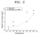
- FIG. 2 is a graph illustrating a radius of curvature of a silicon chip in response to a thickness change of the silicon chip
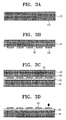
- FIGS. 3A to 3D are cross-sectional views for explaining a process of fabricating an active element
- FIGS. 4A to 4C are cross-sectional views for explaining a process of fabricating a flexible device
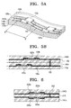
- FIG. 5A is a perspective view of a flexible device in accordance with another exemplary embodiment of the present invention.
- FIG. 5B is a cross-sectional view of a flexible device shown in FIG. 5A;
- FIG. 6 is a perspective view of a flexible device in accordance with another exemplary embodiment of the present invention.
- FIG. 7A is a cross-sectional view of a flexible pressure sensor in accordance with one exemplary embodiment of the present invention.
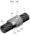
- FIG. 7B is a view illustrating a state that a blood vessel is surrounded by a flexible pressure sensor shown in FIG. 7A;
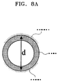
- FIG. 8A is a view for explaining a principle of measuring a blood pressure of a flexible pressure sensor
- FIG. 8B is a graph illustrating a resonance frequency change in response to a blood pressure change
- FIG. 9 is a concept view of a real time system of measuring a blood pressure.
- FIGS. 10A to 10E are cross-sectional views of process steps for explaining a process of fabricating a flexible pressure sensor.
- FIG. 1 A is a perspective view is a flexible device in accordance with one exemplary embodiment of the present invention
- FIG. 1B is a cross-sectional view taken along an electrical interconnection 130 within an A-A' range of the flexible device shown in FIG. 1A.
- the present flexible device has a first flexible substrate 110, a second flexible substrate 140, an active element 120, and an electrical interconnection 130.
- the active element 120 is attached on the first flexible substrate 110 and the electrical interconnection 130 is formed thereon, and the second flexible substrate 140 is deposited on the active element 120 and the electrical interconnection 130.
- the first flexible substrate 110 is one which has a flexibility, and is formed of a flexible material.
- the first flexible substrate 110 may be a substrate fabricated with a flexible high molecular material.
- polyimide may be applied as the high molecular material.
- the active element 120 is attached on the first flexible substrate 110.
- thermo-compression bonding, adhesive bonding, and so forth may be applied for a method of attaching the active element 120 on the substrate.
- a logic integrated circuit (IC), a central processing unit (CPU), a memory, a digital signal processor (DSP), a sensor, an actuator, a communication device and so forth may be applied for the active element 120.
- the kind of the active element 120 is not limited, so that other kinds besides the above-described examples may be applied for the active element 120.
- the active element 120 has a flexibility.
- the flexibility of the active element 120 aids in implementing the present flexible device.
- the active element 120 having the flexibility may be implemented by making its thickness thin.
- the active element 120 is generally implemented as a silicon chip.
- a thick silicon chip has hardly any flexibility (that is, it has a 'rigid' or 'brittle' property), however, it has a flexibility when a thickness of the silicon chip becomes thin (i.e. when it is decreased to a value of tens of •• or less).
- FIG. 2 is a graph illustrating a radius of curvature of the silicon chip in response to the thickness change, an "idealistic radius of curvature" (straight line) of the silicon chip, a "radius of curvature measured by computer simulation"(X mark), and an "actually measured radius of curvature” (• • mark) are shown in response to the thickness change in FIG. 2. Referring to FIG. 2, it can be seen that the radius of curvature is decreased when the thickness of the silicon chip becomes thinner. That is, it can be seen that the flexibility of the silicon chip is increased when the thickness becomes thinner.
- the thickness of the active element 120 may be made as thin as possible in order to allow the active element 120 have a flexibility. 50 ⁇ m is suitable for a thickness of the active element 120 in consideration of the current technique level. However, in consideration of a tendency that the thickness of the active elements becomes thinner, it will also be possible to implement the active element which has a far thinner thickness in the future.
- FIGS. 1A and 1B A description will be given with referring back to FIGS. 1A and 1B.
- An electrical interconnection 130 is formed on the first flexible substrate 110 for electrically interconnecting the active element 120.
- passive elements such as a resistor, an inductor, and a capacitor may be formed in the first flexible substrate 110.
- An insulator which is not shown, either, may also be formed in the first flexible substrate 110. In this case, the electrical interconnection, 130, the passive element, and the insulator may be formed such that they are thin and have flexibility.
- the second flexible substrate 140 is formed to be deposited on the active element 120 and the electrical interconnection 130.
- the second flexible substrate 140 is one which has a flexibility and is formed of a flexible material.
- the second flexible substrate 140 may be formed of the same material as the first flexible substrate 110. Accordingly, the second flexible substrate 140 may be implemented as a substrate formed of a flexible high molecular material, wherein polyimide may be applied for the high molecular material.
- the present flexible device also has flexibility.
- FIGS. 3A to 3D are cross-sectional views per process step for explaining a process of fabricating the active element 120.
- a plurality of active elements 120 are serially formed in a region (i.e. a bottom region of FIG. 3A) of a silicon wafer 20.
- the active element 120 is formed to have its thickness as thin as possible in order to allow the active element 120 to have the flexibility.
- Regions between the plurality of active elements 120 are then etched to form a plurality of grooves 25 as shown in FIG. 3B.
- a depth of the groove 25 is equal to a thickness of the active element 120. Any one between dry etching and wet etching may be employed for the etching method. Using wet etching helps to protect physical structures of the active elements 120.
- a tape 30 is then attached to the plurality of active elements 120 as shown in FIG. 3C, and a substrate 40 is attached to the tape 30.
- a thermal release tape may be employed for the tape 30.
- the silicon wafer 20 is then polished and removed as shown in FIG. 3D. Any one between physical polishing and chemical polishing may be employed for the polishing method. Using chemical polishing which uses a chemical material helps protect physical structures of the active elements 120.
- the plurality of active elements 120 is then removed from the tape 30 (in the direction of the arrow shown in FIG. 3D).
- FIGS. 3A to 3D A technique employing the process as shown in FIGS. 3A to 3D is instead introduced such that regions between the plurality of active elements 120 are wet etched to form a plurality of grooves 25 and the silicon wafer 20 is chemically polished to dice the plurality of active elements 120, because the active element 120 has a thin thickness (e.g. 50 ⁇ m or less) so that it is apt to be brittle or broken due to a vibration of the diamond wheel when sawing using the diamond wheel is carried out.
- a thin thickness e.g. 50 ⁇ m or less
- FIGS. 4A to 4C are cross-sectional views of steps for explaining a process of fabricating the flexible device
- An active element 120 having a flexibility is first attached on the first flexible substrate 110 having a flexibility as shown in FIG. 4A.
- thermo-compression bonding, adhesive bonding and so forth may be applied for a method of attaching the active element 120.
- An electrical interconnection 130 for electrically interconnecting the active element 120 is then formed on the first flexible substrate 110 as shown in FIG. 4B.
- Passive elements such as a resistor, an inductor and a capacitor, and an insulator may also be formed on the first flexible substrate 110 if necessary.
- the electrical interconnection 130, the passive element, and the insulator may be formed to have a thin thickness so that they have a flexibility.
- a second flexible substrate 140 having a flexibility is then deposited on the active element 120 and the electrical interconnection 130 as shown in FIG. 4C.
- the active element 120 having a flexibility, the flexible device having a flexibility, and a fabrication process thereof have been described up to now.
- the present flexible devices may be stacked to each other so that a resultant flexible device having a different structure may be implemented.
- FIG. 5A a perspective view of a flexible device having a different structure is shown such that the two flexible devices shown in FIG. 1A are stacked.
- FIG. 5B is a cross-sectional view of a flexible device shown in FIG. 5A which is taken along electrical interconnections 130a and 130b within a B-B' range.
- the flexible device shown in FIGS. 5A and 5B has a structure in which a flexible device having the first flexible substrate 110b, the active element 120b, the electrical interconnection 130b, and the second flexible substrate 140b are stacked on a flexible device having the first flexible substrate 110a, the active element 120a, the electrical interconnection 130a, and the second flexible substrate 140a.
- a passive element 150 is formed in the flexible substrates 110b and 140a.
- FIG. 6 a flexible device having a structure different from that of FIG. 5B is shown in FIG. 6. It can be seen from the flexible device shown in FIG. 6 that a passive element 250 is formed in the first flexible substrate 210, and active elements 220b and 220a are attached above and below the first flexible substrate 210, respectively and electrical interconnections 230b and 230a are respectively formed thereon, and the second flexible substrates 240a and 240b are deposited on the active elements 220a and 220b and the electrical interconnection 230a and 230b.
- the flexible pressure sensor has a flexibility, and may be fabricated to a have a fine-sized structure.
- the flexible pressure sensor may be implanted into the human body so that it may be used as a device for measuring a blood pressure.
- the present flexible pressure sensor will be described in detail assuming that the flexible pressure sensor is implanted into the human body to be used as a device for measuring a blood pressure.
- FIG. 7A is a cross-sectional view of the flexible pressure sensor in accordance with one exemplary embodiment of the present invention
- FIG. 7B is a view illustrating a state that a blood vessel is surrounded by the flexible pressure sensor shown in FIG. 7A.
- the present exemplary embodiment of the flexible pressure sensor has a first flexible substrate 310, first and second electrodes 320a and 320b, first and second wires 330a and 330b, a coil 335, and a second flexible substrate 340. Since the present flexible pressure sensor has a flexibility, it may have a circular shape when it is bent. Accordingly, the present flexible pressure sensor may surround the blood vessel 400.
- the first and second wires 330a and 330b are formed in the first flexible substrate 310, and the first and second electrodes 320a and 320b are formed below the wires, and the coil 335 is formed thereon, and the second flexible substrate 340 is deposited on the coil 335.
- the first flexible substrate 310 is one having a flexibility, and is preferably formed of a flexible high molecular material such as polyimide. Since the first flexible substrate 310 has flexibility, it may have a circular shape when it is bent.
- the first electrode 320a and the second electrode 320b are formed below the first flexible substrate 310 by a predetermined interval.
- the thickness of the first and second electrodes 320a and 320b may be made thin so that they have a flexibility.
- the first and second electrodes 320a and 320b may be formed of Gold (Au), which is harmless to the human body.
- the first flexible substrate 310 When the first flexible substrate 310 is bent to have a circular shape, the first electrode 320a and the second electrode 320b face each other. As a result, the first and second electrodes 320a and 320b constitute a capacitor. In this case, the blood vessel 400 and bloods flowing through the blood vessel 400 serve as a dielectric material.
- the coil 335 is formed on the first flexible substrate 310. In this case, the thickness of the coil 335 may be made thin so that it has a flexibility.
- the coil 335 may be formed of copper (Cu).
- the coil 335 is electrically connected to the first and second electrodes 320a and 320b through the first and second wires 330a and 330b. As such, when the 'capacitor formed by the first and second electrodes 320a and 320b' and the 'coil 335' are electrically connected to each other, an LC resonance circuit is formed. In the meantime, the coil 335 externally outputs a radio frequency (RF) signal corresponding to a resonance frequency of the LC resonance circuit.
- RF radio frequency
- the second flexible substrate 340 is deposited on the coil 335.
- the second flexible substrate 340 is one having a flexibility and may be formed of a flexible high molecular material such as polyimide. Since the second flexible substrate 320 has the flexibility, it may have a circular shape when it is bent.
- FIG. 8A is a view for explaining a principle of measuring a blood pressure of the present flexible pressure sensor.
- '••' indicates a dielectric rate of a dielectric material (i.e. the blood vessel 400 and the blood flowing through the blood vessel 400), and 's' indicates a cross-sectional area of the first electrode 320a or the second electrode 320b.
- the 'inter-electrode interval (d)' is equal to a 'diameter of the blood vessel 400'.
- the 'diameter of the blood vessel 400' changes in response to the 'blood pressure'. That is, the 'blood pressure' change causes the 'diameter of the blood vessel 400' to be changed, and the change of the 'diameter of the blood vessel 400' causes the 'inter-electrode interval (d)' to be changed, which causes the 'capacitance of the capacitor (C)' to be changed. Consequently, it can be understood that the change of the 'blood pressure' causes the 'capacitance of the capacitor (C)' to be changed.
- the 'L' indicates an inductance of the coil 335. According to the equation 2, it may be understood that the change of the 'capacitance (C) of the capacitor' causes the 'resonance frequency (F) of the LC resonance circuit' to be changed.
- the above-described description may be summarized as follows.
- the change of the 'blood pressure' • • change of the 'diameter of the blood vessel 400' • •change of the 'inter-electrode interval (d)' • •change of the 'capacitance (C) of the capacitor' • •change of the 'resonance frequency (F) of the LC resonance circuit' are sequentially progressed. Accordingly, it can be understood that the change of 'blood pressure' causes the 'resonance frequency (F) of the LC resonance circuit' to be changed.
- FIG. 8B is a graph illustrating the change of the resonance frequency change in response to the change of the blood pressure. Referring to FIG. 8B, it can be seen that the resonance frequency (F) is increased when the blood pressure is increased, and is decreased when the blood pressure is decreased.
- the coil externally outputs an RF signal corresponding to the resonance frequency (F) of the LC resonance circuit. Accordingly, information about the blood pressure is contained in the RF signal output from the coil 335.
- FIG. 9 shows a concept view of a real time system of measuring the blood pressure.
- the real time system of measuring the blood pressure may be implemented to have the above-described flexible pressure sensor 300 and a reader 400 which receives the RF signal output from the flexible pressure sensor 300 and analyzes the frequency of the signal.
- the reader 400 may be implemented so as to check the blood pressure by analyzing the frequency of the RF signal output from the flexible pressure sensor 300 and provide a warning sound when the blood pressure is not in a normal state.
- an emergency state of a patient may be immediately noticed when the flexible pressure sensor 300 is implanted into a body of the patient and the patient himself has the portable reader 400 or the reader is attached to a mobile phone.
- FIGS. 10A to 10E are cross-sectional views of several steps, for explaining a process of fabricating the flexible pressure sensor.
- a first electrode 320a is first formed below the first flexible substrate 310 having a flexibility as shown in FIG. 10A, and a second electrode 320b is formed to be spaced from the first electrode 320a by a predetermined interval.
- the second electrode 320b faces the first electrode 320a to be formed at position where a capacitor may be formed.
- the thickness of the first and second electrodes 320a and 320b may be made thin so that they have a flexibility, and the first and second electrodes 320a and 320b may be formed of Gold (Au), which is harmless to the human body.
- First and second wires 330a and 330b are formed in the first flexible substrate 310 as shown in FIG. 10B.
- the first and second wires 330a and 330b are formed to be electrically connected to the first and second electrodes 320a and 320b, respectively.
- a coil 335 is then formed on the first flexible substrate 310 as shown in FIG. 10C.
- the coil 335 is formed to be electrically connected to the first and second wires 330a and 330b. And the thickness of the coil 335 may be made thin so that it may have a flexibility.
- the coil 335 may be formed of copper (Cu).
- a second flexible substrate 340 having a flexibility is then deposited on the coil 335 as shown in FIG. 10D. Accordingly, the flexible pressure sensor shown in FIG. 7A is completed.
- a third flexible substrate 350 having a flexibility may be further deposited below the flexible pressure sensor (i.e. below the first and second electrodes 320a and 320b) shown in FIG. 10D.
- the flexible device having a high flexibility and the flexible pressure sensor as one kind of the flexible device may be implemented. They all have a high flexibility and may be fabricated to have a fine-sized structure, so that they may be applied for a medical treatment such as implantation to a living body, a human body and so forth.
- the flexible device has a high flexibility, so that it may be implanted to a curved surface, which contributes to removal of the limit of space where the semiconductor package device may be inserted.
- the present exemplary embodiments of the invention enables a user to select a print density level, to thereby properly change a print density based on an amount of a developing agent loaded in the developer so that images of good quality can be obtained all the time.
Landscapes
- Health & Medical Sciences (AREA)
- Child & Adolescent Psychology (AREA)
- Physics & Mathematics (AREA)
- General Physics & Mathematics (AREA)
- Measuring Fluid Pressure (AREA)
- Measuring Pulse, Heart Rate, Blood Pressure Or Blood Flow (AREA)
- Encapsulation Of And Coatings For Semiconductor Or Solid State Devices (AREA)
Abstract
A flexible device, a flexible pressure sensor, and a fabrication method thereof. The present flexible device includes: a first flexible substrate (210) formed of a flexible material to have a flexibility; an active element (220a,220b) formed to have a predetermined thickness and a flexibility, and being attached on the first flexible substrate; and a second flexible substrate (240a,240b) formed of a flexible material to have a flexibility, and being deposited on the active element. The flexible device and the flexible pressure sensor have a high flexibility, so that they may be applied for a medical treatment such as implantation to a living body, a human body and so forth, e.g. a blood vessel. In addition, the flexible device has a high flexibility, so that it may be inserted to a curved surface, which contributes to remove the limit of space where the semiconductor package device may be inserted.
Description
- This application claims priority under 35 U.S.C. § 119 from Korean Patent Application No. 2004-72630, filed on September 10, 2004, the entire content of which is incorporated herein by reference.
- The present invention relates to a semiconductor package device and a method of fabricating the same and, in particular, to a semiconductor package device in which a semiconductor device fabricated on a wafer is embedded and a method of fabricating the same.
- Semiconductor devices (e.g. chips) fabricated on a wafer are electrical devices, however, they may be not directly used by users and are apt to be broken. Accordingly, in order to use the semiconductor devices, they must be subjected to a packaging process for protection. The semiconductor devices fabricated on the wafer are subjected to the packaging process to be complete semiconductor package devices.
- The packaging process means a process of forming electrical interconnections in the semiconductor device and then molding it for preventing the semiconductor device from being damaged due to an external environment. The molding has a tendency to increase a thickness so as to prevent the semiconductor device from external impacts (e.g. thermal impact, mechanical impact), which acts as a cause of allowing a thickness of the semiconductor package device to be increased. In order to implement a small-sized semiconductor package device, it may be fabricated to be small and thin, however, which causes it to be readily broken, so that there exists a limit in making it small and thin.
- In recent years, attention has been paid to a medical technique of implanting the semiconductor package device to the human body to be used for medical treatment. To this end, the semiconductor package device must be supported by not only a small-sized feature but also a flexible feature.
- Accordingly, there exists a need for implementing a 'flexible semiconductor package device' (hereinafter, it will be referred to as a 'flexible device' for simplicity) which implants the flexible device to the human body or attaching it on any curved surface.
- It is therefore one object of the present invention to provide a flexible device having a high flexibility, a flexible pressure sensor, and a fabrication method thereof.
- According to one aspect of the present invention, there is provided a flexible device, which includes a first flexible substrate formed of a flexible material to have a flexibility; an active element formed to have a predetermined thickness and a flexibility, and being attached on the first flexible substrate; and a second flexible substrate formed of a flexible material to have a flexibility, and being deposited on the active element.
- The active element may be any one of a logic integrated circuit (IC), a central processing unit (CPU), a memory, a digital signal processor (DSP), a sensor, an actuator, and a communication device.
- In addition, a thickness of the active element may be 50 µm•or less.
- And the flexible device may further include another active element which is formed to have a predetermined thickness and a flexibility and is attached below the first flexible substrate.
- In addition, the flexible device may further include a passive element formed in the first flexible substrate. The passive element may be any one of a resistor, an inductor, and a capacitor.
- The first and second flexible substrates may be formed of a flexible high molecular material. And the high molecular material may be polyimide.
- According to other aspect of the present invention, there is provided a method of fabricating a flexible device, which includes: a) preparing an active element formed to have a predetermined thickness and a flexibility; b) attaching the active element on a first flexible substrate formed of a flexible material to have a flexibility; and c) depositing, on the active element, a second flexible substrate formed of a flexible material to have a flexibility.
- The a) step may include a1) forming a plurality of the active elements with a predetermined thickness on one region of a wafer; a2) etching regions between the active elements by the predetermined thickness; a3) attaching a tape to the active elements; a4) attaching a substrate to the tape; a5) polishing a region other than the one region of the wafer; and a6) preparing the active element by removing any one of the active elements attached to the tape from the tape.
- The a2) step may include performing wet etching on the regions between the active elements.
- The a5) step may include performing chemical polishing on the region other than the one region.
- In addition, the active element may have a thickness in a range of 50 µm or less.
- The b) step may include performing attaching the active element on the first flexible substrate using one method between thermo-compression bonding and adhesive bonding methods.
- The method may further include attaching another active element formed with a predetermined thickness to have a flexibility, below the first flexible substrate.
- And the method may further include forming a passive element in the first flexible substrate.
- According to another aspect of the present invention, there is provided a flexible pressure sensor, which includes a flexible substrate formed of a flexible material to have a flexibility, and allowing a circular shape to be formed when it is bent; a first electrode formed in one surface of the flexible substrate; a second electrode formed in the one surface of the flexible substrate, and facing the first electrode to form a capacitor when the flexible substrate is formed to have the circular shape; and a coil formed in the other surface of the flexible substrate, and forming a resonance circuit electrically connected to a capacitor formed by the first and second electrodes, and outputting a signal corresponding to a resonance frequency which changes in response to a change of a capacitance between the first electrode and the second electrode.
- The capacitance between the first electrode and the second electrode may change in response to a change of a diameter of a material interposed between the first electrode and the second electrode. In addition, the interposed material may be a blood vessel.
- The flexible pressure sensor may further include another flexible substrate formed of a flexible material to have a flexibility, allowing a circular shape to be formed when it is bent, and being deposited on the coil.
- The flexible substrate may be formed of a flexible high molecular material. And the high molecular material may be polyimide.
- The first and second electrodes may be formed of gold (Au) and the coil may be formed of copper (Cu).
- According to still another aspect of the present invention, there is provided a method of fabricating a flexible pressure sensor, which includes forming a first electrode in one surface of a flexible substrate, the flexible substrate being formed of a flexible material to have a flexibility and allowing a circular shape to be formed when it is bent; forming a second electrode formed in the one surface of the flexible substrate, and facing the first electrode to form a capacitor when the flexible substrate is formed to have the circular shape; and forming a coil in the other surface of the flexible substrate, the coil forming a resonance circuit electrically connected to a capacitor formed by the first and second electrodes and outputting a signal corresponding to a resonance frequency which changes in response to a change of a capacitance between the first electrode and the second electrode.
- The method may further include depositing another flexible substrate on the coil, the another flexible substrate being formed of a flexible material to have a flexibility and allowing a circular shape to be formed when it is bent.
- The above aspects and features of the present invention will be more apparent by describing exemplary embodiments of the present invention with reference to the accompanying drawings, in which:
- FIG. 1A is a perspective view of a flexible device in accordance with one exemplary embodiment of the present invention;
- FIG. 1B is a cross-sectional view of a flexible device shown in FIG. 1A;
- FIG. 2 is a graph illustrating a radius of curvature of a silicon chip in response to a thickness change of the silicon chip;
- [34] FIGS. 3A to 3D are cross-sectional views for explaining a process of fabricating an active element;
- FIGS. 4A to 4C are cross-sectional views for explaining a process of fabricating a flexible device;
- FIG. 5A is a perspective view of a flexible device in accordance with another exemplary embodiment of the present invention;
- FIG. 5B is a cross-sectional view of a flexible device shown in FIG. 5A;
- FIG. 6 is a perspective view of a flexible device in accordance with another exemplary embodiment of the present invention;
- FIG. 7A is a cross-sectional view of a flexible pressure sensor in accordance with one exemplary embodiment of the present invention;
- FIG. 7B is a view illustrating a state that a blood vessel is surrounded by a flexible pressure sensor shown in FIG. 7A;
- FIG. 8A is a view for explaining a principle of measuring a blood pressure of a flexible pressure sensor;
- FIG. 8B is a graph illustrating a resonance frequency change in response to a blood pressure change;
- FIG. 9 is a concept view of a real time system of measuring a blood pressure; and
- FIGS. 10A to 10E are cross-sectional views of process steps for explaining a process of fabricating a flexible pressure sensor.
- Hereinafter, exemplary embodiments of the present invention will be described in detail with reference to accompanying drawings. The described exemplary embodiments are intended to assist in the understanding of the invention, and are not intended to limit the scope of the invention in any way.
- FIG. 1 A is a perspective view is a flexible device in accordance with one exemplary embodiment of the present invention, and FIG. 1B is a cross-sectional view taken along an
electrical interconnection 130 within an A-A' range of the flexible device shown in FIG. 1A. Referring to FIGS. 1A and 1B, the present flexible device has a firstflexible substrate 110, a secondflexible substrate 140, anactive element 120, and anelectrical interconnection 130. Theactive element 120 is attached on the firstflexible substrate 110 and theelectrical interconnection 130 is formed thereon, and the secondflexible substrate 140 is deposited on theactive element 120 and theelectrical interconnection 130. - The first
flexible substrate 110 is one which has a flexibility, and is formed of a flexible material. In particular, the firstflexible substrate 110 may be a substrate fabricated with a flexible high molecular material. In this case, polyimide may be applied as the high molecular material. - The
active element 120 is attached on the firstflexible substrate 110. In this case, thermo-compression bonding, adhesive bonding, and so forth may be applied for a method of attaching theactive element 120 on the substrate. - A logic integrated circuit (IC), a central processing unit (CPU), a memory, a digital signal processor (DSP), a sensor, an actuator, a communication device and so forth may be applied for the
active element 120. However, the kind of theactive element 120 is not limited, so that other kinds besides the above-described examples may be applied for theactive element 120. - In the meantime, the
active element 120 has a flexibility. The flexibility of theactive element 120 aids in implementing the present flexible device. Theactive element 120 having the flexibility may be implemented by making its thickness thin. - The
active element 120 is generally implemented as a silicon chip. A thick silicon chip has hardly any flexibility (that is, it has a 'rigid' or 'brittle' property), however, it has a flexibility when a thickness of the silicon chip becomes thin (i.e. when it is decreased to a value of tens of •• or less). FIG. 2 is a graph illustrating a radius of curvature of the silicon chip in response to the thickness change, an "idealistic radius of curvature" (straight line) of the silicon chip, a "radius of curvature measured by computer simulation"(X mark), and an "actually measured radius of curvature" (• • mark) are shown in response to the thickness change in FIG. 2. Referring to FIG. 2, it can be seen that the radius of curvature is decreased when the thickness of the silicon chip becomes thinner. That is, it can be seen that the flexibility of the silicon chip is increased when the thickness becomes thinner. - The property that the flexibility is increased when the thickness of the material used to form the silicon chip is thinner as described above, may be equally applied to implementation of the present
active element 120. Accordingly, the thickness of theactive element 120 may be made as thin as possible in order to allow theactive element 120 have a flexibility. 50 µm is suitable for a thickness of theactive element 120 in consideration of the current technique level. However, in consideration of a tendency that the thickness of the active elements becomes thinner, it will also be possible to implement the active element which has a far thinner thickness in the future. - A description will be given with referring back to FIGS. 1A and 1B.
- An
electrical interconnection 130 is formed on the firstflexible substrate 110 for electrically interconnecting theactive element 120. Although not shown, passive elements such as a resistor, an inductor, and a capacitor may be formed in the firstflexible substrate 110. An insulator, which is not shown, either, may also be formed in the firstflexible substrate 110. In this case, the electrical interconnection, 130, the passive element, and the insulator may be formed such that they are thin and have flexibility. - The second
flexible substrate 140 is formed to be deposited on theactive element 120 and theelectrical interconnection 130. The secondflexible substrate 140 is one which has a flexibility and is formed of a flexible material. The secondflexible substrate 140 may be formed of the same material as the firstflexible substrate 110. Accordingly, the secondflexible substrate 140 may be implemented as a substrate formed of a flexible high molecular material, wherein polyimide may be applied for the high molecular material. - As mentioned above, all of the first
flexible substrate 110, theactive element 120, theelectrical interconnection 130, and the secondflexible substrate 140 which constitute the present flexible device, have flexibility. As a result, the present flexible device also has flexibility. - Hereinafter, a description of process of fabricating an
active element 120 having a flexibility and a process of fabricating a flexible device will be given in detail. A process of fabricating theactive element 120 having a flexibility is first described. FIGS. 3A to 3D are cross-sectional views per process step for explaining a process of fabricating theactive element 120. - As shown in FIG. 3A, a plurality of
active elements 120 are serially formed in a region (i.e. a bottom region of FIG. 3A) of asilicon wafer 20. In this case, theactive element 120 is formed to have its thickness as thin as possible in order to allow theactive element 120 to have the flexibility. In particular, it is preferable for theactive element 120 to have a thickness of 50 µm•or less. - Regions between the plurality of
active elements 120 are then etched to form a plurality ofgrooves 25 as shown in FIG. 3B. A depth of thegroove 25 is equal to a thickness of theactive element 120. Any one between dry etching and wet etching may be employed for the etching method. Using wet etching helps to protect physical structures of theactive elements 120. - A
tape 30 is then attached to the plurality ofactive elements 120 as shown in FIG. 3C, and asubstrate 40 is attached to thetape 30. In this case, a thermal release tape may be employed for thetape 30. - The
silicon wafer 20 is then polished and removed as shown in FIG. 3D. Any one between physical polishing and chemical polishing may be employed for the polishing method. Using chemical polishing which uses a chemical material helps protect physical structures of theactive elements 120. - The plurality of
active elements 120 is then removed from the tape 30 (in the direction of the arrow shown in FIG. 3D). - Sawing using a diamond wheel is not employed in a process of fabricating the present
active element 120. A technique employing the process as shown in FIGS. 3A to 3D is instead introduced such that regions between the plurality ofactive elements 120 are wet etched to form a plurality ofgrooves 25 and thesilicon wafer 20 is chemically polished to dice the plurality ofactive elements 120, because theactive element 120 has a thin thickness (e.g. 50 µm or less) so that it is apt to be brittle or broken due to a vibration of the diamond wheel when sawing using the diamond wheel is carried out. - Hereinafter, a process of fabricating a flexible device will be described in detail. FIGS. 4A to 4C are cross-sectional views of steps for explaining a process of fabricating the flexible device
- An
active element 120 having a flexibility is first attached on the firstflexible substrate 110 having a flexibility as shown in FIG. 4A. In this case, thermo-compression bonding, adhesive bonding and so forth may be applied for a method of attaching theactive element 120. - An
electrical interconnection 130 for electrically interconnecting theactive element 120 is then formed on the firstflexible substrate 110 as shown in FIG. 4B. Passive elements such as a resistor, an inductor and a capacitor, and an insulator may also be formed on the firstflexible substrate 110 if necessary. Theelectrical interconnection 130, the passive element, and the insulator may be formed to have a thin thickness so that they have a flexibility. - A second
flexible substrate 140 having a flexibility is then deposited on theactive element 120 and theelectrical interconnection 130 as shown in FIG. 4C. - The
active element 120 having a flexibility, the flexible device having a flexibility, and a fabrication process thereof have been described up to now. - The present flexible devices may be stacked to each other so that a resultant flexible device having a different structure may be implemented. Referring to FIG. 5A, a perspective view of a flexible device having a different structure is shown such that the two flexible devices shown in FIG. 1A are stacked. And FIG. 5B is a cross-sectional view of a flexible device shown in FIG. 5A which is taken along
electrical interconnections - It can be seen that the flexible device shown in FIGS. 5A and 5B has a structure in which a flexible device having the first
flexible substrate 110b, theactive element 120b, theelectrical interconnection 130b, and the secondflexible substrate 140b are stacked on a flexible device having the firstflexible substrate 110a, theactive element 120a, theelectrical interconnection 130a, and the secondflexible substrate 140a. In addition, it can be seen that apassive element 150 is formed in theflexible substrates - Alternatively, a flexible device having a structure different from that of FIG. 5B is shown in FIG. 6. It can be seen from the flexible device shown in FIG. 6 that a
passive element 250 is formed in the firstflexible substrate 210, andactive elements flexible substrate 210, respectively andelectrical interconnections flexible substrates active elements electrical interconnection - Hereinafter, a flexible pressure sensor as one kind of the flexible device will be described. The flexible pressure sensor has a flexibility, and may be fabricated to a have a fine-sized structure. In this case, the flexible pressure sensor may be implanted into the human body so that it may be used as a device for measuring a blood pressure. Hereinafter, the present flexible pressure sensor will be described in detail assuming that the flexible pressure sensor is implanted into the human body to be used as a device for measuring a blood pressure.
- FIG. 7A is a cross-sectional view of the flexible pressure sensor in accordance with one exemplary embodiment of the present invention, and FIG. 7B is a view illustrating a state that a blood vessel is surrounded by the flexible pressure sensor shown in FIG. 7A.
- Referring to FIGS. 7A and 7B, the present exemplary embodiment of the flexible pressure sensor has a first
flexible substrate 310, first andsecond electrodes second wires coil 335, and a secondflexible substrate 340. Since the present flexible pressure sensor has a flexibility, it may have a circular shape when it is bent. Accordingly, the present flexible pressure sensor may surround theblood vessel 400. - The first and
second wires flexible substrate 310, and the first andsecond electrodes coil 335 is formed thereon, and the secondflexible substrate 340 is deposited on thecoil 335. - The first
flexible substrate 310 is one having a flexibility, and is preferably formed of a flexible high molecular material such as polyimide. Since the firstflexible substrate 310 has flexibility, it may have a circular shape when it is bent. - The
first electrode 320a and thesecond electrode 320b are formed below the firstflexible substrate 310 by a predetermined interval. In this case, the thickness of the first andsecond electrodes second electrodes - When the first
flexible substrate 310 is bent to have a circular shape, thefirst electrode 320a and thesecond electrode 320b face each other. As a result, the first andsecond electrodes blood vessel 400 and bloods flowing through theblood vessel 400 serve as a dielectric material. - The
coil 335 is formed on the firstflexible substrate 310. In this case, the thickness of thecoil 335 may be made thin so that it has a flexibility. Thecoil 335 may be formed of copper (Cu). - The
coil 335 is electrically connected to the first andsecond electrodes second wires second electrodes coil 335 externally outputs a radio frequency (RF) signal corresponding to a resonance frequency of the LC resonance circuit. - The second
flexible substrate 340 is deposited on thecoil 335. The secondflexible substrate 340 is one having a flexibility and may be formed of a flexible high molecular material such as polyimide. Since the second flexible substrate 320 has the flexibility, it may have a circular shape when it is bent. - Hereinafter, a principle of measuring the blood pressure of the present flexible pressure sensor will be described in detail with reference to FIGS. 8A and 8B.
- FIG. 8A is a view for explaining a principle of measuring a blood pressure of the present flexible pressure sensor. A capacitance (C) of the 'capacitor formed by the
first electrode 320a and thesecond electrode 320b' (hereinafter, it will be referred to as a capacitor for simplicity) is inverse proportion to the 'interval between thefirst electrode 320a and thesecond electrode 320b' (d) (hereinafter, it will be referred to an 'inter-electrode interval' for simplicity). This may be expressed as theequation 1 below:
- Wherein '••' indicates a dielectric rate of a dielectric material (i.e. the
blood vessel 400 and the blood flowing through the blood vessel 400), and 's' indicates a cross-sectional area of thefirst electrode 320a or thesecond electrode 320b. - The 'inter-electrode interval (d)' is equal to a 'diameter of the blood vessel 400'. The 'diameter of the blood vessel 400' changes in response to the 'blood pressure'. That is, the 'blood pressure' change causes the 'diameter of the blood vessel 400' to be changed, and the change of the 'diameter of the blood vessel 400' causes the 'inter-electrode interval (d)' to be changed, which causes the 'capacitance of the capacitor (C)' to be changed. Consequently, it can be understood that the change of the 'blood pressure' causes the 'capacitance of the capacitor (C)' to be changed.
- In the meantime, a resonance frequency (F) of the 'LC resonance circuit formed by the
coil 335 and the capacitor' (hereinafter, it will be referred to as an 'LC resonance circuit' for simplicity) may be expressed as the equation 2 below:
- Wherein, the 'L' indicates an inductance of the
coil 335. According to the equation 2, it may be understood that the change of the 'capacitance (C) of the capacitor' causes the 'resonance frequency (F) of the LC resonance circuit' to be changed. - The above-described description may be summarized as follows. The change of the 'blood pressure' • • change of the 'diameter of the blood vessel 400' • •change of the 'inter-electrode interval (d)' • •change of the 'capacitance (C) of the capacitor' • •change of the 'resonance frequency (F) of the LC resonance circuit' are sequentially progressed. Accordingly, it can be understood that the change of 'blood pressure' causes the 'resonance frequency (F) of the LC resonance circuit' to be changed.
- FIG. 8B is a graph illustrating the change of the resonance frequency change in response to the change of the blood pressure. Referring to FIG. 8B, it can be seen that the resonance frequency (F) is increased when the blood pressure is increased, and is decreased when the blood pressure is decreased.
- As mentioned above, the coil externally outputs an RF signal corresponding to the resonance frequency (F) of the LC resonance circuit. Accordingly, information about the blood pressure is contained in the RF signal output from the
coil 335. - When the RF signal output from the
coil 335 is received and the frequency of the signal is analyzed, the information about the blood pressure may be obtained. And the blood pressure may be measured in real time when the RF signal is output and analyzed in real time. FIG. 9 shows a concept view of a real time system of measuring the blood pressure. - The real time system of measuring the blood pressure may be implemented to have the above-described
flexible pressure sensor 300 and areader 400 which receives the RF signal output from theflexible pressure sensor 300 and analyzes the frequency of the signal. Thereader 400 may be implemented so as to check the blood pressure by analyzing the frequency of the RF signal output from theflexible pressure sensor 300 and provide a warning sound when the blood pressure is not in a normal state. - Regarding cases having cardio and/or vascular problems, an emergency state of a patient may be immediately noticed when the
flexible pressure sensor 300 is implanted into a body of the patient and the patient himself has theportable reader 400 or the reader is attached to a mobile phone. - Hereinafter, a process of fabricating the flexible pressure sensor shown in FIG. 7A will be described in detail. FIGS. 10A to 10E are cross-sectional views of several steps, for explaining a process of fabricating the flexible pressure sensor.
- A
first electrode 320a is first formed below the firstflexible substrate 310 having a flexibility as shown in FIG. 10A, and asecond electrode 320b is formed to be spaced from thefirst electrode 320a by a predetermined interval. In this case, when the firstflexible substrate 310 is bent to have a circular shape, thesecond electrode 320b faces thefirst electrode 320a to be formed at position where a capacitor may be formed. - In this case, the thickness of the first and
second electrodes second electrodes - First and
second wires flexible substrate 310 as shown in FIG. 10B. In this case, the first andsecond wires second electrodes - A
coil 335 is then formed on the firstflexible substrate 310 as shown in FIG. 10C. In this case, thecoil 335 is formed to be electrically connected to the first andsecond wires coil 335 may be made thin so that it may have a flexibility. Thecoil 335 may be formed of copper (Cu). - A second
flexible substrate 340 having a flexibility is then deposited on thecoil 335 as shown in FIG. 10D. Accordingly, the flexible pressure sensor shown in FIG. 7A is completed. - In the meantime, as shown in FIG. 10E, a third
flexible substrate 350 having a flexibility may be further deposited below the flexible pressure sensor (i.e. below the first andsecond electrodes - As mentioned above, according to an exemplary embodiment of the present invention, the flexible device having a high flexibility and the flexible pressure sensor as one kind of the flexible device may be implemented. They all have a high flexibility and may be fabricated to have a fine-sized structure, so that they may be applied for a medical treatment such as implantation to a living body, a human body and so forth. In addition, the flexible device has a high flexibility, so that it may be implanted to a curved surface, which contributes to removal of the limit of space where the semiconductor package device may be inserted.
- The present exemplary embodiments of the invention enables a user to select a print density level, to thereby properly change a print density based on an amount of a developing agent loaded in the developer so that images of good quality can be obtained all the time.
- The foregoing exemplary embodiments and advantages are merely exemplary and are not to be construed as limiting the present invention. The present teaching can be readily applied to other types of apparatuses. Also, the description of the exemplary embodiments of the present invention is intended to be illustrative, and not to limit the scope of the claims, and many alternatives, modifications, and variations will be apparent to those skilled in the art.
Claims (26)
- A flexible device, comprising:a first flexible substrate formed of a flexible material to have a flexibility;an active element formed to have a predetermined thickness and a flexibility, and being attached on the first flexible substrate; anda second flexible substrate formed of a flexible material to have a flexibility, and being deposited on the active element.
- The flexible device as claimed in claim 1, wherein the active element comprises at least one of a logic integrated circuit (IC), a central processing unit (CPU), a memory, a digital signal processor (DSP), a sensor, an actuator, and a communication device.
- The flexible device as claimed in claim 1, wherein a thickness of the active element is 50 µm•or less.
- The flexible device as claimed in claim 1, further comprising:another active element formed to have a predetermined thickness and a flexibility, and being attached below the first flexible substrate.
- The flexible device as claimed in claim 1, further comprising:a passive element formed in the first flexible substrate.
- The flexible device as claimed in claim 5, wherein the passive element comprises at least one of a resistor, an inductor, and a capacitor.
- The flexible device as claimed in claim 1, wherein the first and second flexible substrates are formed of a flexible high molecular material.
- The flexible device as claimed in claim 7, wherein the high molecular material is polyimide.
- A method of fabricating a flexible device, comprising:a) preparing an active element formed to have a predetermined thickness and a flexibility;b) attaching the active element on a first flexible substrate formed of a flexible material to have a flexibility; andc) depositing, on the active element, a second flexible substrate formed of a flexible material to have a flexibility.
- The method as claimed in claim 9, wherein the a) step includes:a1) forming a plurality of the active elements with the predetermined thickness on one region of a wafer;a2) etching regions between the active elements by the predetermined thickness;a3) attaching a tape to the active elements;a4) attaching a substrate to the tape;a5) polishing a region other than the one region of the wafer; anda6) preparing the active element by removing any one of the active elements attached to the tape from the tape.
- The method as claimed in claim 10, wherein the a2) step comprises wet etching on the regions between the active elements.
- The method as claimed in claim 10, wherein the a5) step comprises performing chemical polishing on the region other than the one region.
- The method as claimed in claim 10, wherein the predetermined thickness of the active element is 50 µm or less.
- The method as claimed in claim 9, wherein the b) step comprises attaching the active element on the first flexible substrate using at least one of thermo-compression bonding and adhesive bonding methods.
- The method as claimed in claim 9, further comprising:attaching another active element formed with a predetermined thickness to have a flexibility, below the first flexible substrate.
- The method as claimed in claim 9, further comprising:forming a passive element in the first flexible substrate.
- A flexible pressure sensor, comprising:a flexible substrate formed of a flexible material to have a flexibility, and allowing a circular shape to be formed when it is bent;a first electrode formed in one surface of the flexible substrate;a second electrode formed in the one surface of the flexible substrate, and facing the first electrode to form a capacitor when the flexible substrate is formed to have the circular shape; anda coil formed in the other surface of the flexible substrate, and forming a resonance circuit electrically connected to a capacitor formed by the first and second electrodes, and outputting a signal corresponding to a resonance frequency which changes in response to a change of a capacitance between the first electrode and the second electrode.
- The flexible pressure sensor as claimed in claim 17, wherein the capacitance between the first electrode and the second electrode changes in response to a change of a diameter of a material interposed between the first electrode and the second electrode.
- The flexible pressure sensor as claimed in claim 18, wherein the interposed material is a blood vessel.
- The flexible pressure sensor as claimed in claim 17, further comprising:another flexible substrate formed of a flexible material to have a flexibility, allowing a circular shape to be formed when it is bent, and being deposited on the coil.
- The flexible pressure sensor as claimed in claim 17, wherein the flexible substrate is formed of a flexible high molecular material.
- The flexible pressure sensor as claimed in claim 21, wherein the high molecular material is polyimide.
- The flexible pressure sensor as claimed in claim 17, wherein the first and second electrodes are formed of gold (Au).
- The flexible pressure sensor as claimed in claim 17, wherein the coil is formed of copper (Cu).
- A method of fabricating a flexible pressure sensor, comprising:forming a first electrode in one surface of a flexible substrate, the flexible substrate being formed of a flexible material to have a flexibility and allowing a circular shape to be formed when it is bent;forming a second electrode formed in the one surface of the flexible substrate, and facing the first electrode to form a capacitor when the flexible substrate is formed to have the circular shape; andforming a coil in the other surface of the flexible substrate, the coil forming a resonance circuit electrically connected to a capacitor formed by the first and second electrodes and outputting a signal corresponding to a resonance frequency which changes in response to a change of a capacitance between the first electrode and the second electrode.
- The method as claimed in claim 25, further comprising:depositing another flexible substrate on the coil, the another flexible substrate being formed of a flexible material to have a flexibility and allowing a circular shape to be formed when it is bent.
Applications Claiming Priority (1)
| Application Number | Priority Date | Filing Date | Title |
|---|---|---|---|
| KR1020040072630A KR100643756B1 (en) | 2004-09-10 | 2004-09-10 | Flexible element, flexible pressure sensor, and manufacturing method thereof |
Publications (1)
| Publication Number | Publication Date |
|---|---|
| EP1635158A2 true EP1635158A2 (en) | 2006-03-15 |
Family
ID=36377953
Family Applications (1)
| Application Number | Title | Priority Date | Filing Date |
|---|---|---|---|
| EP05019262A Withdrawn EP1635158A2 (en) | 2004-09-10 | 2005-09-05 | Flexible device, flexible pressure sensor, and fabrication method thereof |
Country Status (4)
| Country | Link |
|---|---|
| US (2) | US20060056161A1 (en) |
| EP (1) | EP1635158A2 (en) |
| JP (2) | JP2006108657A (en) |
| KR (1) | KR100643756B1 (en) |
Cited By (10)
| Publication number | Priority date | Publication date | Assignee | Title |
|---|---|---|---|---|
| WO2006122750A1 (en) * | 2005-05-19 | 2006-11-23 | Universitätsklinikum Freiburg | Implantable blood pressure sensor |
| WO2007051110A3 (en) * | 2005-10-24 | 2007-08-23 | Checkpoint Systems Inc | Wire embedded bridge |
| DE102006057384A1 (en) * | 2006-12-04 | 2008-06-05 | Micronas Gmbh | Semiconductor component manufacturing method, involves pivoting and/or tilting and/or rotating sensors relative to each other with plane under bending deformation of area, where sensors are displaced parallel to each other with plane |
| WO2009131879A1 (en) | 2008-04-25 | 2009-10-29 | Medtronic, Inc. | Implantable device and method for monitoring venous diameter |
| DE102010010348A1 (en) | 2010-03-05 | 2011-09-08 | Albert-Ludwigs-Universität Freiburg | Implantable device for detecting a vessel wall strain |
| FR2967774A1 (en) * | 2010-11-24 | 2012-05-25 | Nanomade Concept | MINIATURIZED PRESSURE SENSOR |
| WO2017199148A1 (en) * | 2016-05-16 | 2017-11-23 | King Abdullah University Of Science And Technology | Decal electronics for printed high performance cmos electronic systems |
| CN107405112A (en) * | 2015-03-13 | 2017-11-28 | 威里利生命科学有限责任公司 | User interaction for bandage-type monitoring devices |
| CN110613449A (en) * | 2019-09-23 | 2019-12-27 | 清华大学 | Degradable flexible blood vessel detection device and system |
| CN112326097A (en) * | 2020-09-29 | 2021-02-05 | 浙江清华柔性电子技术研究院 | Flexible pressure sensor and preparation method thereof |
Families Citing this family (86)
| Publication number | Priority date | Publication date | Assignee | Title |
|---|---|---|---|---|
| GB0505826D0 (en) * | 2005-03-22 | 2005-04-27 | Uni Microelektronica Ct Vsw | Methods for embedding of conducting material and devices resulting from said methods |
| US8701469B2 (en) * | 2006-11-21 | 2014-04-22 | Cornell University | Flexible substrate sensor system for environmental and infrastructure monitoring |
| KR100829385B1 (en) * | 2006-11-27 | 2008-05-13 | 동부일렉트로닉스 주식회사 | Semiconductor device and method of manufacturing the same |
| EP2349440B1 (en) | 2008-10-07 | 2019-08-21 | Mc10, Inc. | Catheter balloon having stretchable integrated circuitry and sensor array |
| US9123614B2 (en) | 2008-10-07 | 2015-09-01 | Mc10, Inc. | Methods and applications of non-planar imaging arrays |
| US8389862B2 (en) * | 2008-10-07 | 2013-03-05 | Mc10, Inc. | Extremely stretchable electronics |
| US8886334B2 (en) * | 2008-10-07 | 2014-11-11 | Mc10, Inc. | Systems, methods, and devices using stretchable or flexible electronics for medical applications |
| US8097926B2 (en) | 2008-10-07 | 2012-01-17 | Mc10, Inc. | Systems, methods, and devices having stretchable integrated circuitry for sensing and delivering therapy |
| US8372726B2 (en) * | 2008-10-07 | 2013-02-12 | Mc10, Inc. | Methods and applications of non-planar imaging arrays |
| EP2200412A1 (en) | 2008-12-17 | 2010-06-23 | Nederlandse Organisatie voor toegepast-natuurwetenschappelijk Onderzoek TNO | Flexible electronic product and method for manufacturing the same |
| WO2010086033A1 (en) * | 2009-01-30 | 2010-08-05 | Interuniversitair Microelektronica Centrum Vzw | Stretchable electronic device |
| KR101073633B1 (en) * | 2009-07-06 | 2011-10-14 | 한국과학기술원 | method for manufacturing flexible sensor, flexible sensor manufactured by the same |
| KR101282204B1 (en) * | 2009-09-25 | 2013-07-04 | 이홍희 | Secondary battery and fabrication method thereof |
| US20110218756A1 (en) * | 2009-10-01 | 2011-09-08 | Mc10, Inc. | Methods and apparatus for conformal sensing of force and/or acceleration at a person's head |
| WO2011041727A1 (en) | 2009-10-01 | 2011-04-07 | Mc10, Inc. | Protective cases with integrated electronics |
| KR101042241B1 (en) * | 2009-10-08 | 2011-06-17 | 한국과학기술원 | Flexible secondary battery manufacturing method, a flexible secondary battery manufactured according to |
| US9078361B2 (en) * | 2010-01-29 | 2015-07-07 | Nederlandse Organisatie Voor Toegepast-Natuurwetenschappelijk Onderzoek Tno | Assembly, component for an assembly and method of manufacturing an assembly |
| WO2012109039A1 (en) * | 2011-01-30 | 2012-08-16 | Warnking Reinhard J | System for detection of blood pressure using a pressure sensing guide wire |
| US9159635B2 (en) | 2011-05-27 | 2015-10-13 | Mc10, Inc. | Flexible electronic structure |
| US9757050B2 (en) | 2011-08-05 | 2017-09-12 | Mc10, Inc. | Catheter balloon employing force sensing elements |
| WO2013022853A1 (en) | 2011-08-05 | 2013-02-14 | Mc10, Inc. | Catheter balloon methods and apparatus employing sensing elements |
| US20130200268A1 (en) * | 2011-09-28 | 2013-08-08 | Mc10, Inc. | Electronics for detection of a property of a surface |
| US20130229776A1 (en) * | 2011-12-23 | 2013-09-05 | Wisconsin Alumni Research Foundation | High-speed, flexible integrated circuits and methods for making high-speed, flexible integrated circuits |
| KR101451887B1 (en) * | 2012-04-26 | 2014-10-16 | 하나 마이크론(주) | Integrated circuit device package and method for manufacturing the same |
| BR112014026170A2 (en) | 2012-04-26 | 2017-07-18 | Hana Micron Co Ltd | integrated circuit device packages and methods of manufacturing integrated circuit device packages |
| US9226402B2 (en) | 2012-06-11 | 2015-12-29 | Mc10, Inc. | Strain isolation structures for stretchable electronics |
| US9295842B2 (en) | 2012-07-05 | 2016-03-29 | Mc10, Inc. | Catheter or guidewire device including flow sensing and use thereof |
| EP2866645A4 (en) | 2012-07-05 | 2016-03-30 | Mc10 Inc | CATHETER DEVICE COMPRISING A FLOW DETECTOR |
| US9171794B2 (en) | 2012-10-09 | 2015-10-27 | Mc10, Inc. | Embedding thin chips in polymer |
| CN105008949A (en) | 2012-10-09 | 2015-10-28 | Mc10股份有限公司 | Conformal electronics integrated with apparel |
| US20140131897A1 (en) | 2012-11-15 | 2014-05-15 | Taiwan Semiconductor Manufacturing Company, Ltd. | Warpage Control for Flexible Substrates |
| CN105308745A (en) | 2012-12-12 | 2016-02-03 | 哈纳米克罗恩公司 | Memory card systems comprising flexible integrated circuit element packages, and methods for manufacturing said memory card systems |
| US9706647B2 (en) | 2013-05-14 | 2017-07-11 | Mc10, Inc. | Conformal electronics including nested serpentine interconnects |
| US9372123B2 (en) | 2013-08-05 | 2016-06-21 | Mc10, Inc. | Flexible temperature sensor including conformable electronics |
| KR102022322B1 (en) * | 2013-10-01 | 2019-09-18 | 엘지디스플레이 주식회사 | Flexible device and method for detecting bending of the same |
| KR20160065948A (en) | 2013-10-07 | 2016-06-09 | 엠씨10, 인크 | Conformal sensor systems for sensing and analysis |
| EP3071096A4 (en) | 2013-11-22 | 2017-08-09 | Mc10, Inc. | Conformal sensor systems for sensing and analysis of cardiac activity |
| US10410962B2 (en) | 2014-01-06 | 2019-09-10 | Mc10, Inc. | Encapsulated conformal electronic systems and devices, and methods of making and using the same |
| CN106063392B (en) | 2014-03-04 | 2020-06-02 | Mc10股份有限公司 | Multi-part flexible enclosure for electronic devices |
| KR101634765B1 (en) * | 2014-05-23 | 2016-06-28 | 하나 마이크론(주) | Integrated circuit device package and Wire bonding type package and Flip bonding type package having the same |
| KR102250188B1 (en) | 2014-07-04 | 2021-05-10 | 삼성전자주식회사 | Apparatus for detecting information of the living body |
| KR102284652B1 (en) * | 2014-08-28 | 2021-08-02 | 삼성전자 주식회사 | Semiconductor package |
| US9899330B2 (en) * | 2014-10-03 | 2018-02-20 | Mc10, Inc. | Flexible electronic circuits with embedded integrated circuit die |
| US10297572B2 (en) | 2014-10-06 | 2019-05-21 | Mc10, Inc. | Discrete flexible interconnects for modules of integrated circuits |
| USD781270S1 (en) | 2014-10-15 | 2017-03-14 | Mc10, Inc. | Electronic device having antenna |
| CN107113960A (en) * | 2014-12-08 | 2017-08-29 | 株式会社藤仓 | Retractility substrate |
| KR101667203B1 (en) * | 2015-01-14 | 2016-10-18 | 전남대학교산학협력단 | manufacture method of pressure sensor for blood vessel, pressure sensor produced by the same and stent having same pressure sensor |
| US12465324B2 (en) | 2015-02-12 | 2025-11-11 | Foundry Innovation & Research 1, Ltd. | Patient fluid management systems and methods employing integrated fluid status sensing |
| EP3256043B1 (en) | 2015-02-12 | 2020-03-18 | Foundry Innovation & Research 1, Ltd. | Implantable devices for heart failure monitoring |
| EP3258837A4 (en) | 2015-02-20 | 2018-10-10 | Mc10, Inc. | Automated detection and configuration of wearable devices based on on-body status, location, and/or orientation |
| WO2016140961A1 (en) | 2015-03-02 | 2016-09-09 | Mc10, Inc. | Perspiration sensor |
| US9439326B1 (en) * | 2015-05-28 | 2016-09-06 | Hana Micron, Inc. | Electronic components |
| US10653332B2 (en) | 2015-07-17 | 2020-05-19 | Mc10, Inc. | Conductive stiffener, method of making a conductive stiffener, and conductive adhesive and encapsulation layers |
| US11039813B2 (en) | 2015-08-03 | 2021-06-22 | Foundry Innovation & Research 1, Ltd. | Devices and methods for measurement of Vena Cava dimensions, pressure and oxygen saturation |
| WO2017031129A1 (en) | 2015-08-19 | 2017-02-23 | Mc10, Inc. | Wearable heat flux devices and methods of use |
| WO2017059215A1 (en) | 2015-10-01 | 2017-04-06 | Mc10, Inc. | Method and system for interacting with a virtual environment |
| CN108289630A (en) | 2015-10-05 | 2018-07-17 | Mc10股份有限公司 | Method and system for nerve modulation and stimulation |
| US11243127B2 (en) | 2016-02-03 | 2022-02-08 | Hutchinson Technology Incorporated | Miniature pressure/force sensor with integrated leads |
| CN108781313B (en) | 2016-02-22 | 2022-04-08 | 美谛达解决方案公司 | Systems, devices, and methods for coupled hubs and sensor nodes for on-body acquisition of sensor information |
| WO2017147052A1 (en) | 2016-02-22 | 2017-08-31 | Mc10, Inc. | System, devices, and method for on-body data and power transmission |
| EP3435855B1 (en) | 2016-03-29 | 2023-05-10 | The Board of Trustees of the Leland Stanford Junior University | Proximity sensor circuits and related sensing methods |
| US11154235B2 (en) | 2016-04-19 | 2021-10-26 | Medidata Solutions, Inc. | Method and system for measuring perspiration |
| WO2017204610A1 (en) * | 2016-05-27 | 2017-11-30 | 주식회사 토닥 | Bio-implantable device and method for manufacturing same |
| US11701018B2 (en) | 2016-08-11 | 2023-07-18 | Foundry Innovation & Research 1, Ltd. | Wireless resonant circuit and variable inductance vascular monitoring implants and anchoring structures therefore |
| US11206992B2 (en) | 2016-08-11 | 2021-12-28 | Foundry Innovation & Research 1, Ltd. | Wireless resonant circuit and variable inductance vascular monitoring implants and anchoring structures therefore |
| EP3496606A1 (en) | 2016-08-11 | 2019-06-19 | Foundry Innovation & Research 1, Ltd. | Systems and methods for patient fluid management |
| US10447347B2 (en) | 2016-08-12 | 2019-10-15 | Mc10, Inc. | Wireless charger and high speed data off-loader |
| EP3463082B1 (en) | 2016-11-29 | 2020-07-29 | Foundry Innovation & Research 1, Ltd. | Wireless resonant circuit and variable inductance vascular implants for monitoring patient vasculature system |
| US10523258B2 (en) * | 2017-03-06 | 2019-12-31 | Samsung Electronics Co., Ltd. | Communication device to perform wireless communication and wireless power transfer, and electrode device to transmit and receive electrical signal from target |
| US11944495B2 (en) | 2017-05-31 | 2024-04-02 | Foundry Innovation & Research 1, Ltd. | Implantable ultrasonic vascular sensor |
| WO2018220146A1 (en) | 2017-05-31 | 2018-12-06 | Foundry Innovation & Research 1, Ltd. | Implantable sensors for vascular monitoring |
| CN111610892B (en) * | 2017-06-30 | 2023-08-11 | 武汉天马微电子有限公司 | A display substrate, display panel and display device |
| KR101928478B1 (en) * | 2017-07-28 | 2018-12-12 | 주식회사 신우전자 | Electrochemical gas sensor having flexible curved electrode |
| JP6791101B2 (en) * | 2017-11-15 | 2020-11-25 | オムロン株式会社 | Capacitive pressure sensor |
| JP6773007B2 (en) * | 2017-11-15 | 2020-10-21 | オムロン株式会社 | Capacitive pressure sensor |
| KR102214226B1 (en) * | 2018-01-26 | 2021-02-09 | 성균관대학교산학협력단 | Piezoresistive-type flexible sensor including laminated rlc and preparing method thereof |
| US12672848B2 (en) | 2018-02-02 | 2026-07-07 | Foundry Innovation & Research 1, Ltd. | Dialysis catheters with integrated fluid status sensing and related systems and methods |
| WO2019169277A1 (en) * | 2018-03-02 | 2019-09-06 | The United States Government As Represented By The United States Department Of Veterans Affairs | Devices and systems for treatment of urinary incontinence, and methods of making and using same |
| US11638353B2 (en) * | 2018-09-17 | 2023-04-25 | Hutchinson Technology Incorporated | Apparatus and method for forming sensors with integrated electrical circuits on a substrate |
| WO2020087026A1 (en) * | 2018-10-25 | 2020-04-30 | The Board Of Trustees Of The Leland Stanford Junior University | Inductor-capacitor based sensor apparatuses |
| KR102728514B1 (en) * | 2018-11-27 | 2024-11-12 | 삼성전자주식회사 | Living body information detecting apparatus |
| KR102217305B1 (en) * | 2019-03-19 | 2021-02-19 | 한국과학기술원 | Flexible sensor based single crystal silicon and method for making the flexible sensor |
| CN111232914B (en) * | 2020-01-14 | 2025-11-28 | 浙江清华柔性电子技术研究院 | Flexible graphene joint sensor and preparation method thereof |
| KR102342513B1 (en) * | 2020-07-23 | 2021-12-23 | (주)실리콘인사이드 | Force sensor and earphone including the same |
| AU2021340898B2 (en) * | 2020-09-14 | 2024-07-11 | Case Western Reserve University | Flexible pressure sensor with wireless monitoring capability |
| US12465233B2 (en) | 2022-07-29 | 2025-11-11 | Foundry Innovation & Research 1, Ltd. | Multistranded conductors adapted to dynamic in vivo environments |
Family Cites Families (15)
| Publication number | Priority date | Publication date | Assignee | Title |
|---|---|---|---|---|
| DE3151408C1 (en) * | 1981-12-24 | 1983-06-01 | GAO Gesellschaft für Automation und Organisation mbH, 8000 München | ID card with an IC module |
| JP2816028B2 (en) | 1991-02-18 | 1998-10-27 | 株式会社東芝 | Method for manufacturing semiconductor device |
| JPH088575A (en) * | 1994-06-20 | 1996-01-12 | Toshiba Corp | Membrane element built-in cable and manufacturing method thereof |
| WO1996002847A1 (en) * | 1994-07-20 | 1996-02-01 | Honeywell Inc. | Miniature magnetometer |
| US5852289A (en) * | 1994-09-22 | 1998-12-22 | Rohm Co., Ltd. | Non-contact type IC card and method of producing the same |
| US5788692A (en) * | 1995-06-30 | 1998-08-04 | Fidus Medical Technology Corporation | Mapping ablation catheter |
| DE19528730A1 (en) * | 1995-08-04 | 1997-02-06 | Giesecke & Devrient Gmbh | Process for the production of a data carrier |
| US5689139A (en) * | 1995-09-11 | 1997-11-18 | Advanced Micro Devices, Inc. | Enhanced electromigration lifetime of metal interconnection lines |
| US6263229B1 (en) * | 1998-11-13 | 2001-07-17 | Johns Hopkins University School Of Medicine | Miniature magnetic resonance catheter coils and related methods |
| JPH11354712A (en) | 1998-06-05 | 1999-12-24 | Sekisui Chem Co Ltd | Sealing sheet and sealing method using the same |
| US6673068B1 (en) * | 2000-04-12 | 2004-01-06 | Afx, Inc. | Electrode arrangement for use in a medical instrument |
| JP2002071475A (en) | 2000-08-30 | 2002-03-08 | Olympus Optical Co Ltd | Pressure sensor and method of manufacturing pressure sensor |
| DE10122324A1 (en) | 2001-05-08 | 2002-11-14 | Philips Corp Intellectual Pty | Flexible integrated monolithic circuit |
| US20030062193A1 (en) | 2001-09-07 | 2003-04-03 | Jacob Thaysen | Flexible structure with integrated sensor/actuator |
| DE10304824A1 (en) | 2003-01-31 | 2004-08-12 | Varta Microbattery Gmbh | Thin electronic chip card |
-
2004
- 2004-09-10 KR KR1020040072630A patent/KR100643756B1/en not_active Expired - Fee Related
-
2005
- 2005-09-05 EP EP05019262A patent/EP1635158A2/en not_active Withdrawn
- 2005-09-09 US US11/221,935 patent/US20060056161A1/en not_active Abandoned
- 2005-09-12 JP JP2005263913A patent/JP2006108657A/en active Pending
-
2008
- 2008-12-19 JP JP2008323994A patent/JP4782187B2/en not_active Expired - Fee Related
-
2009
- 2009-05-05 US US12/435,783 patent/US8107248B2/en not_active Expired - Fee Related
Cited By (16)
| Publication number | Priority date | Publication date | Assignee | Title |
|---|---|---|---|---|
| WO2006122750A1 (en) * | 2005-05-19 | 2006-11-23 | Universitätsklinikum Freiburg | Implantable blood pressure sensor |
| WO2007051110A3 (en) * | 2005-10-24 | 2007-08-23 | Checkpoint Systems Inc | Wire embedded bridge |
| DE102006057384A1 (en) * | 2006-12-04 | 2008-06-05 | Micronas Gmbh | Semiconductor component manufacturing method, involves pivoting and/or tilting and/or rotating sensors relative to each other with plane under bending deformation of area, where sensors are displaced parallel to each other with plane |
| DE102006057384B4 (en) * | 2006-12-04 | 2009-06-10 | Micronas Gmbh | Semiconductor component and method for producing such |
| WO2009131879A1 (en) | 2008-04-25 | 2009-10-29 | Medtronic, Inc. | Implantable device and method for monitoring venous diameter |
| US8814798B2 (en) | 2008-04-25 | 2014-08-26 | Medtronic, Inc. | Implantable device and method for monitoring venous diameter |
| DE102010010348A1 (en) | 2010-03-05 | 2011-09-08 | Albert-Ludwigs-Universität Freiburg | Implantable device for detecting a vessel wall strain |
| WO2011107247A1 (en) | 2010-03-05 | 2011-09-09 | Albert-Ludwigs-Universität Freiburg | Implantable device for detecting a vessel wall expansion |
| WO2012069604A1 (en) * | 2010-11-24 | 2012-05-31 | Nanomade Concept | Miniaturized pressure sensor |
| FR2967774A1 (en) * | 2010-11-24 | 2012-05-25 | Nanomade Concept | MINIATURIZED PRESSURE SENSOR |
| US9164009B2 (en) | 2010-11-24 | 2015-10-20 | Nanomade Concept | Miniaturized pressure sensor |
| CN107405112A (en) * | 2015-03-13 | 2017-11-28 | 威里利生命科学有限责任公司 | User interaction for bandage-type monitoring devices |
| WO2017199148A1 (en) * | 2016-05-16 | 2017-11-23 | King Abdullah University Of Science And Technology | Decal electronics for printed high performance cmos electronic systems |
| US10580664B2 (en) | 2016-05-16 | 2020-03-03 | King Abdullah University Of Science And Technology | Decal electronics for printed high performance CMOS electronic systems |
| CN110613449A (en) * | 2019-09-23 | 2019-12-27 | 清华大学 | Degradable flexible blood vessel detection device and system |
| CN112326097A (en) * | 2020-09-29 | 2021-02-05 | 浙江清华柔性电子技术研究院 | Flexible pressure sensor and preparation method thereof |
Also Published As
| Publication number | Publication date |
|---|---|
| US20090273909A1 (en) | 2009-11-05 |
| JP4782187B2 (en) | 2011-09-28 |
| US20060056161A1 (en) | 2006-03-16 |
| KR100643756B1 (en) | 2006-11-10 |
| KR20060023775A (en) | 2006-03-15 |
| JP2009075129A (en) | 2009-04-09 |
| JP2006108657A (en) | 2006-04-20 |
| US8107248B2 (en) | 2012-01-31 |
Similar Documents
| Publication | Publication Date | Title |
|---|---|---|
| US8107248B2 (en) | Flexible device, flexible pressure sensor | |
| US11033192B2 (en) | Wireless sensor for measuring pressure | |
| US7621036B2 (en) | Method of manufacturing implantable wireless sensor for in vivo pressure measurement | |
| CA2613361C (en) | Implantable wireless sensor for in vivo pressure measurement | |
| US8424388B2 (en) | Implantable capacitive pressure sensor apparatus and methods regarding same | |
| EP0870627B1 (en) | Semiconductor device | |
| AU2022271366B2 (en) | Pressure sensing implant | |
| WO2005048302A2 (en) | Method for integrating pre-fabricated chip structures into functional electronic systems | |
| JP2007124613A (en) | Capacitive ultrasonic transducer and manufacturing method thereof | |
| AU2012247061B2 (en) | Implantable wireless sensor for in vivo pressure measurement | |
| JP7694735B2 (en) | SENSOR HAVING INTERCONNECTIONS AND INTERVENTIONAL MEDICAL DEVICE USING SAME - Patent application | |
| JPH0387299A (en) | Ic card | |
| CN112515646A (en) | Pressure sensor and preparation method and use method thereof | |
| JPH0829628B2 (en) | IC card | |
| WO2003063231A1 (en) | Package part and method of manufacturing the part | |
| JP2005202973A (en) | IC card |
Legal Events
| Date | Code | Title | Description |
|---|---|---|---|
| PUAI | Public reference made under article 153(3) epc to a published international application that has entered the european phase |
Free format text: ORIGINAL CODE: 0009012 |
|
| 17P | Request for examination filed |
Effective date: 20050905 |
|
| AK | Designated contracting states |
Kind code of ref document: A2 Designated state(s): AT BE BG CH CY CZ DE DK EE ES FI FR GB GR HU IE IS IT LI LT LU LV MC NL PL PT RO SE SI SK TR |
|
| AX | Request for extension of the european patent |
Extension state: AL BA HR MK YU |
|
| STAA | Information on the status of an ep patent application or granted ep patent |
Free format text: STATUS: THE APPLICATION HAS BEEN WITHDRAWN |
|
| 18W | Application withdrawn |
Effective date: 20090525 |