EP1657823B1 - IDAC à virgule flottante - Google Patents
IDAC à virgule flottante Download PDFInfo
- Publication number
- EP1657823B1 EP1657823B1 EP04392040A EP04392040A EP1657823B1 EP 1657823 B1 EP1657823 B1 EP 1657823B1 EP 04392040 A EP04392040 A EP 04392040A EP 04392040 A EP04392040 A EP 04392040A EP 1657823 B1 EP1657823 B1 EP 1657823B1
- Authority
- EP
- European Patent Office
- Prior art keywords
- current
- digital
- output
- exponent
- analog converter
- Prior art date
- Legal status (The legal status is an assumption and is not a legal conclusion. Google has not performed a legal analysis and makes no representation as to the accuracy of the status listed.)
- Expired - Lifetime
Links
- 238000000034 method Methods 0.000 claims abstract description 31
- 101100129500 Caenorhabditis elegans max-2 gene Proteins 0.000 claims description 12
- 230000002596 correlated effect Effects 0.000 claims description 10
- 230000001419 dependent effect Effects 0.000 claims description 9
- 230000000875 corresponding effect Effects 0.000 claims description 2
- 238000005516 engineering process Methods 0.000 claims description 2
- 230000003247 decreasing effect Effects 0.000 claims 3
- 230000003213 activating effect Effects 0.000 claims 2
- 238000006243 chemical reaction Methods 0.000 abstract description 15
- 238000010586 diagram Methods 0.000 description 6
- 230000007423 decrease Effects 0.000 description 3
- 239000003795 chemical substances by application Substances 0.000 description 1
- 239000000463 material Substances 0.000 description 1
- 238000010606 normalization Methods 0.000 description 1
- 230000008520 organization Effects 0.000 description 1
- 230000000007 visual effect Effects 0.000 description 1
Images


Classifications
-
- H—ELECTRICITY
- H03—ELECTRONIC CIRCUITRY
- H03M—CODING; DECODING; CODE CONVERSION IN GENERAL
- H03M1/00—Analogue/digital conversion; Digital/analogue conversion
- H03M1/66—Digital/analogue converters
- H03M1/664—Non-linear conversion not otherwise provided for in subgroups of H03M1/66
Definitions
- This invention relates generally to digital-to-analog converters, and more particularly to a current digital-to-analog converter converting digital floating-point numbers directly into an analog signal.
- INTEL Short Real format also called single precision format, which has being standardized by the IEEE organization.
- the short real format having 32 bits, is shown in Fig. 1 . It has 1 bit for the sign, 8 bits for the exponent and 23 bits for the mantissa.
- the sign of a binary floating-point number is represented by a single bit. A "1" indicates a negative number, and a “0" indicates a positive number.
- the exponents are stored as 8-bit unsigned integers with a bias of 127.
- the exponent is added to 127 and the sum is represented binary.
- the exponent is 4.
- Added to 127 results in 131 and is represented by the string of 10000011.
- IEEE Long Real format also called double precision, having 64 bits: 1 bit for the sign, 11 bits for the exponent and 52 bits for the mantissa.
- Fig. 2 prior art shows a converter 20 converting a digital floating-point number 21 into an analog signal 25 .
- a digital floating point to integer converter 22 and additionally a high resolution digital-to-analog converter 24 were required to convert a digital floating point number into an analog signal.
- the digital floating point to integer converter 22 converts the digital floating-point number 21 into a correspondent integer number 23 .
- the high-resolution digital-to-analog converter 24 converts then in a second step this integer number 23 into an analog output signal 25.
- U. S. Patent (4,393,369 to Davies) describes the digitizing of analog signals over a wide dynamic range for a floating-point decimal conversion.
- the widely fluctuating input analog voltages are converted to currents to prevent saturation of circuit elements and are, first, compared with a derived reference signal to produce positive voltages or negative voltages if the input signal exceeds or is less than the derived reference current.
- the positive and negative voltages are fed to a combined floating point processing unit and microprocessor, which generates two groups of digital signals.
- the first group is representative of m mantissa increments and the second group of n signals is indicative of the order of magnitude of the mantissa components.
- a mantissa digital-to-analog current generator and an order of magnitude digital-to-analog current generator are coupled in series with respect to each other to provide the derived reference current, which is to be compared with the next sample of the input analog signal. Since the derived reference current is derived in the immediately preceding sample period, the newly sampled analog signal is compared as being greater or lesser with a still newer input sample.
- the first group of digital signals indicative of the mantissa increments and the second group of digital signals indicative of the order of magnitude are fed onto following circuitry to allow for example, a visual readout or further processing.
- the floating-point analog-to-digital conversion has the great advantage over linear, analog arithmetic conversion by being able to handle large dynamic ranges of analog input signals.
- U. S. Patent (4,278,964 to Vanderford) discloses a methodology and apparatus for converting wide dynamic amplitude range digital data recorded in floating point digital word form, comprising a binary coded mantissa and a binary coded exponent, to an analog signal, or oscillogram, of selectively compressed and/or amplified dynamic amplitude range.
- the digital word occupying a number of binary bit positions, is, in algebraic form, .+-.AG.sup.E ; where A represents the mantissa, or argument, G represents the base, or radix, of the number system used and E represents the exponent.
- the base G is constant, for example at 8, the only binary bits that need to be recorded are those representing the mantissa A and the exponent E.
- the methodology employed to accomplish such reconversion is to change either, or both, the mantissa A and base, or radix, G in such a way that the dynamic range is compressed and, yet, any distortion thereby introduced is minimal. Apparatus for performing the aforesaid changes, among other things, is disclosed.
- U. S. Patent (4,240,070 to Helbig et al.) teaches an apparatus and method providing for an improvement to a system which converts wide amplitude range digital data recorded in floating point digital word form to analog signals within a limited amplitude range.
- the apparatus and method provides for the situation wherein the digital data can represent an analog signal for which on a general decrease in amplitude increases may be superimposed.
- the apparatus includes a digital/analog converter whose reference voltage is individually determined for each sample. This reference voltage is taken from a saw tooth oscillator at an instant of time determined by a delay timer, which responds to changes, with respect to a desired average amplitude, of the actual amplitude of the converted data.
- Patent Abstracts of Japan, vol. 13, n° 136, "Digital/Analog converter" discloses a method for converting into an analog form in case the voice data is expressed in the floating points having no cancelling by using a 1st D/A converter which converts an exponent part of the floating point value into an analog form and a 2nd D/A converter which applies the D/A conversion to a mantissa part of the floating point value with use of the output of the 1st D/A converter as the reference value.
- a principal object of the present invention is to achieve a method to convert directly a digital floating-point number to an analog current.
- Another principal object of the present invention is to achieve a circuit to convert a digital floating-point number directly to an analog current having a high dynamic range and requiring a minimum of chip space.
- a method to convert a digital floating-point number directly into an analog signal has been achieved as defined in claim 1.
- the method invented comprises, first, to provide a linear current digital-to-analog converter cascaded with an exponential current digital-to-analog converter.
- the next steps of the method invented are to split a floating-point number into its mantissa and exponent, to convert said exponent to a current representing an analog signal of the exponent using said exponential current digital-to-analog converter, and to convert said digital floating point number into an analog current by converting said mantissa by said linear current digital-to-analog converter using the output current of the previous step as biasing reference current.
- the sign bit of the floating-point number can define the direction of the output current via a current direction switch block.
- an alternative method to convert a digital floating point number directly into an analog signal has been achieved as defined in claim 5.
- This method invented comprises, first, to provide an exponential current digital-to-analog converter cascaded with a linear current digital-to-analog converter.
- the following steps of this method are to split a floating-point number into its mantissa and exponent, to convert said mantissa to a current representing an analog signal of the mantissa using said linear current digital-to-analog converter, and convert said digital floating point number into an analog current by converting said exponent by said exponential current digital-to-analog converter using the output current of the previous step as biasing reference current.
- a circuit to convert digital floating-point numbers into an analog current signal comprises, first, an exponential current digital-to-analog converter, having an input and an output, wherein the input is a vector comprising the bits of the exponent of said floating-point number and the output is an analog current being correlated to the exponential value of said exponent.
- the converter comprises a linear current digital-to-analog converter having inputs and an output, wherein the inputs comprise a vector comprising the mantissa of said floating point number and said analog output current of said exponential current digital-to-analog converter and the output comprises an analog current being linearly correlated to the value of said digital floating point number.
- This alternative circuit comprises, first, a linear current digital-to-analog converter, having an input and an output, wherein the input is a vector comprising the bits of the mantissa of said floating point number and the output is an analog current being correlated to the linear value of said mantissa.
- this alternative circuit comprises an exponential current digital-to analog converter having inputs and an output, wherein the inputs comprise a vector describing the exponent of said floating-point number and said analog output current of said linear current digital-to-analog converter and the output comprises an analog current being linearly correlated to the value of said digital floating point number, and, finally, a means to convert the direction of the output current dependent upon the sign of said floating-point number.
- the preferred embodiments of the present invention disclose novel methods and circuits for conversion of a floating-point number into a corresponding analog current.
- Fig. 3 shows a principal block diagram of the converter 30 of the present invention.
- the conversion of the present invention is performed directly using two cascaded current digital-to-analog converters (IDACs).
- IDACs current digital-to-analog converters
- a first IDAC 31 is converting the exponent of the incoming binary floating-point number 21 and a second low resolution linear IDAC 32 converts the mantissa of the incoming binary floating-point number 21.
- a biasing current I 0 is flowing into the exponential IDAC 31.
- the input signals of this exponential IDAC 31 are (max-min+1) bits from the exponent e i [max...min] of the incoming binary floating-point number 21 wherein i signifies the significant bits of the exponent ranging from the maximal (max) or most significant bit (MSB) at the left of the bit-string of the exponent to the minimum (min) or least significant bit (LSB) to the right of the exponent. Additionally, if required, the sign bit of the floating-point number 21 can define the direction of the output current via a current direction switch block 33.
- the output current of the exponential IDAC 31 is the biasing reference current of the low resolution linear IDAC 32.
- the low resolution linear IDAC 32 provides the mantissa values to the current I 1 and generates a current I representing an analog signal converted from the incoming binary floating-point number 21:
- m represents the mantissa of the incoming digital floating point number 21, and m i ⁇ ⁇ 0, 1 ⁇ represent the bit positions of the mantissa wherein i is ranging from zero position to the maximum n m position of the mantissa.
- This means m i are components of a vector of n m +1 bits.
- the output current I of the converter 30 of the present invention represents an analog output signal converted from an incoming digital floating-point number 21 .
- the current direction switch block 33 controls the direction of the output current I dependent upon the sign bit of the incoming floating point number; the output current is either sunk or sourced.
- sequence of blocks 31 and 32 is commutative. This means that the sequence of blocks 31 and 32 can be interchanged in an alternative embodiment of the invention.
- the conversion of the mantissa, performed by the linear IDAC of block 32 provides the biasing current for the exponential IDAC of block 31, performing the conversion of the exponent.
- the output of the exponential IDAC 31 can then be used for the current direction switch of block 33 according to the sign bit of the incoming floating point number.
- One key advantage of the present invention is that a conversion from a floating-point number to an integer number prior to digital-to analog conversion is no more required.
- the cascaded digital-to-analog converter of the present invention has a high dynamic range and requires less chip area than prior art solutions.
- Fig. 4a illustrates the method steps of a preferred embodiment of the present invention.
- Step 40 describes the provision of a linear current digital-to-analog converter cascaded with an exponential current digital-to-analog converter.
- an incoming floating-point number is split into its mantissa and exponent.
- said exponent of the incoming floating point number is converted to a current representing an analog signal of the exponent using said exponential current digital-to-analog converter and in step 43 said digital floating point number is converted into an analog current by converting said mantissa by said linear current digital-to-analog converter using the output current of the previous step as biasing reference current.
- the direction of the output current can be set in step 44 dependent upon the sign bit as described above. This can be advantageous for some applications.
- Fig. 4b illustrates the method steps of an alternative embodiment of the present invention.
- the sequence of the linear and exponential conversion can be interchanged.
- the output current of a linear IDAC is used as a biasing current of an exponential IDAC.
- Step 400 of Fig. 4b describes the provision of an exponential current digital-to-analog converter cascaded with a linear current digital-to-analog converter.
- step 410 an incoming floating-point number is split into its mantissa and exponent.
- step 420 said mantissa of the incoming floating point number is converted to a current representing an analog signal of the mantissa using said linear current digital-to-analog converter and in step 430 said digital floating point number is converted into an analog current by converting said exponent by said exponential current digital-to-analog converter using the output current of the previous step as biasing reference current. If required the direction of the output current can be set in step 440 dependent upon the sign bit as described above. This can be advantageous for some applications.
- Fig. 5 shows a schematic of the circuit of a preferred embodiment of a 4-bit exponential current digital-to analog converter 50.
- the converter 50 shown in Fig. 5 corresponds to the converter 30 as shown in Fig. 3 and is an important part of the present invention. It has to be understood that by cascading the circuit of Fig. 5 more bits could be exponentially converted to an analog current and vice versa less bits can be converted by omitting some stages.
- the current source 51 provides the biasing current 10 for the converter 50 according to 10 of equation (1)
- the gate of transistor N12 is the inverted port of the LSB bit e -2 of the exponent of the floating-point number to be converted.
- the gate of transistor N22 is the port of the bit e -1 , which is the second bit from the right of the exponent of the floating-point number to be converted.
- the gate of transistor P12 is the port of the bit e 0 , which is the third bit from the right of the exponent of the floating-point number to be converted and the gate of transistor P22 is the inverted port of the MSB bit e +1 of the exponent of the floating-point number to be converted.
- the indices of the four bits of the exponent range from a minimum value of -2 to a maximum value +1 in order to match with equation (1) shown above in case the four bits of the exponent is all zero.
- the transistors N10 and N20 form a current mirror wherein N10 is the input transistor and N20 is the output transistor.
- Transistor N11 can be switched in parallel to transistor N10 by switching N12 ON by the LSB bit e -2 of the exponent to be converted.
- Transistor N21 can be switched in parallel to transistor N20 by switching transistor N22 ON by the e -1 bit of the exponent.
- Dependent upon the status of the bits e -2 and e -1 the transistors of the current mirror N10/N20 can be made wider and thus the related current mirror ratio can be changed.
- the relative width of the transistors N10, N11, N20, and N21 of the NMOS current mirror configuration and the relative width of the transistors P10, P11, P20, and P21 of the PMOS current mirror configuration is also shown in Fig. 5 .
- Other relationships of the width of transistors N10, and N20 are possible as well to provide a scaling of the output current. But the relationships of the pairs (N10, N11) and (N20, N21) have to accord to the formulas above.
- N12 and/or N22 ON and OFF the width of N10 and N20 will be changed and accordingly the ratio of the current mirror N10/N20 will be changed.
- transistor N12 is switched on by the LSB bit e -2 and transistor N21 is still switched off, the width of the input transistor N10 of the current mirror N10/N20 will be increased and the output current will be reduced by the factor 2-0.25
- transistor N22 is switched on by the LSB bit e -1 the width of the output transistor N20 of the current mirror N10/N20 will be increased and the output current will be increased by the factor 2 0.5
- the current mirror P10/P20 operates principally the same way as the current mirror N10/N20 described above.
- the bit e 0 can switch OFF transistor P12 and thus decreases the width of the input transistor P10 of the current mirror P10/P20.
- the inverted bit e 1 can switch OFF transistor P22 and thus decreases the width of the output transistor P20 of the current mirror P10/P20. As shown in Fig. 5 the signal of bit e 1 is inverted.
- NMOS transistors N10 to N12 and N20 to N22 could be replaced by PMOS transistors while concurrently replacing accordingly the PMOS transistors P10 to P12 and P20 to P22 by NMOS transistors. All inputs e i would have to be inverted.
- the 4-bit exponential digital-to-analog converter is an example of the present invention. More or less bits are feasible by cascading more stages (or current mirrors) or omitting some stages.
- the ratios of the current mirrors must be of the form 2 2 i , wherein i is an integer number.
- the width of the switchable transistors (like N11, N21, P11, and P21 ) of the current mirrors to increase the width of the correspondent transistor of the current mirror has to be 22 2 i -1 related to the width of the correspondent transistor of a current mirror, wherein i is the index of the according bit of the input exponent vector.
- NST int ⁇ n + 1 2 .
- a transistor switch and a transistor, which is in parallel to an input or output transistor of a current mirror is required.
- Said transistor switch can switch ON the transistor being parallel to a current mirror transistor to increase the width of said current mirror transistor and thus to modify the ratio of this current mirror.
- the current mirrors are deployed using by turns NMOS and PMOS technology for each stage.
- Another alternative is to omit the current switch N22 and the correspondent current extension transistor N21.
- the output current I 1 of the exponential digital-to-analog converter 50 is fed into a standard linear current digital-to-analog converter 32 which is converting the mantissa of the incoming digital floating point number.
- This linear current digital-to-analog converter 32 can be a low resolution DAC.
- the output current I 1 is biasing the linear current digital-to-analog converter 32. Therefore the output current I of the linear current digital-to-analog converter 32 is an analog signal directly correlated to the incoming digital floating-point number.
- the sequence of the linear digital-to-analog converter and of the exponential digital-to-analog converter can be interchanged.
- the output current of said standard linear digital-to-analog converter which is converting the mantissa of the floating point number
- the exponential current digital-to-analog converter which is converting the exponent of the floating point number using the output current of the linear converter as biasing current.
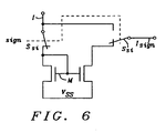
- Fig. 6 illustrates how to consider the sign bit of an incoming floating-point number.
- the output current I SIGN is either sunk or sourced.
- Current I is the output current of the linear IDAC as shown in Fig. 3 .
- Both switches S SI are controlled in parallel by the sign bit of the incoming floating point number.
- Dependent upon the position of the switches S SI the direction of the output current I SIGN remains unchanged compared to current I or the current I is directed through current mirror M and the output current I SIGN has a opposite direction compared to current I .
- One key advantage of the present invention is that the floating point number is directly converted into an analog current and no digital floating-point to integer conversion is necessary.
- the solution invented requires less chip area than a high resolution DAC, required in prior art.
Landscapes
- Physics & Mathematics (AREA)
- Nonlinear Science (AREA)
- Engineering & Computer Science (AREA)
- Theoretical Computer Science (AREA)
- Analogue/Digital Conversion (AREA)
Claims (25)
- Une méthode pour convertir directement un nombre numérique à virgule flottante en un signal analogique comportant:- la fourniture (40) d' un convertisseur numérique-analogique à courant linéaire (32) en cascade avec un convertisseur numérique-analogique à courant exponentiel (31);- le partage (40) d' un nombre à virgule flottante en sa mantisse et exposant; caractérisé en ce qu'elle comporte en outre:- la conversion (42) dudit exposant en un courant représentatif d' un signal numérique de l' exposant au moyen dudit convertisseur numérique-analogique à courant exponentiel dans lequel les bits (e0-e-2) dudit exposant modifient la largeur des transistors de miroir de courant (N10, N20) au sein dudit convertisseur numérique-analogique à courant exponentiel, dans laquelle ladite modification de la largeur des transistors des miroirs de courant (N10, N20) est effectuée en activant ou en désactivant les transistors commutables (N11, N12, N21, N22) disposés en parallèle auxdits transistors de miroir de courant et ainsi amplifiant ou diminuant des courants analogiques ; et- la conversion (43) dudit nombre numérique à virgule flottante en un courant analogique en convertissant ladite mantisse par ledit convertisseur numérique-analogique à courant linéaire en utilisant le courant de sortie de l'étape précédente comme un courant de référence de polarisation.
- La méthode de la revendication 1 dans laquelle ledit signal analogique de l' exposant est un courant.
- La méthode de la revendication 1 dans laquelle le courant de sortie dudit convertisseur numérique-analogique à courant exponentiel correspond à l'équation:

- La méthode de la revendication 1 dans laquelle le courant de sortie I dudit convertisseur numérique-analogique à courant linéaire (32) correspond à l' équation:

dans laquelle
- La méthode de la revendication 1 dans laquelle: ledit nombre numérique à virgule flottante est converti en un courant analogique en convertissant ledit exposant au moyen dudit convertisseur numérique-analogique à courant exponentiel (31) en utilisant le courant de sortie du convertisseur numérique-analogique à courant linéaire, en convertissant ladite mantisse, en tant que courant de polarisation de référence dans lequel les bits dudit exposant (e0-e-2) modifient la largeur des transistors de miroir de courant (N10, N20) au sein dudit convertisseur numérique-analogique à courant exponentiel et ainsi amplifiant ou réduisant les courants analogiques.
- La méthode de la revendication 5 dans laquelle le courant de sortie dudit convertisseur numérique-analogique à courant linéaire (32) correspond à l'équation:,

- La méthode de la revendication 5 dans laquelle le courant de sortie I dudit convertisseur numérique-analogique à courant exponentiel correspond à l' équation:

dans laquelle
- La méthode de la revendication 1 dans laquelle les largeurs desdits transistors (N11, N12, N21, N22) disposés en parallèle auxdits transistors de miroir de courant suivent la forme 22 j - 1 liée à la largeur des transistors de miroir de courant, dans laquelle i est l'index du bit accordé du vecteur dudit exposant.
- La méthode de la revendication 1 dans laquelle les rapports desdits miroirs de courant suivent la forme 22 j , dans laquelle j est l'index du bit accordé du vecteur dudit exposant.
- La méthode de la revendication 1 dans laquelle la direction du courant de sortie indique le signe dudit nombre à virgule flottant.
- La méthode de la revendication 10 dans laquelle ledit changement de la direction du courant de sortie est fourni par un miroir de courant et des commutateurs commandés par ledit signe.
- Un circuit pour convertir des nombres numériques à virgule flottante en un signal de courant analogique comportant:un convertisseur numérique-analogique à courant exponentiel (31), ledit convertisseur numérique-analogique à courant exponentiel comportant des transistors de miroir de courant (N10, N20) et des transistors commutables (N11, N12, N21, N22) arrangés en parallèle auxdits transistors de miroir de courant;ledit convertisseur numérique-analogique à courant exponentiel ayant une entrée et une sortie, dans lequel l'entrée est un vecteur comportant les bits de l'exposant dudit nombre à virgule flottante et dans lequel les bits de l'exposant peuvent activer ou désactiver lesdits transistors commutables, modifiant ainsi la largeur des transistors de miroir de courant et amplifiant ou réduisant ainsi un courant analogique, qui est la sortie du convertisseur numérique-analogique à courant exponentiel et qui est corrélé avec la valeur exponentielle dudit exposant;- un convertisseur numérique-analogique à courant linéaire (32) ayant des entrées et une sortie, dans lequel les entrées comportent un vecteur comportant la mantisse dudit nombre à virgule flottante et ledit courant de sortie analogique dudit convertisseur numérique-analogique à courant exponentiel et la sortie comporte un courant analogique étant corrélé de manière linéaire à la valeur dudit nombre numérique à virgule flottante; et- un moyen (M, Ssi) pour convertir la direction du courant de sortie en fonction du signe dudit nombre à virgule flottante.
- Le circuit de la revendication 12 dans lequel le courant de sortie dudit convertisseur numérique-analogique à courant exponentiel (31) correspond à l'équation:

- Le circuit de la revendication 12 dans lequel le courant de sortie I dudit convertisseur numérique-analogique à courant linéaire (32) correspond à l'équation:

dans laquelle
- Le circuit de la revendication 12 dans lequel lesdits moyens de conversion de la direction du courant de sortie comporte un moyens pour mettre en miroir (M) ledit courant de sortie et un arrangement de commutateurs (Ssi) activant le signe dudit nombre à point flottant.
- Le circuit de la revendication 12 dans lequel lesdits moyens pour convertir la direction dudit courant de sortie comportent :- un premier commutateur (Ssi), commandé par ledit bit de signe, dans lequel une première électrode dudit commutateur est connectée à la sortie dudit convertisseur linéaire et une deuxième électrode est connectée à un transistor d'entrée d'un miroir de courant;- ledit transistor d'entrée dudit miroir de courant (M) dans lequel le drain dudit transistor d'entrée est connecté à la deuxième électrode dudit premier commutateur et à sa grille, sa source étant connectée à la tension de VSS et sa grille étant connectée à la grille d'un transistor de sortie dudit miroir de courant;- ledit transistor de sortie dudit miroir de courant (M) dans lequel le drain dudit transistor de sortie est connecté à une deuxième électrode d'un deuxième commutateur et sa source est connectée à la tension de VSS ; et- ledit deuxième commutateur (Ssi), commandé par ledit signe de bit, commutant entre une première électrode est connectée à ladite sortie dudit convertisseur linéaire et ladite deuxième électrode, dans laquelle son point médian génère un courant de sortie d'une direction commandée par ledit signe de bit.
- Le circuit de la revendication 12 dans lequel- l'entrée dudit convertisseur numérique-analogique à courant linéaire (32) comporte un vecteur comportant les bits de la mantisse dudit nombre à virgule flottante et la sortie est un courant analogique qui est corrélé à la valeur linéaire de ladite mantisse et dans lequel les entrées dudit convertisseur numérique-analogique à courant exponentiel (32) comportent un vecteur comportant l'exposant dudit nombre à virgule flottante et ledit courant analogique de sortie dudit convertisseur numérique-analogique à courant linéaire et la sortie comporte un courant analogique étant linéairement corrélé à la valeur dudit nombre numérique à virgule flottante.
- Le circuit de la revendication 17 dans lequel le courant de sortie I dudit convertisseur numérique-analogique à courant exponentiel correspond à l'équation:

dans laquelle
- Le circuit de la revendication 12 dans lequel ledit convertisseur numérique-analogique à courant exponentiel, est capable de convertir n bits d'un exposant d'un nombre numérique à virgule flottante entrant comporte:- une source de courant (51), générant un courant de polarisation et ayant deux électrodes, dans laquelle une première électrode est connectée à la tension VDD et à une deuxième électrode au drain d'un premier commutateur de transistor NMOS (N12), au drain et à la grille d'un transistor d'entrée NMOS (N10) d'un premier miroir de courant, à la grille d'un transistor de sortie NMOS (N20) dudit premier miroir de courant, à la grille d'un deuxième transistor de NMOS (N11) étant parallèle audit transistor d'entrée (N10) dudit premier miroir de courant, et à la grille d'un troisième transistor de NMOS (N21) qui est parallèle audit transistor de sortie dudit premier miroir de courant;- un nombre d'étages, dans lequel ledit nombre d'étages est corrélé au nombre de bits dudit exposant et chaque étage est tour à tour déployé utilisant les technologies NMOS et PMOS et chaque étage comporte un miroir de courant (par exemple N10-N20, ou P10-P20), deux transistors (N11/N21, ou P11/P21), dans lequel chacun est disposé en parallèle au transistor d'entrée ou de sortie dudit miroir de courant, les deux commutateurs de transistor (N12/N22) ou (P12/P22), dans lesquels un desdits commutateurs de transistor est connecté à un desdits transistors disposés en parallèle à un desdits transistors d'entrée ou de sortie, dans lesquels chacun desdits commutateurs de transistor a sa grille connectée à un bit spécifique dudit exposant, et activant, en fonction de l'état dudit bit relatif dudit exposant, le transistor correspondant disposé en parallèle au transistor d'entrée, dans lequel la grille d'un premier commutateur de transistor d'un premier miroir de courant est connectée au bit de poids faible dudit exposant et chaque commutateur de transistor qui suit a sa grille connectée au prochain bit de l'exposant de droite vers la gauche, dans lequel les sources des miroirs de courant NMOS et des transistors parallèles relatifs sont connectées à la tension VSS avec leurs grilles sont toutes interconnectées, dans lequel les sources des miroirs de courant de PMOS et leurs transistors parallèles relatifs sont connectées à la tension de VDD avec leurs grilles sont interconnectées, dans lequel le courant de sortie d'un miroir de courant est le courant d'entrée du miroir de courant de l'étage qui suit à l'exception du dernier étage, dans laquelle son courant de sortie est la sortie du convertisseur numérique-analogique exponentiel.
- Le circuit de la revendication 19 dans lequel ledit nombre des étages est définie par l'équation

- Le circuit de la revendication 19 dans lequel les largeurs desdits transistors disposés en parallèle auxdits transistors de miroir de courant (N10/N20 ou P10/P20) faut suivre la forme 22 j - 1 liée à la largeur des transistors de miroir de courant, dans laquelle i est l'index du bit accordé du vecteur dudit exposant.
- Le circuit de la revendication 19 dans lequel lesdits rapports desdits miroirs de courant faut suivent la forme 22 j , dans laquelle j est l'index du bit accordé du vecteur dudit exposant.
- Le circuit de la revendication 19 dans lequel en cas d' un nombre impair de bits de l'exposant sont omis l'un des premiers commutateurs à transistor et l'un des premiers transistors disposés en parallèle à l'un desdits transistors d'entrée ou de sortie.
- Le circuit de la revendication 19 dans lequel en cas d' un nombre impair de bits de l'exposant sont omis l'un des second commutateurs à transistor et l'un des seconds transistors disposés en parallèle à l'un desdits transistors d'entrée ou de sortie sont omis.
- La méthode de la revendication 1 dans laquelle ledit convertisseur numérique-analogique à courant linéaire (32) est un convertisseur numérique-analogique à courant linéaire à basse résolution.
Priority Applications (3)
| Application Number | Priority Date | Filing Date | Title |
|---|---|---|---|
| AT04392040T ATE511243T1 (de) | 2004-11-12 | 2004-11-12 | Gleitkomma idac |
| EP04392040A EP1657823B1 (fr) | 2004-11-12 | 2004-11-12 | IDAC à virgule flottante |
| US10/990,004 US7132966B2 (en) | 2004-11-12 | 2004-11-16 | Floating point IDAC |
Applications Claiming Priority (1)
| Application Number | Priority Date | Filing Date | Title |
|---|---|---|---|
| EP04392040A EP1657823B1 (fr) | 2004-11-12 | 2004-11-12 | IDAC à virgule flottante |
Publications (2)
| Publication Number | Publication Date |
|---|---|
| EP1657823A1 EP1657823A1 (fr) | 2006-05-17 |
| EP1657823B1 true EP1657823B1 (fr) | 2011-05-25 |
Family
ID=34931996
Family Applications (1)
| Application Number | Title | Priority Date | Filing Date |
|---|---|---|---|
| EP04392040A Expired - Lifetime EP1657823B1 (fr) | 2004-11-12 | 2004-11-12 | IDAC à virgule flottante |
Country Status (3)
| Country | Link |
|---|---|
| US (1) | US7132966B2 (fr) |
| EP (1) | EP1657823B1 (fr) |
| AT (1) | ATE511243T1 (fr) |
Families Citing this family (4)
| Publication number | Priority date | Publication date | Assignee | Title |
|---|---|---|---|---|
| EP2894943B1 (fr) * | 2014-01-14 | 2020-02-26 | Dialog Semiconductor (UK) Limited | Appareil permettant d'améliorer la précision d'un convertisseur numérique-analogique (IDAC) exponentiel utilisant un MSB à pondération binaire |
| EP2894944A1 (fr) * | 2014-01-14 | 2015-07-15 | Dialog Semiconductor GmbH | Procédé permettant d'améliorer la précision d'un convertisseur numérique-analogique (IDAC) exponentiel utilisant un MSB à pondération binaire |
| CN118381911A (zh) * | 2018-03-21 | 2024-07-23 | Lx 半导体科技有限公司 | 图像编码/解码方法以及图像数据的发送方法 |
| CN112636761B (zh) * | 2020-12-09 | 2024-04-12 | 二十一世纪(北京)微电子技术有限公司 | 一种指数基准电流型的数字模拟转换电路及电子设备 |
Family Cites Families (19)
| Publication number | Priority date | Publication date | Assignee | Title |
|---|---|---|---|---|
| US4278964A (en) * | 1971-06-14 | 1981-07-14 | Texaco Inc. | Seismic playback system |
| US3673398A (en) * | 1971-06-30 | 1972-06-27 | Texaco Inc | Seismic playback system |
| DE2430018C3 (de) * | 1974-06-22 | 1980-03-13 | Deutsche Texaco Ag, 2000 Hamburg | Anordnung zur stufenlosen Kompression digital gespeicherter Datenfolgen zwecks analoger Wiedergabe |
| US4594577A (en) * | 1980-09-02 | 1986-06-10 | American Microsystems, Inc. | Current mirror digital to analog converter |
| US4393369A (en) * | 1981-03-16 | 1983-07-12 | The United States Of America As Represented By The Secretary Of The Navy | Floating-point A/D and D/A converter |
| JPS5995595A (ja) * | 1982-11-25 | 1984-06-01 | ヤマハ株式会社 | 電子楽器 |
| JPS6060694A (ja) * | 1983-09-14 | 1985-04-08 | ヤマハ株式会社 | 波形発生装置 |
| JPH0712150B2 (ja) * | 1985-04-19 | 1995-02-08 | ヤマハ株式会社 | ディジタル・アナログ変換器 |
| WO1988008574A1 (fr) * | 1987-04-28 | 1988-11-03 | Fujitsu Ten Limited | Procede et appareil pour le transfert de donnees |
| JPS63299516A (ja) * | 1987-05-29 | 1988-12-07 | Alpine Electron Inc | デジタル・アナログ変換器 |
| US5323159A (en) * | 1990-04-20 | 1994-06-21 | Nakamichi Corporation | Digital/analog converter |
| US5053770A (en) * | 1990-05-18 | 1991-10-01 | Analogic Corporation | Digital autozero circuit operable in a plurality of modes with separate storage for offset corrections for each mode |
| US5061927A (en) * | 1990-07-31 | 1991-10-29 | Q-Dot, Inc. | Floating point analog to digital converter |
| US5404143A (en) * | 1991-06-12 | 1995-04-04 | Intellectual Property Development Associates Of Connecticut, Inc. | Network swappers and circuits constructed from same |
| US5764548A (en) * | 1995-09-29 | 1998-06-09 | Intel Corporation | Fast floating-point to integer conversion |
| US6388388B1 (en) * | 2000-12-27 | 2002-05-14 | Visteon Global Technologies, Inc. | Brightness control system and method for a backlight display device using backlight efficiency |
| US6850177B2 (en) * | 2001-05-14 | 2005-02-01 | Xyron Corporation | Digital to analog convertor |
| US7028067B2 (en) * | 2002-02-20 | 2006-04-11 | International Business Machines Corporation | Generation of mask-constrained floating-point addition and subtraction test cases, and method and system therefor |
| US6999098B2 (en) * | 2002-11-27 | 2006-02-14 | Ati Technologies Inc. | Apparatus for converting floating point values to gamma corrected fixed point values |
-
2004
- 2004-11-12 EP EP04392040A patent/EP1657823B1/fr not_active Expired - Lifetime
- 2004-11-12 AT AT04392040T patent/ATE511243T1/de not_active IP Right Cessation
- 2004-11-16 US US10/990,004 patent/US7132966B2/en not_active Expired - Lifetime
Also Published As
| Publication number | Publication date |
|---|---|
| EP1657823A1 (fr) | 2006-05-17 |
| US20060103562A1 (en) | 2006-05-18 |
| ATE511243T1 (de) | 2011-06-15 |
| US7132966B2 (en) | 2006-11-07 |
Similar Documents
| Publication | Publication Date | Title |
|---|---|---|
| US5489904A (en) | Analog current mode analog/digital converter | |
| US4594577A (en) | Current mirror digital to analog converter | |
| US5283579A (en) | Digital to analog converter having high multiplying bandwidth | |
| KR20100031615A (ko) | 코드 의존 dc 전류를 이용하는 의사-차동 클래스-ab 디지털-아날로그 변환기 | |
| GB2393055A (en) | A transconductance amplifier with input sampling capacitor for a current-interpolating A-D converter | |
| US7030799B2 (en) | Current-steering digital-to-analog converter | |
| US6995700B2 (en) | High-resolution digital-to-analog converter | |
| EP1657823B1 (fr) | IDAC à virgule flottante | |
| JP3099717B2 (ja) | D/a変換回路 | |
| US20060181343A1 (en) | Gain controlled amplifier and cascoded gain controlled amplifier based on the same | |
| CN113839674B (zh) | 一种模数转换电路 | |
| US5296857A (en) | Digital to analog converter with precise linear output for both positive and negative digital input values | |
| EP0200970B1 (fr) | Convertisseur numérique-analogique | |
| US5021785A (en) | Floating point digital to analog converter with bias to establish range midpoint | |
| US5220306A (en) | Digital signal comparator for comparing n-bit binary signals | |
| WO1981000653A1 (fr) | Systeme de conversion cyclique digital/analogique | |
| US6509856B2 (en) | Digital-to-analog converter | |
| EP1107459A2 (fr) | Méthode et appareil pour éliminer de façon numérique un décalage continu plus petit qu'un LSB | |
| CN110022110B (zh) | 音圈马达阻尼控制电路 | |
| CN115296671A (zh) | 混合结构的数模转换电路 | |
| US7986258B2 (en) | Analog-digital conversion cell and analog-digital converter | |
| EP0177902B1 (fr) | Convertisseur numérique-analogique | |
| JPS61295722A (ja) | D/a変換器のゲイン調整方式 | |
| KR20020092000A (ko) | 범용 4사분면 아날로그-디지털 곱셈기 | |
| CN120658263A (zh) | 数模转换电路及控制芯片 |
Legal Events
| Date | Code | Title | Description |
|---|---|---|---|
| PUAI | Public reference made under article 153(3) epc to a published international application that has entered the european phase |
Free format text: ORIGINAL CODE: 0009012 |
|
| AK | Designated contracting states |
Kind code of ref document: A1 Designated state(s): AT BE BG CH CY CZ DE DK EE ES FI FR GB GR HU IE IS IT LI LU MC NL PL PT RO SE SI SK TR |
|
| AX | Request for extension of the european patent |
Extension state: AL HR LT LV MK YU |
|
| 17P | Request for examination filed |
Effective date: 20061117 |
|
| AKX | Designation fees paid |
Designated state(s): AT BE BG CH CY CZ DE DK EE ES FI FR GB GR HU IE IS IT LI LU MC NL PL PT RO SE SI SK TR |
|
| 17Q | First examination report despatched |
Effective date: 20070315 |
|
| GRAP | Despatch of communication of intention to grant a patent |
Free format text: ORIGINAL CODE: EPIDOSNIGR1 |
|
| GRAS | Grant fee paid |
Free format text: ORIGINAL CODE: EPIDOSNIGR3 |
|
| GRAA | (expected) grant |
Free format text: ORIGINAL CODE: 0009210 |
|
| AK | Designated contracting states |
Kind code of ref document: B1 Designated state(s): AT BE BG CH CY CZ DE DK EE ES FI FR GB GR HU IE IS IT LI LU MC NL PL PT RO SE SI SK TR |
|
| REG | Reference to a national code |
Ref country code: GB Ref legal event code: FG4D |
|
| REG | Reference to a national code |
Ref country code: CH Ref legal event code: EP |
|
| REG | Reference to a national code |
Ref country code: IE Ref legal event code: FG4D |
|
| REG | Reference to a national code |
Ref country code: DE Ref legal event code: R096 Ref document number: 602004032839 Country of ref document: DE Effective date: 20110707 |
|
| REG | Reference to a national code |
Ref country code: NL Ref legal event code: VDEP Effective date: 20110525 |
|
| PG25 | Lapsed in a contracting state [announced via postgrant information from national office to epo] |
Ref country code: SE Free format text: LAPSE BECAUSE OF FAILURE TO SUBMIT A TRANSLATION OF THE DESCRIPTION OR TO PAY THE FEE WITHIN THE PRESCRIBED TIME-LIMIT Effective date: 20110525 Ref country code: PT Free format text: LAPSE BECAUSE OF FAILURE TO SUBMIT A TRANSLATION OF THE DESCRIPTION OR TO PAY THE FEE WITHIN THE PRESCRIBED TIME-LIMIT Effective date: 20110926 |
|
| PG25 | Lapsed in a contracting state [announced via postgrant information from national office to epo] |
Ref country code: GR Free format text: LAPSE BECAUSE OF FAILURE TO SUBMIT A TRANSLATION OF THE DESCRIPTION OR TO PAY THE FEE WITHIN THE PRESCRIBED TIME-LIMIT Effective date: 20110826 Ref country code: AT Free format text: LAPSE BECAUSE OF FAILURE TO SUBMIT A TRANSLATION OF THE DESCRIPTION OR TO PAY THE FEE WITHIN THE PRESCRIBED TIME-LIMIT Effective date: 20110525 Ref country code: ES Free format text: LAPSE BECAUSE OF FAILURE TO SUBMIT A TRANSLATION OF THE DESCRIPTION OR TO PAY THE FEE WITHIN THE PRESCRIBED TIME-LIMIT Effective date: 20110905 Ref country code: IS Free format text: LAPSE BECAUSE OF FAILURE TO SUBMIT A TRANSLATION OF THE DESCRIPTION OR TO PAY THE FEE WITHIN THE PRESCRIBED TIME-LIMIT Effective date: 20110925 Ref country code: FI Free format text: LAPSE BECAUSE OF FAILURE TO SUBMIT A TRANSLATION OF THE DESCRIPTION OR TO PAY THE FEE WITHIN THE PRESCRIBED TIME-LIMIT Effective date: 20110525 Ref country code: SI Free format text: LAPSE BECAUSE OF FAILURE TO SUBMIT A TRANSLATION OF THE DESCRIPTION OR TO PAY THE FEE WITHIN THE PRESCRIBED TIME-LIMIT Effective date: 20110525 Ref country code: CY Free format text: LAPSE BECAUSE OF FAILURE TO SUBMIT A TRANSLATION OF THE DESCRIPTION OR TO PAY THE FEE WITHIN THE PRESCRIBED TIME-LIMIT Effective date: 20110525 Ref country code: BE Free format text: LAPSE BECAUSE OF FAILURE TO SUBMIT A TRANSLATION OF THE DESCRIPTION OR TO PAY THE FEE WITHIN THE PRESCRIBED TIME-LIMIT Effective date: 20110525 |
|
| PG25 | Lapsed in a contracting state [announced via postgrant information from national office to epo] |
Ref country code: NL Free format text: LAPSE BECAUSE OF FAILURE TO SUBMIT A TRANSLATION OF THE DESCRIPTION OR TO PAY THE FEE WITHIN THE PRESCRIBED TIME-LIMIT Effective date: 20110525 |
|
| PG25 | Lapsed in a contracting state [announced via postgrant information from national office to epo] |
Ref country code: CZ Free format text: LAPSE BECAUSE OF FAILURE TO SUBMIT A TRANSLATION OF THE DESCRIPTION OR TO PAY THE FEE WITHIN THE PRESCRIBED TIME-LIMIT Effective date: 20110525 Ref country code: EE Free format text: LAPSE BECAUSE OF FAILURE TO SUBMIT A TRANSLATION OF THE DESCRIPTION OR TO PAY THE FEE WITHIN THE PRESCRIBED TIME-LIMIT Effective date: 20110525 |
|
| PG25 | Lapsed in a contracting state [announced via postgrant information from national office to epo] |
Ref country code: PL Free format text: LAPSE BECAUSE OF FAILURE TO SUBMIT A TRANSLATION OF THE DESCRIPTION OR TO PAY THE FEE WITHIN THE PRESCRIBED TIME-LIMIT Effective date: 20110525 Ref country code: SK Free format text: LAPSE BECAUSE OF FAILURE TO SUBMIT A TRANSLATION OF THE DESCRIPTION OR TO PAY THE FEE WITHIN THE PRESCRIBED TIME-LIMIT Effective date: 20110525 Ref country code: RO Free format text: LAPSE BECAUSE OF FAILURE TO SUBMIT A TRANSLATION OF THE DESCRIPTION OR TO PAY THE FEE WITHIN THE PRESCRIBED TIME-LIMIT Effective date: 20110525 Ref country code: DK Free format text: LAPSE BECAUSE OF FAILURE TO SUBMIT A TRANSLATION OF THE DESCRIPTION OR TO PAY THE FEE WITHIN THE PRESCRIBED TIME-LIMIT Effective date: 20110525 |
|
| PLBE | No opposition filed within time limit |
Free format text: ORIGINAL CODE: 0009261 |
|
| STAA | Information on the status of an ep patent application or granted ep patent |
Free format text: STATUS: NO OPPOSITION FILED WITHIN TIME LIMIT |
|
| 26N | No opposition filed |
Effective date: 20120228 |
|
| PG25 | Lapsed in a contracting state [announced via postgrant information from national office to epo] |
Ref country code: IT Free format text: LAPSE BECAUSE OF FAILURE TO SUBMIT A TRANSLATION OF THE DESCRIPTION OR TO PAY THE FEE WITHIN THE PRESCRIBED TIME-LIMIT Effective date: 20110525 |
|
| REG | Reference to a national code |
Ref country code: DE Ref legal event code: R097 Ref document number: 602004032839 Country of ref document: DE Effective date: 20120228 |
|
| PG25 | Lapsed in a contracting state [announced via postgrant information from national office to epo] |
Ref country code: MC Free format text: LAPSE BECAUSE OF NON-PAYMENT OF DUE FEES Effective date: 20111130 |
|
| REG | Reference to a national code |
Ref country code: CH Ref legal event code: PL |
|
| PG25 | Lapsed in a contracting state [announced via postgrant information from national office to epo] |
Ref country code: CH Free format text: LAPSE BECAUSE OF NON-PAYMENT OF DUE FEES Effective date: 20111130 Ref country code: LI Free format text: LAPSE BECAUSE OF NON-PAYMENT OF DUE FEES Effective date: 20111130 |
|
| REG | Reference to a national code |
Ref country code: IE Ref legal event code: MM4A |
|
| PG25 | Lapsed in a contracting state [announced via postgrant information from national office to epo] |
Ref country code: IE Free format text: LAPSE BECAUSE OF NON-PAYMENT OF DUE FEES Effective date: 20111112 |
|
| PGFP | Annual fee paid to national office [announced via postgrant information from national office to epo] |
Ref country code: FR Payment date: 20130329 Year of fee payment: 9 |
|
| PG25 | Lapsed in a contracting state [announced via postgrant information from national office to epo] |
Ref country code: LU Free format text: LAPSE BECAUSE OF NON-PAYMENT OF DUE FEES Effective date: 20111112 |
|
| PG25 | Lapsed in a contracting state [announced via postgrant information from national office to epo] |
Ref country code: BG Free format text: LAPSE BECAUSE OF FAILURE TO SUBMIT A TRANSLATION OF THE DESCRIPTION OR TO PAY THE FEE WITHIN THE PRESCRIBED TIME-LIMIT Effective date: 20110825 |
|
| PG25 | Lapsed in a contracting state [announced via postgrant information from national office to epo] |
Ref country code: TR Free format text: LAPSE BECAUSE OF FAILURE TO SUBMIT A TRANSLATION OF THE DESCRIPTION OR TO PAY THE FEE WITHIN THE PRESCRIBED TIME-LIMIT Effective date: 20110525 |
|
| PG25 | Lapsed in a contracting state [announced via postgrant information from national office to epo] |
Ref country code: HU Free format text: LAPSE BECAUSE OF FAILURE TO SUBMIT A TRANSLATION OF THE DESCRIPTION OR TO PAY THE FEE WITHIN THE PRESCRIBED TIME-LIMIT Effective date: 20110525 |
|
| REG | Reference to a national code |
Ref country code: FR Ref legal event code: ST Effective date: 20140731 |
|
| PG25 | Lapsed in a contracting state [announced via postgrant information from national office to epo] |
Ref country code: FR Free format text: LAPSE BECAUSE OF NON-PAYMENT OF DUE FEES Effective date: 20131202 |
|
| PGFP | Annual fee paid to national office [announced via postgrant information from national office to epo] |
Ref country code: DE Payment date: 20151106 Year of fee payment: 12 Ref country code: GB Payment date: 20151105 Year of fee payment: 12 |
|
| REG | Reference to a national code |
Ref country code: DE Ref legal event code: R119 Ref document number: 602004032839 Country of ref document: DE |
|
| GBPC | Gb: european patent ceased through non-payment of renewal fee |
Effective date: 20161112 |
|
| PG25 | Lapsed in a contracting state [announced via postgrant information from national office to epo] |
Ref country code: DE Free format text: LAPSE BECAUSE OF NON-PAYMENT OF DUE FEES Effective date: 20170601 Ref country code: GB Free format text: LAPSE BECAUSE OF NON-PAYMENT OF DUE FEES Effective date: 20161112 |