EP1665779B1 - Systeme de capture d'images et son utilisation - Google Patents
Systeme de capture d'images et son utilisation Download PDFInfo
- Publication number
- EP1665779B1 EP1665779B1 EP05706929A EP05706929A EP1665779B1 EP 1665779 B1 EP1665779 B1 EP 1665779B1 EP 05706929 A EP05706929 A EP 05706929A EP 05706929 A EP05706929 A EP 05706929A EP 1665779 B1 EP1665779 B1 EP 1665779B1
- Authority
- EP
- European Patent Office
- Prior art keywords
- recognition system
- image recognition
- image
- optical
- array
- Prior art date
- Legal status (The legal status is an assumption and is not a legal conclusion. Google has not performed a legal analysis and makes no representation as to the accuracy of the status listed.)
- Expired - Lifetime
Links
Images


Classifications
-
- G—PHYSICS
- G02—OPTICS
- G02B—OPTICAL ELEMENTS, SYSTEMS OR APPARATUS
- G02B3/00—Simple or compound lenses
- G02B3/0006—Arrays
- G02B3/0012—Arrays characterised by the manufacturing method
-
- H—ELECTRICITY
- H04—ELECTRIC COMMUNICATION TECHNIQUE
- H04N—PICTORIAL COMMUNICATION, e.g. TELEVISION
- H04N25/00—Circuitry of solid-state image sensors [SSIS]; Control thereof
-
- G—PHYSICS
- G02—OPTICS
- G02B—OPTICAL ELEMENTS, SYSTEMS OR APPARATUS
- G02B13/00—Optical objectives specially designed for the purposes specified below
- G02B13/001—Miniaturised objectives for electronic devices, e.g. portable telephones, webcams, PDAs, small digital cameras
- G02B13/0055—Miniaturised objectives for electronic devices, e.g. portable telephones, webcams, PDAs, small digital cameras employing a special optical element
-
- G—PHYSICS
- G02—OPTICS
- G02B—OPTICAL ELEMENTS, SYSTEMS OR APPARATUS
- G02B3/00—Simple or compound lenses
- G02B3/0006—Arrays
- G02B3/0037—Arrays characterized by the distribution or form of lenses
- G02B3/0043—Inhomogeneous or irregular arrays, e.g. varying shape, size, height
-
- G—PHYSICS
- G02—OPTICS
- G02B—OPTICAL ELEMENTS, SYSTEMS OR APPARATUS
- G02B3/00—Simple or compound lenses
- G02B3/0006—Arrays
- G02B3/0037—Arrays characterized by the distribution or form of lenses
- G02B3/0056—Arrays characterized by the distribution or form of lenses arranged along two different directions in a plane, e.g. honeycomb arrangement of lenses
-
- G—PHYSICS
- G02—OPTICS
- G02B—OPTICAL ELEMENTS, SYSTEMS OR APPARATUS
- G02B3/00—Simple or compound lenses
- G02B3/0006—Arrays
- G02B3/0075—Arrays characterized by non-optical structures, e.g. having integrated holding or alignment means
-
- G—PHYSICS
- G06—COMPUTING OR CALCULATING; COUNTING
- G06V—IMAGE OR VIDEO RECOGNITION OR UNDERSTANDING
- G06V40/00—Recognition of biometric, human-related or animal-related patterns in image or video data
- G06V40/10—Human or animal bodies, e.g. vehicle occupants or pedestrians; Body parts, e.g. hands
- G06V40/12—Fingerprints or palmprints
- G06V40/13—Sensors therefor
- G06V40/1324—Sensors therefor by using geometrical optics, e.g. using prisms
-
- H—ELECTRICITY
- H04—ELECTRIC COMMUNICATION TECHNIQUE
- H04N—PICTORIAL COMMUNICATION, e.g. TELEVISION
- H04N23/00—Cameras or camera modules comprising electronic image sensors; Control thereof
- H04N23/50—Constructional details
- H04N23/55—Optical parts specially adapted for electronic image sensors; Mounting thereof
Definitions
- the invention relates to a digital image acquisition system with a minimum length of less than 1 mm.
- the image acquisition system here consists of a microlens array, a detector array and optionally a pinhole array.
- the operation of this image acquisition system is based on a separate mapping of different solid angle segments of the object space by a plurality of parallel optical channels.
- a single optical channel maps all information from the object space into the image plane.
- the objective forms the entire detectable angular range of the object space.
- the field of view of the arrangement is limited by the maximum possible pitch difference between lens and pinhole array.
- An arrangement of a plurality of said modules on a curved base surface for scaling the field of view and the number of channels is proposed. However, this completely contradicts a desired system integration.
- An additionally arranged in front of the lens array diverging lens generates an enlargement of the angular field of view, which means a smaller image and thus allows an increase in the object distance while maintaining the function of the system.
- the used pinhole diameters are 140 ⁇ m, which does not allow a good resolution of the system.
- the image acquisition takes place centrally behind the microlenses.
- Metal partitions and crossed polarizing filters are used for optical isolation to minimize crosstalk.
- individually manufactured components are also elaborately adjusted to each other, which leads to the emergence of additional sources of error and costs.
- a Provisional array with variable deflection angles, a diverging lens or the integration of a beam deflection proposed in diffractive lenses This would not increase the system thickness.
- a concrete resolution of the system was not specified.
- decentered microlenses is thus seen as a substitute for a large imaging lens, but without an effect on the length of the optics, as long as a significant reduction of the individual images and thus loss of effective magnification or loss of resolution is accepted.
- a possible pitch difference between microlens array and detector subgroups to produce effective magnification is not indicated.
- the effective (negative) enlargement of the overall system is therefore not increased by the cited invention. Given possible system lengths are therefore always much larger than 1 mm. There is no reference to the possibility of assigning a microlens only one detector pixel at a time.
- Space filling arrays are used to increase the fill factor.
- Classic lenses are used to image the object, which significantly increases the system length and limits the use of these promising sensors in everyday life (eg in the automotive sector).
- Linking the present invention to the aforementioned sensors as an exchange for the focal plane array and macroscopic imaging optics meant extreme added value generation due to significant system shortening and integration.
- JP 2001-210812 A From the JP 2001-210812 A is an optical system with a plurality of optical channels with respective microlens and shown arranged in the focal plane detector.
- This optical system is behind a conventional realizing the actual image Optics arranged.
- the detector pixels are approximately the same size as the microlenses, whereby a very large angular range of the object can be imaged on a single pixel. This results in an imaging system with only low resolution.
- an object of the present invention to provide an image acquisition system having improved mechanical and optical parameters such as system length, field of view, resolution, image size and luminous intensity.
- an image acquisition system consisting of regularly arranged optical channels with a microlens and at least one detector lying in its focal line, which from the microimage behind the Microlens at least one pixel extracted, provided.
- the optical axes of the individual optical channels have different inclinations, so that they represent a function of the distance of the optical channel from the center of the image facing side of the image acquisition system and thus the ratio of the size of the field of view of the optics to image field size can be determined.
- detectors are used with such high sensitivity that they have a large pitch with a small active area.
- the described flat camera consists of a microlens array and a detector array lying in its focal plane or an optional pinhole array which covers a detector array of active areas larger than those of the pixels.
- pixel is understood to be an area with the desired spectral sensitivity.
- a microimage of the object is formed, which is statically scanned by the detector or pinhole array.
- Each microlens is one or a few photosensitive pixels, e.g. with different functions, e.g. spectral sensitivities, assigned.
- the offset of the photosensitive pixel within the microimage from cell to cell generated in various ways, scans and captures the entire image over the entire array.
- the tilt of the optical axis of an optical channel consisting of a microlens and a pinhole extracting a pixel from the microimage behind this lens is a function of its radial coordinate in the array.
- the imaging principle of the invention can be independent from the spectral range and is therefore generally usable from UV via VIS up to the deep IR, with appropriate adaptation of the materials to be used for optics and receiver to the spectral range.
- the use for IR sensors seems particularly attractive since here the microlens arrays can be made, for example, in silicon or germanium (or limited also corresponding polymers), which has the advantage that no large and thus extremely expensive germanium or silicon lenses are needed, but only very thin microlens arrays, resulting in significant material and mass savings and thus cost savings.
- IR sensors often have a large pitch with small active pixel area and therefore require fill factor increasing lens arrays.
- the combination of conventional imaging optics with filling factor increasing lens array can be replaced by the invention by only one imaging lens array.
- temperature fields determining bolometer arrays can be provided with ultra-flat imaging systems.
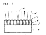
- the adjacent cells are optically isolated (cf. Fig. 2 ).
- the inclined optical axes By virtue of the inclined optical axes to be ensured in various ways, they observe the object space separately from or only with minimal angular overlap to the adjacent imaging units.
- Each optical channel therefore provides at least one image pixel (possibly in different colors) corresponding to a solid angle region in the object space within the field of view of the entire optics.
- the combination of all the signals supplied by the individual optical channels allows the reconstruction the object distribution.
- Said arrangement can be advantageously combined, especially with photo-electronic sensors, which have a high sensitivity or contrast sensitivity, but have a relatively large pitch at small pixels (low fill factor).
- the described arrangement is produced with modern micro-optical technologies on system and wafer scale. Complex assembly and adjustment steps of individually manufactured components are eliminated. The greatest possible system integration, precision and price attractiveness is the result.
- the number of optical channels can be adapted to the application and vary in the range of reasonable 10x10 to 1000x1000 channels (for high-resolution images).
- the lateral extent of the camera chip under 1x1 mm 2 can be more than 10x10 mm 2 .
- Non-square arrangements are also conceivable in order to adapt to detector geometry or to the shape of the visual field.
- Non-round lenses (anamorphic lenses) to correct the off-axis aberrations are conceivable.
- a combination of the image-receiving channels with light sources (eg OLEDs) lying therebetween or lying on them is very advantageous for a further reduction of the overall length or the required volume of an imaging arrangement, since illumination is not required from the side or in up or down as usual Transmitted light must be supplied. This opens up even the smallest and narrowest workspaces, eg in microsystem technology or endoscopy in medicine.
- light sources eg OLEDs
- a variant according to the invention provides that a correction of off-axis image defects by use of different anamorphic lenses, in particular elliptical enamel lenses, for each individual channel is made possible.
- the correction of the astigmatism and field curvature allows the image to remain equally sharp throughout the field of view as the shape of the lens of each channel is adjusted individually to the angle of incidence to be transmitted.
- the lens has two different major radii of curvature. The orientation of the ellipses is always such that the axis of a main radius of curvature in the direction of the increasing angle of incidence and that of the other main radius of curvature is perpendicular thereto.
- Both main radii of curvature increase with increasing angle of incidence according to analytically derivable laws, whereby the radii increase to different degrees.
- An adjustment of the principal curvature radius ratio of the lens of a single channel can be made by adjusting the axis ratio of the ellipse base.
- the adjustment of the radius of curvature change from channel to channel is achieved by adjusting the size of the axes.
- a correction of the distortion ie of the main beam error angle
- a correction of the distortion can be achieved by an adapted position of the pinhole or detector in the image of a microlens.
- a correction of the distortion is possible simply by a non-constant pitch difference between lens array and pinhole or detector array.
- the position of the respective microlens not only has to be offset by a multiple of the pitch difference with respect to the detector, but has to be adapted to the real main beam angle to be processed.
- the functions described here can also be achieved by the integration of the pixels of the individual channel different structures / elements in the plane of the microlenses.
- the channels differ in their optical functions and not only in their viewing directions.
- a coarser and simpler structuring of the electronics is the positive result.
- the disadvantage is the possibly necessary larger number of channels and the associated greater lateral space requirement for an equivalent resolution.
- a combination of several different pixels per channel with different optical properties of different channels can make sense be. Since the system described can be produced on a wafer scale, it is possible to increase the light intensity of the image by separating not individual cameras but entire groups (arrays of cameras) by simply recording several cameras in the same image (angle correction may be necessary) and these Images are then superimposed electronically.
- a significant improvement in the characteristics of the described invention can be achieved by an additional arrangement of the detectors on a curved base surface, as in FIG Fig. 7 represented reached.
- the radius of curvature of the spherical shell on which the detectors are located is just as much smaller to choose than that of the spherical shell on which the microlenses are located, that microlenses of the same focal length on the first spherical shell exactly on the receptors focus on the second spherical shell.
- the two spherical shells are concentric. The choice of this arrangement results in the imaging of a large field of view, without off-axis aberrations, since an optical channel is always axisymmetric for an object point to be imaged by it. Identical microlenses can be used.
- Naturally occurring imaging systems i. Eyes possess, as far as we know, curved retinas (natural receptor arrays) without exception. This applies to single-chamber eyes as well as to facetted eyes.
- the curvature of the retina achieves a significant reduction in the field-dependent aberrations (field curvature, astigmatism) and thus a more homogeneous resolution and more uniform illumination across the field of view.
- field curvature, astigmatism field curvature, astigmatism
- a very large field of view is made possible. Even with simple lens systems, well-resolved images of the environment can be generated.
- the simultaneous front and rear hot stamping / UV casting in a thin plate or foil which can be easily placed on the sensor array and glued, particularly advantageous.
- the lens arrays are embossed on the front and on the back of the crossed trenches, which are by subsequent filling with black or absorbent potting compound, the optically insulating walls of the channels.
- the molding tools of the lens arrays for hot stamping can be produced for example by galvanic molding of the prototypes, while transparent tools are necessary for the UV casting.
- Prototypes / tools of the optical structures whether similar lenses or lenses of varying parameters (“chirped lens arrays") can be used, for example, by the reflow process, gray toned lithography, laser writing, ultra-precision machining, laser ablation and combinations of these technologies can be generated and can also Lenses with integrated prisms or grids or from offset relative to the channel center lens segments exist.
- the prototypes / tools for the crossed walls for example, by lithography in very high aspect ratio patternable photoresist (SU8) or by ultra-precision machining, such as form-drilling of round or milling square or rectangular trench structures, the Bosch-silicon process (deep dry etching with a very high aspect ratio), wet etching of silicon in KOH (anisotropic), the LIGA process, or laser ablation.
- a generation of these walls by a planar exposure of a back-unstructured substrate with a high-power laser, so-called.
- Excimer laser through a lithographic mask with crossed bars and resulting blackening of the exposed areas is also conceivable, the black walls are produced with a bombardment.
- the same effect can be achieved by machining the material with a high power focused laser beam, with the crossed walls then forming tracks of a scanning deflection of the laser focus. Here the black walls are written in the material.
- Manufacturing of the masters / tools by ultra-precision machining machines may result in high surface roughness. This can e.g. be compensated or minimized by spray coating ("spray coating") with a thin polymer film of suitable refractive index (prisms, aspherical lens segments, (blazed) grids, crossed 1D array structures).
- spray coating with a thin polymer film of suitable refractive index (prisms, aspherical lens segments, (blazed) grids, crossed 1D array structures).
- a surface bonding of the ultra-flat optics with the sensor leads to a significant reduction of the Fresnel reflection losses, since two interfaces to air are eliminated.
- the shape of the black walls does not necessarily have to be such that the transparent volumes of the channels are cuboid, but may also result in transparent conical or pyramidal pitch structures between the lens array and the image plane.
- Replication technologies include W-curable polymer impression molding, double-sided embossing or printing on plastic film, plastic molding or injection molding, hot stamping of thin plastic sheets, and UV reaction casting directly onto optoelectronic wafers used.
- the use as an integral part in flat-building small appliances such as watches, notebooks, PDAs or organizers, mobile phones, eyewear, garments, for monitoring and security technology, as well as for the control and enforcement of access or use permissions conceivable.
- Another very attractive application is the use as a camera in a credit card or in the general case smart card.
- a camera as a sticker and as an ultra-flat imaging system for machine vision in the automotive sector as well as in medical technology is made possible by the arrangement according to the invention.
- the image-receiving pixels in the camera do not necessarily have to be densely packed, but can, for example, also alternate with slightly extended light sources, eg LEDs (also in color).
- slightly extended light sources eg LEDs (also in color).
- image-picking and sometimeswiederbiede pixels are uniform distributed in large arrays, for simultaneous image acquisition and image reproduction possible.
- the imaging system according to the invention can also be used in the field of endoscopy.
- a curved image sensor can be used e.g. be raised on a cylinder jacket. This allows a panoramic view in accessible to endoscopy organs.
- Another use relates to the detection of the sun's position or the determination of the relative position of a punctiform or only slightly extended light source to a reference surface fixedly connected to the flat camera. This requires a relatively high and possibly asymmetrical field of view, approximately 60 ° x 30 ° full angles.
- Another use relates to the recording and processing of so-called smart labels.
- a reconfigurable pattern recognition can be realized. This means that the gaze towards each channel can be switched electronically, resulting in a redistribution in the mapping of image and object information. This can be used, for example, to define other object patterns from time to time without having to replace the camera.
- the use relates to the recognition and identification of logos.
- Another field of application relates to microsystem technology, e.g. as a camera to observe the workspace.
- grippers on the jaws or arms may have corresponding image acquisition systems.
- This also includes the application in the field of "Machine Vision", e.g. compact cameras for pick and place robots with high magnification and at the same time high depth of field but also up to all-round visibility, e.g. for borehole inspections.
- a flat camera here has enormous advantages, since no high resolution but only high depth of field is needed.
- Another use relates to the 3D motion tracking, for example, the hand of a person or the whole person to implement in 3D virtual reality or for the monitoring technology.
- 3D motion tracking for example, the hand of a person or the whole person to implement in 3D virtual reality or for the monitoring technology.
- cost-effective large-area receiver arrays are needed, which is fulfilled by the image acquisition systems according to the invention.
- iris recognition Other uses include iris recognition, fingerprint recognition, object recognition and motion detection.
- sensory applications in the automotive sector are preferred. These include e.g. Monitoring tasks in the vehicle interior or exterior, e.g. with regard to the distance, the danger of collision of the exterior, the interior or the seat occupancy.
- Ultra-flat camera systems can be easily integrated into bumpers and not only serve as distance sensors, but also serve to detect obstacles, objects and pedestrians, for traffic guidance and for pre-crash sensor technology.
- In the medium surveillance area of about 50 to 150 m comes the use of image sensors, in addition to pure distance sensors (Radar Lidartechnik), which offer little or no spatial resolution, an increasing importance. It is also conceivable to use flat cameras in the infrared spectral range. The flat and inconspicuous design represents a clear advantage of this innovative camera concept over conventional camera systems.
- ultra-flat camera systems As image-capturing systems for physical and logical access control and for the enforcement of user authorizations.
- ultra-flat camera systems could be integrated into keys or installed in the interior and enabled authentication of the user on the basis of biometric features (e.g., face recognition).
- CMOS and CCD sensors can be used for photoelectric image conversion. Particularly attractive here are thinned and backlit Detectors, since they are particularly easy for a direct connection to the optics are suitable and also have other advantages in terms of sensitivity.
- This arrangement provides an image of the object with significantly greater magnification than can be observed behind an individual microlens, with a significantly shorter length than conventional lenses with comparable magnification.
- the tilt of the optical axes may be both outward (as a function of the radial coordinate of the considered cell in the array). Fig. 1 ), ie away from the optical axis of the array, as well as inward, ie towards the optical axis of the array. This results in either an upright or a reversed overall image.
- the resolving power of the present invention is represented by the increment of the inclination of the optical axes, the sampling angle ⁇ , and the solid angle represented by an optical channel as a pixel is determined, the so-called acceptance angle ⁇ .
- the acceptance angle ⁇ results from the convolution of the pixel image spread function of the microlens for the given angle of incidence with the aperture of the pinhole, or active area of the detector pixel and the focal length of the microlens.
- the maximum number of resolvable line pairs across the field of view is now exactly half the number of optical channels if their acceptance angle (FWHM) is not greater than the sampling angle (Nyquist criterion). However, if the acceptance angles are very large compared with the sampling angle, the number of optical channels is no longer important, but the period of resolvable line pairs is as large as the acceptance angle (FWHM).
- a meaningful tuning of ⁇ and ⁇ is therefore essential.
- the detector array may be necessary to cover the detector array with a pinhole array. This increases the resolution but reduces the sensitivity / transmission of the device due to the smaller detector area.
- RG color pixels
- different color pixels can be arranged in a cell, or pixels with large distances within a cell, which realize different viewing directions (inclinations of the optical axes) (scan other locations of the microimage in a cell), and with an overlap Viewing other such pixels in more distant cells to increase the sensitivity of the entire array without causing loss of resolution.
- Pinhole malmesser are from 1 .mu.m to 10 .mu.m.
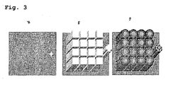
- Fig. 3 shows a possible lithographic production variant of a system with light barriers.
- the flat camera can ultimately be applied as a thin polymer layer to the electronics, which then serves as a substrate.
- the lenses are most diverse Technologies conceivable. For example, established technologies such as the reflow process (for round or elliptical lenses), imaging of UV-curable polymer (UV reaction casting) or etching (RIE) in glass can be used in micro-optics. Spheres and aspheres as lenses are possible. Other variants of the production can be embossing or printing on a plastic film.
- the lenses may be refractive, diffractive or refractive-diffractive (hybrid).
- the system can after injection of a polymer u. U. impressed directly on the electronics or otherwise molded.
- FIG. 4 shows an already realized variant embodiment.
- a 20 ⁇ m thick polymer layer 10 on the front side of a 300 ⁇ m thick glass substrate 11 contains the necessary microlenses.
- On the back side of the substrate is a pinhole array 12 of slightly lower pitches than the microlens array in a metal layer.
- This arrangement provides an image of the object with significantly greater magnification than can be observed behind an individual microlens, with a significantly shorter length than conventional lenses with comparable magnification.
- the substrate thickness is set equal to the focal length of the microlenses, so that the pinhole array is located in the image plane of the microlens array.
- the lens diameter is 85 microns, the size of the scanned field of view 60 microns x 60 microns, the pitch of the optical channels is 90 microns.
- the field of view for rotationally symmetrical lenses is the meaningful NA The lenses are limited from 0.19 to 15 ° along the diagonal.
- the number of optical channels is 101 x 101, which corresponds to the number of resulting pixels.
- the pinhole array needed to cover the detector array consists of low / minimal transmission material.
- metal coatings are particularly suitable.
- these have the disadvantage of high reflectivity, which leads to stray light within the system.
- Replacement of the metal layer with a black polymer structured with pinholes is advantageous for reducing the scattered light.
- a combination of black polymer layer and metal layer allows low transmission with low reflection.
- the microimage can only be meaningfully scanned as long as the scanning pinhole does not migrate out of the image area of the corresponding microlens.
- An enlargement of the image area can only mean using the largest possible filling factor for the microlens array that also the lens diameter (in a square arrangement the same Lens pitch p) must be increased.
- NA p / 2f
- FOV arctan (2NA)
- the size of the field of view of the arrangement described is thus determined by the size of the numerical aperture of the microlens. Any increase in the NA of the lenses is not possible due to the increase in the size of the aberrations, even using aspherical microlenses due to the large angle spectrum to be processed.
- ⁇ p a (1-N / (N-1)) where N is the number of cells in one dimension of the flat camera.
- the expansion of the field of view or reduction of the magnification by various methods described here and combinable with one another is an essential point of the present invention.
- Fig. 6 shows an inventive imaging system with a lens array of individual microlenses 14 and a detector array with individual detectors 15.
- the lens array is on a curved Surface arranged.
- the optical axes 13 are fanned out, whereby a visual field extension is achieved.
- Fig. 7 shows an image acquisition system according to the invention with a lens array with individual lenses 14 and a detector array with individual detectors 15 on a curved base.
- the focal lengths of the lenses can all be the same here.
- a diverging lens as a base surface is conceivable, the resulting overall image is then reversed.
- Essential here too is the optical isolation of the individual channels by means of suitable partitions for suppression of ghosting caused by crosstalk between adjacent channels.
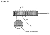
- Fig. 8 shows a side view of the image acquisition system according to the invention in planar design with a pixel of suitable size per channel. It consists of microlens array 18, distance-defining structure to the image plane and optical isolation 19 of the channels for suppressing crosstalk in a monolithic plate 20, which is placed directly on the image sensor 21. Due to a slightly smaller pitch of the pixels of the image sensor compared to that of the lens array, the relative position of the sensor pixel to the microlens is different in each channel, whereby the necessary variation of the viewing direction is achieved among the channels.
- the section shows the possible pixel position within the channel for a channel at the edge of the camera.
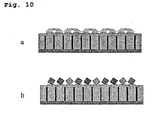
- Fig. 10 shows the integration of additional channel-to-channel optical functions into the plane of the microlens arrays. So shows Fig. 10a an integrated polarizing filter or a similar purpose grating, while in FIG. 10b is shown in integrated color filter.
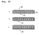
- Fig. 11 shows different variants for the geometric arrangement of the optical channels in the array.
- Fig. 11a is shown a Cartesian arrangement of the optical channels
- Fig. 11b a radially symmetric arrangement of the optical channels
- Fig. 11c a hexagonal arrangement of the optical channels is present.
Landscapes
- Physics & Mathematics (AREA)
- Optics & Photonics (AREA)
- Engineering & Computer Science (AREA)
- General Physics & Mathematics (AREA)
- Multimedia (AREA)
- Signal Processing (AREA)
- Manufacturing & Machinery (AREA)
- Human Computer Interaction (AREA)
- Theoretical Computer Science (AREA)
- Transforming Light Signals Into Electric Signals (AREA)
- Solid State Image Pick-Up Elements (AREA)
- Studio Devices (AREA)
- Transition And Organic Metals Composition Catalysts For Addition Polymerization (AREA)
- Polymerisation Methods In General (AREA)
- Lubrication Of Internal Combustion Engines (AREA)
Claims (36)
- Système d'acquisition d'image composé de canaux optiques disposés en réseau, avec une microlentille (14) et au moins un détecteur (15), situé dans le plan focal de celle-ci, qui extrait de la micro-image derrière la microlentille au moins un point d'image, ainsi qu'avec un diaphragme à trou (12) disposé éventuellement devant le détecteur, dans lequel les axes optiques (13) des canaux optiques individuels présentent des inclinaisons différentes de telle sorte qu'ils représentent une fonction de la distance du canal optique par rapport au centre du côté du système d'acquisition d'image tourné vers l'image, de sorte que le rapport entre la dimension du champ de vision et la dimension du champ d'image peut être déterminé précisément, et dans lequel des détecteurs (15) sont mis en oeuvre avec une sensibilité tellement élevée qu'ils présentent un pas élevé pour une petite surface active, dans lequel l'inclinaison variable des axes optiques des canaux optiques individuels est assurée en ce que la distance de centre à centre, c'est-à-dire le pas, des microlentilles est différente de la distance de centre à centre des détecteurs,
caractérisé en ce qu'au moins une partie des microlentilles sont des microlentilles anamorphosiques qui sont différentes pour chaque canal optique individuel, et en ce que le système optique composé d'un réseau de microlentilles moulées et de canaux optiques optiquement isolés les uns des autres est posé comme une structure monolithique directement sur le réseau de détecteurs. - Système d'acquisition d'image selon la revendication 1, caractérisé en ce que chaque canal optique acquiert au moins un segment angulaire solide déterminé de l'espace objet comme un point d'image correspondant de sorte que la totalité des points d'image transmis sur le réseau de détecteurs permet une reconstruction de l'objet.
- Système d'acquisition d'image selon l'une quelconque des revendications précédentes, caractérisé en ce que les microlentilles individuelles se distinguent au niveau du décentrage par rapport au détecteur, de la distance focale, des paramètres coniques et/ou asphériques, et permettent ainsi différentes inclinaisons des axes optiques.
- Système d'acquisition d'image selon l'une quelconque des revendications précédentes, caractérisé en ce que dans les microlentilles individuelles, des microprismes sont intégrés qui permettent différentes inclinaisons des axes optiques.
- Système d'acquisition d'image selon l'une quelconque des revendications précédentes, caractérisé en ce que pour les différentes inclinaisons des axes optiques, les canaux optiques sont exempts d'aberrations extra-axiales.
- Système d'acquisition d'image selon l'une quelconque des revendications précédentes, caractérisé en ce que les canaux optiques individuels présentent des différences de pas différentes entre la microlentille et le détecteur et/ou des trous sténopéiques pour corriger une distorsion d'image.
- Système d'acquisition d'image selon l'une quelconque des revendications précédentes, caractérisé en ce que le système d'acquisition d'image présente une longueur de construction de moins de 1 mm.
- Système d'acquisition d'image selon l'une quelconque des revendications précédentes, caractérisé en ce que le nombre des canaux optiques se situe dans la plage de 10 x 10 à 1000 x 1000.
- Système d'acquisition d'image selon l'une quelconque des revendications précédentes, caractérisé en ce que la dimension des canaux optiques se situe dans la plage de 10 µm x 10 µm à 1 mm x 1 mm.
- Système d'acquisition d'image selon l'une quelconque des revendications précédentes, caractérisé en ce que l'agencement régulier des canaux optiques est très compact de façon carrée ou hexagonale ou à symétrie de révolution.
- Système d'acquisition d'image selon l'une quelconque des revendications précédentes, caractérisé en ce que les positions des microlentilles et des détecteurs sont définies exactement par lithographie.
- Système d'acquisition d'image selon l'une quelconque des revendications précédentes, caractérisé en ce que l'isolation optique s'effectue par des cloisons réalisées par lithographie.
- Système d'acquisition d'image selon l'une quelconque des revendications précédentes, caractérisé en ce que les détecteurs se présentent sous forme d'un CCD, d'un réseau de photocapteurs CMOS et/ou d'un réseau de photocapteurs composé d'un polymère.
- Système d'acquisition d'image selon l'une quelconque des revendications précédentes, caractérisé en ce que les canaux optiques présentent respectivement plusieurs détecteurs de fonction différente.
- Système d'acquisition d'image selon l'une quelconque des revendications précédentes, caractérisé en ce que derrière les microlentilles et directement devant les détecteurs, des diaphragmes à trou sont disposés et positionnés de telle sorte que chaque microlentille se voit attribuer au moins un diaphragme à trou.
- Système d'acquisition d'image selon l'une quelconque des revendications précédentes, caractérisé en ce que le rapport entre la surface active du détecteur et la surface active de la microlentille pour définir l'intensité de lumière et le pouvoir de résolution est réglable par l'intermédiaire du diaphragme à trou.
- Système d'acquisition d'image selon l'une quelconque des revendications précédentes, caractérisé en ce que les diaphragmes à trou possèdent un diamètre dans la plage de 1 à 10 µm.
- Système d'acquisition d'image selon l'une des deux revendications précédentes, caractérisé en ce que le diaphragme à trou est réalisé à partir d'un revêtement de métal ou de polymère ou de combinaisons de ceux-ci.
- Système d'acquisition d'image selon l'une quelconque des revendications précédentes, caractérisé en ce que le système d'acquisition d'image présente de plus une lentille liquide placée en amont entre l'image et les microlentilles pour le réglage du champ de vision.
- Système d'acquisition d'image selon l'une quelconque des revendications précédentes, caractérisé en ce que des sources de lumière sont disposées sur ou entre les canaux optiques.
- Système d'acquisition d'image selon l'une quelconque des revendications précédentes, caractérisé en ce que chaque canal optique se voit attribuer un pixel.
- Système d'acquisition d'image selon l'une quelconque des revendications précédentes, caractérisé en ce que chaque canal optique se voit attribuer plusieurs pixels.
- Système d'acquisition d'image selon l'une quelconque des revendications précédentes, caractérisé en ce qu'il existe plusieurs pixels ayant différentes propriétés ou groupes de pixels de propriétés identiques.
- Système d'acquisition d'image selon l'une des deux revendications précédentes, caractérisé en ce que devant plusieurs pixels de même type, des filtres de couleur sont disposés.
- Système d'acquisition d'image selon l'une quelconque des revendications 22 à 24, caractérisé en ce que plusieurs pixels de même type avec une plus grande distance sont disposés dans un canal optique pour augmenter l'intensité lumineuse sans perte de résolution.
- Système d'acquisition d'image selon l'une quelconque des revendications 22 à 24, caractérisé en ce que les pixels multiples par canal optique sont disposés de telle sorte que les axes optiques d'au moins deux canaux optiques se coupent en un point objet afin de permettre une prise de vue 3D stéréoscopique et/ou une mesure de distance.
- Système d'acquisition d'image selon l'une quelconque des revendications 22 à 26, caractérisé en ce que devant ou sur les microlentilles, des éléments dispersifs sont disposés pour des prises de vue en couleur.
- Système d'acquisition d'image selon l'une quelconque des revendications 22 à 27, caractérisé en ce que devant des pixels de même type d'un canal optique, des réseaux d'orientation différente ou des filtres de polarisation structurés sont disposés pour le réglage de la sensibilité de polarisation.
- Système d'acquisition d'image selon l'une quelconque des revendications précédentes, caractérisé en ce que le système d'acquisition d'image est combiné avec au moins un élément à cristaux liquides.
- Utilisation du système d'acquisition d'image selon l'une quelconque des revendications 1 à 29 comme une partie intégrante dans des micro-appareils de construction plate, comme par exemple des horloges, des ordinateurs portables, des PDA ou organiseurs, des téléphones mobiles, des lunettes ou des vêtements.
- Utilisation du système d'acquisition d'image selon l'une quelconque des revendications 1 à 29 pour la surveillance, la technique de sécurité ainsi que pour le contrôle et la mise en oeuvre d'autorisations d'accès ou d'exploitation.
- Utilisation du système d'acquisition d'image selon l'une quelconque des revendications 1 à 29 comme un appareil photo sur une carte à puce, par exemple une carte de crédit.
- Utilisation du système d'acquisition d'image selon l'une quelconque des revendications 1 à 29 dans la technique médicale, par exemple pour l'endoscopie.
- Utilisation du système d'acquisition d'image selon l'une quelconque des revendications 1 à 29 comme un système de capteurs dans le domaine automobile, par exemple pour des tâches de surveillance à l'intérieur et à l'extérieur d'un véhicule.
- Utilisation du système d'acquisition d'image selon l'une quelconque des revendications 1 à 29 dans l'industrie aéronautique, par exemple pour la surveillance intégrée et intelligente du poste de pilotage.
- Utilisation du système d'acquisition d'image selon l'une quelconque des revendications 1 à 29 pour la reconnaissance d'un iris, la reconnaissance d'empreintes digitales, la reconnaissance d'objets et la détection de mouvement, en particulier le suivi de mouvement en 3D.
Applications Claiming Priority (2)
| Application Number | Priority Date | Filing Date | Title |
|---|---|---|---|
| DE102004003013A DE102004003013B3 (de) | 2004-01-20 | 2004-01-20 | Bilderfassungssystem und dessen Verwendung |
| PCT/EP2005/000495 WO2005069607A1 (fr) | 2004-01-20 | 2005-01-19 | Systeme de capture d'images et utilisation |
Publications (3)
| Publication Number | Publication Date |
|---|---|
| EP1665779A1 EP1665779A1 (fr) | 2006-06-07 |
| EP1665779B1 true EP1665779B1 (fr) | 2009-07-29 |
| EP1665779B8 EP1665779B8 (fr) | 2009-12-16 |
Family
ID=34530456
Family Applications (1)
| Application Number | Title | Priority Date | Filing Date |
|---|---|---|---|
| EP05706929A Expired - Lifetime EP1665779B8 (fr) | 2004-01-20 | 2005-01-19 | Systeme de capture d'images et son utilisation |
Country Status (6)
| Country | Link |
|---|---|
| US (1) | US20070109438A1 (fr) |
| EP (1) | EP1665779B8 (fr) |
| JP (1) | JP2007520743A (fr) |
| AT (1) | ATE438259T1 (fr) |
| DE (2) | DE102004003013B3 (fr) |
| WO (1) | WO2005069607A1 (fr) |
Cited By (2)
| Publication number | Priority date | Publication date | Assignee | Title |
|---|---|---|---|---|
| WO2011045324A2 (fr) | 2009-10-14 | 2011-04-21 | Fraunhofer-Gesellschaft zur Förderung der angewandten Forschung e.V. | Dispositif, dispositif de traitement d'images et procédé de reproduction optique |
| DE102017113554A1 (de) | 2017-06-20 | 2018-12-20 | HELLA GmbH & Co. KGaA | Verfahren zur Herstellung eines Verbundes aus einem Display und einer auf das Display aufgebrachten Optik |
Families Citing this family (111)
| Publication number | Priority date | Publication date | Assignee | Title |
|---|---|---|---|---|
| US20060215054A1 (en) * | 2005-03-23 | 2006-09-28 | Eastman Kodak Company | Wide angle camera with prism array |
| DE102005016818B4 (de) * | 2005-04-07 | 2007-09-27 | Fraunhofer-Gesellschaft zur Förderung der angewandten Forschung e.V. | Einrichtung zur optischen Verschlüsselung, Einrichtung zur optischen Entschlüsselung und Verschlüsselungs-/Entschlüsselungs-System |
| EP1764835B1 (fr) * | 2005-09-19 | 2008-01-23 | CRF Societa'Consortile per Azioni | Senseur optique multifonctionnel avec une matrice de photodétecteurs couplé aux microlentilles |
| DE102005059363B4 (de) * | 2005-12-13 | 2007-08-16 | Leuze Electronic Gmbh & Co Kg | Optischer Sensor |
| DE102006004802B4 (de) | 2006-01-23 | 2008-09-25 | Fraunhofer-Gesellschaft zur Förderung der angewandten Forschung e.V. | Bilderfassungssystem und Verfahren zur Herstellung mindestens eines Bilderfassungssystems |
| DE102006011540A1 (de) * | 2006-02-12 | 2007-08-23 | Samland, Thomas, Dipl.-Math. | Abtasteinheit für eine Positionsmesseinrichtung zur Detektion von optischen Maßverkörperungen sowie entsprechende Positionsmesseinrichtung |
| DE102006007764A1 (de) * | 2006-02-20 | 2007-08-23 | Sick Ag | Optoelektronische Vorrichtung und Verfahren zu deren Betrieb |
| DE102006019124B4 (de) * | 2006-04-25 | 2012-08-30 | Fraunhofer-Gesellschaft zur Förderung der angewandten Forschung e.V. | Bilderfassungssystem zur Rundumsicht |
| US7554743B2 (en) * | 2006-05-30 | 2009-06-30 | Wisconsin Alumni Research Foundation | Variable-focus lens assembly |
| JP2007329714A (ja) * | 2006-06-08 | 2007-12-20 | Funai Electric Co Ltd | 複眼撮像装置 |
| DE102006040657B4 (de) * | 2006-08-30 | 2016-05-12 | Robert Bosch Gmbh | Bilderfassungssystem für Anwendungen in Fahrzeugen |
| JP4172512B2 (ja) * | 2006-08-30 | 2008-10-29 | 船井電機株式会社 | パノラマ撮像装置 |
| JP2008064903A (ja) * | 2006-09-06 | 2008-03-21 | National Institute Of Advanced Industrial & Technology | 三次元構造物作製装置、センサー作製装置、及び三次元構造物作製方法 |
| DE102006060062A1 (de) * | 2006-12-19 | 2008-07-03 | Sick Ag | Objektfeststellungssensor |
| DE102007008756A1 (de) | 2007-02-22 | 2008-08-28 | Siemens Ag | Messkopf für ein Endoskop und Endoskop |
| US20100282316A1 (en) * | 2007-04-02 | 2010-11-11 | Solaria Corporation | Solar Cell Concentrator Structure Including A Plurality of Glass Concentrator Elements With A Notch Design |
| DE102007042984B4 (de) | 2007-09-10 | 2026-04-02 | Fraunhofer-Gesellschaft zur Förderung der angewandten Forschung e.V. | Vorrichtung zur optischen Navigation |
| US7672058B2 (en) * | 2007-09-17 | 2010-03-02 | Wisconsin Alumni Research Foundation | Compound eye |
| DE102007050167A1 (de) | 2007-10-19 | 2009-04-23 | Fraunhofer-Gesellschaft zur Förderung der angewandten Forschung e.V. | Mikrolinsen-Array mit integrierter Beleuchtung |
| WO2009090217A1 (fr) * | 2008-01-18 | 2009-07-23 | Axsionics Ag | Dispositif de caméra pour une acquisition d'image d' objets plats ou presque plats |
| US9494771B2 (en) | 2009-01-05 | 2016-11-15 | Duke University | Quasi-monocentric-lens-based multi-scale optical system |
| US9635253B2 (en) | 2009-01-05 | 2017-04-25 | Duke University | Multiscale telescopic imaging system |
| US9395617B2 (en) | 2009-01-05 | 2016-07-19 | Applied Quantum Technologies, Inc. | Panoramic multi-scale imager and method therefor |
| US8259212B2 (en) * | 2009-01-05 | 2012-09-04 | Applied Quantum Technologies, Inc. | Multiscale optical system |
| US10725280B2 (en) | 2009-01-05 | 2020-07-28 | Duke University | Multiscale telescopic imaging system |
| US9432591B2 (en) | 2009-01-05 | 2016-08-30 | Duke University | Multiscale optical system having dynamic camera settings |
| US8300108B2 (en) | 2009-02-02 | 2012-10-30 | L-3 Communications Cincinnati Electronics Corporation | Multi-channel imaging devices comprising unit cells |
| KR100998017B1 (ko) * | 2009-02-23 | 2010-12-03 | 삼성엘이디 주식회사 | 발광소자 패키지용 렌즈 및 이를 구비하는 발광소자 패키지 |
| US20150077627A1 (en) * | 2009-02-23 | 2015-03-19 | Gary Edwin Sutton | Curved sensor formed from silicon fibers |
| US20100286476A1 (en) * | 2009-05-05 | 2010-11-11 | Hongrui Jiang | Endoscope With Tunable-Focus Microlens |
| ATE538406T1 (de) * | 2009-09-30 | 2012-01-15 | Fraunhofer Ges Forschung | Verfahren zur herstellung eines künstliches facettenauges |
| EP2588911B1 (fr) | 2010-04-27 | 2018-06-06 | Duke University | Systèmes optiques à échelles multiples basés sur une lentille monocentrique et procédés d'utilisation |
| DE102010031535A1 (de) | 2010-07-19 | 2012-01-19 | Fraunhofer-Gesellschaft zur Förderung der angewandten Forschung e.V. | Bildaufnahmevorrichtung und Verfahren zum Aufnehmen eines Bildes |
| JP5621615B2 (ja) * | 2011-01-21 | 2014-11-12 | 株式会社リコー | 撮像装置 |
| JP2012198191A (ja) * | 2011-03-07 | 2012-10-18 | Ricoh Co Ltd | 遠赤外線検出装置 |
| DE102011052802B4 (de) * | 2011-08-18 | 2014-03-13 | Sick Ag | 3D-Kamera und Verfahren zur Überwachung eines Raumbereichs |
| JP2013044885A (ja) * | 2011-08-23 | 2013-03-04 | Hitachi High-Technologies Corp | 拡大系イメージング装置及びイメージセンサ |
| WO2013044149A1 (fr) * | 2011-09-21 | 2013-03-28 | Aptina Imaging Corporation | Capteurs d'image dotés de multiples lentilles ayant des polarisations variables |
| DE102012215408A1 (de) * | 2012-08-30 | 2014-03-06 | Robert Bosch Gmbh | Vorrichtung zur Fahrzeugvermessung |
| US9389342B2 (en) | 2013-03-07 | 2016-07-12 | Wisconsin Alumni Research Foundation | Variable focus lens system |
| US9880391B2 (en) * | 2013-10-01 | 2018-01-30 | Heptagon Micro Optics Pte. Ltd. | Lens array modules and wafer-level techniques for fabricating the same |
| US20150153156A1 (en) * | 2013-12-03 | 2015-06-04 | Mvm Electronics, Inc. | High spatial and spectral resolution snapshot imaging spectrometers using oblique dispersion |
| JP6446465B2 (ja) * | 2014-09-30 | 2018-12-26 | ミラマサービスインク | 入出力装置、入出力プログラム、および入出力方法 |
| US10732771B2 (en) | 2014-11-12 | 2020-08-04 | Shenzhen GOODIX Technology Co., Ltd. | Fingerprint sensors having in-pixel optical sensors |
| EP3029494A1 (fr) | 2014-12-02 | 2016-06-08 | Sick Ag | Capteur optoélectronique |
| US10410037B2 (en) * | 2015-06-18 | 2019-09-10 | Shenzhen GOODIX Technology Co., Ltd. | Under-screen optical sensor module for on-screen fingerprint sensing implementing imaging lens, extra illumination or optical collimator array |
| CN107004130B (zh) * | 2015-06-18 | 2020-08-28 | 深圳市汇顶科技股份有限公司 | 用于屏幕上指纹感应的屏幕下光学传感器模块 |
| KR101928319B1 (ko) | 2015-06-18 | 2018-12-12 | 선전 구딕스 테크놀로지 컴퍼니, 리미티드 | 광 감지 능력을 가지는 다기능 지문 센서 |
| US10437974B2 (en) | 2015-06-18 | 2019-10-08 | Shenzhen GOODIX Technology Co., Ltd. | Optical sensing performance of under-screen optical sensor module for on-screen fingerprint sensing |
| US10410033B2 (en) * | 2015-06-18 | 2019-09-10 | Shenzhen GOODIX Technology Co., Ltd. | Under-LCD screen optical sensor module for on-screen fingerprint sensing |
| JP6703387B2 (ja) * | 2015-10-02 | 2020-06-03 | エルジー ディスプレイ カンパニー リミテッド | 薄膜光センサ、2次元アレイセンサ、および指紋センサ付きモバイル用ディスプレイ |
| EP3248141A4 (fr) | 2015-11-02 | 2018-01-03 | Shenzhen Goodix Technology Co., Ltd. | Capteur d'empreintes digitales multifonction doté d'une détection optique contre les contrefaçons d'empreintes digitales |
| WO2016177914A1 (fr) * | 2015-12-09 | 2016-11-10 | Fotonation Limited | Système d'acquisition d'images |
| JP6724371B2 (ja) * | 2016-01-12 | 2020-07-15 | 大日本印刷株式会社 | 撮像モジュール、撮像装置 |
| US10108841B2 (en) * | 2016-03-31 | 2018-10-23 | Synaptics Incorporated | Biometric sensor with diverging optical element |
| DE102016013512A1 (de) | 2016-04-18 | 2017-11-09 | Kastriot Merlaku | Beleuchtungs-System für Kameras aller Art oder für Mobiltelefone mit Kamera |
| JP2017204578A (ja) * | 2016-05-12 | 2017-11-16 | 凸版印刷株式会社 | 固体撮像素子およびその製造方法 |
| KR102624789B1 (ko) | 2016-06-27 | 2024-01-16 | 삼성전자주식회사 | 생체 센서 및 생체 센서를 포함하는 전자 장치 |
| US20180012069A1 (en) * | 2016-07-06 | 2018-01-11 | Samsung Electronics Co., Ltd. | Fingerprint sensor, fingerprint sensor package, and fingerprint sensing system using light sources of display panel |
| CN109478083B (zh) * | 2016-07-18 | 2022-11-18 | 深圳市汇顶科技股份有限公司 | 具有力感测能力的光学指纹传感器 |
| US10270947B2 (en) | 2016-09-15 | 2019-04-23 | Microsoft Technology Licensing, Llc | Flat digital image sensor |
| JP6947438B2 (ja) | 2016-12-05 | 2021-10-13 | フォトニック センサーズ アンド アルゴリズムス,エセ.エレ. | マイクロレンズアレイ |
| EP3440594A4 (fr) * | 2017-01-04 | 2019-09-25 | Shenzhen Goodix Technology Co., Ltd. | Amélioration des performances de détection optique d'un module de capteur optique sous-écran pour détection d'empreinte digitale sur écran |
| US10614283B2 (en) | 2017-03-07 | 2020-04-07 | Shenzhen GOODIX Technology Co., Ltd. | Devices with peripheral task bar display zone and under-LCD screen optical sensor module for on-screen fingerprint sensing |
| CN107260121B (zh) * | 2017-06-14 | 2023-11-21 | 苏州四海通仪器有限公司 | 一种复眼眼底相机 |
| US10680121B2 (en) | 2017-06-15 | 2020-06-09 | Egis Technology Inc. | Optical fingerprint sensor and manufacturing method of sensing module thereof |
| US10613256B2 (en) * | 2017-08-11 | 2020-04-07 | Industrial Technology Research Institute | Biometric device |
| JP6963295B2 (ja) * | 2017-09-01 | 2021-11-05 | 学校法人東京電機大学 | 3次元情報取得装置 |
| US10930709B2 (en) | 2017-10-03 | 2021-02-23 | Lockheed Martin Corporation | Stacked transparent pixel structures for image sensors |
| US10510812B2 (en) | 2017-11-09 | 2019-12-17 | Lockheed Martin Corporation | Display-integrated infrared emitter and sensor structures |
| DE102017130298A1 (de) * | 2017-12-18 | 2019-06-19 | Bundesdruckerei Gmbh | Vorrichtung und Verfahren zum Messen von Bilddaten |
| SE1751613A1 (en) | 2017-12-21 | 2019-06-22 | Fingerprint Cards Ab | Biometric imaging device and method for manufacturing the biometric imaging device |
| US10652529B2 (en) | 2018-02-07 | 2020-05-12 | Lockheed Martin Corporation | In-layer Signal processing |
| US10979699B2 (en) | 2018-02-07 | 2021-04-13 | Lockheed Martin Corporation | Plenoptic cellular imaging system |
| US10690910B2 (en) | 2018-02-07 | 2020-06-23 | Lockheed Martin Corporation | Plenoptic cellular vision correction |
| US10951883B2 (en) | 2018-02-07 | 2021-03-16 | Lockheed Martin Corporation | Distributed multi-screen array for high density display |
| US10594951B2 (en) | 2018-02-07 | 2020-03-17 | Lockheed Martin Corporation | Distributed multi-aperture camera array |
| US11616941B2 (en) | 2018-02-07 | 2023-03-28 | Lockheed Martin Corporation | Direct camera-to-display system |
| US10838250B2 (en) | 2018-02-07 | 2020-11-17 | Lockheed Martin Corporation | Display assemblies with electronically emulated transparency |
| US10216975B1 (en) * | 2018-02-23 | 2019-02-26 | Shenzhen GOODIX Technology Co., Ltd. | Optical imaging via imaging lens and imaging pinhole in under-screen optical sensor module for on-screen fingerprint sensing in devices having organic light emitting diode (OLED) screens or other screens |
| US10303921B1 (en) * | 2018-02-26 | 2019-05-28 | Shenzhen GOODIX Technology Co., Ltd. | On-LCD screen optical fingerprint sensing based on optical imaging with lens-pinhole module and other optical designs |
| EP3766003A4 (fr) | 2018-03-15 | 2021-05-12 | Fingerprint Cards AB | Dispositif d'imagerie biométrique et procédé de fabrication de dispositif d'imagerie biométrique |
| CN112106058A (zh) | 2018-05-07 | 2020-12-18 | 光波触控有限公司 | 一种用于指纹检测的紧凑型光学传感器 |
| CN110175492B (zh) | 2018-07-20 | 2022-03-01 | 神盾股份有限公司 | 光学指纹感测装置 |
| KR20210042929A (ko) | 2018-08-15 | 2021-04-20 | 쓰리엠 이노베이티브 프로퍼티즈 컴파니 | 마이크로렌즈 어레이를 포함하는 광학 요소 |
| US10733413B2 (en) | 2018-08-29 | 2020-08-04 | Fingerprint Cards Ab | Optical in-display fingerprint sensor and method for manufacturing such a sensor |
| US11333748B2 (en) | 2018-09-17 | 2022-05-17 | Waymo Llc | Array of light detectors with corresponding array of optical elements |
| US10866413B2 (en) | 2018-12-03 | 2020-12-15 | Lockheed Martin Corporation | Eccentric incident luminance pupil tracking |
| CN109459741B (zh) * | 2018-12-07 | 2024-06-07 | 南京先进激光技术研究院 | 一种用于激光雷达系统的测量调试装置 |
| US11308309B2 (en) * | 2018-12-10 | 2022-04-19 | Synaptics Incorporated | Fingerprint sensor having an increased sensing area |
| US10698201B1 (en) | 2019-04-02 | 2020-06-30 | Lockheed Martin Corporation | Plenoptic cellular axis redirection |
| US10921450B2 (en) * | 2019-04-24 | 2021-02-16 | Aeye, Inc. | Ladar system and method with frequency domain shuttering |
| US11709121B2 (en) * | 2019-11-18 | 2023-07-25 | Spraying Systems Co. | Machine learning-based particle-laden flow field characterization |
| KR20210138184A (ko) * | 2020-05-11 | 2021-11-19 | 삼성디스플레이 주식회사 | 지문 센서, 및 그를 포함한 표시 장치 |
| CN113706398B (zh) * | 2020-05-22 | 2024-08-20 | 西北工业大学 | 在运动场景下生成高动态图像的装置及方法 |
| DE102020207302A1 (de) | 2020-06-10 | 2021-12-16 | Fraunhofer-Gesellschaft zur Förderung der angewandten Forschung eingetragener Verein | Vorrichtung und Verfahren zur Aufnahme eines projizierten Punktmusters in einer Anzeigevorrichtung |
| EP3922167A1 (fr) * | 2020-06-12 | 2021-12-15 | Optotune AG | Caméra et procédé de fonctionnement d'une caméra |
| US12434172B2 (en) | 2020-09-22 | 2025-10-07 | The Usa, As Represented By The Secretary, Dept. Of Health And Human Services | Methods and systems for managing fluid flow in containers |
| JP2022091358A (ja) * | 2020-12-09 | 2022-06-21 | ソニーセミコンダクタソリューションズ株式会社 | 撮像装置および電子機器 |
| CN112839149B (zh) * | 2020-12-31 | 2022-05-06 | 光沦科技(深圳)有限公司 | 异构微光学成像模块及其图像重建方法和装置 |
| DE102021108096A1 (de) | 2021-03-30 | 2022-10-06 | Sick Ag | Optoelektronischer Sensor und Verfahren zur Erfassung eines Objekts |
| DE202021101693U1 (de) | 2021-03-30 | 2022-07-01 | Sick Ag | Optoelektronischer Sensor zur Erfassung eines Objekts |
| CN114706088A (zh) * | 2021-07-22 | 2022-07-05 | 神盾股份有限公司 | 光学感测装置 |
| WO2023112479A1 (fr) | 2021-12-14 | 2023-06-22 | ソニーセミコンダクタソリューションズ株式会社 | Dispositif de réception de lumière et appareil électronique |
| US12510699B2 (en) | 2022-03-03 | 2025-12-30 | 3M Innovative Properties Company | Optical construction |
| US12484326B2 (en) * | 2022-09-11 | 2025-11-25 | Apple Inc. | Imaging array with directional response |
| DE102022127905A1 (de) | 2022-10-21 | 2024-05-02 | FEV Group GmbH | Mikrolinsenarray für einen bildprojektor |
| CN116500710B (zh) * | 2023-04-28 | 2025-09-09 | 电子科技大学 | 基于干涉臂组的微透镜阵列、成像系统及图像重建方法 |
| CN119165624B (zh) * | 2024-10-14 | 2025-09-23 | 北京理工大学 | 一种多孔径龙虾眼光学系统 |
| CN119575600B (zh) * | 2024-11-27 | 2026-04-07 | 吉林大学 | 一种大视场角的微型相机及其制备方法 |
| CN120315076B (zh) * | 2025-04-30 | 2026-04-07 | 深圳市闪妙科技有限公司 | 光学系统以及激光雷达 |
Citations (1)
| Publication number | Priority date | Publication date | Assignee | Title |
|---|---|---|---|---|
| EP0813079A2 (fr) * | 1996-06-14 | 1997-12-17 | Eastman Kodak Company | Un réseau de lentilles diffractive/réfringente avec une deuxième surface asphérique |
Family Cites Families (40)
| Publication number | Priority date | Publication date | Assignee | Title |
|---|---|---|---|---|
| US4175844A (en) * | 1975-10-19 | 1979-11-27 | Yeda Research & Development Co. Ltd. | Optical imaging system |
| IL48318A0 (en) * | 1975-10-19 | 1975-12-31 | Yeda Res & Dev | Thin optical imaging device |
| JPH0265386A (ja) * | 1988-08-31 | 1990-03-06 | Konica Corp | 固体撮像素子 |
| JP2566087B2 (ja) * | 1992-01-27 | 1996-12-25 | 株式会社東芝 | 有色マイクロレンズアレイ及びその製造方法 |
| JP3170847B2 (ja) * | 1992-02-14 | 2001-05-28 | キヤノン株式会社 | 固体撮像素子及びそれを用いた光学機器 |
| JP2742185B2 (ja) * | 1992-10-01 | 1998-04-22 | 松下電子工業株式会社 | 固体撮像装置 |
| JPH06133229A (ja) * | 1992-10-16 | 1994-05-13 | Fuji Photo Optical Co Ltd | マイクロレンズを有する固体撮像素子 |
| JPH0750401A (ja) * | 1993-08-06 | 1995-02-21 | Sony Corp | 固体撮像素子及びその製造方法 |
| US5521725A (en) * | 1993-11-05 | 1996-05-28 | Alliedsignal Inc. | Illumination system employing an array of microprisms |
| JPH07225303A (ja) * | 1993-12-16 | 1995-08-22 | Sharp Corp | マイクロレンズ基板及びそれを用いた液晶表示素子ならびに液晶プロジェクタ装置 |
| DE19545484C2 (de) * | 1995-12-06 | 2002-06-20 | Deutsche Telekom Ag | Bildaufnahmeeinrichtung |
| US6141048A (en) * | 1996-08-19 | 2000-10-31 | Eastman Kodak Company | Compact image capture device |
| US6137535A (en) * | 1996-11-04 | 2000-10-24 | Eastman Kodak Company | Compact digital camera with segmented fields of view |
| NO305728B1 (no) * | 1997-11-14 | 1999-07-12 | Reidar E Tangen | Optoelektronisk kamera og fremgangsmÕte ved bildeformatering i samme |
| JP3462736B2 (ja) * | 1997-11-17 | 2003-11-05 | ペンタックス株式会社 | 固体撮像素子 |
| JP3209180B2 (ja) * | 1998-05-26 | 2001-09-17 | 日本電気株式会社 | 固体撮像装置の製造方法 |
| FR2782843B1 (fr) * | 1998-08-25 | 2000-09-29 | Commissariat Energie Atomique | Procede d'isolation physique de regions d'une plaque de substrat |
| JP2000271940A (ja) * | 1999-03-23 | 2000-10-03 | Canon Inc | マイクロレンズまたはマイクロレンズ金型の作製方法、それに用いるマイクロレンズ用またはマイクロレンズ金型用基板 |
| DE19917890A1 (de) * | 1999-04-20 | 2000-11-30 | Siemens Ag | Flachbauendes Bilderfassungssystem |
| JP3821614B2 (ja) * | 1999-08-20 | 2006-09-13 | 独立行政法人科学技術振興機構 | 画像入力装置 |
| US7027719B1 (en) * | 1999-10-08 | 2006-04-11 | Raytheon Company | Catastrophic event-survivable video recorder system |
| JP3571982B2 (ja) * | 2000-01-27 | 2004-09-29 | キヤノン株式会社 | 固体撮像装置及びそれを備えた固体撮像システム |
| US6995800B2 (en) * | 2000-01-27 | 2006-02-07 | Canon Kabushiki Kaisha | Image pickup apparatus utilizing a plurality of converging lenses |
| JP3684147B2 (ja) * | 2000-10-10 | 2005-08-17 | キヤノン株式会社 | マイクロ構造体アレイ、及びその作製方法 |
| DE10051763A1 (de) * | 2000-10-18 | 2002-05-08 | Tst Touchless Sensor Technolog | Kamera zur Aufzeichnung von Instrumenten im Cockpit eines Flugzeuges |
| EP1202080A3 (fr) * | 2000-10-31 | 2004-01-28 | Eastman Kodak Company | Réseau de microlentilles double face |
| US7351945B2 (en) * | 2001-04-27 | 2008-04-01 | Micron Technology, Inc. | Alignment among elements in an image sensor |
| JP3839271B2 (ja) * | 2001-05-01 | 2006-11-01 | 富士写真フイルム株式会社 | 固体撮像装置及びその製造方法 |
| US6987258B2 (en) * | 2001-12-19 | 2006-01-17 | Intel Corporation | Integrated circuit-based compound eye image sensor using a light pipe bundle |
| JP4004302B2 (ja) * | 2002-02-07 | 2007-11-07 | 富士フイルム株式会社 | 撮像素子 |
| US7196728B2 (en) * | 2002-03-27 | 2007-03-27 | Ericsson, Inc. | Method and apparatus for displaying images in combination with taking images |
| US20030214898A1 (en) * | 2002-04-15 | 2003-11-20 | Tetsuya Ogata | Optical pickup device and optical disk drive using the same |
| US6783900B2 (en) * | 2002-05-13 | 2004-08-31 | Micron Technology, Inc. | Color filter imaging array and method of formation |
| CZ2005209A3 (cs) * | 2002-09-10 | 2005-12-14 | Ivi Smart Technologies, Inc. | Bezpečné biometrické ověření identity |
| US7420231B2 (en) * | 2002-09-20 | 2008-09-02 | Sony Corporation | Solid state imaging pick-up device and method of manufacturing the same |
| JP4171786B2 (ja) * | 2002-10-25 | 2008-10-29 | コニカミノルタホールディングス株式会社 | 画像入力装置 |
| US7113336B2 (en) * | 2002-12-30 | 2006-09-26 | Ian Crosby | Microlens including wire-grid polarizer and methods of manufacture |
| US7274808B2 (en) * | 2003-04-18 | 2007-09-25 | Avago Technologies Ecbu Ip (Singapore)Pte Ltd | Imaging system and apparatus for combining finger recognition and finger navigation |
| JP2004333640A (ja) * | 2003-05-01 | 2004-11-25 | Olympus Corp | 可変光学素子、光学ユニット及び撮像装置 |
| JP4710610B2 (ja) * | 2003-08-22 | 2011-06-29 | コニカミノルタオプト株式会社 | 固体撮像装置及び該固体撮像装置を備えた撮像装置 |
-
2004
- 2004-01-20 DE DE102004003013A patent/DE102004003013B3/de not_active Expired - Fee Related
-
2005
- 2005-01-19 EP EP05706929A patent/EP1665779B8/fr not_active Expired - Lifetime
- 2005-01-19 US US10/581,943 patent/US20070109438A1/en not_active Abandoned
- 2005-01-19 DE DE502005007772T patent/DE502005007772D1/de not_active Expired - Lifetime
- 2005-01-19 AT AT05706929T patent/ATE438259T1/de not_active IP Right Cessation
- 2005-01-19 WO PCT/EP2005/000495 patent/WO2005069607A1/fr not_active Ceased
- 2005-01-19 JP JP2006548285A patent/JP2007520743A/ja active Pending
Patent Citations (1)
| Publication number | Priority date | Publication date | Assignee | Title |
|---|---|---|---|---|
| EP0813079A2 (fr) * | 1996-06-14 | 1997-12-17 | Eastman Kodak Company | Un réseau de lentilles diffractive/réfringente avec une deuxième surface asphérique |
Non-Patent Citations (1)
| Title |
|---|
| DUPARRÉ J.; SCHREIBER P.; VÖLKEL R.: "Theoretical analysis of an artificial superposition compound eye for application in ultra flat digital image acquisition devices", PROCEEDINGS OF THE SPIE CONFERENCE OPTICAL DESIGN AND ENGINEERING , ST ETIENNE, FRANCE 30.9.03-3.10.03, vol. 5249, 18 February 2004 (2004-02-18), SPIE,USA, pages 408 - 418 * |
Cited By (7)
| Publication number | Priority date | Publication date | Assignee | Title |
|---|---|---|---|---|
| WO2011045324A2 (fr) | 2009-10-14 | 2011-04-21 | Fraunhofer-Gesellschaft zur Förderung der angewandten Forschung e.V. | Dispositif, dispositif de traitement d'images et procédé de reproduction optique |
| WO2011045324A3 (fr) * | 2009-10-14 | 2011-06-23 | Fraunhofer-Gesellschaft zur Förderung der angewandten Forschung e.V. | Dispositif, dispositif de traitement d'images et procédé de reproduction optique |
| EP2429176A1 (fr) * | 2009-10-14 | 2012-03-14 | Fraunhofer-Gesellschaft zur Förderung der angewandten Forschung e.V. | Dispositif, dispositif de traitement d'image et procédé de représentation optique |
| EP2432213A1 (fr) * | 2009-10-14 | 2012-03-21 | Fraunhofer-Gesellschaft zur Förderung der angewandten Forschung e.V. | Dispositif, dispositif de traitement d'image et procédé de représentation optique |
| US8629930B2 (en) | 2009-10-14 | 2014-01-14 | Fraunhofer-Gesellschaft Zur Foerderung Der Angewandten Forschung E.V. | Device, image processing device and method for optical imaging |
| DE102009049387B4 (de) * | 2009-10-14 | 2016-05-25 | Fraunhofer-Gesellschaft zur Förderung der angewandten Forschung e.V. | Vorrichtung, Bildverarbeitungsvorrichtung und Verfahren zur optischen Abbildung |
| DE102017113554A1 (de) | 2017-06-20 | 2018-12-20 | HELLA GmbH & Co. KGaA | Verfahren zur Herstellung eines Verbundes aus einem Display und einer auf das Display aufgebrachten Optik |
Also Published As
| Publication number | Publication date |
|---|---|
| ATE438259T1 (de) | 2009-08-15 |
| EP1665779A1 (fr) | 2006-06-07 |
| WO2005069607A1 (fr) | 2005-07-28 |
| US20070109438A1 (en) | 2007-05-17 |
| DE102004003013B3 (de) | 2005-06-02 |
| DE502005007772D1 (de) | 2009-09-10 |
| EP1665779B8 (fr) | 2009-12-16 |
| JP2007520743A (ja) | 2007-07-26 |
Similar Documents
| Publication | Publication Date | Title |
|---|---|---|
| EP1665779B1 (fr) | Systeme de capture d'images et son utilisation | |
| EP2429176B1 (fr) | Dispositif de traitement d'image | |
| Cheng et al. | Review of state-of-the-art artificial compound eye imaging systems | |
| DE102006004802B4 (de) | Bilderfassungssystem und Verfahren zur Herstellung mindestens eines Bilderfassungssystems | |
| EP2164713B1 (fr) | Élément de sécurité | |
| DE102004044459B4 (de) | Sicherheitsdokument mit transparenten Fenstern | |
| EP1779166B1 (fr) | Module de camera à échelle de tranche, réseau de modules de caméras et procédé de production | |
| EP2011331B1 (fr) | Système de saisie d'image fournissant une vue panoramique | |
| DE69703461T2 (de) | Chipkartenleser mit Anzeigevorrichtung | |
| DE19755565A1 (de) | Linsenanordnungssystem | |
| WO2017029372A1 (fr) | Dispositif de représentation à ouvertures multiples avec substrat optique | |
| EP2627517A2 (fr) | Procédé de production d'un document de sécurité muni d'une caractéristique de sécurité dépendant de l'angle d'observation et document de sécurité correspondant | |
| DE102017218722A1 (de) | Umfelderfassungssystem zum Erfassen eines Umfelds eines Fahrzeugs und Verfahren zum Erfassen eines Umfelds eines Fahrzeugs | |
| DE102017011352A1 (de) | Kameramodul für digitalaufnahmen | |
| WO2000064146A2 (fr) | Systeme de detection d'images plat | |
| DE102011017355B4 (de) | Multifokales Abbildungssystem mit optischen Filtern | |
| EP3849819A1 (fr) | Document de securite et procede de production d'un tel document de securite | |
| US20240089579A1 (en) | Optical system with localized magnification | |
| DE102005033746A1 (de) | Kompaktes Objektiv zur digitalen Bilderfassung sowie Bilderfassungsvorrichtung | |
| CN212460096U (zh) | 一种基于微光学的动态编码防伪结构 | |
| AU2021402665A9 (en) | Methods for designing and producing a security feature | |
| WO2021094314A1 (fr) | Objectif, utilisation d'un objectif et système de mesure | |
| DE102020207302A1 (de) | Vorrichtung und Verfahren zur Aufnahme eines projizierten Punktmusters in einer Anzeigevorrichtung | |
| CH702414B1 (de) | Lesehilfe. |
Legal Events
| Date | Code | Title | Description |
|---|---|---|---|
| PUAI | Public reference made under article 153(3) epc to a published international application that has entered the european phase |
Free format text: ORIGINAL CODE: 0009012 |
|
| 17P | Request for examination filed |
Effective date: 20060324 |
|
| AK | Designated contracting states |
Kind code of ref document: A1 Designated state(s): AT BE BG CH CY CZ DE DK EE ES FI FR GB GR HU IE IS IT LI LT LU MC NL PL PT RO SE SI SK TR |
|
| DAX | Request for extension of the european patent (deleted) | ||
| 17Q | First examination report despatched |
Effective date: 20070928 |
|
| GRAP | Despatch of communication of intention to grant a patent |
Free format text: ORIGINAL CODE: EPIDOSNIGR1 |
|
| GRAS | Grant fee paid |
Free format text: ORIGINAL CODE: EPIDOSNIGR3 |
|
| GRAA | (expected) grant |
Free format text: ORIGINAL CODE: 0009210 |
|
| AK | Designated contracting states |
Kind code of ref document: B1 Designated state(s): AT BE BG CH CY CZ DE DK EE ES FI FR GB GR HU IE IS IT LI LT LU MC NL PL PT RO SE SI SK TR |
|
| REG | Reference to a national code |
Ref country code: GB Ref legal event code: FG4D Free format text: NOT ENGLISH |
|
| REG | Reference to a national code |
Ref country code: CH Ref legal event code: EP |
|
| REG | Reference to a national code |
Ref country code: IE Ref legal event code: FG4D |
|
| REF | Corresponds to: |
Ref document number: 502005007772 Country of ref document: DE Date of ref document: 20090910 Kind code of ref document: P |
|
| REG | Reference to a national code |
Ref country code: SE Ref legal event code: TRGR |
|
| RIN2 | Information on inventor provided after grant (corrected) |
Inventor name: BRAEUER, ANDREAS Inventor name: VOELKEL, REINHARD Inventor name: DANNBERG, PETER Inventor name: DUPARRE, JACQUES Inventor name: SCHREIBER, PETER |
|
| PG25 | Lapsed in a contracting state [announced via postgrant information from national office to epo] |
Ref country code: LT Free format text: LAPSE BECAUSE OF FAILURE TO SUBMIT A TRANSLATION OF THE DESCRIPTION OR TO PAY THE FEE WITHIN THE PRESCRIBED TIME-LIMIT Effective date: 20090729 Ref country code: IS Free format text: LAPSE BECAUSE OF FAILURE TO SUBMIT A TRANSLATION OF THE DESCRIPTION OR TO PAY THE FEE WITHIN THE PRESCRIBED TIME-LIMIT Effective date: 20091129 Ref country code: ES Free format text: LAPSE BECAUSE OF FAILURE TO SUBMIT A TRANSLATION OF THE DESCRIPTION OR TO PAY THE FEE WITHIN THE PRESCRIBED TIME-LIMIT Effective date: 20091109 |
|
| PG25 | Lapsed in a contracting state [announced via postgrant information from national office to epo] |
Ref country code: PL Free format text: LAPSE BECAUSE OF FAILURE TO SUBMIT A TRANSLATION OF THE DESCRIPTION OR TO PAY THE FEE WITHIN THE PRESCRIBED TIME-LIMIT Effective date: 20090729 Ref country code: SI Free format text: LAPSE BECAUSE OF FAILURE TO SUBMIT A TRANSLATION OF THE DESCRIPTION OR TO PAY THE FEE WITHIN THE PRESCRIBED TIME-LIMIT Effective date: 20090729 |
|
| REG | Reference to a national code |
Ref country code: IE Ref legal event code: FD4D |
|
| PG25 | Lapsed in a contracting state [announced via postgrant information from national office to epo] |
Ref country code: PT Free format text: LAPSE BECAUSE OF FAILURE TO SUBMIT A TRANSLATION OF THE DESCRIPTION OR TO PAY THE FEE WITHIN THE PRESCRIBED TIME-LIMIT Effective date: 20091129 Ref country code: BG Free format text: LAPSE BECAUSE OF FAILURE TO SUBMIT A TRANSLATION OF THE DESCRIPTION OR TO PAY THE FEE WITHIN THE PRESCRIBED TIME-LIMIT Effective date: 20091029 |
|
| PG25 | Lapsed in a contracting state [announced via postgrant information from national office to epo] |
Ref country code: RO Free format text: LAPSE BECAUSE OF FAILURE TO SUBMIT A TRANSLATION OF THE DESCRIPTION OR TO PAY THE FEE WITHIN THE PRESCRIBED TIME-LIMIT Effective date: 20090729 Ref country code: IE Free format text: LAPSE BECAUSE OF FAILURE TO SUBMIT A TRANSLATION OF THE DESCRIPTION OR TO PAY THE FEE WITHIN THE PRESCRIBED TIME-LIMIT Effective date: 20090729 Ref country code: EE Free format text: LAPSE BECAUSE OF FAILURE TO SUBMIT A TRANSLATION OF THE DESCRIPTION OR TO PAY THE FEE WITHIN THE PRESCRIBED TIME-LIMIT Effective date: 20090729 Ref country code: DK Free format text: LAPSE BECAUSE OF FAILURE TO SUBMIT A TRANSLATION OF THE DESCRIPTION OR TO PAY THE FEE WITHIN THE PRESCRIBED TIME-LIMIT Effective date: 20090729 Ref country code: CZ Free format text: LAPSE BECAUSE OF FAILURE TO SUBMIT A TRANSLATION OF THE DESCRIPTION OR TO PAY THE FEE WITHIN THE PRESCRIBED TIME-LIMIT Effective date: 20090729 |
|
| PG25 | Lapsed in a contracting state [announced via postgrant information from national office to epo] |
Ref country code: SK Free format text: LAPSE BECAUSE OF FAILURE TO SUBMIT A TRANSLATION OF THE DESCRIPTION OR TO PAY THE FEE WITHIN THE PRESCRIBED TIME-LIMIT Effective date: 20090729 |
|
| PLBE | No opposition filed within time limit |
Free format text: ORIGINAL CODE: 0009261 |
|
| STAA | Information on the status of an ep patent application or granted ep patent |
Free format text: STATUS: NO OPPOSITION FILED WITHIN TIME LIMIT |
|
| 26N | No opposition filed |
Effective date: 20100503 |
|
| BERE | Be: lapsed |
Owner name: FRAUNHOFER-GESELLSCHAFT ZUR FORDERUNG DER ANGEWAN Effective date: 20100131 |
|
| PG25 | Lapsed in a contracting state [announced via postgrant information from national office to epo] |
Ref country code: MC Free format text: LAPSE BECAUSE OF NON-PAYMENT OF DUE FEES Effective date: 20100131 |
|
| REG | Reference to a national code |
Ref country code: CH Ref legal event code: PL |
|
| PG25 | Lapsed in a contracting state [announced via postgrant information from national office to epo] |
Ref country code: CH Free format text: LAPSE BECAUSE OF NON-PAYMENT OF DUE FEES Effective date: 20100131 Ref country code: GR Free format text: LAPSE BECAUSE OF FAILURE TO SUBMIT A TRANSLATION OF THE DESCRIPTION OR TO PAY THE FEE WITHIN THE PRESCRIBED TIME-LIMIT Effective date: 20091030 Ref country code: LI Free format text: LAPSE BECAUSE OF NON-PAYMENT OF DUE FEES Effective date: 20100131 |
|
| PG25 | Lapsed in a contracting state [announced via postgrant information from national office to epo] |
Ref country code: BE Free format text: LAPSE BECAUSE OF NON-PAYMENT OF DUE FEES Effective date: 20100131 |
|
| PG25 | Lapsed in a contracting state [announced via postgrant information from national office to epo] |
Ref country code: AT Free format text: LAPSE BECAUSE OF NON-PAYMENT OF DUE FEES Effective date: 20100119 |
|
| PG25 | Lapsed in a contracting state [announced via postgrant information from national office to epo] |
Ref country code: CY Free format text: LAPSE BECAUSE OF FAILURE TO SUBMIT A TRANSLATION OF THE DESCRIPTION OR TO PAY THE FEE WITHIN THE PRESCRIBED TIME-LIMIT Effective date: 20090729 |
|
| PG25 | Lapsed in a contracting state [announced via postgrant information from national office to epo] |
Ref country code: HU Free format text: LAPSE BECAUSE OF FAILURE TO SUBMIT A TRANSLATION OF THE DESCRIPTION OR TO PAY THE FEE WITHIN THE PRESCRIBED TIME-LIMIT Effective date: 20100130 Ref country code: LU Free format text: LAPSE BECAUSE OF NON-PAYMENT OF DUE FEES Effective date: 20100119 |
|
| PG25 | Lapsed in a contracting state [announced via postgrant information from national office to epo] |
Ref country code: TR Free format text: LAPSE BECAUSE OF FAILURE TO SUBMIT A TRANSLATION OF THE DESCRIPTION OR TO PAY THE FEE WITHIN THE PRESCRIBED TIME-LIMIT Effective date: 20090729 |
|
| REG | Reference to a national code |
Ref country code: FR Ref legal event code: PLFP Year of fee payment: 12 |
|
| REG | Reference to a national code |
Ref country code: FR Ref legal event code: PLFP Year of fee payment: 13 |
|
| REG | Reference to a national code |
Ref country code: FR Ref legal event code: PLFP Year of fee payment: 14 |
|
| PGFP | Annual fee paid to national office [announced via postgrant information from national office to epo] |
Ref country code: FI Payment date: 20210119 Year of fee payment: 17 Ref country code: NL Payment date: 20210120 Year of fee payment: 17 |
|
| PGFP | Annual fee paid to national office [announced via postgrant information from national office to epo] |
Ref country code: SE Payment date: 20210122 Year of fee payment: 17 |
|
| REG | Reference to a national code |
Ref country code: FI Ref legal event code: MAE |
|
| REG | Reference to a national code |
Ref country code: SE Ref legal event code: EUG |
|
| REG | Reference to a national code |
Ref country code: NL Ref legal event code: MM Effective date: 20220201 |
|
| PG25 | Lapsed in a contracting state [announced via postgrant information from national office to epo] |
Ref country code: SE Free format text: LAPSE BECAUSE OF NON-PAYMENT OF DUE FEES Effective date: 20220120 Ref country code: NL Free format text: LAPSE BECAUSE OF NON-PAYMENT OF DUE FEES Effective date: 20220201 Ref country code: FI Free format text: LAPSE BECAUSE OF NON-PAYMENT OF DUE FEES Effective date: 20220119 |
|
| REG | Reference to a national code |
Ref country code: DE Ref legal event code: R079 Ref document number: 502005007772 Country of ref document: DE Free format text: PREVIOUS MAIN CLASS: H04N0005335000 Ipc: H04N0025000000 |
|
| P01 | Opt-out of the competence of the unified patent court (upc) registered |
Effective date: 20230524 |
|
| PGFP | Annual fee paid to national office [announced via postgrant information from national office to epo] |
Ref country code: DE Payment date: 20240119 Year of fee payment: 20 Ref country code: GB Payment date: 20240124 Year of fee payment: 20 |
|
| PGFP | Annual fee paid to national office [announced via postgrant information from national office to epo] |
Ref country code: IT Payment date: 20240131 Year of fee payment: 20 Ref country code: FR Payment date: 20240123 Year of fee payment: 20 |
|
| REG | Reference to a national code |
Ref country code: DE Ref legal event code: R071 Ref document number: 502005007772 Country of ref document: DE |
|
| REG | Reference to a national code |
Ref country code: GB Ref legal event code: PE20 Expiry date: 20250118 |
|
| PG25 | Lapsed in a contracting state [announced via postgrant information from national office to epo] |
Ref country code: GB Free format text: LAPSE BECAUSE OF EXPIRATION OF PROTECTION Effective date: 20250118 |