EP1831862B1 - Siegeleinrichtung - Google Patents
Siegeleinrichtung Download PDFInfo
- Publication number
- EP1831862B1 EP1831862B1 EP20050850173 EP05850173A EP1831862B1 EP 1831862 B1 EP1831862 B1 EP 1831862B1 EP 20050850173 EP20050850173 EP 20050850173 EP 05850173 A EP05850173 A EP 05850173A EP 1831862 B1 EP1831862 B1 EP 1831862B1
- Authority
- EP
- European Patent Office
- Prior art keywords
- seal
- circuit
- antenna
- connection
- contact
- Prior art date
- Legal status (The legal status is an assumption and is not a legal conclusion. Google has not performed a legal analysis and makes no representation as to the accuracy of the status listed.)
- Expired - Lifetime
Links
Images

Classifications
-
- G—PHYSICS
- G09—EDUCATION; CRYPTOGRAPHY; DISPLAY; ADVERTISING; SEALS
- G09F—DISPLAYING; ADVERTISING; SIGNS; LABELS OR NAME-PLATES; SEALS
- G09F3/00—Labels, tag tickets, or similar identification or indication means; Seals; Postage or like stamps
- G09F3/02—Forms or constructions
- G09F3/03—Forms or constructions of security seals
- G09F3/0305—Forms or constructions of security seals characterised by the type of seal used
- G09F3/0347—Forms or constructions of security seals characterised by the type of seal used having padlock-type sealing means
- G09F3/0358—Forms or constructions of security seals characterised by the type of seal used having padlock-type sealing means using a rigid hasp lock
-
- G—PHYSICS
- G06—COMPUTING OR CALCULATING; COUNTING
- G06K—GRAPHICAL DATA READING; PRESENTATION OF DATA; RECORD CARRIERS; HANDLING RECORD CARRIERS
- G06K19/00—Record carriers for use with machines and with at least a part designed to carry digital markings
- G06K19/06—Record carriers for use with machines and with at least a part designed to carry digital markings characterised by the kind of the digital marking, e.g. shape, nature, code
- G06K19/067—Record carriers with conductive marks, printed circuits or semiconductor circuit elements, e.g. credit or identity cards also with resonating or responding marks without active components
- G06K19/07—Record carriers with conductive marks, printed circuits or semiconductor circuit elements, e.g. credit or identity cards also with resonating or responding marks without active components with integrated circuit chips
- G06K19/077—Constructional details, e.g. mounting of circuits in the carrier
- G06K19/07749—Constructional details, e.g. mounting of circuits in the carrier the record carrier being capable of non-contact communication, e.g. constructional details of the antenna of a non-contact smart card
- G06K19/07798—Constructional details, e.g. mounting of circuits in the carrier the record carrier being capable of non-contact communication, e.g. constructional details of the antenna of a non-contact smart card part of the antenna or the integrated circuit being adapted for rupturing or breaking, e.g. record carriers functioning as sealing devices for detecting not-authenticated opening of containers
-
- G—PHYSICS
- G09—EDUCATION; CRYPTOGRAPHY; DISPLAY; ADVERTISING; SEALS
- G09F—DISPLAYING; ADVERTISING; SIGNS; LABELS OR NAME-PLATES; SEALS
- G09F3/00—Labels, tag tickets, or similar identification or indication means; Seals; Postage or like stamps
- G09F3/02—Forms or constructions
- G09F3/03—Forms or constructions of security seals
- G09F3/0305—Forms or constructions of security seals characterised by the type of seal used
- G09F3/0329—Forms or constructions of security seals characterised by the type of seal used having electronic sealing means
- G09F3/0335—Forms or constructions of security seals characterised by the type of seal used having electronic sealing means using RFID tags
-
- G—PHYSICS
- G09—EDUCATION; CRYPTOGRAPHY; DISPLAY; ADVERTISING; SEALS
- G09F—DISPLAYING; ADVERTISING; SIGNS; LABELS OR NAME-PLATES; SEALS
- G09F3/00—Labels, tag tickets, or similar identification or indication means; Seals; Postage or like stamps
- G09F3/02—Forms or constructions
- G09F3/03—Forms or constructions of security seals
- G09F3/0376—Forms or constructions of security seals using a special technique to detect tampering, e.g. by ultrasonic or optical means
-
- G—PHYSICS
- G09—EDUCATION; CRYPTOGRAPHY; DISPLAY; ADVERTISING; SEALS
- G09F—DISPLAYING; ADVERTISING; SIGNS; LABELS OR NAME-PLATES; SEALS
- G09F3/00—Labels, tag tickets, or similar identification or indication means; Seals; Postage or like stamps
- G09F3/02—Forms or constructions
- G09F3/03—Forms or constructions of security seals
- G09F3/0394—Forms or constructions of security seals with violation indication by generating a random number
-
- Y—GENERAL TAGGING OF NEW TECHNOLOGICAL DEVELOPMENTS; GENERAL TAGGING OF CROSS-SECTIONAL TECHNOLOGIES SPANNING OVER SEVERAL SECTIONS OF THE IPC; TECHNICAL SUBJECTS COVERED BY FORMER USPC CROSS-REFERENCE ART COLLECTIONS [XRACs] AND DIGESTS
- Y10—TECHNICAL SUBJECTS COVERED BY FORMER USPC
- Y10T—TECHNICAL SUBJECTS COVERED BY FORMER US CLASSIFICATION
- Y10T292/00—Closure fasteners
- Y10T292/48—Seals
- Y10T292/494—Interengaging shackle ends, inclosing housing
-
- Y—GENERAL TAGGING OF NEW TECHNOLOGICAL DEVELOPMENTS; GENERAL TAGGING OF CROSS-SECTIONAL TECHNOLOGIES SPANNING OVER SEVERAL SECTIONS OF THE IPC; TECHNICAL SUBJECTS COVERED BY FORMER USPC CROSS-REFERENCE ART COLLECTIONS [XRACs] AND DIGESTS
- Y10—TECHNICAL SUBJECTS COVERED BY FORMER USPC
- Y10T—TECHNICAL SUBJECTS COVERED BY FORMER US CLASSIFICATION
- Y10T292/00—Closure fasteners
- Y10T292/48—Seals
- Y10T292/507—Tag type
-
- Y—GENERAL TAGGING OF NEW TECHNOLOGICAL DEVELOPMENTS; GENERAL TAGGING OF CROSS-SECTIONAL TECHNOLOGIES SPANNING OVER SEVERAL SECTIONS OF THE IPC; TECHNICAL SUBJECTS COVERED BY FORMER USPC CROSS-REFERENCE ART COLLECTIONS [XRACs] AND DIGESTS
- Y10—TECHNICAL SUBJECTS COVERED BY FORMER USPC
- Y10T—TECHNICAL SUBJECTS COVERED BY FORMER US CLASSIFICATION
- Y10T292/00—Closure fasteners
- Y10T292/48—Seals
- Y10T292/509—Encasing
Definitions
- the present invention relates to a sealing device with a sealing body and a fastening device for captively securing the sealing body to a sealing object, wherein the fastening device is integrally connected at its one end to the sealing body and formed at its other end with a connecting device for non-positive connection with a seal body Connection device is provided.
- Sealing devices of the type mentioned are well known and are often referred to as "seals".
- the connecting device for non-positive connection of the fastening device with the sealing body is regularly formed as a non-detachable locking connection, which allows easy locking of the connecting device with a complementary trained on Siegelkötper connection device, but makes a non-destructive release of this connection impossible. This allows the known seals a visual inspection of the integrity of the seal.
- the resistance element consists of a random number of resistance wires, so that the resistance element has a randomly random resistance value.
- the EP-A-0 978 812 A2 describes a sealing device having a housing, an alarm circuit for generating an alarm signal and an alarm wire.
- the sealing body can selectively connect the alarm wire to the housing by means of closure elements. Using an external switch, the closing elements can be opened to release the wire from the housing.
- sealing means disclosed therein must comprise an internal power supply device, so that a dependence on an energy source is present and a limited service life is to be expected.
- the present invention has for its object to provide a sealing device, on the one hand allows easier verification of the integrity of the sealing device and on the other hand is characterized by increased security against manipulation. This object is achieved by a sealing device with the features of claim 1.
- the sealing body is provided with a designed as a circuit carrier with data transmission device, wherein the data carrier has an external circuit bridge, which extends to connect two connection points of the circuit through the fastening device.
- the connection points of the circuit is closed.
- the removal of the electrical contact thus leads to an interruption of a contact bridge of the circuit and to generate a data change on the disk, which can be read via the data transmission device from the outside.
- the data change may be temporary, ie exist only during the interruption of the contact bridge, or permanent nature, such that the data change due to the interruption of the contact bridge is maintained even after the contact has been restored, ie the circuit has a " Memory effect "has.
- the sealing device according to the invention is virtually forgery-proof.
- the circuit is provided with an antenna device arranged in the sealing device, which serves both as a data transmission device and for connection to an external power supply device.
- the circuit is designed as an integrated circuit, preferably as a chip.
- the design of the circuit as a chip allows a particularly simple integration of the circuit in the sealing body, for example, by a trained as a sealing body encapsulation of the chip or a chip receiving chip module.
- circuit bridge as a wire-shaped conductor allows an embodiment of the circuit bridge, which takes into account in a special way the function of the circuit bridge receiving fastening device for repositioning to a sealing object.
- the term "wire-shaped" is not to be understood as an indication of the formation of the circuit bridge in the manner of a conventional wire, but the term “wire-shaped” an elongated, directed execution of the electrical conductor in the manner of a wire imply.
- the circuit bridge may actually be designed as a wire sheathed by an insulation.
- the circuit bridge is connected in series with the antenna device.
- an external data access via the data transmission device designed as an antenna device after severing the circuit bridge as a result of a seal breakage no longer possible, so that the display of a seal break is indicated by the omission of the antenna signal.
- the circuit bridge itself can act as part of the antenna device in a particularly advantageous manner, so that the circuit bridge virtually forms a winding section of the antenna device.
- the circuit bridge is connected in parallel with the antenna device, so that even after the separation of the circuit bridge an antenna signal is given and thus can be made regardless of the state of the sealing device data transmission.
- an embodiment of the sealing device is possible, such that the circuit bridge is connected in series with a second antenna device, so that a severing of the circuit bridge has a direct effect on the range of the antenna signal. Also in the aforementioned embodiment, it is possible to form the circuit bridge as part of an antenna device, that is, consisting of a turn portion of the antenna device.
- the contact device For simple, without the need of using tools producible, electrically safe contact device between the connecting device at the end of the fastening device and the connection device on the seal body, it is advantageous to form the contact device as a latching connection device.
- the connecting device and / or the connecting device have a deformation part which thus deforms upon separation of the contact device in that the restoration of the frictional connection between the connecting device of the fastening device and the connecting device of the sealing body is not possible.
- the fastening device is designed as a wire conductor, a particularly simple construction of the fastening device is possible, since the wire conductor serves both as an electrical circuit bridge and as a mechanical fastening element for fastening the sealing body to the sealing object.
- a particularly simple embodiment of the entire sealing device is possible if the fastening device is formed from a one-piece extension of the sealing body, since thus the production of the fastening device and the sealing body can be carried out in a common molding process.
- the fastening device has a circuit bridge formed from conductive plastic
- the formation of the fastening device can be made in one piece with the sealing body by adding conductive particles into the plastic compound provided for producing the fastening device.
- a special protection against a restoration of the electrical conductor function after transection of the circuit bridge is achieved if the fastening device for forming the circuit bridge has a plurality of electrically conductive fibers, so that a Restoration of all fiber connections after transection of the fastening device is made virtually impossible.
- the circuit can be connected to a power supply device integrated in the sealing device, and the data transmission device can be formed from a data access contact arrangement arranged externally on the sealing body.
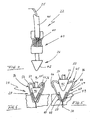
- Fig. 1 shows a sealing device 20 with a sealing body 21 and a fastening device 22.
- the sealing device 20 has in the illustrated simple embodiment as electrical components arranged in a seal body 21 chip module 23 with a chip not shown here and a contact surface arrangement 24, one for forming a circuit bridge in the wire conductor 25 arranged integrally with the sealing body 21 at one end 25 and a contact device 28 composed of a connecting device 26 at the free end of the fastening device 22 and a connecting device 27 arranged in the sealing body 21.
- the wire conductor 25 is connected to a first contact surface 29 of the contact surface arrangement 24.
- the connection device 27 is connected via a further wire conductor 30 contacted with a further contact surface 31 of the contact surface arrangement 24 of the chip module 23.
- Fig. 2 shows the sealing device 20 with closed contact device 28, wherein the at the end of the fastening device 22 and the wire conductor 25 formed electrically conductive connection means 26 is inserted into the connecting device 27.
- the wire conductor 25, together with the electrically connected via the contact device 28 wire conductor 30 as an antenna device 32 in addition to the formation of a contact surfaces 29 and 31 of the contact surface arrangement 24 interconnecting circuit bridge a data transmission device for non-contact connection of a reader not shown here forms with the data carrier formed by the chip of the chip module 23, not shown here.
- the antenna device 32 enables the energy supply necessary for the read-out process.
- a circuit configuration of the aforementioned type, comprising a chip module 23 and an antenna device 32 contacted with the chip module 23, is generally also referred to as a transponder.
- Fig. 3 shows according to another embodiment, a sealing device 33, which deviates from the in the Fig. 1 and 2 illustrated sealing device 20 has a chip module 34 which is provided with a contact surface arrangement 35.
- the contact surface arrangement 35 comprises, in addition to the contact surfaces 29, 31, which, as described above with reference to FIGS Fig. 1 and 2 already executed, are contacted with the wire conductors 25 and 30, further contact surfaces 36, 37 which are contacted with contact ends 38, 39 of a further antenna device 40.
- the in Fig. 3 illustrated sealing device 33 when the contact device 28 is closed, two antenna devices 32 and 40, wherein the function of the antenna device 40 is independent of whether the contact device 28 is opened or closed.
- the function of the antenna device 40 is independent of whether the formed by the wire conductor 25 in the fastening device 22 circuit bridge is closed or severed.
- Fig. 4 shows in an enlarged view the free end of the in the Fig. 1 to 3 shown fastening device 22 with the introduction into the also in the Fig. 1 to 3 illustrated connection device 27 certain connection means 26.
- the fastening device 22 of a one-piece to the seal body 21 ( FIG. Fig. 1 to 2 ) cast-on insulating Kunststoffummantclung 41 surrounded wire conductor 25 on.
- the connecting device 26 consists in the present case of a Ein 1500kegel 42 which is connected via a crimp connection 43 to a terminal end 44 of the wire conductor 25,
- FIGS. 5 and 6 show the insertion process for the production of the contact device 28 formed from the connection device 26 and the connection device 27 ( FIG. Fig. 5 ) as well as the finished contact device 28 ( Fig. 6 ).
- Fig. 5 shows, the firmly in the seal body 21, for example by gluing at least partially enclosed connection device 27 of a form-elastic, V-shaped, for example, made of plastic connection housing 51.
- the terminal housing 51 has two V-shaped employed and provided at their free end with locking clips 45 Expansion leg 46.
- a form complementary to Ein 1500kegel 42 trained conical contact 49 is arranged, which is connected with its contact tip 50 to the wire conductor 30.
- Fig. 5 is represented by an insertion of the Ein Siliconkegels 42 of the connecting device 26 in a formed between the locking brackets 45 of the terminal housing 51 insertion gap 52, a spreading of the expansion legs 46 causes.
- a spreading of the expansion legs 46 causes.
- the insertion of the Ein manufacturedkegel 42 enters the conical contact 49, and the trained at the end of the expansion limb 46 locking clip 45 engage around due to form elastic restoring forces of the expansion leg 46 the Ein manufacturedkegel 42 at its rear locking end 53rd
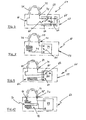
- sealing device 59 is a technical illustration and has arranged in a seal body 63, a chip module 64, which is contacted via a first pad arrangement 65 with a connecting conductor means 66 and a second pad arrangement 67 with an internal battery power supply device 68.
- the chip module 64 is provided with an externally accessible data access contact arrangement 69 arranged in the surface of the sealing body 63.
- the connecting conductor device 66 is connected to a circuit bridge 71 which is closed by a contact device 70 and which is arranged essentially in a fastening device 72 formed on the sealing body 63.
- Fig. 8 shows as an exemplary embodiment, the sealing device 60, which has arranged in the seal body 73, a chip module 74 which is contacted via a pad arrangement 75 with an antenna device 76.
- the antenna device 76 is likewise arranged in the sealing body 73 and on the one hand allows data access to the data stored in the chip of the chip module 74, not shown here, and on the other hand the power supply of the chip from outside the sealing body 73.
- Connected to the antenna device 76 is essentially a through a fastening device 77 extending circuit bridge 78 is connected, which is integrated with the contact device 70 closed in an antenna winding of the antenna device 76 and can increase the range of the antenna device 76 in a suitable embodiment.
- FIG. 9 illustrated embodiment of a sealing device 61 has a arranged in a seal body 79 chip module 80, which is connected via a first pad assembly 81 with an antenna device 82 and a second pad arrangement 83 with a circuit bridge 84, the contact surfaces 70 closed contact surfaces 85 and 86 of the pad arrangement 83 short-circuits each other.
- Sealing device 61 shown is both the data access function via an externally arranged, not shown here and communicating with the antenna device 82 reading device and the power supply function of the antenna device 82 regardless of the contact device 70 or the integrity of a fastening device 87 of the sealing device 61 extending through the circuit bridge 84th This makes it possible, even then, to read data from the chip of the chip module 80, which may include, for example, product information or delivery data of the object provided with the sealing device, if the circuit bridge 84 is not closed due to a severance or an opened contact device 70.
- FIG. 10 illustrated embodiment of a sealing device 62 has a chip module 88 which is contacted via a pad assembly 89 with a two-part antenna device 90, which is composed of two parallel antenna units 91 and 92.
- the antenna unit 91 connected to an antenna winding, has a circuit bridge 93, which runs essentially through a fastening device 95 connected to the sealing body 94.
- the contact device 70 is closed, the antenna unit 91 is thus in operation next to the antenna unit 92.
- the contact device 70 is opened or the circuit bridge 93 is forcibly severed, only the antenna unit 92 is in function.
- a reduction in the signal strength of the antenna signal or a reduction in the range of the antenna device 90 indicates that either the contact device 70 is not closed or the circuit bridge 93 is severed.
- a severed circuit bridge 93 is in the in Fig. 10 illustrated embodiment, a non-contact data access to the chip module 88 via the antenna unit 92 at a correspondingly reduced distance between the sealing device 62 and a reading device not shown here possible.
Landscapes
- Engineering & Computer Science (AREA)
- Physics & Mathematics (AREA)
- General Physics & Mathematics (AREA)
- Theoretical Computer Science (AREA)
- Computer Security & Cryptography (AREA)
- Microelectronics & Electronic Packaging (AREA)
- Computer Hardware Design (AREA)
- Details Of Aerials (AREA)
- Near-Field Transmission Systems (AREA)
- Seal Device For Vehicle (AREA)
- Connector Housings Or Holding Contact Members (AREA)
- Electrical Discharge Machining, Electrochemical Machining, And Combined Machining (AREA)
Description
- Die vorliegende Erfindung betrifft eine Siegeleinrichtung mit einem Siegelkörper und einer Befestigungseinrichtung zur verliersicheren Befestigung des Siegelkörpers an einem Siegelobjekt, wobei die Befestigungseinrichtung an ihrem einen Ende einstückig mit dem Siegelkörper verbunden ist und an ihrem weiteren Ende mit einer Verbindungseinrichtung zur kraftschlüssigen Verbindung mit einer am Siegelkörper ausgebildeten Anschlusseinrichtung versehen ist.
- Siegeleinrichtungen der eingangs genannten Art sind hinlänglich bekannt und werden oftmals auch als "Plomben" bezeichnet. Bei derartigen Plomben ist die Verbindungseinrichtung zur kraftschlüssigen Verbindung der Befestigungseinrichtung mit dem Siegelkörper regelmäßig als nicht lösbare Rastverbindung ausgebildet, die zwar ein leichtes Verrasten der Verbindungseinrichtung mit einer komplementär am Siegelkötper ausgebildeten Anschlusseinrichtung ermöglicht, jedoch ein zerstörungsfreies Lösen dieser Verbindung unmöglich macht. Hierdurch ermöglichen die bekannten Plomben eine visuelle Überprüfung der Unversehrtheit der Plombe.
- Insbesondere bei der Überprüfung einer großen Anzahl von mit konventionellen Plomben gesicherten Siegelobjekten erweist sich die zur Überprüfung der Unversehrtheit der Plomben notwendige Inaugenscheinnahme jeder einzelnen Plombe als sehr aufwendig. Darüber hinaus sind je nach Bauart konventioneller Plomben Manipulationen an einer aufgebrochenen Plombe, die die Unversehrtheit der Plombe vortäuschen sollen, nicht völlig ausgeschlossen, sondern häufig nur eine Frage des im Zusammenhang mit der Vornahme der Manipulation betriebenen Aufwands.
- Aus der
US 6 002 343 A geht eine Siegeleinrichtung mit einem Siegelkörper mit darin enthaltener Elektronik hervor, an der ein Widerstandselement angeschlossen ist, dessen Zerstörung durch die Elektronik des Schlüsselkörpers festgestellt werden kann. Hierbei besteht das Widerstandselement aus einer zufälligen Anzahl von Widerstandsdrähten, sodass das Widerstandselement einen statistisch zufälligen Widerstandswert besitzt. - Die
EP-A-0 978 812 A2 - Beiden Druckschriften ist gemeinsam, dass die darin offenbarten Siegeleinrichtungen eine interne Spannungsversorgungseinrichtung umfassen müssen, so dass eine Abhängigkeit von einer Energiequelle vorhanden ist und eine begrenzte Funktionsdauer zu erwarten ist.
- Der vorliegenden Erfindung liegt die Aufgabe zugrunde, eine Siegeleinrichtung vorzuschlagen, die einerseits eine leichtere Überprüfung der Unversehrtheit der Siegeleinrichtung ermöglicht und andererseits sich durch eine vergrößerte Sicherheit gegen Manipulationen auszeichnet. Diese Aufgabe wird durch eine Siegeleinrichtung mit den Merkmalen des Anspruchs 1 gelöst.
- Bei der erfindungsgemäßen Siegeleinrichtung ist der Siegelkörper mit einem als Schaltkreis ausgeführten Datenträger mit Datenübertragungseinrichtung versehen, wobei der Datenträger eine externe Schaltungsbrücke aufweist, die zur Verbindung von zwei Anschlussstellen des Schaltkreises durch die Befestigungseinrichtung verläuft.
- Infolge der Herstellung der kraftschlüssigen Verbindung zwischen der Verbindungseinrichtung der Befestigungseinrichtung und der am Siegelkörper ausgebildeten Anschlusseinrichtung wird ein elektrischer Kontakt zwischen den Anschlussstellen des Schaltkreises geschlossen. Die Aufhebung des elektrischen Kontakts führt somit zu einer Unterbrechung einer Kontaktbrücke des Schaltkreises und zur Erzeugung einer Datenänderung auf dem Datenträger, die über die Datenübertragungseinrichtung von außen ablesbar ist. Je nach Ausbildung des Schaltkreises kann die Datenänderung temporärer Natur sein, also lediglich während der Unterbrechung der Kontaktbrücke existent sein, oder permanenter Natur, derart, dass die aufgrund der Unterbrechung der Kontaktbrücke erfolgte Datenänderung auch nach Wiederherstellung des Kontakts erhalten bleibt, also der Schaltkreis einen "memory-effect" aufweist. Insbesondere im letzteren Fall ist somit die Möglichkeit gegeben, dass selbst nach Durchführung einer Manipulation an der Siegeleinrichtung und der Wiederherstellung der externen Schaltungsbrücke die Manipulation bei einem Datenzugriff auf den Datenträger über die Datenübertragungseinrichtung dokumentiert ist. Damit ist die erfindungsgemäße Siegeleinrichtung praktisch fälschungssicher.
- Erfindungsgemäß ist der Schaltkreis mit einer in der Siegeleinrichtung angeordneten Antenneneinrichtung versehen, die sowohl als Datenübertragungseinrichtung als auch zur Verbindung mit einer externen Energieversorgungseinrichtung dient. Hierdurch wird ein berührungsloser Datenzugriff auf die Daten des Datenträgers möglich, wobei zusätzlich aufgrund der nicht benötigten internen Energieversorgungseinrichtung ein besonders hoher Grad der Miniaturisierung und damit eine entsprechend kleine und darüber hinaus leichte Ausbildung des Siegelkörpers möglich wird.
- Gemäß einer vorteilhaften Ausführungsform ist der Schaltkreis als integrierter Schaltkreis, vorzugsweise als Chip, ausgeführt. Die Ausführung des Schaltkreises als Chip ermöglicht eine besonders einfache Integration des Schaltkreises in den Siegelkörper, beispielsweise durch einen als Siegelkörper ausgebildeten Verguss des Chips bzw. eines den Chip aufnehmenden Chipmoduls.
- Eine vorteilhafte Ausführung der Schaltungsbrücke als drahtförmiger Leiter ermöglicht eine Ausgestaltung der Schaltungsbrücke, die in besonderer Weise die Funktion der die Schaltungsbrücke aufnehmenden Befestigungseinrichtung zur Umbefestigung an einem Siegelobjekt berücksichtigt. Dabei ist der Begriff "drahtförmig" nicht als Hinweis auf die Ausbildung der Schaltungsbrücke nach Art eines konventionellen Drahtes zu verstehen, vielmehr soll der Begriff "drahtförmig" eine langgestreckte, gerichtete Ausführung des elektrischen Leiters nach Art eines Drahtes implizieren. So kann die Schaltungsbrücke einerseits tatsächlich als ein durch eine Isolation ummantelter Draht gestaltet sein. Andererseits ist es beispielsweise auch möglich, eine aus Kunststoff gebildete Befestigungseinrichtung zumindest im Bereich einer durchgehenden Faser mit leitfähigen Partikeln zu versetzen, um einen elektrischen Leiter zu realisieren.
- In einer besonders einfach aufgebauten Ausführungsform der Siegeleinrichtung ist die Schaltungsbrücke in Reihe mit der Antenneneinrichtung geschaltet. Bei dieser Ausführungsform ist ein externer Datenzugriff über die als Antenneneinrichtung ausgebildete Datenübertragungseinrichtung nach Durchtrennung der Schaltungsbrücke infolge eines Siegelbruchs nicht mehr möglich, so dass die Anzeige eines Siegelbruchs durch den Wegfall des Antennensignals angezeigt wird.
- Bei der vorgenannten Ausführungsform kann in besonders vorteilhafter Weise die Schaltungsbrücke selbst als Teil der Antenneneinrichtung wirken, so dass die Schaltungsbrücke quasi einen Windungsabschnitt der Antenneneinrichtung bildet.
- Bei einer weiteren Ausführungsform der Siegeleinrichtung ist die Schaltungsbrücke parallel mit der Antenneneinrichtung geschaltet, so dass auch nach erfolgter Durchtrennung der Schaltungsbrücke ein Antennensignal gegeben ist und somit unabhängig vom Zustand der Siegeleinrichtung eine Datenübertragung erfolgen kann.
- Weiterhin ist auch eine Ausführung der Siegeleinrichtung möglich, derart, dass die Schaltungsbrücke in Reihe mit einer zweiten Antenneneinrichtung geschaltet ist, so dass ein Durchtrennen der Schaltungsbrücke unmittelbar Auswirkung hat auf die Reichweite des Antennensignals. Auch bei der vorgenannten Ausführungsform ist es möglich, die Schaltungsbrücke als Teil einer Antenneneinrichtung, also aus einem Windungsabschnitt der Antenneneinrichtung bestehend, auszubilden.
- Zur einfachen, ohne die Notwendigkeit der Verwendung von Werkzeugen herstellbaren, elektrisch sicheren Kontakteinrichtung zwischen der Verbindungseinrichtung am Ende der Befestigungseinrichtung und der Anschlusseinrichtung am Siegelkörper ist es vorteilhaft, die Kontakteinrichtung als Rastverbindungseinrichtung auszubilden.
- Um parallel zur Überprüfung der Unversehrtheit des Siegels basierend auf einem elektrischen Signal auch eine visuelle Überprüfung der Unversehrtheit zu ermöglichen, ist es vorteilhaft, die Kontakteinrichtung unabhängig von der Art und Weise ihrer Ausbildung als nicht lösbare Verbindung auszuführen.
- Um eine unerwünschte Wiederherstellung der Siegelfunktion durch eine Wiederherstellung der Kontakteinrichtung zwischen der Verbindungseinrichtung der Befestigungseinrichtung und der Anschlusseinrichtung des Siegelkörpers verhindern zu können, ist es besonders vorteilhaft, wenn die Verbindungseinrichtung und/oder die Anschlusseinrichtung einen Deformationsteil aufweisen, der bei einer Trennung der Kontakteinrichtung so deformiert, dass die Wiederherstellung der kraftschlüssigen Verbindung zwischen der Verbindungseinrichtung der Befestigungseinrichtung und der Anschlusseinrichtung des Siegelkörpers nicht möglich ist.
- Wenn die Befestigungseinrichtung als Drahtleiter ausgebildet ist, ist ein besonders einfacher Aufbau der Befestigungseinrichtung möglich, da der Drahtleiter sowohl als elektrische Schaltungsbrücke als auch als mechanisches Befestigungselement zur Befestigung des Siegelkörpers am Siegelobjekt dient.
- Eine besonders einfache Ausgestaltung der gesamten Siegeleinrichtung wird möglich, wenn die Befestigungseinrichtung aus einem einstückigen Fortsatz des Siegelkörpers gebildet ist, da somit die Herstellung der Befestigungseinrichtung und des Siegelkörpers in einem gemeinsamen Formungsvorgang erfolgen kann.
- Wenn die Befestigungseinrichtung eine aus leitfähigem Kunststoff gebildete Schaltungsbrücke aufweist, kann die Ausbildung der Befestigungseinrichtung einstückig mit dem Siegelkörper durch einen Zusatz von leitfähigen Partikeln in die zur Herstellung der Befestigungseinrichtung vorgesehene Kunststoffmasse erfolgen.
- Einen besonderen Schutz gegen eine Wiederherstellung der elektrischen Leiterfunktion nach Durchtrennung der Schaltungsbrücke erzielt man, wenn die Befestigungseinrichtung zur Ausbildung der Schaltungsbrücke eine Mehrzahl von elektrisch leitfähigen Fasern aufweist, so dass eine Wiederherstellung sämtlicher Faserverbindungen nach Durchtrennung der Befestigungseinrichtung praktisch unmöglich gemacht wird.
- Des weiteren ist zusätzlich denkbar, dass der Schaltkreis an eine in die Siegeleinrichtung integrierte Energieversorgungseinrichtung angeschlossen werden kann, und die Datenübertragungseinrichtung aus einer außen am Siegelkörper angeordneten Datenzugriffskontaktanordnung ausgebildet sein kann. Mit dieser Möglichkeit ist ein kontaktbehafteter Datenzugriff auf die Daten des Datenträgers von außen gegeben, ohne dass eine externe Energieversorgung des Schaltkreises für den Datenexport in eine Leseeinrichtung notwendig wäre.
- Nachfolgend werden bevorzugte Ausführungsformen der Siegeleinrichtung anhand der Zeichnung näher erläutert.
- Es zeigen:
- Fig. 1
- eine Siegeleinrichtung eines Ausführungsbeispiels mit ei- ner an einem Siegelkörper angeordneten Befestigungsein- richtung und geöffneter Kontakteinrichtung;
- Fig. 2
- die in
Fig. 1 dargestellte Siegeleinrichtung mit geschlos- sener Kontakteinrichtung; - Fig. 3
- eine Siegeleinrichtung in einer weiteren Ausführungsform mit geschlossener Kontakteinrichtung;
- Fig. 4
- eine am freien Ende einer Befestigungseinrichtung ausge- bildete Verbindungseinrichtung;
- Fig. 5
- eine Verbindungseinrichtung beim Einführen in eine am Siegelkörper ausgebildete Anschlusseinrichtung zur Aus- bildung einer geschlossenen Kontakteinrichtung;
- Fig. 6
- die geschlossene Kontakteinrichtung;
- Fig. 7
- eine Siegeleinrichtung zur Veranschaulichung der techni- schen Lehre in schematischer Darstellung mit einem Chip- modul zur Ausbildung eines Datenträgers und einer auf dem Chipmodul angeordneten Außenkontakteinrichtung als Datenübertragungseinrichtung;
- Fig. 8
- eine weitere Siegeleinrichtung eines Ausführungsbeispiels in schematischer Darstellung mit einem Chipmodul als Datenträger und einer Antenneneinrichtung als Datenüber- tragungseinrichtung;
- Fig. 9
- eine Siegeleinrichtung in einer weiteren Ausführungsform mit einem Chipmodul als Datenträger und einer Antennen- einrichtung als Datenübertragungseinrichtung;
- Fig. 10
- eine weitere Siegeleinrichtung eines Ausführungsbeispiels in schematischer Darstellung mit einem Chipmodul als Datenträger und einer Antenneneinrichtung als Datenüber- tragungseinrichtung.
-
Fig. 1 zeigt eine Siegeleinrichtung 20 mit einem Siegelkörper 21 und einer Befestigungseinrichtung 22. Die Siegeleinrichtung 20 weist in der dargestellten einfachen Ausführungsform als elektrische Bauelemente ein im Siegelkörper 21 angeordnetes Chipmodul 23 mit einem hier nicht näher dargestellten Chip und einer Kontaktflächenanordnung 24, einen zur Ausbildung einer Schaltungsbrücke in der mit einem Ende 25 einstückig mit dem Siegelkörper 21 verbundenen Befestigungseinrichtung 22 angeordneten Drahtleiter 25 sowie einer Kontakteinrichtung 28, die aus einer Verbindungseinrichtung 26 am freien Ende der Befestigungseinrichtung 22 und einer im Siegelkörper 21 angeordneten Anschlusseinrichtung 27 zusammengesetzt ist. Der Drahtleiter 25 ist mit einer ersten Kontaktfläche 29 der Kontaktflächenanordnung 24 verbunden. Zur elektrischen Verbindung der Anschlusseinrichtung 27 mit dem Chipmodul 23 ist die Anschlusseinrichtung 27 über einen weiteren Drahtleiter 30 mit einer weiteren Kontaktfläche 31 der Kontaktflächenanordnung 24 des Chipmoduls 23 kontaktiert. -
Fig. 2 zeigt die Siegeleinrichtung 20 mit geschlossener Kontakteinrichtung 28, wobei die am Ende der Befestigungseinrichtung 22 bzw. des Drahtleiters 25 ausgebildete elektrisch leitfähige Verbindungseinrichtung 26 in die Anschlusseinrichtung 27 eingeführt ist. In dieser Konfiguration dient der Drahtleiter 25 zusammen mit dem über die Kontakteinrichtung 28 elektrisch angeschlossenen Drahtleiter 30 als eine Antenneneinrichtung 32, die neben der Ausbildung einer die Kontaktflächen 29 und 31 der Kontaktflächenanordnung 24 miteinander verbindenden Schaltungsbrücke eine Datenübertragungseinrichtung zur kontaktfreien Verbindung eines hier nicht näher dargestellten Lesegerätes mit dem durch den hier nicht näher dargestellten Chip des Chipmoduls 23 gebildeten Datenträger bildet. Zudem ermöglicht die Antenneneinrichtung 32 die für den Auslesevorgang notwendige Energieversorgung. Ein Schaltungsaufbau der vorstehend genannten Art, umfassend ein Chipmodul 23 und eine mit dem Chipmodul 23 kontaktierte Antenneneinrichtung 32, wird allgemein auch als Transponder bezeichnet. -
Fig. 3 zeigt gemäß einer weiteren Ausführungsform eine Siegeleinrichtung 33, die abweichend von der in denFig. 1 und 2 dargestellten Siegelcinrichtung 20 ein Chipmodul 34 aufweist, das mit einer Kontaktflächenanordnung 35 versehen ist. Die Kontaktflächenanordnung 35 umfasst neben den Kontaktflächen 29, 31, die, wie vorstehend unter Bezugnahme auf dieFig. 1 und 2 bereits ausgeführt, mit den Drahtleitern 25 bzw. 30 kontaktiert sind, weitere Kontaktflächen 36, 37, die mit Kontaktenden 38, 39 einer weiteren Antenneneinrichtung 40 kontaktiert sind. Somit weist die inFig. 3 dargestellte Siegeleinrichtung 33 bei geschlossener Kontakteinrichtung 28 zwei Antenneneinrichtungen 32 und 40 auf, wobei die Funktion der Antenneneinrichtung 40 unabhängig davon ist, ob die Kontakteinrichtung 28 geöffnet oder geschlossen ist. Darüber hinaus ist die Funktion der Antenneneinrichtung 40 unabhängig davon, ob die durch den Drahtleiter 25 in der Befestigungseinrichtung 22 gebildete Schaltungsbrücke geschlossen oder durchtrennt ist. -
Fig. 4 zeigt in einer vergrößerten Darstellung das freie Ende der in denFig. 1 bis 3 dargestellten Befestigungseinrichtung 22 mit der zur Einführung in die ebenfalls in denFig. 1 bis 3 dargestellte Anschlusseinrichtung 27 bestimmten Verbindungseinrichtung 26. Bei dem inFig. 4 dargestellten Ausführungsbeispiel weist die Befestigungseinrichtung 22 den von einer einstückig an den Siegelkörper 21 (Fig. 1 bis 2 ) angegossenen isolierenden Kunststoffummantclung 41 umgebenen Drahtleiter 25 auf. Die Verbindungseinrichtung 26 besteht im vorliegenden Fall aus einem Einführkegel 42, der über eine Quetschverbindung 43 an ein Anschlussende 44 des Drahtleiters 25 angeschlossen ist, - Die
Fig. 5 und 6 zeigen den Einführvorgang zur Herstellung der aus der Verbindungseinrichtung 26 und der Anschlusseinrichtung 27 gebildeten Kontakteinrichtung 28 (Fig. 5 ) sowie die fertiggestellte Kontakteinrichtung 28 (Fig. 6 ). WieFig. 5 zeigt, besteht die fest im Siegelkörper 21 beispielsweise durch Verklebung zumindest teilweise eingeschlossene Anschlusseinrichtung 27 aus einem formelastischen, V-förmigen, beispielsweise aus Kunststoff gefertigten Anschlussgehäuse 51. Das Anschlussgehäuse 51 weist zwei V-förmig zueinander angestellte und an ihrem freien Ende mit Rastbügeln 45 versehene Spreizschenkel 46 auf. In einem durch miteinander verbundene Basisenden 47 der Spreizschenkel 46 gebildeten Gehäusegrund 48 ist ein formkomplementär zum Einführkegel 42 ausgebildeter Kegelkontakt 49 angeordnet, der mit seiner Kontaktspitze 50 an den Drahtleiter 30 angeschlossen ist. - Wie in
Fig. 5 dargestellt, wird durch ein Einführen des Einführkegels 42 der Verbindungseinrichtung 26 in einen zwischen den Rastbügeln 45 des Anschlussgehäuses 51 ausgebildeten Einführspalt 52 ein Aufspreizen der Spreizschenkel 46 bewirkt. Bei Fortsetzung der Einführbewegung tritt der Einführkegel 42 in den Kegelkontakt 49 ein, und die am Ende der Spreizschenkel 46 ausgebildeten Rastbügel 45 umgreifen aufgrund der formelastischen Rückstellkräfte der Spreizschenkel 46 den Einführkegel 42 an seinem rückwärtigen Rastende 53. - Wie aus der Darstellung der geschlossenen Kontakteinrichtung 28 in
Fig. 6 deutlich wird, ist ein nach dem Einführvorgang zwischen einem Schaft 54 des Einführkegels 42 und den Rasfbügeln 45 gebildeter Ringraum 34 so bemessen, dass ein Entfernen des Einführkegels 42 aus dem Anschlussgehäuse 51 nach erfolgter Verrastung nicht möglich ist. Vielmehr bewirkt eine auf den Einführkegel 42 ausgeübte Trennkraft 55, dass die Rastbügel 45 mit ihren freien Enden zur Anlage gegen den Schaft 54 bewegt werden und so ein Herausziehen des Einführkegels 42 aus der Anschlusseinrichtung 27 nicht möglich ist. Wenn die Trennkraft 55 ein bestimmtes Maß übersteigt, kommt es im Bereich von durch Anschlussbögen 56 der Rastbügel 45 definierten Sollbruchstellen zum Bauteilversagen und damit zum Lösen der Verbindung. Aufgrund des Bauteilversagens ist eine Wiederherstellung der Kontakteinrichtung 28 nicht möglich. - In den
Fig. 8 bis 10 sind in schematischer Darstellung weitere Ausführungsformen von Siegeleinrichtungen 60, 61 und 62 dargestellt. Die inFig. 7 dargestellte Siegeleinrichtung 59 dient einer technischen Veranschaulichung und weist in einem Siegelkörper 63 angeordnet ein Chipmodul 64 auf, das über eine erste Anschlussflächenanordnung 65 mit einer Verbindungsleitereinrichtung 66 und über eine zweiten Anschlussflächenanordnung 67 mit einer als Batterie ausgebildeten internen Energieversorgungseinrichtung 68 kontaktiert ist. Für den Datenzugriff auf den hier nicht näher dargestellten, im Chipmodul 64 angeordneten Chip ist das Chipmodul 64 mit einer in der Oberfläche des Siegelkörpers 63 angeordneten, von außen zugänglichen Datenzugriffskontaktanordnung 69 versehen. Die Verbindungsleitereinrichtung 66 ist mit einer durch eine Kontakteinrichtung 70 geschlossenen Schaltungsbrücke 71 verbunden, die im Wesentlichen in einer am Siegelkörper 63 ausgebildeten Befestigungseinrichtung 72 angeordnet ist. -
Fig. 8 zeigt als Ausführungsbeispiel die Siegeleinrichtung 60, die im Siegelkörper 73 angeordnet ein Chipmodul 74 aufweist, das über eine Anschlussflächenanordnung 75 mit einer Antenneneinrichtung 76 kontaktiert ist. Die Antenneneinrichtung 76 ist ebenfalls im Siegelkörper 73 angeordnet und ermöglicht einerseits einen Datenzugriff auf die in dem hier nicht näher dargestellten Chip des Chipmoduls 74 gespeicherten Daten und andererseits die Energieversorgung des Chips von außerhalb des Siegelkörpers 73. Mit der Antenneneinrichtung 76 verbunden ist eine im Wesentlichen durch eine Befestigungseinrichtung 77 verlaufende Schaltungsbrücke 78 angeschlossen, die bei geschlossener Kontakteinrichtung 70 in eine Antennenwindung der Antenneneinrichtung 76 integriert ist und bei geeigneter Ausgestaltung so die Reichweite der Antenneneinrichtung 76 erhöhen kann. - Das in
Fig. 9 dargestellte Ausführungsbeispiel einer Siegeleinrichtung 61 weist ein in einem Siegelkörper 79 angeordnetes Chipmodul 80 auf, das über eine erste Anschlussflächenanordnung 81 mit einer Antenneneinrichtung 82 und über eine zweite Anschlussflächenanordnung 83 mit einer Schaltungsbrücke 84 verbunden ist, die bei geschlossener Kontakteinrichtung 70 Anschlussflächen 85 und 86 der Anschlussflächenanordnung 83 miteinander kurzschließt. - Bei der in
Fig. 9 dargestellten Siegeleinrichtung 61 ist sowohl die Datenzugriffsfunktion über eine extern angeordnete, hier nicht näher dargestellte und mit der Antenneneinrichtung 82 kommunizierende Leseeinrichtung als auch die Energieversorgungsfunktion der Antenneneinrichtung 82 unabhängig von der Kontakteinrichtung 70 oder der Unversehrtheit der durch eine Befestigungseinrichtung 87 der Siegeleinrichtung 61 hindurch verlaufenden Schaltungsbrücke 84. Hierdurch ist es möglich, auch dann noch Daten von dem Chip des Chipmoduls 80, die beispielsweise Produktinformationen oder Lieferdaten des mit der Siegeleinrichtung versehenen Objekts umfassen können, zu lesen, wenn die Schaltungsbrücke 84 aufgrund einer Durchtrennung oder einer geöffneten Kontakteinrichtung 70 nicht geschlossen ist. - Das in
Fig. 10 dargestellte Ausführungsbeispiel einer Siegeleinrichtung 62 weist einen Chipmodul 88 auf, der über eine Anschlussflächenanordnung 89 mit einer zweiteiligen Antenneneinrichtung 90 kontaktiert ist, die schaltungstechnisch aus zwei parallel geschalteten Antenneneinheiten 91 und 92 zusammengesetzt ist. Die Antenneneinheit 91 weist an einer Antennenwindung angeschlossen eine Schaltungsbrücke 93 auf, die im Wesentlichen durch eine mit dem Siegelkörper 94 verbundene Befestigungseinrichtung 95 verläuft. Bei geschlossener Kontakteinrichtung 70 ist somit die Antenneneinheit 91 neben der Antenneneinheit 92 in Funktion. Bei geöffneter Kontakteinrichtung 70 oder gewaltsam durchtrennter Schaltungsbrücke 93 ist lediglich die Antenneneinheit 92 in Funktion. Hierdurch zeigt eine Reduzierung der Signalstärke des Antennensignals bzw. eine Reduzierung der Reichweite der Antenneneinrichtung 90 an, dass entweder die Kontakteinrichtung 70 nicht geschlossen oder die Schaltungsbrücke 93 durchtrennt ist. Auch bei durchtrennter Schaltungsbrücke 93 ist jedoch bei dem inFig. 10 dargestellten Ausführungsbeispiel ein berührungsloser Datenzugriff auf das Chipmodul 88 über die Antenneneinheit 92 bei entsprechend verringertem Abstand zwischen der Siegeleinrichtung 62 und einer hier nicht näher dargestellten Leseeinrichtung möglich.
Claims (15)
- Siegeleinrichtung mit einem Siegelkörper und einer Befestigungseinrichtung zur verliersicheren Befestigung des Siegelkörpers an einem Siegelobjekt, wobei die Befestigungseinrichtung an ihrem einen Ende einstückig mit dem Siegelkörper verbunden ist und an ihrem weiteren Ende mit einer Verbindungseinrichtung zur kraftschlüssigen Verbindung mit einer am Siegelkörper ausgebildeten Anschlusseinrichtung versehen ist, der Siegelkörper (21, 73, 79, 94) mit einem als Schaltkreis (34, 74, 80, 88) ausgeführten Datenträger mit Datenübertragungseinrichtung (32, 40, 82, 90) versehen ist, und der Schaltkreis eine externe Schaltungsbrücke (25, 78, 84, 93) aufweist, die zur Verbindung von zwei Anschlussstellen (29, 30, 31, 75, 83) des Schaltkreises durch die Befestigungseinrichtung (22, 77, 87, 95) verläuft, dadurch gekennzeichnet,
dass der Schaltkreis (34, 74, 80, 88) mit einer in der Siegeleinrichtung (33, 60, 61, 62) angeordneten Antenneneinrichtung (32, 40, 82, 90) verstehen ist, die sowohl als Datenübertragungseinrichtung als auch zur Verbindung mit einer externen Energieversorgungseinrichtung dient. - Siegeleinrichtung nach Anspruch 1,
dadurch gekennzeichnet ,
dass der Schaltkreis als integrierter Schaltkreis (34, 74, 80, 88) und die Schaltungsbrücke (25, 78, 84, 93) vorzugsweise als drahtförmiger Leiter ausgebildet sind. - Siegeleinrichtung nach einem der vorangegangenen Ansprüche,
dadurch gekennzeichnet ,
dass die Schaltungsbrücke (78) in Reihe mit der Antenneneinrichtung (76) geschaltet ist. - Siegeleinrichtung nach Anspruch 3,
dadurch gekennzeichnet,
dass die Schaltungsbrücke (78) aus einem Windungsabschnitt der Antenneneinrichtung (76) gebildet ist. - Siegeleinrichtung nach einem der vorangegangenen Ansprüche,
dadurch gekennzeichnet,
dass die Schaltungsbrücke (84) parallel mit der Antenneneinrichtung (82) geschaltet ist. - Siegeleinrichtung nach Anspruch 5,
dadurch gekennzeichnet,
dass die Schaltungsbrücke (93) in Reihe mit einer zweiten Antenneneinrichtung (91) geschaltet ist. - Siegeleinrichtung nach Anspruch 6,
dadurch gekennzeichnet,
dass die Schaltungsbrücke (93) aus einem Windungsabschnitt der zweiten Antenneneinrichtung (91) gebildet ist. - Siegeleinrichtung nach einem der vorangehenden Ansprüche,
dadurch gekennzeichnet,
dass die Verbindungseinrichtung (26) an der Befestigungseinrichtung (22, 77, 87, 95) und die Anschlusseinrichtung (27) am Siegelkörper (21, 73, 79, 94) eine als Rastverbindungseinrichtung ausgebildete Kontakteinrichtung (28) bilden. - Siegeleinrichtung nach einem der vorangehenden Ansprüche,
dadurch gekennzeichnet,
dass die Kontakteinrichtung als nicht lösbare Verbindung ausgeführt ist. - Siegeleinrichtung nach Anspruch 8,
dadurch gekennzeichnet,
dass die Kontakteinrichtung (28, 70) als Einmal-Verbindungseinrichtung ansgeführt ist. - Siegeleinrichtung nach Anspruch 10,
dadurch gekennzeichnet,
dass die Verbindungseinrichtung und/oder die Anschlusseinrichtung einen Deformationsteil aufweisen. - Siegeleinrichtung nach einem der vorangehenden Ansprüche,
dadurch gekennzeichnet,
dass die Befestigungseinrichtung (22) als Drahtleiter ausgebildet ist. - Siegeleinrichtung nach einem der Ansprüche 1 bis 11,
dadurch gekennzeichnet,
dass die Befestigungseinrichtung (77, 87, 95) aus einem einstückigen Fortsatz des Siegelkörpers gebildet ist. - Siegeleinrichtung nach Anspruch 13,
dadurch gekennzeichnet ,
dass die Befestigungseinrichtung (77, 87, 95) eine aus leitfähigem Kunststoff gebildete Schaltungsbrücke (25, 78, 84, 93) aufweist. - Siegeleinrichtung nach einem der Ansprüche 12 bis 14,
dadurch gekennzeichnet,
dass die Befestigungseinrichtung (77, 87, 95) zur Ausbildung der Schaltungsbrücke (25, 78, 84, 93) eine Mehrzahl von elektrisch leitfähigen Fasern aufweist.
Applications Claiming Priority (2)
| Application Number | Priority Date | Filing Date | Title |
|---|---|---|---|
| DE200410063487 DE102004063487A1 (de) | 2004-12-23 | 2004-12-23 | Siegeleinrichtung |
| PCT/DE2005/002282 WO2006066555A1 (de) | 2004-12-23 | 2005-12-19 | Siegeleinrichtung |
Publications (2)
| Publication Number | Publication Date |
|---|---|
| EP1831862A1 EP1831862A1 (de) | 2007-09-12 |
| EP1831862B1 true EP1831862B1 (de) | 2011-02-09 |
Family
ID=36108303
Family Applications (1)
| Application Number | Title | Priority Date | Filing Date |
|---|---|---|---|
| EP20050850173 Expired - Lifetime EP1831862B1 (de) | 2004-12-23 | 2005-12-19 | Siegeleinrichtung |
Country Status (8)
| Country | Link |
|---|---|
| US (1) | US7878561B2 (de) |
| EP (1) | EP1831862B1 (de) |
| JP (1) | JP4792041B2 (de) |
| CN (1) | CN101142606B (de) |
| AT (1) | ATE498173T1 (de) |
| DE (2) | DE102004063487A1 (de) |
| ES (1) | ES2360295T3 (de) |
| WO (1) | WO2006066555A1 (de) |
Families Citing this family (24)
| Publication number | Priority date | Publication date | Assignee | Title |
|---|---|---|---|---|
| US7659817B2 (en) * | 2005-11-29 | 2010-02-09 | Checkpoint Systems, Inc. | Security device with perimeter alarm |
| WO2008075385A1 (en) * | 2006-12-18 | 2008-06-26 | Paolo Stefanelli | Anti-theft device |
| CN101755292A (zh) * | 2007-06-15 | 2010-06-23 | 马修·亨德森 | 应答器插销封条以及用于应答器的壳体 |
| CN101802846B (zh) * | 2007-09-05 | 2013-01-30 | 康菲德斯合股公司 | Rfid应答器和方法 |
| DE102008004292A1 (de) * | 2008-01-15 | 2009-07-23 | Siemens Ag Österreich | Elektronische Versiegelungsvorrichtung |
| JP4544337B2 (ja) * | 2008-04-25 | 2010-09-15 | 日亜化学工業株式会社 | 表示装置 |
| EP2189964A1 (de) * | 2008-11-21 | 2010-05-26 | The European Community, represented by the European Commission | Dichtungsvorrichtung |
| US20110204656A1 (en) * | 2009-01-27 | 2011-08-25 | Simon Lai | Electronic Seal |
| EP2590154A1 (de) * | 2011-11-02 | 2013-05-08 | Nafith Logistics Psc. | Sicherheitssiegel |
| US8963712B2 (en) | 2012-03-09 | 2015-02-24 | Neology, Inc. | Tamper evident cargo container seal bolt lock |
| DE102012004961A1 (de) * | 2012-03-14 | 2013-09-19 | Aesculap Ag | Sicherheitsplombe |
| EP2828455B1 (de) | 2012-03-19 | 2019-08-14 | Neology, Inc. | Manipulationssicheres riegelschloss zum verschliessen eines frachtbehälters |
| JP5928170B2 (ja) * | 2012-06-11 | 2016-06-01 | 凸版印刷株式会社 | 封緘鍵及び封緘装置 |
| US20140007628A1 (en) * | 2012-07-06 | 2014-01-09 | Entreprises Mobilock Inc. | Electronic locking device for securing goods |
| EP2717242A1 (de) * | 2012-10-03 | 2014-04-09 | Oneseal A/S | Eingreifschloss für einen Behälter |
| WO2014053551A1 (en) * | 2012-10-03 | 2014-04-10 | Oneseal Aps | Engagement lock for a container |
| EP2743864A1 (de) * | 2012-12-17 | 2014-06-18 | Nafith Logistics Psc. | Sichere Dichtungsvorrichtung und Verfahren |
| DE102013205732A1 (de) * | 2013-03-28 | 2014-10-02 | Deutsches Institut Für Lebensmitteltechnik E.V. | Vorrichtung zum Markieren eines Schlachttierkörpers |
| EP2833342B1 (de) * | 2013-08-01 | 2017-02-22 | TeraTron GmbH | Siegelvorrichtung |
| EP2897085A1 (de) * | 2014-01-20 | 2015-07-22 | Gemalto SA | Tragbare elektronische Vorrichtung mit digitaler Identifizierung, die mit einem Schalter ausgestattet ist |
| EP3057081B1 (de) * | 2015-02-13 | 2018-10-31 | Confidex Oy | Sicherheitsschloss |
| DE102016010916A1 (de) * | 2016-09-08 | 2018-03-08 | Giesecke+Devrient Mobile Security Gmbh | Sicherheitssiegel |
| EP3486889A1 (de) | 2017-11-16 | 2019-05-22 | Assa Abloy AB | Dichtungsvorrichtung |
| CN109147551A (zh) * | 2018-06-20 | 2019-01-04 | 郴州多特科技发展有限公司 | 电子封条 |
Family Cites Families (16)
| Publication number | Priority date | Publication date | Assignee | Title |
|---|---|---|---|---|
| US3712655A (en) | 1970-11-16 | 1973-01-23 | Stoffel Steel Corp | Plastic seal |
| US5097253A (en) * | 1989-01-06 | 1992-03-17 | Battelle Memorial Institute | Electronic security device |
| JPH06511579A (ja) * | 1991-12-19 | 1994-12-22 | グスタフソ アキュ | セキュリティー用封印装置 |
| DE29521243U1 (de) * | 1994-09-05 | 1996-10-31 | Permasign Ltd., Thornbury, Bristol | Sicherheitsvorrichtung |
| US5836002A (en) * | 1995-06-01 | 1998-11-10 | Morstein; Jason | Anti-theft device |
| US6069563A (en) * | 1996-03-05 | 2000-05-30 | Kadner; Steven P. | Seal system |
| IL119509A (en) * | 1996-10-28 | 2000-02-17 | Hi G Tek Ltd | Electronic tag |
| DE29813738U1 (de) * | 1997-09-09 | 1999-01-21 | Haberger Karl | Vorrichtung zum manipulationssicheren Kennzeichnen von Gegenständen |
| DE69930794T2 (de) * | 1998-08-03 | 2007-04-12 | Hi-G-Tek Ltd. | Selbstsperrende Siegel |
| US6262664B1 (en) * | 1998-09-11 | 2001-07-17 | Key-Trak, Inc. | Tamper detection prevention for an object control and tracking system |
| HRP20000518B1 (en) * | 1998-09-14 | 2003-10-31 | Milena Jelavic | Coded security seal with a protective cover |
| US6265973B1 (en) * | 1999-04-16 | 2001-07-24 | Transguard Industries, Inc. | Electronic security seal |
| GB9914711D0 (en) * | 1999-06-23 | 1999-08-25 | Leck Michael J | Electronic seal,methods and security system |
| GB2368174A (en) * | 2000-10-19 | 2002-04-24 | Encrypta Electronics Ltd | Security seal device with detatchable cable display indicating reopening |
| US6778083B2 (en) * | 2002-08-27 | 2004-08-17 | Hi-G-Tek Ltd. | Electronic locking seal |
| US7042354B2 (en) * | 2002-12-11 | 2006-05-09 | Hi-G-Tek Ltd. | Tamper-resistant electronic seal |
-
2004
- 2004-12-23 DE DE200410063487 patent/DE102004063487A1/de not_active Withdrawn
-
2005
- 2005-12-19 AT AT05850173T patent/ATE498173T1/de active
- 2005-12-19 JP JP2007547168A patent/JP4792041B2/ja not_active Expired - Fee Related
- 2005-12-19 ES ES05850173T patent/ES2360295T3/es not_active Expired - Lifetime
- 2005-12-19 US US10/593,046 patent/US7878561B2/en not_active Expired - Fee Related
- 2005-12-19 CN CN2005800439376A patent/CN101142606B/zh not_active Expired - Fee Related
- 2005-12-19 DE DE200550010969 patent/DE502005010969D1/de not_active Expired - Lifetime
- 2005-12-19 WO PCT/DE2005/002282 patent/WO2006066555A1/de not_active Ceased
- 2005-12-19 EP EP20050850173 patent/EP1831862B1/de not_active Expired - Lifetime
Also Published As
| Publication number | Publication date |
|---|---|
| JP2008525675A (ja) | 2008-07-17 |
| WO2006066555A1 (de) | 2006-06-29 |
| EP1831862A1 (de) | 2007-09-12 |
| CN101142606A (zh) | 2008-03-12 |
| ES2360295T3 (es) | 2011-06-02 |
| US20070139196A1 (en) | 2007-06-21 |
| CN101142606B (zh) | 2011-07-06 |
| US7878561B2 (en) | 2011-02-01 |
| DE502005010969D1 (de) | 2011-03-24 |
| DE102004063487A1 (de) | 2006-07-13 |
| JP4792041B2 (ja) | 2011-10-12 |
| ATE498173T1 (de) | 2011-02-15 |
Similar Documents
| Publication | Publication Date | Title |
|---|---|---|
| EP1831862B1 (de) | Siegeleinrichtung | |
| DE102009041738A1 (de) | Anordnung zum Anschließen von elektrischen Leiterbahnen an Polanschlüsse von zusammengeschalteten Zellen | |
| EP1251590A2 (de) | Elektrische Klemme | |
| DE3809999C2 (de) | ||
| WO2018114196A1 (de) | Verbindungselement, transmittergehäuse mit darin eingesetzten verbindungselement und verfahren zur herstellung dieses verbindungselement | |
| DE102010052871A1 (de) | Elektrische Anschlussklemme | |
| DE102012014519B3 (de) | Verteilerbox | |
| EP1154521A1 (de) | Steckverbinder und Verfahren zur Montage eines Steckverbinders | |
| DE102020210760A1 (de) | Stecker mit einem Lagesicherungselement mit einer Kontaktaufnahme | |
| DE19948037B4 (de) | Elektrisches Steckverbindungselement und -system | |
| EP0704942A2 (de) | Elektrische Anschlussklemmleiste | |
| DE19830878B4 (de) | Elektrische Verbindungsanordnung zwischen zwei elektrischen Bauelementen für ein elektrisches Bauteil | |
| DE102015110171B4 (de) | Elektrische sicherung für ein fahrzeug und damit ausgestatteter elektrischer stromverteiler | |
| DE19634135C2 (de) | Halbleiterschaltung, insbesondere zur Verwendung in einem integrierten Baustein | |
| EP1130687B1 (de) | Elektrisches Flachbandkabel mit gefalteten elektrischen Leiterbahnen | |
| DE10227235A1 (de) | Leiteranschluss | |
| DE102007058730A1 (de) | Adapter mit einem Kontaktteil, elektrische Verbindungsklemme oder elektrisches Gerät und Verwendung des Adapters | |
| DE102004019757A1 (de) | Elektrischer Steckverbinder für ein Kraftfahrzeug mit einem Plombierriegel | |
| EP1699059B1 (de) | Magnetspule | |
| DE202012000900U1 (de) | Elektrischer Steckverbinder | |
| DE102009060739A1 (de) | Elektrischer Einpresskontakt | |
| DE102025133751A1 (de) | Lösbare Sicherungsklemmenstruktur eines Verbinders | |
| DE10044201C1 (de) | Elektrische Kontaktelemente | |
| DE10214899B4 (de) | Elektrischer Steckverbinder | |
| DE19639723A1 (de) | Elektrischer Verbinder mit einem Kurzschlußkontakt und Kurzschlußkontakt |
Legal Events
| Date | Code | Title | Description |
|---|---|---|---|
| PUAI | Public reference made under article 153(3) epc to a published international application that has entered the european phase |
Free format text: ORIGINAL CODE: 0009012 |
|
| 17P | Request for examination filed |
Effective date: 20070706 |
|
| AK | Designated contracting states |
Kind code of ref document: A1 Designated state(s): AT BE BG CH CY CZ DE DK EE ES FI FR GB GR HU IE IS IT LI LT LU LV MC NL PL PT RO SE SI SK TR |
|
| DAX | Request for extension of the european patent (deleted) | ||
| 17Q | First examination report despatched |
Effective date: 20100225 |
|
| GRAP | Despatch of communication of intention to grant a patent |
Free format text: ORIGINAL CODE: EPIDOSNIGR1 |
|
| GRAS | Grant fee paid |
Free format text: ORIGINAL CODE: EPIDOSNIGR3 |
|
| GRAA | (expected) grant |
Free format text: ORIGINAL CODE: 0009210 |
|
| RAP1 | Party data changed (applicant data changed or rights of an application transferred) |
Owner name: SMARTRAC IP B.V. |
|
| AK | Designated contracting states |
Kind code of ref document: B1 Designated state(s): AT BE BG CH CY CZ DE DK EE ES FI FR GB GR HU IE IS IT LI LT LU LV MC NL PL PT RO SE SI SK TR |
|
| REG | Reference to a national code |
Ref country code: GB Ref legal event code: FG4D Free format text: NOT ENGLISH |
|
| REG | Reference to a national code |
Ref country code: CH Ref legal event code: EP |
|
| REG | Reference to a national code |
Ref country code: IE Ref legal event code: FG4D Free format text: LANGUAGE OF EP DOCUMENT: GERMAN |
|
| REF | Corresponds to: |
Ref document number: 502005010969 Country of ref document: DE Date of ref document: 20110324 Kind code of ref document: P |
|
| REG | Reference to a national code |
Ref country code: DE Ref legal event code: R096 Ref document number: 502005010969 Country of ref document: DE Effective date: 20110324 |
|
| REG | Reference to a national code |
Ref country code: NL Ref legal event code: VDEP Effective date: 20110209 |
|
| REG | Reference to a national code |
Ref country code: ES Ref legal event code: FG2A Ref document number: 2360295 Country of ref document: ES Kind code of ref document: T3 Effective date: 20110602 |
|
| LTIE | Lt: invalidation of european patent or patent extension |
Effective date: 20110209 |
|
| PG25 | Lapsed in a contracting state [announced via postgrant information from national office to epo] |
Ref country code: LT Free format text: LAPSE BECAUSE OF FAILURE TO SUBMIT A TRANSLATION OF THE DESCRIPTION OR TO PAY THE FEE WITHIN THE PRESCRIBED TIME-LIMIT Effective date: 20110209 Ref country code: PT Free format text: LAPSE BECAUSE OF FAILURE TO SUBMIT A TRANSLATION OF THE DESCRIPTION OR TO PAY THE FEE WITHIN THE PRESCRIBED TIME-LIMIT Effective date: 20110609 Ref country code: LV Free format text: LAPSE BECAUSE OF FAILURE TO SUBMIT A TRANSLATION OF THE DESCRIPTION OR TO PAY THE FEE WITHIN THE PRESCRIBED TIME-LIMIT Effective date: 20110209 Ref country code: GR Free format text: LAPSE BECAUSE OF FAILURE TO SUBMIT A TRANSLATION OF THE DESCRIPTION OR TO PAY THE FEE WITHIN THE PRESCRIBED TIME-LIMIT Effective date: 20110510 Ref country code: SE Free format text: LAPSE BECAUSE OF FAILURE TO SUBMIT A TRANSLATION OF THE DESCRIPTION OR TO PAY THE FEE WITHIN THE PRESCRIBED TIME-LIMIT Effective date: 20110209 |
|
| PG25 | Lapsed in a contracting state [announced via postgrant information from national office to epo] |
Ref country code: CY Free format text: LAPSE BECAUSE OF FAILURE TO SUBMIT A TRANSLATION OF THE DESCRIPTION OR TO PAY THE FEE WITHIN THE PRESCRIBED TIME-LIMIT Effective date: 20110209 Ref country code: BG Free format text: LAPSE BECAUSE OF FAILURE TO SUBMIT A TRANSLATION OF THE DESCRIPTION OR TO PAY THE FEE WITHIN THE PRESCRIBED TIME-LIMIT Effective date: 20110509 Ref country code: FI Free format text: LAPSE BECAUSE OF FAILURE TO SUBMIT A TRANSLATION OF THE DESCRIPTION OR TO PAY THE FEE WITHIN THE PRESCRIBED TIME-LIMIT Effective date: 20110209 Ref country code: PL Free format text: LAPSE BECAUSE OF FAILURE TO SUBMIT A TRANSLATION OF THE DESCRIPTION OR TO PAY THE FEE WITHIN THE PRESCRIBED TIME-LIMIT Effective date: 20110209 Ref country code: SI Free format text: LAPSE BECAUSE OF FAILURE TO SUBMIT A TRANSLATION OF THE DESCRIPTION OR TO PAY THE FEE WITHIN THE PRESCRIBED TIME-LIMIT Effective date: 20110209 Ref country code: NL Free format text: LAPSE BECAUSE OF FAILURE TO SUBMIT A TRANSLATION OF THE DESCRIPTION OR TO PAY THE FEE WITHIN THE PRESCRIBED TIME-LIMIT Effective date: 20110209 |
|
| REG | Reference to a national code |
Ref country code: IE Ref legal event code: FD4D |
|
| PG25 | Lapsed in a contracting state [announced via postgrant information from national office to epo] |
Ref country code: EE Free format text: LAPSE BECAUSE OF FAILURE TO SUBMIT A TRANSLATION OF THE DESCRIPTION OR TO PAY THE FEE WITHIN THE PRESCRIBED TIME-LIMIT Effective date: 20110209 Ref country code: IE Free format text: LAPSE BECAUSE OF FAILURE TO SUBMIT A TRANSLATION OF THE DESCRIPTION OR TO PAY THE FEE WITHIN THE PRESCRIBED TIME-LIMIT Effective date: 20110209 Ref country code: DK Free format text: LAPSE BECAUSE OF FAILURE TO SUBMIT A TRANSLATION OF THE DESCRIPTION OR TO PAY THE FEE WITHIN THE PRESCRIBED TIME-LIMIT Effective date: 20110209 |
|
| PG25 | Lapsed in a contracting state [announced via postgrant information from national office to epo] |
Ref country code: RO Free format text: LAPSE BECAUSE OF FAILURE TO SUBMIT A TRANSLATION OF THE DESCRIPTION OR TO PAY THE FEE WITHIN THE PRESCRIBED TIME-LIMIT Effective date: 20110209 Ref country code: SK Free format text: LAPSE BECAUSE OF FAILURE TO SUBMIT A TRANSLATION OF THE DESCRIPTION OR TO PAY THE FEE WITHIN THE PRESCRIBED TIME-LIMIT Effective date: 20110209 Ref country code: CZ Free format text: LAPSE BECAUSE OF FAILURE TO SUBMIT A TRANSLATION OF THE DESCRIPTION OR TO PAY THE FEE WITHIN THE PRESCRIBED TIME-LIMIT Effective date: 20110209 |
|
| PLBE | No opposition filed within time limit |
Free format text: ORIGINAL CODE: 0009261 |
|
| STAA | Information on the status of an ep patent application or granted ep patent |
Free format text: STATUS: NO OPPOSITION FILED WITHIN TIME LIMIT |
|
| 26N | No opposition filed |
Effective date: 20111110 |
|
| REG | Reference to a national code |
Ref country code: DE Ref legal event code: R097 Ref document number: 502005010969 Country of ref document: DE Effective date: 20111110 |
|
| PG25 | Lapsed in a contracting state [announced via postgrant information from national office to epo] |
Ref country code: IT Free format text: LAPSE BECAUSE OF FAILURE TO SUBMIT A TRANSLATION OF THE DESCRIPTION OR TO PAY THE FEE WITHIN THE PRESCRIBED TIME-LIMIT Effective date: 20110209 |
|
| BERE | Be: lapsed |
Owner name: SMARTRAC IP B.V. Effective date: 20111231 |
|
| PG25 | Lapsed in a contracting state [announced via postgrant information from national office to epo] |
Ref country code: MC Free format text: LAPSE BECAUSE OF NON-PAYMENT OF DUE FEES Effective date: 20111231 |
|
| REG | Reference to a national code |
Ref country code: CH Ref legal event code: PL |
|
| PG25 | Lapsed in a contracting state [announced via postgrant information from national office to epo] |
Ref country code: LI Free format text: LAPSE BECAUSE OF NON-PAYMENT OF DUE FEES Effective date: 20111231 Ref country code: BE Free format text: LAPSE BECAUSE OF NON-PAYMENT OF DUE FEES Effective date: 20111231 Ref country code: CH Free format text: LAPSE BECAUSE OF NON-PAYMENT OF DUE FEES Effective date: 20111231 |
|
| REG | Reference to a national code |
Ref country code: AT Ref legal event code: MM01 Ref document number: 498173 Country of ref document: AT Kind code of ref document: T Effective date: 20111219 |
|
| PG25 | Lapsed in a contracting state [announced via postgrant information from national office to epo] |
Ref country code: LU Free format text: LAPSE BECAUSE OF NON-PAYMENT OF DUE FEES Effective date: 20111219 |
|
| PG25 | Lapsed in a contracting state [announced via postgrant information from national office to epo] |
Ref country code: AT Free format text: LAPSE BECAUSE OF NON-PAYMENT OF DUE FEES Effective date: 20111219 |
|
| PG25 | Lapsed in a contracting state [announced via postgrant information from national office to epo] |
Ref country code: IS Free format text: LAPSE BECAUSE OF FAILURE TO SUBMIT A TRANSLATION OF THE DESCRIPTION OR TO PAY THE FEE WITHIN THE PRESCRIBED TIME-LIMIT Effective date: 20110209 |
|
| PG25 | Lapsed in a contracting state [announced via postgrant information from national office to epo] |
Ref country code: TR Free format text: LAPSE BECAUSE OF FAILURE TO SUBMIT A TRANSLATION OF THE DESCRIPTION OR TO PAY THE FEE WITHIN THE PRESCRIBED TIME-LIMIT Effective date: 20110209 |
|
| PG25 | Lapsed in a contracting state [announced via postgrant information from national office to epo] |
Ref country code: HU Free format text: LAPSE BECAUSE OF FAILURE TO SUBMIT A TRANSLATION OF THE DESCRIPTION OR TO PAY THE FEE WITHIN THE PRESCRIBED TIME-LIMIT Effective date: 20110209 |
|
| REG | Reference to a national code |
Ref country code: FR Ref legal event code: PLFP Year of fee payment: 11 |
|
| REG | Reference to a national code |
Ref country code: FR Ref legal event code: PLFP Year of fee payment: 12 |
|
| REG | Reference to a national code |
Ref legal event code: R082 Country of ref document: DE Representative=s name: DEHMEL & BETTENHAUSEN PATENTANWAELTE PARTMBB, DE Ref country code: DE Ref document number: 502005010969 Ref country code: DE Ref legal event code: R082 Ref document number: 502005010969 Country of ref document: DE Representative=s name: ADVOTEC. PATENT- UND RECHTSANWAELTE, DE Ref country code: DE Ref legal event code: R081 Ref document number: 502005010969 Country of ref document: DE Owner name: SMARTRAC INVESTMENT B.V., NL Free format text: FORMER OWNER: SMARTRAC IP B.V., AMSTERDAM, NL |
|
| REG | Reference to a national code |
Ref country code: ES Ref legal event code: PC2A Owner name: SMARTRAC INVESTMENT B.V. Effective date: 20171009 |
|
| REG | Reference to a national code |
Ref country code: FR Ref legal event code: PLFP Year of fee payment: 13 |
|
| REG | Reference to a national code |
Ref country code: FR Ref legal event code: TP Owner name: SMARTRAC INVESTMENT B.V., NL Effective date: 20171122 |
|
| REG | Reference to a national code |
Ref country code: DE Ref legal event code: R082 Ref document number: 502005010969 Country of ref document: DE Representative=s name: DEHMEL & BETTENHAUSEN PATENTANWAELTE PARTMBB, DE Ref legal event code: R082 |
|
| REG | Reference to a national code |
Ref country code: GB Ref legal event code: 732E Free format text: REGISTERED BETWEEN 20190912 AND 20190918 |
|
| PGFP | Annual fee paid to national office [announced via postgrant information from national office to epo] |
Ref country code: DE Payment date: 20201216 Year of fee payment: 16 Ref country code: GB Payment date: 20201222 Year of fee payment: 16 Ref country code: FR Payment date: 20201218 Year of fee payment: 16 |
|
| PGFP | Annual fee paid to national office [announced via postgrant information from national office to epo] |
Ref country code: ES Payment date: 20210122 Year of fee payment: 16 |
|
| REG | Reference to a national code |
Ref country code: DE Ref legal event code: R082 Ref document number: 502005010969 Country of ref document: DE Representative=s name: DEHMEL & BETTENHAUSEN PATENTANWAELTE PARTMBB, DE |
|
| REG | Reference to a national code |
Ref country code: DE Ref legal event code: R119 Ref document number: 502005010969 Country of ref document: DE |
|
| GBPC | Gb: european patent ceased through non-payment of renewal fee |
Effective date: 20211219 |
|
| PG25 | Lapsed in a contracting state [announced via postgrant information from national office to epo] |
Ref country code: GB Free format text: LAPSE BECAUSE OF NON-PAYMENT OF DUE FEES Effective date: 20211219 Ref country code: DE Free format text: LAPSE BECAUSE OF NON-PAYMENT OF DUE FEES Effective date: 20220701 |
|
| PG25 | Lapsed in a contracting state [announced via postgrant information from national office to epo] |
Ref country code: FR Free format text: LAPSE BECAUSE OF NON-PAYMENT OF DUE FEES Effective date: 20211231 |
|
| REG | Reference to a national code |
Ref country code: ES Ref legal event code: FD2A Effective date: 20230221 |
|
| PG25 | Lapsed in a contracting state [announced via postgrant information from national office to epo] |
Ref country code: ES Free format text: LAPSE BECAUSE OF NON-PAYMENT OF DUE FEES Effective date: 20211220 |