EP1856730B1 - Procede de positionnement d'une plaquette - Google Patents
Procede de positionnement d'une plaquette Download PDFInfo
- Publication number
- EP1856730B1 EP1856730B1 EP06700022A EP06700022A EP1856730B1 EP 1856730 B1 EP1856730 B1 EP 1856730B1 EP 06700022 A EP06700022 A EP 06700022A EP 06700022 A EP06700022 A EP 06700022A EP 1856730 B1 EP1856730 B1 EP 1856730B1
- Authority
- EP
- European Patent Office
- Prior art keywords
- wafer
- transport
- transport device
- chamber
- reference mark
- Prior art date
- Legal status (The legal status is an assumption and is not a legal conclusion. Google has not performed a legal analysis and makes no representation as to the accuracy of the status listed.)
- Expired - Lifetime
Links
Images


Classifications
-
- H—ELECTRICITY
- H10—SEMICONDUCTOR DEVICES; ELECTRIC SOLID-STATE DEVICES NOT OTHERWISE PROVIDED FOR
- H10P—GENERIC PROCESSES OR APPARATUS FOR THE MANUFACTURE OR TREATMENT OF DEVICES COVERED BY CLASS H10
- H10P72/00—Handling or holding of wafers, substrates or devices during manufacture or treatment thereof
- H10P72/50—Handling or holding of wafers, substrates or devices during manufacture or treatment thereof for positioning, orientation or alignment
- H10P72/53—Handling or holding of wafers, substrates or devices during manufacture or treatment thereof for positioning, orientation or alignment using optical controlling means
-
- H—ELECTRICITY
- H10—SEMICONDUCTOR DEVICES; ELECTRIC SOLID-STATE DEVICES NOT OTHERWISE PROVIDED FOR
- H10P—GENERIC PROCESSES OR APPARATUS FOR THE MANUFACTURE OR TREATMENT OF DEVICES COVERED BY CLASS H10
- H10P72/00—Handling or holding of wafers, substrates or devices during manufacture or treatment thereof
- H10P72/50—Handling or holding of wafers, substrates or devices during manufacture or treatment thereof for positioning, orientation or alignment
- H10P72/57—Mask-wafer alignment
-
- H—ELECTRICITY
- H10—SEMICONDUCTOR DEVICES; ELECTRIC SOLID-STATE DEVICES NOT OTHERWISE PROVIDED FOR
- H10P—GENERIC PROCESSES OR APPARATUS FOR THE MANUFACTURE OR TREATMENT OF DEVICES COVERED BY CLASS H10
- H10P72/00—Handling or holding of wafers, substrates or devices during manufacture or treatment thereof
- H10P72/70—Handling or holding of wafers, substrates or devices during manufacture or treatment thereof for supporting or gripping
Definitions
- the invention relates to a method for positioning a wafer with a reference mark in a vacuum processing system according to claim 1.
- the wafers are in this case brought by means of a transport device in a horizontal transport plane of the lock chamber in the process chamber, wherein after depositing the wafer in the process chamber this is usually completed in order to perform the process there under the required vacuum and process conditions can.
- the wafer is transported out of the one process chamber again and transported to another process chamber for the next process step.
- Particularly preferred plant types are in this case so-called cluster systems.
- the lock chamber and the process chamber or a plurality of chambers is arranged peripherally around the substantially central transport chamber.
- these chambers are arranged in a kind of star-shaped arrangement around the centrally located transport chamber.
- the transport device is then in this centrally located transport chamber and has access on the one hand to the at least one lock chamber and on the other hand to the process chambers.
- a so-called lock valve is usually and preferably arranged in order to be able to seal off the chambers against one another during the lock process or during the process step.
- the transport device then passes through the open sluice gates in order to deposit the wafer at the desired location.
- the transport device moves the wafer in a translatory manner in one plane and thus in two directions of movement.
- this is usually designed as a device which rotates about a center of rotation and thus forms a rotating direction of movement and which can perform a further second translational movement radially to this center of rotation away from this center of rotation.
- this transport device for example a horizontally rotatable, length-adjustable arm mechanism, The wafer to be transported is then deposited in the end region of this arm.
- Such an arrangement can then easily also transport over long distances, for example in orders of magnitude of 1 m or more, a wafer from a lock chamber in the transport chamber and from there again in the process chambers and out and reach through the corresponding open lock doors.
- the wafer is placed as precisely as possible and always in the same position at the beginning of the transport cycle to the atmosphere on the transport device, in order to then be able to transport it precisely to a predetermined position.
- the exact position of the wafer must be detected or measured to control the correct wafer position and / or to make appropriate corrections for the positioning.
- several sensors are used for this purpose. These sensors are arranged in a known manner immediately in the end position, ie in the process chamber, where the process should take place precisely, and are then finally positioned there to the desired position.
- the use of multiple sensors and the high electronic complexity together with the positioning process with the transport device leads to very high costs and also, therefore, the higher the effort to be driven, the system reliability and reliability of the vacuum process plant reduced. This can lead to plant downtime, increased upkeep, and increased committees in the production of expensive semiconductor wafers.
- This method can be applied to circular wafer substrates in which the periphery has a circular closed line and is not disturbed.
- the aforementioned method leads to errors or failures if the sensor detects edge regions which deviate from the circular shape.
- the object of the present invention is to eliminate the aforementioned disadvantages of the prior art.
- the object is to be able to carry out a method for positioning a wafer with a reference mark in a vacuum processing system, which operates with high reliability and high precision and enables an economical realization.
- Circular or disk-shaped flat substrates in particular semiconductor wafers 3, for example silicon wafers, usually have a so-called reference mark 6, often also called a flat, with which the disk-shaped wafer 3 for a circular positioning or in its rotational position relative to the center of the circular wafer periphery , can be recorded.
- a flat is usually formed as a small segment-like section on the wafer periphery, so that the largest part of the wafer edge remains as a circular periphery. This largely circular disc can thus be recognized or aligned on this flat in its rotational position.
- a reference mark 6 may for example also be formed as a notch on the wafer edge.
- Such semiconductor wafers 3 are typically a few tenths of a millimeter thick and have diameters ranging from a few centimeters to a few tens of centimeters, such as typically typical in the range of about 10 to 30 centimeters in diameter.
- Such wafers 3 must be positioned very precisely in the area of the processing stations for the processing. The positioning with occurring deviations from the nominal position must also be recorded continuously in order to avoid process errors with rejects.
- several process steps are usually carried out in succession, this process being highly automated.
- wafers 3 are introduced via a lock chamber into the vacuum region and then transported from this lock chamber into the corresponding transport chambers by means of a transport device 2, 20, 21 into the process chamber, where they are processed with appropriate vacuum processes, such as coating and / or or etching processes.
- appropriate vacuum processes such as coating and / or or etching processes.
- the wafer 3 is guided by the transport device into the next process chamber, deposited there and then processed.
- several process steps can be carried out automatically one after the other in this manner.
- Particularly preferred vacuum process plants are so-called cluster systems.
- Such systems have a substantially centrally located transport vacuum chamber, in which a transport device 2, 20, 21 is arranged for receiving and moving a wafer 3 in a transport plane, wherein at least two process chambers or more chambers are arranged and the wafers in succession these Process chamber are transported in for processing.
- a transport device 2, 20, 21 is arranged for receiving and moving a wafer 3 in a transport plane, wherein at least two process chambers or more chambers are arranged and the wafers in succession these Process chamber are transported in for processing.
- At the substantially centrally arranged transport chamber at least one further chamber is arranged, which forms a vacuum lock.
- the lock chamber and the process chamber is provided with elements for partitioning the various vacuum atmospheres such as sluices, which make it possible to introduce the wafer 3 by means of the transport device in the corresponding chambers. In this case, the transport device reaches through this area. And moves away from this area once the wafer has been deposited for processing and / or smuggling into the system.
- a transport device is arranged in the centrally located transport chamber of the vacuum processing system such that it can access the various peripherally arranged chambers.
- the transport device 2, 20, 21 is in this case preferably designed as a transport arm 21, which can rotate about a center of rotation 20 arranged with a vertical axis in the transport chamber and in this case can be moved in the radial direction from this center 20 or away as in Fig. 1b is shown with the directional arrows on the transport arm 21.
- the transport device 2 with transport arm 21 arranged thereon, which allows the radial deflection, can be designed in various ways, for example as a scissor-like cantilever system or as a bellows-shaped, linearly radially movable system.
- controlled drives such as electronically controlled electric motor drives, which allow precise control and positioning.
- the wafer 3 is deposited on the end region of the arm-shaped transport device, on the arm side facing away from the rotation center 20, on a wafer holder 10 arranged thereon in a predefined defined position relative to the holder 10.
- the wafers 3 to be deposited must always be deposited in the same position on the wafer holder 10.
- the wafers are aligned in this regard according to their reference mark 6 on the holder 10 and repeatedly stored the same.
- the position of the wafer center 12 is defined, since the wafer 3 is circular and this has a known wafer diameter.
- the wafer edge or the wafer periphery is also fixed.
- the transport device 2, 20, 21 is also subject to certain tolerances. Further problems arise when the wafer is slightly displaced, for example, in the process chamber by certain influences when depositing and resuming from the original desired position 12. In order to be able to detect such errors or deviations from the desired position of the wafer center 12 and to be able to undertake corresponding corrective measures, the actual actual position of the wafer must be recorded and checked or compared with the desired position. For this purpose, a single sensor 1, the position points detected at the wafer edge, as in Fig. 1 is shown schematically.
- an optical sensor 1 can be used, which is arranged below or preferably above the wafer and without contact when pivoting the wafer in the transport plane appear the edge of the wafer 3 detected.
- two detection points 4, 5 are detected at the wafer edge.
- the true position of the wafer 3 or the wafer center 12 can thus be determined by using the position detection of the transport device 2, 20, 21 in combination with the detection signal of the sensor 1.
- care must be taken here that the wafer edge to be detected is limited exclusively to the circular area of the wafer 3.
- the edge region of the reference mark 6 must be avoided for this measurement process.
- it must be ensured that the wafer holder 10 does not interfere with the area to be measured when the sensor is arranged on the side of the holder.
- the reference mark 6 of a wafer 3 is usually formed as a segment-like portion of the wafer disc, but may for example also be notched.
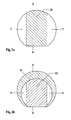
- the reference mark 6 is preferably arranged symmetrically with respect to the axis of one direction of movement, whereby the width of the reference mark projected in the direction of movement on the surface of the wafer 3 is an unauthorized zone 22, as in FIG Fig. 2a shaded, defined.
- the reference mark 6 could also be arranged asymmetrically with respect to this one direction of movement on the holder 10 of the transport device, but this would then lead to more complicated areas forming the unauthorized zone 22, because in this case the projections of two superimposed directions of movement would have to be taken into account.
- the wafer 3 is preferred with its reference mark 6, stored on the holder, that the reference mark 6 is directed against the rotation center 20 and in the further preferred symmetrical to Axis of the radial transport direction of the transport arm 21 is stored, as in Fig. 1b is shown schematically.
- Fig. 1b illustrated example then arise, as in Fig. 2a 3, 7, 22 on the wafer surface, which are defined by the reference mark 6 of the wafer 3 and the one radial direction of movement by the projection of the reference mark 6 representing an illicit hatched zone 22 extending from the reference mark 6 to the opposite peripheral edge of the wafer 3 is enough.
- the resulting laterally to the unauthorized zone 22 two segment-like free zones 7 thus have exclusively edge regions which lie on a circular line.
- the transport device 2, 20, 21 with the wafer 3 deposited thereon is positioned and guided relative to the sensor 1 arranged at a predetermined position such that only the two detection points 4, 5 at the wafer periphery of the so-called free zones 7 are detected when the wafer edge is detected be evaluated for the position detection.
- the tolerance bands of the inaccuracy of the transport device itself and the inaccuracy of the wafer deposit on the Bracket 10 are advantageously taken into account in determining the size of the surface of these free zones 7, for example, by superimposing the associated surfaces, which is not shown in the figures.
- the sensor 1 for the detection of the two detection points 4, 5 at the wafer edge is advantageously arranged in the transport chamber in the inlet region in front of the process chamber.
- the vacuum processing system with the transport device can also be designed universally for the processing of wafers 3 with different diameters.
- the largest wafer 3 to be processed and the smallest wafer 8 to be processed are projected onto one another and aligned with the two reference marks 6, as shown in FIG Fig. 2b is shown.
- the resulting free zone for the arrangement of the permissible measuring positions then results from the formed free zones 9 of the so-called overlapping zone, which is determined by the smallest wafer 8 to be processed.
- the wafer holder 10 should also, as already mentioned, below the forbidden zone 22 be arranged. In order to achieve a high measurement accuracy, it makes sense to choose the measuring points far apart, but this distance can not be greater than the wafer diameter.
- the precise evaluation option by the present positioning method now also allows to determine different operating conditions in the vacuum process system and in particular in the process chamber.
- very specific processes can be assigned and determined and, in addition, trend analyzes can be carried out.
- the safe operation of such a process plant can thereby be significantly increased. For example, corrective measures can be taken in good time, ensuring that the quality of production is maintained over a longer production period and, on the other hand, can be identified in good time if preventive maintenance becomes necessary before rejects are produced or even damage to the process plant.
- the desired position 12 of the wafer 3 is regularly displaced by a similar amount of the displacement vector 11 and the magnitude of the vector is approximately of the same order of magnitude as in FIG Fig. 3a is shown in polar depiction, then it can be concluded that the wafer 3 at a certain part of the plant, for example in the process station, touches or touching and thereby a displacement of the wafer position occurs.
- the displacement length or the displacement of the displacement vector is approximately equal to the number the measured values or over time, as in Fig. 3b is shown schematically.
- Fig. 4a is shown another example in which several measurements of a displacement of the desired position of the wafer center 12 are shown in polar representation, wherein the displacement direction is approximately the same and is within a certain range of the vector angle 15, wherein the displacement path length is different.
- Fig. 4b It is shown that this shift length increases over the course of time and the number of measured values 24.
- This behavior is typical, for example, for the adhesion or partial bonding of the wafer 3 to a shield, as required in coating process stations.
- the growing in the coating material on shields or panels leads to a wafer, for example, by a kind of soldering it can adhere to it and this moves with the increasing growth of the layer farther away.
- the evaluation of the measurement results allows, for example, the time when plant operation must be interrupted to clean or replace the shielding.
- the timely recognition of this operating state allows, for example, the avoidance of production scrap.
- Measured values 24 are shown which statistically are distributed in all directions with different displacement lengths 11 of the wafer 3.
- the displacement lengths 11 are shown over time in FIG Fig. 5b show that the shift length increases with time. This is a typical problem with so-called electrostatic wafer supports occurs. The problem increases in the course of the operating time and the performance of the holding effect decreases. Also from this example, appropriate measures can be derived in time when exceeding a predetermined level. As the illustrated examples show, by simply measuring the displacement vector 11, ie both by measuring the vector direction as well as its length, with several measurements over time, the cause can be determined which trigger the erroneous processes. It can thus be targeted and precisely derived and taken the appropriate necessary corrective action.
Landscapes
- Container, Conveyance, Adherence, Positioning, Of Wafer (AREA)
- Mechanical Treatment Of Semiconductor (AREA)
- Apparatuses And Processes For Manufacturing Resistors (AREA)
- Position Fixing By Use Of Radio Waves (AREA)
Claims (19)
- Procédé de positionnement d'une plaquette (3) avec un repère de référence (6) dans une installation de traitement sous vide qui inclut une chambre de transport, contenant une dispositif de transport (2, 20, 21) pour déplacer la plaquette (3) dans un plan vers une chambre de traitement adjacente à cette chambre, ainsi qu'un capteur unique (1) qui est disposé à l'intérieur de la chambre de transport avant la chambre de traitement pour détecter la position de la plaquette (3) en détectant sur son arête un premier point de détection (4) et un deuxième point de détection (5), d'une manière telle que la vraie situation de la plaquette (3) est établie pour un diamètre connu de plaquette par évaluation électronique des deux points de détection mesurés (4, 5) et que le dispositif de transport (2, 20, 21) oriente la plaquette (3) selon une position de consigne souhaitée, caractérisé en ce que la plaquette (3) est déposée sur le dispositif de transport (2, 20, 21) en étant ajustée dans une position prédéfinie en référence à son repère de référence (6) et que la projection du repère de référence (6) selon une direction de déplacement détermine une zone interdite (22) sur la plaquette (3), et que la région restante de la plaquette (3) définit de cette manière une zone libre, le capteur (1) étant disposé dans la chambre de transport d'une manière telle que la zone interdite (22) n'est certainement pas balayée et que le capteur (1) ne peut donc détecter que la région circulaire de l'arête de plaquette et non des parties du repère de référence (6).
- Procédé selon la revendication 1, caractérisé en ce que le positionnement est une manoeuvre de centrage de la plaquette pour ajuster le centre (12) de la plaquette sur la position de consigne souhaitée prédéfinie.
- Procédé selon la revendication 1 ou 2, caractérisé en ce que des mesures sont d'abord effectuées sur une première plaquette (3), et que des corrections sont apportées à une position de consigne pour d'autres plaquettes lors d'autres étapes de transport suivantes.
- Procédé selon l'une quelconque des revendications précédentes, caractérisé en ce que des erreurs de déport en translation sont corrigées.
- Procédé selon l'une quelconque des revendications précédentes, caractérisé en ce que le dispositif de transport exécute un déplacement de rotation autour d'un centre de rotation (20) et un déplacement radial vers ce centre ou en direction opposée afin de transporter une plaquette (3) vers une chambre de traitement et / ou une chambre de sas et / ou de l'y positionner.
- Procédé selon la revendication 5, caractérisé en ce que la configuration de l'installation de traitement sous vide est en grappe.
- Procédé selon l'une quelconque des revendications précédentes, caractérisé en ce que seuls deux points de détection (4, 5) sont détectés sur l'arête de la plaquette pour chaque plaquette (3) à mesurer.
- Procédé selon l'une quelconque des revendications précédentes, caractérisé en ce que la plaquette (3) est guidée avec son arête vers le capteur (1) pour la détection des points de détection (4, 5), au moyen d'un déplacement de rotation et / ou d'un déplacement linéaire dans le plan de transport.
- Procédé selon l'une quelconque des revendications précédentes, caractérisé en ce que les situations des points de détection (4, 5) sont choisies à distance l'une de l'autre, mais à une distance inférieure au diamètre de la plaquette à mesurer.
- Procédé selon l'une quelconque des revendications précédentes, caractérisé en ce que la bride de support de plaquette est formée d'une manière telle qu'elle ne gêne pas le déroulement des mesures et est positionnée de préférence au dessous de la zone interdite (22).
- Procédé selon l'une quelconque des revendications précédentes, caractérisé en ce que chaque plaquette (3) est déposée sur la bride de support du dispositif de transport (2, 20, 21) d'une manière telle que le repère de référence (6) est toujours ajusté de la même manière, qui est de préférence telle que le repère de référence (6) est ajusté pour faire face au centre de rotation (20), en vue selon la direction du déplacement linéaire radial (21).
- Procédé selon l'une quelconque des revendications précédentes, caractérisé en ce que les bandes de tolérance de la précision de positionnement du dispositif de transport (2, 20, 21) sont intégrées dans le calcul de la spécification de la zone interdite (22).
- Procédé selon l'une quelconque des revendications précédentes, caractérisé en ce qu'il prend en compte diverses dimensions de plaquettes qui établissent, en partant de la même situation de leurs repères de référence (6), une zone de recouvrement (9) qui représente la zone libre (7).
- Procédé selon l'une quelconque des revendications précédentes, caractérisé en ce que les écarts mesurés par rapport à la position de consigne de la plaquette (3) sont détectés et mémorisés de préférence pour chaque plaquette (3) afin de détecter l'état du système pour déduire des dispositions de correction.
- Procédé selon l'une quelconque des revendications précédentes, caractérisé en ce que la plaquette (3) est d'abord élaborée dans la chambre de traitement et est ensuite transportée hors de la chambre de traitement jusque dans la chambre de transport et y est ensuite mesurée par le capteur unique (1), et les valeurs de mesures sont converties par des moyens électroniques et des dispositions de correction correspondantes sont prises au cours de l'une des étapes suivantes du processus lorsqu'une valeur prédéfinie a été atteinte et / ou dépassée.
- Procédé selon la revendication 15, caractérisé en ce que plusieurs étapes de mesures sont converties et une tendance vers un type d'erreurs est établie, et des dispositions sont ensuite définies pour le mode opératoire ultérieur de l'installation de traitement sous vide, en particulier pour la commande du dispositif de transport (2, 20, 21).
- Procédé selon la revendication 16, caractérisé en ce que l'analyse de tendance détecte, au moyen de la plaquette (3), un contact de plaquette (3) dû à un réglage erroné du dispositif de transport.
- Procédé selon la revendication 16, caractérisé en ce que l'analyse de tendance détecte le glissement local de la plaquette (3) sur la bride de support (10) du dispositif de transport, résultant de croissances de couches sur des parties masquées.
- Procédé selon la revendication 16, caractérisé en ce que l'analyse de tendance détecte la perte d'efficacité de la force de maintien d'une bride de support électrostatique au cours du temps de fonctionnement.
Applications Claiming Priority (2)
| Application Number | Priority Date | Filing Date | Title |
|---|---|---|---|
| CH3092005 | 2005-02-22 | ||
| PCT/CH2006/000015 WO2006089435A1 (fr) | 2005-02-22 | 2006-01-09 | Procede de positionnement d'une plaquette |
Publications (2)
| Publication Number | Publication Date |
|---|---|
| EP1856730A1 EP1856730A1 (fr) | 2007-11-21 |
| EP1856730B1 true EP1856730B1 (fr) | 2010-12-29 |
Family
ID=34974747
Family Applications (1)
| Application Number | Title | Priority Date | Filing Date |
|---|---|---|---|
| EP06700022A Expired - Lifetime EP1856730B1 (fr) | 2005-02-22 | 2006-01-09 | Procede de positionnement d'une plaquette |
Country Status (9)
| Country | Link |
|---|---|
| US (1) | US7706908B2 (fr) |
| EP (1) | EP1856730B1 (fr) |
| JP (1) | JP2008530804A (fr) |
| KR (1) | KR101312789B1 (fr) |
| CN (1) | CN100524684C (fr) |
| AT (1) | ATE493757T1 (fr) |
| DE (1) | DE502006008604D1 (fr) |
| TW (1) | TWI375293B (fr) |
| WO (1) | WO2006089435A1 (fr) |
Families Citing this family (19)
| Publication number | Priority date | Publication date | Assignee | Title |
|---|---|---|---|---|
| JP5064835B2 (ja) * | 2007-02-28 | 2012-10-31 | 株式会社アルバック | 基板搬送装置 |
| JP2010239060A (ja) * | 2009-03-31 | 2010-10-21 | Tokyo Electron Ltd | オリエンテーションフラット指定方法、オリエンテーションフラット検出装置及びオリエンテーションフラット指定用プログラム |
| US9252037B2 (en) | 2010-12-29 | 2016-02-02 | Oerlikon Advanced Technologies Ag | Vacuum treatment apparatus and a method for manufacturing |
| TWI514089B (zh) * | 2011-04-28 | 2015-12-21 | 瑪波微影Ip公司 | 在微影系統中用於轉移基板的設備 |
| CN104718607B (zh) | 2012-08-31 | 2017-10-03 | 联达科技设备私人有限公司 | 用于自动校正膜片架上的晶圆的旋转错位的系统和方法 |
| CN103531509A (zh) * | 2013-09-26 | 2014-01-22 | 苏州经贸职业技术学院 | 一种工作台上精确定位圆心的方法 |
| CN104078402B (zh) * | 2014-06-30 | 2017-01-18 | 武汉新芯集成电路制造有限公司 | 一种机械手臂位置调整的辅助装置 |
| CN105632971B (zh) * | 2014-11-26 | 2019-06-25 | 上海微电子装备(集团)股份有限公司 | 一种硅片处理装置及方法 |
| CN106158715B (zh) | 2015-04-24 | 2021-04-02 | 上海微电子装备(集团)股份有限公司 | 用于晶圆的预对准装置及方法 |
| CN114758975A (zh) * | 2015-07-13 | 2022-07-15 | 博鲁可斯自动化美国有限责任公司 | 在传输中自动晶圆定中方法及设备 |
| US10068323B2 (en) * | 2016-04-10 | 2018-09-04 | Kla-Tencor Corporation | Aware system, method and computer program product for detecting overlay-related defects in multi-patterned fabricated devices |
| CN108074830B (zh) * | 2016-11-18 | 2020-08-11 | 沈阳芯源微电子设备股份有限公司 | 一种晶圆位置检测装置及其检测方法 |
| JP7292948B2 (ja) * | 2019-04-24 | 2023-06-19 | キヤノン株式会社 | 基板処理装置および基板処理方法 |
| CN113129368B (zh) * | 2020-01-15 | 2023-03-21 | 惠州市成泰自动化科技有限公司 | Pcb板方向的识别方法 |
| JP7579072B2 (ja) * | 2020-06-29 | 2024-11-07 | キヤノン株式会社 | 搬送装置、基板処理装置、および物品製造方法 |
| CN112103233B (zh) * | 2020-09-25 | 2023-08-22 | 广东先导微电子科技有限公司 | 确定晶片掰片位置的方法 |
| CN115479569A (zh) * | 2021-06-16 | 2022-12-16 | 盛美半导体设备(上海)股份有限公司 | 偏差测量装置 |
| CN113838791A (zh) * | 2021-08-30 | 2021-12-24 | 威科赛乐微电子股份有限公司 | 晶片取片、圆心定位装置、方法、系统及可读存储介质 |
| CN114823419B (zh) * | 2022-04-02 | 2022-11-22 | 法诺信息产业有限公司 | 一种具有高适配性的半导体芯片智能制造系统 |
Family Cites Families (20)
| Publication number | Priority date | Publication date | Assignee | Title |
|---|---|---|---|---|
| US5126028A (en) * | 1989-04-17 | 1992-06-30 | Materials Research Corporation | Sputter coating process control method and apparatus |
| JP2949528B2 (ja) * | 1991-03-13 | 1999-09-13 | 東京エレクトロン株式会社 | ウエハの中心位置検出方法及びその装置 |
| US5586585A (en) * | 1995-02-27 | 1996-12-24 | Asyst Technologies, Inc. | Direct loadlock interface |
| US5855681A (en) * | 1996-11-18 | 1999-01-05 | Applied Materials, Inc. | Ultra high throughput wafer vacuum processing system |
| US6082950A (en) * | 1996-11-18 | 2000-07-04 | Applied Materials, Inc. | Front end wafer staging with wafer cassette turntables and on-the-fly wafer center finding |
| JPH10223732A (ja) * | 1996-12-02 | 1998-08-21 | Toyota Autom Loom Works Ltd | 位置ずれ検出装置およびその方法 |
| EP1063186A1 (fr) * | 1997-12-03 | 2000-12-27 | Nikon Corporation | Dispositif et procede de transfert de substrats |
| GB2349204B (en) * | 1999-04-19 | 2004-03-03 | Applied Materials Inc | A method of detecting the position of a wafer |
| US6342705B1 (en) * | 1999-09-10 | 2002-01-29 | Chapman Instruments | System for locating and measuring an index mark on an edge of a wafer |
| JP2001127044A (ja) * | 1999-10-29 | 2001-05-11 | Hitachi Ltd | 真空処理装置および真空処理システム |
| JP2002043394A (ja) * | 2000-07-19 | 2002-02-08 | Tokyo Electron Ltd | 位置ずれ検出装置及び処理システム |
| US7457680B2 (en) * | 2000-12-27 | 2008-11-25 | Tokyo Electron Limited | Conveyance method for transporting objects |
| JP2003065711A (ja) * | 2001-07-31 | 2003-03-05 | Applied Materials Inc | 基板の検出装置及び半導体製造装置 |
| JP2003110004A (ja) * | 2001-09-28 | 2003-04-11 | Assist Japan Kk | ウェハ搬送における位置補正方法 |
| US6900877B2 (en) * | 2002-06-12 | 2005-05-31 | Asm American, Inc. | Semiconductor wafer position shift measurement and correction |
| US6760976B1 (en) * | 2003-01-15 | 2004-07-13 | Novellus Systems, Inc. | Method for active wafer centering using a single sensor |
| JP4137711B2 (ja) * | 2003-06-16 | 2008-08-20 | 東京エレクトロン株式会社 | 基板処理装置及び基板搬送手段の位置合わせ方法 |
| US7319920B2 (en) * | 2003-11-10 | 2008-01-15 | Applied Materials, Inc. | Method and apparatus for self-calibration of a substrate handling robot |
| FI117651B (fi) * | 2005-01-04 | 2006-12-29 | Metso Paper Inc | Menetelmä ja sovitelma ympyrämäisen objektin sijainnin mittaamiseksi |
| CN100358097C (zh) * | 2005-08-05 | 2007-12-26 | 中微半导体设备(上海)有限公司 | 半导体工艺处理系统及其处理方法 |
-
2006
- 2006-01-09 US US11/815,741 patent/US7706908B2/en not_active Expired - Fee Related
- 2006-01-09 EP EP06700022A patent/EP1856730B1/fr not_active Expired - Lifetime
- 2006-01-09 WO PCT/CH2006/000015 patent/WO2006089435A1/fr not_active Ceased
- 2006-01-09 CN CNB2006800057728A patent/CN100524684C/zh not_active Expired - Fee Related
- 2006-01-09 JP JP2007555434A patent/JP2008530804A/ja active Pending
- 2006-01-09 AT AT06700022T patent/ATE493757T1/de not_active IP Right Cessation
- 2006-01-09 KR KR1020077016399A patent/KR101312789B1/ko not_active Expired - Fee Related
- 2006-01-09 DE DE502006008604T patent/DE502006008604D1/de not_active Expired - Lifetime
- 2006-01-23 TW TW095102452A patent/TWI375293B/zh not_active IP Right Cessation
Also Published As
| Publication number | Publication date |
|---|---|
| EP1856730A1 (fr) | 2007-11-21 |
| JP2008530804A (ja) | 2008-08-07 |
| ATE493757T1 (de) | 2011-01-15 |
| TW200631122A (en) | 2006-09-01 |
| TWI375293B (en) | 2012-10-21 |
| US7706908B2 (en) | 2010-04-27 |
| CN101128928A (zh) | 2008-02-20 |
| KR101312789B1 (ko) | 2013-09-27 |
| WO2006089435A1 (fr) | 2006-08-31 |
| CN100524684C (zh) | 2009-08-05 |
| KR20070114117A (ko) | 2007-11-29 |
| DE502006008604D1 (de) | 2011-02-10 |
| US20080152474A1 (en) | 2008-06-26 |
Similar Documents
| Publication | Publication Date | Title |
|---|---|---|
| EP1856730B1 (fr) | Procede de positionnement d'une plaquette | |
| DE3715601C2 (de) | Ofensystem zur Erhitzung und/oder Behandlung von Wafern | |
| DE60035164T2 (de) | Verfahren und Gerät zur Entscheidung einer Substratsverschiebung mit Optimierungsmethoden | |
| DE69329269T2 (de) | System und Verfahren für automatische Positionierung eines Substrats in einem Prozessraum | |
| DE3402664C2 (de) | Verfahren zur Behandlung und/oder Handhabung eines Wafers, Einrichtung zur Durchführung des Verfahrens sowie Verwendung des Verfahrens in Wafer-Bearbeitungsstationen | |
| DE3752234T2 (de) | Transfersystem für Halbleiterscheibe | |
| DE3889473T2 (de) | Vorrichtung zum Handhaben eines Wafers. | |
| DE69422700T2 (de) | Waferhalteplatte und hebevorrichtung | |
| DE69706983T2 (de) | Anlage zum behandeln von substraten mit einem plasmastrahl | |
| DE19957758C2 (de) | Vorrichtung und Verfahren zum Ausrichten von scheibenförmigen Substraten | |
| EP1826812A1 (fr) | Dispositif et procédé destinés à la réception et/ou le transport de substrats | |
| EP1952437B1 (fr) | Dispositif de transport pour pièces en forme de disque | |
| EP0886302A2 (fr) | Réacteur à dispositif de protection pour le traitement de plaques semiconductrices | |
| DE10121044B4 (de) | Anordnung zur Waferinspektion | |
| DE3242855A1 (de) | Verfahren und vorrichtung zur konturierung der dicke von aufgespruehten schichten | |
| DE102020119873A1 (de) | Verfahren zum Erkennen fehlerhafter oder fehlerhaft in einem CVD-Reaktor eingesetzte Substrate | |
| DE102011120565B4 (de) | Vorrichtung und Verfahren zum Vermessen eines scheibenförmigen Substrats | |
| DE3745134C2 (de) | Verfahren und Einrichtung zur Übertragung eines Wafers von einer Quelle zu einem Zielort | |
| DE102013106788A1 (de) | Vakuumkammerdurchführung, Vakuumbehandlungsanlage mit Vakuumkammerdurchführung und Verwendung einer Vakuumkammerdurchführung | |
| DE102006015089A1 (de) | System und Verfahren zur Scheibenhandhabung in Halbleiterprozessanlagen | |
| DE102011076742B4 (de) | Verfahren zum Ablegen einer Halbleiterscheibe auf einem Suszeptor mit einer vorgegebenen Winkelorientierung | |
| DE69500796T2 (de) | Ladungsvorrichtung für Halbleiter-Plättchen | |
| DE3822597A1 (de) | Justiervorrichtung und verfahren zum justieren eines roboterarms zum einsatz in automatisierten produktionsbereichen insbesondere in der halbleitertechnik | |
| DE3822598C2 (de) | Justieranordnung und Verfahren zum Justieren einer Greifvorrichtung eines Roboterarms zum Handhaben einer Halbleiterscheibe | |
| EP1442839B1 (fr) | Procédé et dispositif pour manipuler des plaquettes |
Legal Events
| Date | Code | Title | Description |
|---|---|---|---|
| PUAI | Public reference made under article 153(3) epc to a published international application that has entered the european phase |
Free format text: ORIGINAL CODE: 0009012 |
|
| 17P | Request for examination filed |
Effective date: 20070924 |
|
| AK | Designated contracting states |
Kind code of ref document: A1 Designated state(s): AT BE BG CH CY CZ DE DK EE ES FI FR GB GR HU IE IS IT LI LT LU LV MC NL PL PT RO SE SI SK TR |
|
| RIN1 | Information on inventor provided before grant (corrected) |
Inventor name: CHRIST, HOLGER Inventor name: SCHMUCKI, RUEDI Inventor name: SCHOLTE VAN MAST, BART |
|
| DAX | Request for extension of the european patent (deleted) | ||
| GRAP | Despatch of communication of intention to grant a patent |
Free format text: ORIGINAL CODE: EPIDOSNIGR1 |
|
| GRAS | Grant fee paid |
Free format text: ORIGINAL CODE: EPIDOSNIGR3 |
|
| GRAA | (expected) grant |
Free format text: ORIGINAL CODE: 0009210 |
|
| AK | Designated contracting states |
Kind code of ref document: B1 Designated state(s): AT BE BG CH CY CZ DE DK EE ES FI FR GB GR HU IE IS IT LI LT LU LV MC NL PL PT RO SE SI SK TR |
|
| REG | Reference to a national code |
Ref country code: GB Ref legal event code: FG4D Free format text: NOT ENGLISH |
|
| REG | Reference to a national code |
Ref country code: CH Ref legal event code: EP |
|
| REG | Reference to a national code |
Ref country code: IE Ref legal event code: FG4D Free format text: LANGUAGE OF EP DOCUMENT: GERMAN |
|
| REF | Corresponds to: |
Ref document number: 502006008604 Country of ref document: DE Date of ref document: 20110210 Kind code of ref document: P |
|
| REG | Reference to a national code |
Ref country code: DE Ref legal event code: R096 Ref document number: 502006008604 Country of ref document: DE Effective date: 20110210 |
|
| REG | Reference to a national code |
Ref country code: NL Ref legal event code: VDEP Effective date: 20101229 |
|
| PG25 | Lapsed in a contracting state [announced via postgrant information from national office to epo] |
Ref country code: LT Free format text: LAPSE BECAUSE OF FAILURE TO SUBMIT A TRANSLATION OF THE DESCRIPTION OR TO PAY THE FEE WITHIN THE PRESCRIBED TIME-LIMIT Effective date: 20101229 |
|
| LTIE | Lt: invalidation of european patent or patent extension |
Effective date: 20101229 |
|
| PG25 | Lapsed in a contracting state [announced via postgrant information from national office to epo] |
Ref country code: SE Free format text: LAPSE BECAUSE OF FAILURE TO SUBMIT A TRANSLATION OF THE DESCRIPTION OR TO PAY THE FEE WITHIN THE PRESCRIBED TIME-LIMIT Effective date: 20101229 Ref country code: LV Free format text: LAPSE BECAUSE OF FAILURE TO SUBMIT A TRANSLATION OF THE DESCRIPTION OR TO PAY THE FEE WITHIN THE PRESCRIBED TIME-LIMIT Effective date: 20101229 Ref country code: CY Free format text: LAPSE BECAUSE OF FAILURE TO SUBMIT A TRANSLATION OF THE DESCRIPTION OR TO PAY THE FEE WITHIN THE PRESCRIBED TIME-LIMIT Effective date: 20101229 Ref country code: FI Free format text: LAPSE BECAUSE OF FAILURE TO SUBMIT A TRANSLATION OF THE DESCRIPTION OR TO PAY THE FEE WITHIN THE PRESCRIBED TIME-LIMIT Effective date: 20101229 Ref country code: BG Free format text: LAPSE BECAUSE OF FAILURE TO SUBMIT A TRANSLATION OF THE DESCRIPTION OR TO PAY THE FEE WITHIN THE PRESCRIBED TIME-LIMIT Effective date: 20110329 Ref country code: SI Free format text: LAPSE BECAUSE OF FAILURE TO SUBMIT A TRANSLATION OF THE DESCRIPTION OR TO PAY THE FEE WITHIN THE PRESCRIBED TIME-LIMIT Effective date: 20101229 |
|
| PG25 | Lapsed in a contracting state [announced via postgrant information from national office to epo] |
Ref country code: IS Free format text: LAPSE BECAUSE OF FAILURE TO SUBMIT A TRANSLATION OF THE DESCRIPTION OR TO PAY THE FEE WITHIN THE PRESCRIBED TIME-LIMIT Effective date: 20110429 Ref country code: PT Free format text: LAPSE BECAUSE OF FAILURE TO SUBMIT A TRANSLATION OF THE DESCRIPTION OR TO PAY THE FEE WITHIN THE PRESCRIBED TIME-LIMIT Effective date: 20110429 Ref country code: CZ Free format text: LAPSE BECAUSE OF FAILURE TO SUBMIT A TRANSLATION OF THE DESCRIPTION OR TO PAY THE FEE WITHIN THE PRESCRIBED TIME-LIMIT Effective date: 20101229 Ref country code: ES Free format text: LAPSE BECAUSE OF FAILURE TO SUBMIT A TRANSLATION OF THE DESCRIPTION OR TO PAY THE FEE WITHIN THE PRESCRIBED TIME-LIMIT Effective date: 20110409 Ref country code: EE Free format text: LAPSE BECAUSE OF FAILURE TO SUBMIT A TRANSLATION OF THE DESCRIPTION OR TO PAY THE FEE WITHIN THE PRESCRIBED TIME-LIMIT Effective date: 20101229 Ref country code: GR Free format text: LAPSE BECAUSE OF FAILURE TO SUBMIT A TRANSLATION OF THE DESCRIPTION OR TO PAY THE FEE WITHIN THE PRESCRIBED TIME-LIMIT Effective date: 20110330 |
|
| BERE | Be: lapsed |
Owner name: OC OERLIKON BALZERS AG Effective date: 20110131 |
|
| PG25 | Lapsed in a contracting state [announced via postgrant information from national office to epo] |
Ref country code: NL Free format text: LAPSE BECAUSE OF FAILURE TO SUBMIT A TRANSLATION OF THE DESCRIPTION OR TO PAY THE FEE WITHIN THE PRESCRIBED TIME-LIMIT Effective date: 20101229 Ref country code: PL Free format text: LAPSE BECAUSE OF FAILURE TO SUBMIT A TRANSLATION OF THE DESCRIPTION OR TO PAY THE FEE WITHIN THE PRESCRIBED TIME-LIMIT Effective date: 20101229 Ref country code: RO Free format text: LAPSE BECAUSE OF FAILURE TO SUBMIT A TRANSLATION OF THE DESCRIPTION OR TO PAY THE FEE WITHIN THE PRESCRIBED TIME-LIMIT Effective date: 20101229 Ref country code: SK Free format text: LAPSE BECAUSE OF FAILURE TO SUBMIT A TRANSLATION OF THE DESCRIPTION OR TO PAY THE FEE WITHIN THE PRESCRIBED TIME-LIMIT Effective date: 20101229 Ref country code: MC Free format text: LAPSE BECAUSE OF NON-PAYMENT OF DUE FEES Effective date: 20110131 |
|
| PG25 | Lapsed in a contracting state [announced via postgrant information from national office to epo] |
Ref country code: DK Free format text: LAPSE BECAUSE OF FAILURE TO SUBMIT A TRANSLATION OF THE DESCRIPTION OR TO PAY THE FEE WITHIN THE PRESCRIBED TIME-LIMIT Effective date: 20101229 |
|
| PLBE | No opposition filed within time limit |
Free format text: ORIGINAL CODE: 0009261 |
|
| STAA | Information on the status of an ep patent application or granted ep patent |
Free format text: STATUS: NO OPPOSITION FILED WITHIN TIME LIMIT |
|
| PG25 | Lapsed in a contracting state [announced via postgrant information from national office to epo] |
Ref country code: BE Free format text: LAPSE BECAUSE OF NON-PAYMENT OF DUE FEES Effective date: 20110131 |
|
| 26N | No opposition filed |
Effective date: 20110930 |
|
| REG | Reference to a national code |
Ref country code: DE Ref legal event code: R097 Ref document number: 502006008604 Country of ref document: DE Effective date: 20110930 |
|
| REG | Reference to a national code |
Ref country code: AT Ref legal event code: MM01 Ref document number: 493757 Country of ref document: AT Kind code of ref document: T Effective date: 20110109 |
|
| PG25 | Lapsed in a contracting state [announced via postgrant information from national office to epo] |
Ref country code: AT Free format text: LAPSE BECAUSE OF NON-PAYMENT OF DUE FEES Effective date: 20110109 |
|
| PG25 | Lapsed in a contracting state [announced via postgrant information from national office to epo] |
Ref country code: LU Free format text: LAPSE BECAUSE OF NON-PAYMENT OF DUE FEES Effective date: 20110109 |
|
| PG25 | Lapsed in a contracting state [announced via postgrant information from national office to epo] |
Ref country code: TR Free format text: LAPSE BECAUSE OF FAILURE TO SUBMIT A TRANSLATION OF THE DESCRIPTION OR TO PAY THE FEE WITHIN THE PRESCRIBED TIME-LIMIT Effective date: 20101229 |
|
| PG25 | Lapsed in a contracting state [announced via postgrant information from national office to epo] |
Ref country code: HU Free format text: LAPSE BECAUSE OF FAILURE TO SUBMIT A TRANSLATION OF THE DESCRIPTION OR TO PAY THE FEE WITHIN THE PRESCRIBED TIME-LIMIT Effective date: 20101229 |
|
| REG | Reference to a national code |
Ref country code: CH Ref legal event code: PFA Owner name: OERLIKON ADVANCED TECHNOLOGIES AG, LI Free format text: FORMER OWNER: OC OERLIKON BALZERS AG, LI |
|
| PGFP | Annual fee paid to national office [announced via postgrant information from national office to epo] |
Ref country code: IT Payment date: 20140113 Year of fee payment: 9 |
|
| REG | Reference to a national code |
Ref country code: FR Ref legal event code: TP Owner name: OERLIKON ADVANCED TECHNOLOGIES AG, LI Effective date: 20140627 |
|
| REG | Reference to a national code |
Ref country code: GB Ref legal event code: 732E Free format text: REGISTERED BETWEEN 20140717 AND 20140723 |
|
| PGFP | Annual fee paid to national office [announced via postgrant information from national office to epo] |
Ref country code: CH Payment date: 20140424 Year of fee payment: 9 |
|
| REG | Reference to a national code |
Ref country code: DE Ref legal event code: R081 Ref document number: 502006008604 Country of ref document: DE Owner name: OERLIKON ADVANCED TECHNOLOGIES AG, LI Free format text: FORMER OWNER: OC OERLIKON BALZERS AG, BALZERS, LI Effective date: 20141216 |
|
| PGFP | Annual fee paid to national office [announced via postgrant information from national office to epo] |
Ref country code: IE Payment date: 20150112 Year of fee payment: 10 |
|
| REG | Reference to a national code |
Ref country code: CH Ref legal event code: PL |
|
| PG25 | Lapsed in a contracting state [announced via postgrant information from national office to epo] |
Ref country code: LI Free format text: LAPSE BECAUSE OF NON-PAYMENT OF DUE FEES Effective date: 20150131 Ref country code: CH Free format text: LAPSE BECAUSE OF NON-PAYMENT OF DUE FEES Effective date: 20150131 |
|
| REG | Reference to a national code |
Ref country code: FR Ref legal event code: PLFP Year of fee payment: 11 |
|
| PG25 | Lapsed in a contracting state [announced via postgrant information from national office to epo] |
Ref country code: IT Free format text: LAPSE BECAUSE OF NON-PAYMENT OF DUE FEES Effective date: 20150109 |
|
| REG | Reference to a national code |
Ref country code: IE Ref legal event code: MM4A |
|
| REG | Reference to a national code |
Ref country code: FR Ref legal event code: PLFP Year of fee payment: 12 |
|
| PG25 | Lapsed in a contracting state [announced via postgrant information from national office to epo] |
Ref country code: IE Free format text: LAPSE BECAUSE OF NON-PAYMENT OF DUE FEES Effective date: 20160109 |
|
| PGFP | Annual fee paid to national office [announced via postgrant information from national office to epo] |
Ref country code: FR Payment date: 20161215 Year of fee payment: 12 |
|
| PGFP | Annual fee paid to national office [announced via postgrant information from national office to epo] |
Ref country code: DE Payment date: 20170104 Year of fee payment: 12 |
|
| PGFP | Annual fee paid to national office [announced via postgrant information from national office to epo] |
Ref country code: GB Payment date: 20170104 Year of fee payment: 12 |
|
| REG | Reference to a national code |
Ref country code: DE Ref legal event code: R119 Ref document number: 502006008604 Country of ref document: DE |
|
| GBPC | Gb: european patent ceased through non-payment of renewal fee |
Effective date: 20180109 |
|
| PG25 | Lapsed in a contracting state [announced via postgrant information from national office to epo] |
Ref country code: FR Free format text: LAPSE BECAUSE OF NON-PAYMENT OF DUE FEES Effective date: 20180131 Ref country code: DE Free format text: LAPSE BECAUSE OF NON-PAYMENT OF DUE FEES Effective date: 20180801 |
|
| REG | Reference to a national code |
Ref country code: FR Ref legal event code: ST Effective date: 20180928 |
|
| PG25 | Lapsed in a contracting state [announced via postgrant information from national office to epo] |
Ref country code: GB Free format text: LAPSE BECAUSE OF NON-PAYMENT OF DUE FEES Effective date: 20180109 |