EP1865649A1 - Récupération d'horloge et de données utilisant le surèchantillonage ainsi que le suivi de données. - Google Patents
Récupération d'horloge et de données utilisant le surèchantillonage ainsi que le suivi de données. Download PDFInfo
- Publication number
- EP1865649A1 EP1865649A1 EP06011597A EP06011597A EP1865649A1 EP 1865649 A1 EP1865649 A1 EP 1865649A1 EP 06011597 A EP06011597 A EP 06011597A EP 06011597 A EP06011597 A EP 06011597A EP 1865649 A1 EP1865649 A1 EP 1865649A1
- Authority
- EP
- European Patent Office
- Prior art keywords
- clock
- data recovery
- counter
- stream
- state
- Prior art date
- Legal status (The legal status is an assumption and is not a legal conclusion. Google has not performed a legal analysis and makes no representation as to the accuracy of the status listed.)
- Withdrawn
Links
- 238000011084 recovery Methods 0.000 title claims abstract description 80
- 230000007704 transition Effects 0.000 claims abstract description 59
- 238000000034 method Methods 0.000 claims description 96
- 239000013598 vector Substances 0.000 claims description 31
- 235000015047 pilsener Nutrition 0.000 claims description 17
- 238000001514 detection method Methods 0.000 claims description 12
- 230000008859 change Effects 0.000 claims description 11
- 230000007935 neutral effect Effects 0.000 claims 1
- 238000010586 diagram Methods 0.000 description 8
- 238000005516 engineering process Methods 0.000 description 8
- 238000004891 communication Methods 0.000 description 5
- 230000009471 action Effects 0.000 description 4
- 230000005540 biological transmission Effects 0.000 description 2
- 230000000694 effects Effects 0.000 description 2
- 230000000630 rising effect Effects 0.000 description 2
- 238000005070 sampling Methods 0.000 description 2
- 238000000605 extraction Methods 0.000 description 1
- 230000006870 function Effects 0.000 description 1
- 230000008569 process Effects 0.000 description 1
- 230000011664 signaling Effects 0.000 description 1
Images


Classifications
-
- H—ELECTRICITY
- H04—ELECTRIC COMMUNICATION TECHNIQUE
- H04L—TRANSMISSION OF DIGITAL INFORMATION, e.g. TELEGRAPHIC COMMUNICATION
- H04L7/00—Arrangements for synchronising receiver with transmitter
- H04L7/02—Speed or phase control by the received code signals, the signals containing no special synchronisation information
- H04L7/033—Speed or phase control by the received code signals, the signals containing no special synchronisation information using the transitions of the received signal to control the phase of the synchronising-signal-generating means, e.g. using a phase-locked loop
- H04L7/0331—Speed or phase control by the received code signals, the signals containing no special synchronisation information using the transitions of the received signal to control the phase of the synchronising-signal-generating means, e.g. using a phase-locked loop with a digital phase-locked loop [PLL] processing binary samples, e.g. add/subtract logic for correction of receiver clock
-
- H—ELECTRICITY
- H04—ELECTRIC COMMUNICATION TECHNIQUE
- H04L—TRANSMISSION OF DIGITAL INFORMATION, e.g. TELEGRAPHIC COMMUNICATION
- H04L7/00—Arrangements for synchronising receiver with transmitter
- H04L7/02—Speed or phase control by the received code signals, the signals containing no special synchronisation information
- H04L7/033—Speed or phase control by the received code signals, the signals containing no special synchronisation information using the transitions of the received signal to control the phase of the synchronising-signal-generating means, e.g. using a phase-locked loop
- H04L7/0337—Selecting between two or more discretely delayed clocks or selecting between two or more discretely delayed received code signals
Definitions
- the present invention relates to a clock and data recovery method and corresponding device.
- the invention particularly, but not exclusively, relates to a clock and data recovery method for an ASIC chip designed for telecom/datacorn applications and the following description is made with reference to this field of application for convenience of explanation only.
- an ASIC (acronym from Application-Specific Integrated Circuit) is a chip designed for a particular application. It typically consists of a core logic, where the specific application is implemented, and an in/out interface, that connects the specific application to the overall system.
- An ASIC for telecom/datacom applications generally includes, as an input/output interface, a SERDES interface (serial-to-parallel/parallel-to-scrial interface). Its goal is to adapt high speed serial data rate of a data line to low speed parallel data rate of the chip core: Line data rate is linked to bandwidth requirements of communication systems and limited by technology. Core data rate is linked to the available technology (for instance, the CMOS technology presently used) in terms of both maximum operating frequencies and digital design tools.
- a SERDES interface serial-to-parallel/parallel-to-scrial interface
- an ASIC is required to be able to treat a high data rate as well as a low data rate through the very same SERDES interface.
- the low data rate is usually an integer sub-rate of the high data rate.
- timing control is one of the highest priorities in data transmission through ASICs since the reliability and the quality of a data link or generally of a communication line strongly depend on the timing control indeed.
- communication lines with a clock signal transmitted therethrough have strong timing budget requirements, which become harder and harder to meet when the data rate increases; since the bit period becomes smaller and smaller.
- the most popular way to control timing is by embedding a clock signal into the transmitted data and recovering the timing information at the receiver side of the communication line by means of a clock and data recovery device (CDR in the following).
- CDR clock and data recovery device
- the CDR must recover the timing information based on the transitions of input data, under the assumption that the nominal bit period is constant, thus producing a recovered data signal as well as a recovered clock signal.
- a serial to parallel converter matches the line data rate and the core data rate.
- analog phase-locked loops have been used to implement CDR devices.
- an analog PLL can operate at high frequencies, it suffers from problems such as, for instance, the frequency drift during long sequences uf identical bits (also indicated as CID, Consecutive Identical Digits) and the difficult lock acquisition process (at the power on or after a loss of synchronization) .
- VHDL high level language
- Digital timing recovery in a serial connection line is typically done by a CDR device in two ways that are by tracking and by oversampling.
- a strong difference between tracking and oversampling CDRs is that the former solution recovers the clock while the latter recovers the data.
- the output of a tracking CDR is a data-clock pair with a known phase relationship, while the output of an oversampling CDR is typically a data signal.
- the technical problem underlying the present invention is that of providing a clock and data recovery method and corresponding device having structural and functional characteristics which allow to improve the scalability with different technologies and frequencies, in this way overcoming the limits which still affect the methods and devices realised according to the prior art.
- the solution idea underlying the present invention is that of providing a clock and data recovery method and corresponding device able to mix the tracking and oversampling features, in particular based on a serial-to-parallel converter that oversamples the input data and on a divider that can be controlled to track input data.
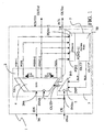
- the clock and data recovery device 1 comprises an oversampling portion 2 and a tracking portion 3, duly mixed in order to provide the desired recovery of the clock and data signals from a signal transmitted through a connection line. More particularly, an input data stream IDS is applied to a first input terminal IN of the clock and data recovery device 1, a recovered data signal RDATA being issued to a first output terminal OUTrd thereof.
- the clock and data recovery device 1 according to the invention also has a second input terminal INck receiving a reference clock signal CK and a second output terminal OUTrc issuing a recovered clock signal RCK.
- the oversampling portion 2 advantageously comprises a serial-to-parallel converter 4 in turn including a hold portion 4A and having a first input terminal IN4 connected to the first input terminal IN of the clock and data recovery device 1, thus receiving the input data stream IDS, and a second input terminal IN4ck connected to the second input terminal INck of the clock and data recovery device 1, thus receiving a reference clock CK, the reference clock CK being is N times faster than the input data stream IDS, where N is an even integer.
- the reference clock CK frequency is N*fbit [MHz].
- the serial-to-parallel converter 4 also has a plurality of parallel output terminals, PO[N], ..., PO[1], globally indicated as a parallel output PO[i], the first input bit of a current word of the input data stream IDS being at the output terminal PO[N] and the N-th input bit of the current word of the input data stream IDS being at the output terminal PO[1]. It is thus clear that N is also the width of the parallel output PO[i].
- serial-to-parallel converter 4 is also indicate as SIPO (Serial In Parallel Out).
- a central output terminal PO[N/2+1] is connected to the first output terminal OUTrd of the clock and data recovery device 1, wherein the recovered data signal RDATA is provided, having a rate equal to the data rate fbit.
- the serial-to-parallel converter 4 advantageously realises an oversampling of the input data stream IDS at a rate equal to N*fbit.
- serial-to-parallel converter 1 has a further output terminal PO[N+1] in correspondence of its hold portion 4A, wherein a last input bit of a previous word of the input data stream IDS is provided at the same time of the N input bits of the current input data stream IDS , as required when looking for transitions over N bits.
- the tracking portion 3 comprises a divider 5 having a first input terminal IN5ck connected to the second input terminal INck of the clock and data recovery device 1 and receiving the reference clock signal CK, as well as a second and third input terminals, IN5 and IN5*, connected to respective output terminals, OUT7 and OUT7*, of a detection and decision block 7, also included in the tracking portion 3.
- the divider 5 also has an output terminal OUT5 connected to the serial-to-parallel converter 4 as well as to the second output terminal OUTrc of the clock and data recovery device 1, wherein the recovered clock RCK is provided. More particularly, the recovered clock RCK has been obtained by the divider 5 and it is a divided signal having a rate which is equal to the data rate fbit.
- the detection and decision block 7 comprises a detection block or detector 7A, and a decision block 7B connected to each other, the detection block 7A having a plurality of parallel input terminals PI[N+1], ..., PI[1], globally indicated as a parallel input PI[i], connected to the parallel output PO[i] of the serial-to-parallel converter 4.
- the decision block 7B has the first and second output terminals, OUT7 and OUT7*, connected to the divider 5 and providing thereto a first driving signal SLIP and a second driving signal PILS, which change a dividing ratio of the divider 5 of + 1 and - 1, respectively.
- the clock and data recovery device 1 implements a clock and data recovery method which comprises essentially an oversampling and a tracking step, as explained in the following.
- the oversampling step is performed by the oversampling portion 2 using the serial-to-parallel converter 4 which receives the reference clock CK and produce a plurality of samples forming an oversampled stream of the input data stream IDS, in particular, at the parallel output PO[i] of the serial-to-parallel converter 4, being its length equal to a bit period of the input data stream IDS itself.
- Each parallel output terminal thus provides a sample of the input data stream IDS.
- the tracking step of the input data stream IDS is then performed by the tracking portion 3.
- Timing or clock information for the decision block 7B of the tracking portion 3 is obtained in terms of transitions between adjacent samples provided by the serial-to-parallel converter 4 of the oversampling portion 2 at its parallel output PO[i], such transitions being detected by the detection block 7A.
- the decision block 7B controls the divider 5 of the tracking portion 3, by changing its dividing ratio of ⁇ 1 (thanks to the SLIP/PILS driving signals), in order to move and keep a no transition area in the middle of the parallel output PO[i] (central output PO[N/2+1]), i.e, an area wherein no transitions between adjacent samples are found.
- the recovered data signal RDATA is thus obtained at the central output PO[N/2+1] of the serial-to-parallel converter 4 of the oversampling portion 2, while the recovered clock signal RCK is obtained at the output OUT5 of the divider 5 of the tracking portion 3. It has to be highlighted that the input data stream IDS is not actually serial-to-parallel converted by the clock and data recovery device 1 according to the invention.
- each parallel output terminal PO[1]...PO[N] covers 1/N UI (i.e. one sample) at the input data rate fbit or 1 UI at the oversampling rate N*fbit.
- Figure 2B shows how the input data stream IDS is analyzed in order to generate variables for the recovery algorithm.
- the logic values at adjacent parallel output terminals of the serial-to-parallel converter 4 are tested (for instance, through exclusive-or or XOR logic function).
- information from a central range of output terminals is used during both a first or SEARCH state and a second or TRACK state (Search Window SW), while information from the boundary terminals is used during the TRACK state only (in particular, by Track Vectors, as explained hereinafter).
- the Search Window has a programmable starting width; its current width can be narrowed down to 2 UI at the oversampling rate according to the recovery algorithm, i.e. according to the actual input data stream IDS.
- Track Vectors, VU and VD are used by the recovery algorithm to drive the signals SLIP and PILS in the proper way and have the very same length that is programmable.
- clock and data recovery method comprises the following states:
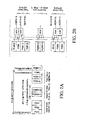
- Figure 3 represents a top level state diagram of the method according to the invention. At the power on, the working state of the method is the first or SEARCH state.
- the working state becomes the second or TRACK state when the current search window SW has no transition for N_LOCK times (N_LOCK being programmable). If the previous condition is not satisfied, then the working state does not change. Details about the SEARCH state are given later on.
- TRACK state a single transition which is found in the current search window SW changes the working state to the SEARCH state.
- the working state remains the TRACK state as far as no transition is found in the current search window SW. Details about the TRACK state are given later on.
- a single transition in the search window SW makes the state changing from the TRACK state to the SEARCH state.
- the state is the SEARCH state (command NOT(gotoT) in Figure 3].
- FIG. 4 A flow diagram of the clock and data recovery method in the first or SEARCH is shown in Figure 4.
- the clock and data recovery method in the SEARCH state comprises :
- the method comprises the following steps:
- the method further comprises a first assertion step S7 wherein a first state parameter LOCK is asserted and a first output condition TS (change of state) to the TRACK state is provided.
- the first counter SEARCH_CNT keeps count of how many times no transitions are found in the search window SW and it is set equal to 0 and reset when it reaches the first value N_LOCK, such value being equal to the number of times without transitions in order to assert the first state parameter LOCK and move from the search state to the track state (first output condition or change of state TS).
- the method further comprises the following steps:
- the method then return to the first verify step S4.
- the second counter SLIP_CNT keeps count of how many SLIP commands have been provided or scroll up decisions have been taken; it is set equal to 0, and reset when it reaches the value N-1 (i.e., after the whole parallel output PO[i] has been scrolled up), N being the number of parallel, output PO[i] of the serial-to-parallel converter 4 and the oversampling ratio (even number).
- the method comprises the following steps:
- the method further comprises a first reset step S13, wherein the second counter SLIP_CNT is set equal to 0 and the method goes back to the first verify step S4.
- the method comprises a second assertion step S 14 wherein the driving parameter NO_EYE is asserted.
- the initial width N-2*k0 of the search window SW is set by an initial value k0 of a k counter, being O ⁇ kO ⁇ N MIN_EYELAPE ⁇ /2 and the k counter reset when an output condition, corresponding to the first output condition TS and to the first assertion step S7 or the final assertion step S14, is reached from the SEARCH state.
- the boundary condition parameter MIN_EYE_APE defines the minimum eye aperture that can be detected in the input data stream IDS and, so, it defines the second output condition of the final assertion step S14 that is whether the current width N-2 + k of the search window SW is less than the minimum eye aperture, i.e. the boundary condition parameter MIN_EYE_APE.
- the method in the search state comprises three loops:
- the current search window SW consisting of the parallel outputs PO[N-k], ..., PO[k-1], is checked. If no transitions are detected by the detection block 7A for N_LOCK consecutive times, then the method moves to the TRACK state (first output condition TS) and the first state parameter LOCK is asserted. If a transition occurs before the first value N_LOCK is reached, then the parallel output PO[i] is scrolled up (decision block 7B providing a first driving signal SLIP). If the parallel output PO[i] has been scrolled up N times, then the current width of the search window SW is narrowed and the SEARCH state restarts, the method being in the first auxiliary loop B.
- the driving parameter NO EYE is asserted, the method being in the second auxiliary loop C.
- FIG. 5 A flow diagram of the clock and data recovery method in the second or TRACK state is shown in Figure 5.
- the whole parallel output PO[i] is checked in order to perform different operations. If a transition occurs in the search window SW, then the method changes to the first or SEARCH state. Otherwise, a first and a second portions of the parallel output PO[i], by means of respective track vectors, indicated as VU[TW-1:0] and VD[TW-1:0], and generated by the output terminals from PO[N+1] to PO[N-TW] and from PO[TW] to PO[1] respectively, are checked in order to decide which action has to be taken in order to follow (i.e., to track) any input phase variation or transition, the length TW of the track vectors VU and VD being programmable.
- a decision is one of the following:
- the parallel output PO[i] is not scrolled, scrolled up (as shown by the arrow SLIP in Figure 1) or scrolled down (as shown by the arrow PILS in Figure 1).
- VU[2] latches a first transition occurring between parallel outputs PO[11:10]
- VU[1] latches a first transition occurring between parallel outputs PO[10:9]
- VU[0] latches a first transition, occurring between parallel outputs PO[9:8].
- VD[2] latches a first transition occurring between parallel outputs PO[2:1]
- VD[1] latches a first transition occurring between parallel outputs PO[3:2]
- VD[0] latches a first transition occurring between parallel outputs PO[4:3].
- the TRACK state comprises:
- the method comprises the following steps:
- the waiting loop "D" is done, which lasts N_WAIT cycles of the oversampling clock (N-WAIT being a programmable parameter), before entering the reminder of method that includes the steps from S18 to S30.
- the method comprises:
- the method further comprises:
- the method enters into the tracking loop "E", where the track vectors VU and VD are scanned in order to decide which action has to be taken.
- the tracking loop "E" comprises:
- the counter J is set to 1 and the method comprises:
- the method comprises:
- the scanning strategy of the track vectors VU and VD (steps from S20 to S30) can be described according to the following recursive algorithm:
- the scanning strategy of the track vectors VU and VD (steps from S20 to S30) is also described by the figure 5A.
- the effect of a SLIP pulse input to the divider 5 in Figure 1 is to make the output divided clock lag of one high frequency clock cycle.
- the PILS pulse makes the output divided clock anticipate its edge of one high frequency clock cycle.
- the supported data rate can become (N/D)*fbit [Mbit/s], if the divider ratio is changed to D.
- the method has to read only the first D bits of the parallel output PO[i] of the serial-to-parallel converter 4.
- the high frequency clock is still N*fbit [MHz].
- the proposed device allows to exploit a 1 to N serial to parallel converter and a controlled divider to oversample and track an input data stream IDS.
- the tracking is managed by instantaneously changing ( ⁇ 1) the dividing ratio of the divider 5, in order to move and keep a no-transition area in the middle of the parallel output PO[i] of the serial-to-parallel converter 4.
- the clock and data recovery method and corresponding device have several advantages, among which:
Landscapes
- Engineering & Computer Science (AREA)
- Computer Networks & Wireless Communication (AREA)
- Signal Processing (AREA)
- Synchronisation In Digital Transmission Systems (AREA)
Priority Applications (2)
| Application Number | Priority Date | Filing Date | Title |
|---|---|---|---|
| EP06011597A EP1865649A1 (fr) | 2006-06-06 | 2006-06-06 | Récupération d'horloge et de données utilisant le surèchantillonage ainsi que le suivi de données. |
| US11/810,788 US7978801B2 (en) | 2006-06-06 | 2007-06-06 | Clock and data recovery method and corresponding device |
Applications Claiming Priority (1)
| Application Number | Priority Date | Filing Date | Title |
|---|---|---|---|
| EP06011597A EP1865649A1 (fr) | 2006-06-06 | 2006-06-06 | Récupération d'horloge et de données utilisant le surèchantillonage ainsi que le suivi de données. |
Publications (1)
| Publication Number | Publication Date |
|---|---|
| EP1865649A1 true EP1865649A1 (fr) | 2007-12-12 |
Family
ID=36791437
Family Applications (1)
| Application Number | Title | Priority Date | Filing Date |
|---|---|---|---|
| EP06011597A Withdrawn EP1865649A1 (fr) | 2006-06-06 | 2006-06-06 | Récupération d'horloge et de données utilisant le surèchantillonage ainsi que le suivi de données. |
Country Status (2)
| Country | Link |
|---|---|
| US (1) | US7978801B2 (fr) |
| EP (1) | EP1865649A1 (fr) |
Cited By (1)
| Publication number | Priority date | Publication date | Assignee | Title |
|---|---|---|---|---|
| WO2011101025A1 (fr) | 2010-02-17 | 2011-08-25 | Transmode Systems Ab | Regenerateur d'horloge numerique |
Families Citing this family (9)
| Publication number | Priority date | Publication date | Assignee | Title |
|---|---|---|---|---|
| US7782934B2 (en) * | 2006-09-18 | 2010-08-24 | Silicon Image, Inc. | Parameter scanning for signal over-sampling |
| US7450038B2 (en) * | 2006-11-03 | 2008-11-11 | Silicon Image, Inc. | Determining oversampled data to be included in unit intervals |
| US7693088B2 (en) * | 2007-03-14 | 2010-04-06 | Agere Systems Inc. | Method and apparatus for data rate detection using a data eye monitor |
| CN100485708C (zh) * | 2007-08-07 | 2009-05-06 | 江雨 | 一种输入数据的安全处理方法及装置 |
| JP2009188489A (ja) * | 2008-02-04 | 2009-08-20 | Nec Electronics Corp | 複数チャンネルの信号を送受信する送信回路及び受信回路 |
| US8331514B2 (en) | 2010-04-16 | 2012-12-11 | Taiwan Semiconductor Manufacturing Company, Ltd. | Digital second-order CDR circuits |
| US8995597B2 (en) | 2010-04-16 | 2015-03-31 | Taiwan Semiconductor Manufacturing Company, Ltd. | Digital second-order CDR circuits |
| TWI543597B (zh) * | 2013-02-27 | 2016-07-21 | 晨星半導體股份有限公司 | 訊號取樣方法、資料加解密方法、以及使用這些方法的電子裝置 |
| FR3029661B1 (fr) * | 2014-12-04 | 2016-12-09 | Stmicroelectronics Rousset | Procedes de transmission et de reception d'un signal binaire sur un lien serie, en particulier pour la detection de la vitesse de transmission, et dispositifs correspondants |
Citations (3)
| Publication number | Priority date | Publication date | Assignee | Title |
|---|---|---|---|---|
| EP1209842A1 (fr) * | 2000-10-17 | 2002-05-29 | Texas Instruments Inc. | Procede de sélection de phase dans un récepteur |
| US20040202261A1 (en) * | 2003-03-26 | 2004-10-14 | Peter Gregorius | Feed forward clock and data recovery unit |
| US20050078782A1 (en) * | 2000-12-27 | 2005-04-14 | Intel Corporation | Method and apparatus for receiving data based on tracking zero crossings |
Family Cites Families (12)
| Publication number | Priority date | Publication date | Assignee | Title |
|---|---|---|---|---|
| US4949051A (en) * | 1989-09-01 | 1990-08-14 | General Electric Company | Phase lock clock recovery with aided frequency aquisition |
| US5812619A (en) * | 1996-02-28 | 1998-09-22 | Advanced Micro Devices, Inc. | Digital phase lock loop and system for digital clock recovery |
| US6650661B1 (en) * | 1998-06-15 | 2003-11-18 | International Business Machines Corporation | System that compensates for variances due to process and temperature changes |
| US6694462B1 (en) * | 2000-08-09 | 2004-02-17 | Teradyne, Inc. | Capturing and evaluating high speed data streams |
| US6708298B2 (en) * | 2001-01-23 | 2004-03-16 | International Business Machines Corporation | Method for guaranteeing a minimum data strobe valid window and a minimum data valid window for DDR memory devices |
| US7092466B2 (en) * | 2001-12-17 | 2006-08-15 | Broadcom Corporation | System and method for recovering and deserializing a high data rate bit stream |
| US6611219B1 (en) * | 2002-05-01 | 2003-08-26 | Macronix International Co., Ltd. | Oversampling data recovery apparatus and method |
| US7409031B1 (en) * | 2002-10-04 | 2008-08-05 | Silicon Image, Inc. | Data sampling method and apparatus with alternating edge sampling phase detection for loop characteristic stabilization |
| US7457391B2 (en) * | 2003-03-26 | 2008-11-25 | Infineon Technologies Ag | Clock and data recovery unit |
| US7668271B2 (en) * | 2003-09-30 | 2010-02-23 | Rambus Inc. | Clock-data recovery (“CDR”) circuit, apparatus and method for variable frequency data |
| ATE421201T1 (de) * | 2003-12-19 | 2009-01-15 | Ibm | Verbesserungen für datenrückgewinnungsschaltungen mit überabtastung zu wahl des besten datenabtastwertes |
| JP3822632B2 (ja) * | 2004-04-16 | 2006-09-20 | ザインエレクトロニクス株式会社 | 送信回路、受信回路及びクロック抽出回路並びにデータ伝送方法及びデータ伝送システム |
-
2006
- 2006-06-06 EP EP06011597A patent/EP1865649A1/fr not_active Withdrawn
-
2007
- 2007-06-06 US US11/810,788 patent/US7978801B2/en not_active Expired - Fee Related
Patent Citations (3)
| Publication number | Priority date | Publication date | Assignee | Title |
|---|---|---|---|---|
| EP1209842A1 (fr) * | 2000-10-17 | 2002-05-29 | Texas Instruments Inc. | Procede de sélection de phase dans un récepteur |
| US20050078782A1 (en) * | 2000-12-27 | 2005-04-14 | Intel Corporation | Method and apparatus for receiving data based on tracking zero crossings |
| US20040202261A1 (en) * | 2003-03-26 | 2004-10-14 | Peter Gregorius | Feed forward clock and data recovery unit |
Cited By (2)
| Publication number | Priority date | Publication date | Assignee | Title |
|---|---|---|---|---|
| WO2011101025A1 (fr) | 2010-02-17 | 2011-08-25 | Transmode Systems Ab | Regenerateur d'horloge numerique |
| US8629702B2 (en) | 2010-02-17 | 2014-01-14 | Transmode Systems Ab | Digital clock regenerator |
Also Published As
| Publication number | Publication date |
|---|---|
| US7978801B2 (en) | 2011-07-12 |
| US20070280392A1 (en) | 2007-12-06 |
Similar Documents
| Publication | Publication Date | Title |
|---|---|---|
| US7978801B2 (en) | Clock and data recovery method and corresponding device | |
| US7532697B1 (en) | Methods and apparatus for clock and data recovery using a single source | |
| US6026134A (en) | Phase locked loop (PLL) with linear parallel sampling phase detector | |
| US6266799B1 (en) | Multi-phase data/clock recovery circuitry and methods for implementing same | |
| CN101188490B (zh) | 从串行数据流恢复时序信息的方法、系统及串行时钟数据恢复电路 | |
| EP0755135A2 (fr) | Méthode et dispositif pour récupération d'horloge | |
| US8315349B2 (en) | Bang-bang phase detector with sub-rate clock | |
| US6236697B1 (en) | Clock recovery for multiple frequency input data | |
| JP2001094540A (ja) | 瞬時クロック及びデータ復元 | |
| US6900675B2 (en) | All digital PLL trimming circuit | |
| JP2004507963A (ja) | データ・アイ・トラッキングを用いたデータ復元 | |
| US5101203A (en) | Digital data regeneration and deserialization circuits | |
| US8958513B1 (en) | Clock and data recovery with infinite pull-in range | |
| WO2004066074A3 (fr) | Boucle a verrouillage de phase a recuperation d'horloge et de donnees et architecture de detection de phase a vitesse elevee | |
| US6970521B2 (en) | Circuit and system for extracting data | |
| US5926041A (en) | Phase detector with linear output response | |
| WO2007019339A2 (fr) | Systeme de recuperation d'horloge et de donnees | |
| EP1271785A1 (fr) | Récépteur pour données en mode rafale insensible au bruit et methode de récupération de données et d'horloge du signal reçu | |
| EP2804322A1 (fr) | Systèmes et procédés de suivi d'un signal de données reçu dans un circuit de récupération d'horloge et de données | |
| US20050135518A1 (en) | Improvements to data recovery circuits using oversampling for isi compensation | |
| CN116073978B (zh) | 时钟恢复电路,对应的器件与方法 | |
| KR100715701B1 (ko) | 4배속 오버 샘플링 방식 위상 검출기를 사용하는클럭/데이터 복원 회로 및 그 제어 방법 | |
| EP1965537B1 (fr) | Appareil de récupération d'horloge | |
| EP1172962A2 (fr) | Circuit de récupération d'horloge à débit variable | |
| US20030218509A1 (en) | Phase locked loop for recovering a clock signal from a data signal |
Legal Events
| Date | Code | Title | Description |
|---|---|---|---|
| PUAI | Public reference made under article 153(3) epc to a published international application that has entered the european phase |
Free format text: ORIGINAL CODE: 0009012 |
|
| AK | Designated contracting states |
Kind code of ref document: A1 Designated state(s): AT BE BG CH CY CZ DE DK EE ES FI FR GB GR HU IE IS IT LI LT LU LV MC NL PL PT RO SE SI SK TR |
|
| AX | Request for extension of the european patent |
Extension state: AL BA HR MK YU |
|
| 17P | Request for examination filed |
Effective date: 20080612 |
|
| D17P | Request for examination filed (deleted) | ||
| R17P | Request for examination filed (corrected) |
Effective date: 20080612 |
|
| 17Q | First examination report despatched |
Effective date: 20080723 |
|
| AKX | Designation fees paid |
Designated state(s): AT DE FR GB IT |
|
| STAA | Information on the status of an ep patent application or granted ep patent |
Free format text: STATUS: THE APPLICATION IS DEEMED TO BE WITHDRAWN |
|
| 18D | Application deemed to be withdrawn |
Effective date: 20081203 |