EP1874040A2 - Image processing circuit, imaging circuit, and electronic device - Google Patents
Image processing circuit, imaging circuit, and electronic device Download PDFInfo
- Publication number
- EP1874040A2 EP1874040A2 EP06255308A EP06255308A EP1874040A2 EP 1874040 A2 EP1874040 A2 EP 1874040A2 EP 06255308 A EP06255308 A EP 06255308A EP 06255308 A EP06255308 A EP 06255308A EP 1874040 A2 EP1874040 A2 EP 1874040A2
- Authority
- EP
- European Patent Office
- Prior art keywords
- conversion
- circuit
- signal
- potential
- image processing
- Prior art date
- Legal status (The legal status is an assumption and is not a legal conclusion. Google has not performed a legal analysis and makes no representation as to the accuracy of the status listed.)
- Withdrawn
Links
Images






Classifications
-
- H—ELECTRICITY
- H04—ELECTRIC COMMUNICATION TECHNIQUE
- H04N—PICTORIAL COMMUNICATION, e.g. TELEVISION
- H04N25/00—Circuitry of solid-state image sensors [SSIS]; Control thereof
- H04N25/70—SSIS architectures; Circuits associated therewith
- H04N25/71—Charge-coupled device [CCD] sensors; Charge-transfer registers specially adapted for CCD sensors
- H04N25/75—Circuitry for providing, modifying or processing image signals from the pixel array
-
- H—ELECTRICITY
- H04—ELECTRIC COMMUNICATION TECHNIQUE
- H04N—PICTORIAL COMMUNICATION, e.g. TELEVISION
- H04N25/00—Circuitry of solid-state image sensors [SSIS]; Control thereof
- H04N25/60—Noise processing, e.g. detecting, correcting, reducing or removing noise
- H04N25/616—Noise processing, e.g. detecting, correcting, reducing or removing noise involving a correlated sampling function, e.g. correlated double sampling [CDS] or triple sampling
-
- H—ELECTRICITY
- H04—ELECTRIC COMMUNICATION TECHNIQUE
- H04N—PICTORIAL COMMUNICATION, e.g. TELEVISION
- H04N25/00—Circuitry of solid-state image sensors [SSIS]; Control thereof
- H04N25/60—Noise processing, e.g. detecting, correcting, reducing or removing noise
- H04N25/618—Noise processing, e.g. detecting, correcting, reducing or removing noise for random or high-frequency noise
-
- H—ELECTRICITY
- H04—ELECTRIC COMMUNICATION TECHNIQUE
- H04N—PICTORIAL COMMUNICATION, e.g. TELEVISION
- H04N25/00—Circuitry of solid-state image sensors [SSIS]; Control thereof
- H04N25/70—SSIS architectures; Circuits associated therewith
- H04N25/76—Addressed sensors, e.g. MOS or CMOS sensors
- H04N25/78—Readout circuits for addressed sensors, e.g. output amplifiers or A/D converters
Definitions
- the present invention relates to image processing circuits, imaging circuits, and electronic devices, and particularly to an image processing circuit, an imaging circuit, and an electronic device for use in processing a captured image.
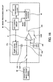
- FIG. 16 shows a part of an imaging circuit using a solid-state image pickup device.
- the imaging circuit includes a solid-state image pickup device 80 and an image processing circuit 90.
- the image processing circuit 90 includes a switch sw91 for connecting or disconnecting the solid-state image pickup device 80, a differential amplifier (comparator) 91, a ramp signal supply source 91a for supplying a ramp signal, a capacitor C91 connected to a non-inverting input terminal of the differential amplifier 91, a capacitor C92 connected to an inverting input terminal, a switch sw92 for connecting or disconnecting the output terminal and the inverting input terminal of the differential amplifier 91, an increment counter 92 for counting up in accordance with the output value of the differential amplifier 91, an AD conversion clock 93 for supplying an operation clock signal to the increment counter 92, and an ADC control circuit 94 for controlling AD conversion by supplying a reset signal to the increment counter 92 or the like.
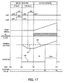
- FIG. 17 is a timing chart illustrating the conventional operation of the imaging circuit.
- n91 a connection node between the non-inverting input terminal of the differential amplifier 91 and the capacitor C91
- n92 a connection node between the inverting input terminal and the capacitor C92
- n93 a connection node between the output terminal of the differential amplifier 91 and the increment counter 92
- noise reading (N Read) is performed first, and the capacitor C92, connected to the inverting input terminal, holds the voltage equivalent to the noise voltage (T90-to-T91 time segment).
- the AD conversion clock 93 is activated (in a shaded portion in the figure), and the potential of the non-inverting input terminal coupled to a capacitor is driven by a ramp signal, thereby ramping up the signal-plus-noise voltage in the direction of the noise voltage.
- the counter counts up until the output of the differential amplifier is inverted and stops when the output is inverted, thereby performing AD conversion (T92-to-T93 time segment).
- an encoded value (digital output value) output from the image processing circuit 90 equals the counter value counted by the increment counter 92.
- the imaging circuit generate an imaging signal with reduced noise.
- One known method to reduce the effect of noise is to use an imaging circuit having a function to cancel out noise generated in a pixel portion of the image pickup device (refer to Japanese Unexamined Patent Application Publication No. 2005-136540 ).
- White noise caused by thermal noise or the like is added to a voltage value encoded in AD conversion. If this white noise is greater than the potential difference per bit (LSB) in AD conversion, the noise component remains in the encoded value. Noise varies with time, causing each pixel having the same brightness, not varying with time, to flicker frame to frame, causing a dark image to become coarse like snow. Recent demands for high resolution and high picture quality create a trend toward a reduced signal per pixel and an increased resolution, worsening the S-N ratio. This problem has become apparent especially in a dark image, having a low S-N ratio.
- an image processing circuit used in an imaging circuit for capturing an image by using a solid-state image pickup device for reading a pixel signal.
- This image processing circuit includes a CDS circuit for taking a potential difference between the pixel signal at a reset of the solid-state image pickup device and the pixel signal after exposure, and an AD conversion circuit including a circuit for performing AD conversion of the potential difference and a processing unit for performing averaging of a plurality of digital code values obtained through the AD conversion repeated a plurality of times.
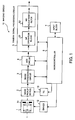
- FIG. 1 is a block diagram showing an essential structure of an imaging circuit according to an embodiment of the present invention.
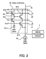
- FIG. 2 is a view showing a part of an image pickup device.
- FIG. 3 is a view showing an image processing circuit.
- FIG. 4 is a timing chart showing signal processing of a first embodiment.
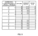
- FIG. 5 is a view (table) showing the relationship between the counter value and the encoded value of the signal processing of the first embodiment.
- FIG. 6 is a timing chart showing signal processing of a second embodiment.
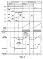
- FIG. 7 is a timing chart showing signal processing of a third embodiment.
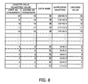
- FIG. 8 is a view (table) showing the relationship between the counter value and the encoded value of the signal processing of the third embodiment.
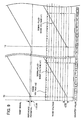
- FIG. 9 is an enlarged view of an essential part of a timing chart showing signal processing of a fourth embodiment.
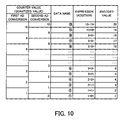
- FIG. 10 is a view (table) showing the relationship between the counter value and the encoded value of the signal processing of the fourth embodiment.
- FIG. 11 is a view showing ramp signals of signal processing of a fifth embodiment.
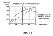
- FIG. 12 is a view showing the relationship between the brightness (luminance) and the encoded value of the signal processing of the fifth embodiment.
- FIG. 13 is a schematic diagram showing a pixel portion of an imaging circuit of a sixth embodiment.
- FIG. 14 is a timing chart showing signal processing in the imaging circuit of the sixth embodiment.
- FIG. 15 is a block diagram showing functions of an electronic device according to an embodiment.
- FIG. 16 is a view showing a part of an imaging circuit using a solid-state image pickup device.
- FIG. 17 is a timing chart showing a conventional operation of the imaging circuit.
- FIG. 1 is a block diagram showing the main components of an imaging circuit according to an embodiment of the present invention.
- the imaging circuit 10 shown in FIG. 1 includes an optical block 1, an image pickup device 2, an image processing circuit 3, an automatic gain control (AGC) circuit 4, a camera signal processing circuit 5, a microcontroller 6, and an input block 7.
- the imaging circuit 10 includes also a driver 12 for driving the mechanism such as a diaphragm 11 in the optical block 1, a timing generator (TG) 13 for driving the image pickup device 2, and the like.
- the optical block 1 includes a lens for collecting light from an object to be imaged onto the image pickup device 2, a drive mechanism for moving the lens for focusing and zooming, a mechanical shutter, and the diaphragm 11, and the like.
- the driver 12 drives the internal mechanism of the optical block 1 in accordance with a control signal from the microcontroller 6.
- the image pickup device 2 is a solid-state image pickup device of a charge-coupled device (CCD) type, a complementary metal oxide semiconductor (CMOS) type, or the like, and is driven to convert incident light from the object to an electric signal in accordance with a timing signal output from the TG 13.
- the TG 13 outputs the timing signal as controlled by the microcontroller 6.
- the image processing circuit 3 includes a correlated double sampling (CDS) circuit for performing sample-hold processing to maintain a good S-N ratio by applying CDS processing to an image signal output from the image pickup device 2 and an AD conversion circuit for performing AD conversion and outputting a digital image signal, the circuits being controlled by the microcontroller 6.
- CDS correlated double sampling
- the AGC circuit 4 performs gain-up processing for the digital image signal output from the image processing circuit 3, under the control of the microcontroller 6.
- the AGC processing may be performed for an analog image signal before AD conversion by the image processing circuit 3.
- the camera signal processing circuit 5 performs auto-focus (AF) processing, auto-exposure (AE) processing, white balance adjustment, and other camera signal processing on an image signal output from the AGC circuit 4 or performs a part of the processing.
- the camera signal processing circuit 5 includes a linear matrix (LM) operation block 51 for performing a matrix operation on each color component of an input image signal and a white balance (WB) adjustment block 52 for adjusting the gain of each color component.
- LM linear matrix
- WB white balance
- the microcontroller 6 includes, for instance, a central processing unit (CPU), a read-only memory (ROM), a random access memory (RAM), and the like, and executes a program stored in the ROM or the like to comprehensively control the different blocks of the imaging circuit 10 and to execute operations needed to control them.
- the input block 7 includes operation keys, a dial, a lever, and the like for accepting the operation input of the user, and outputs a control signal depending on the operation input to the microcontroller 6.
- signals photoelectric-converted by the image pickup device 2 from received light are successively supplied to the image processing circuit 3, where they are converted to digital signals and supplied to the AGC circuit 4 for gain adjustment.
- the camera signal processing circuit 5 performs picture quality correction processing on each digital image signal supplied by the AGC circuit 4, converts the signal to a luminance signal and a color-difference signal, and outputs them.
- the image data output from the camera signal processing circuit 5 is supplied to a graphic interface circuit, which is not shown, and converted to a display image signal, by which a through-the-lens image is displayed on a monitor, which is not shown.
- the input block 7 gives the microcontroller 6 an instruction to record the image in accordance with an operation input by the user
- the image data is supplied from the camera signal processing circuit 5 to an encoder-decoder (CODEC), which is not shown, predetermined compression encoding is performed, and the encoded data is recorded on a recording medium, which is not shown.
- CODEC encoder-decoder
- the camera signal processing circuit 5 supplies the image data of one frame to the CODEC.
- the encoded image data is successively supplied to the CODEC.
- FIG. 2 is a view showing a part of the image pickup device 2.
- a pixel portion 20, i.e. one pixel of the image pickup device 2 includes a photodiode (photoelectric transducer) PD11, a transfer transistor M11, an amplifying transistor M12, a selection transistor M13, and a reset transistor M14. These transistors are n-channel MOSFETs.
- the gates of the selection transistor M13, the transfer transistor M11, and the reset transistor M14 are connected to a row selection signal line (SLCT) 21, a transfer signal line (TG signal supply line) 22, and a reset signal line (RST) 23, respectively. These signal lines are laid horizontally and drive the pixels in the same row simultaneously. This enables a rolling shutter of line progressive operation type and a global shutter, which works on all pixels simultaneously, to be provided.
- the source of the selection transistor M13 is connected to a vertical signal line 24, and the other end of the vertical signal line 24 is grounded through a constant-current power supply 25.
- the vertical signal line 24 is also connected to the image processing circuit 3.
- the photodiode PD11 accumulates an electric charge generated by photoelectric conversion, having a positive terminal grounded and a negative terminal connected to the source of the transfer transistor M11.
- the transfer transistor M11 When the transfer transistor M11 is turned on, the electric charge of the photodiode PD11 is transferred to FD26, where the electric charge is accumulated.
- the amplifying transistor M12 has a drain connected to a source voltage line (VR) 27 and a gate connected to the FD26.
- the amplifying transistor M12 converts a varying potential at the FD26 into an electric signal.
- the selection transistor M13 is provided to select a row of pixels to be read, having a drain connected to the source of the amplifying transistor M12 and the source, connected to the vertical signal line 24. When the selection transistor M13 is turned on, the amplifying transistor M12 and the constant-current power supply 25 form a source follower and outputs a voltage determined by the voltage at the FD26 to the vertical signal line 24.
- the reset transistor M14 has a drain connected to the source voltage line 27 and a source connected to the FD26. The reset transistor M14 resets the potential at the FD26 to the supply voltage.
- This circuit can perform two types of electronic shutter operations: rolling shutter and global shutter.
- pulse signals are sent to the reset signal line 23 and the transfer signal line 22 to turn on the reset transistor M14 and the transfer transistor M11 to reset the FD26 and the photodiode PD11.
- the exposure period of the photodiode PD11 starts.
- the reset signal line 23 of the row is brought high to turn on the reset transistor M14, setting the FD26 to the supply voltage VR.
- the row selection signal line 21 of the row is brought high to turn on the selection transistor M13 to output a voltage corresponding to the reset voltage of the FD26 to the vertical signal line 24.
- the reset signal line 23 is brought low to turn off the reset transistor M14, and then the transfer signal line 22 is brought high to turn on the transfer transistor M11. This ends the exposure period.
- the voltage proportional to the charge accumulated in the photodiode PD11 is transferred to the FD26, and a voltage corresponding to the voltage at the FD26 is output to the vertical signal line 24.
- the difference between the voltage corresponding to the reset voltage and that of the voltage proportional to the accumulated charge becomes a signal voltage, and the signal voltage is extracted by the CDS processing of the CDS circuit.
- the reset transistor M14 and the transfer transistor M11 are turned on and off. Then, the next exposure period starts.
- the above-described operations are performed one row after another with a delay in synchronization with a horizontal synchronizing signal, starting from the first row, and the pixel signals of the rows are output successively.
- the exposure period of each row is delayed from that of the previous row.
- the reset transistor M14 and the transfer transistor M11 are turned on to reset the FD26 and the photodiode PD11 for all rows at the same time. Accordingly, the exposure periods of all rows start simultaneously.
- FIG. 3 is a view showing the image processing circuit 3.
- the image processing circuit 3 includes a CDS circuit 3a and an AD conversion circuit 3b, as described earlier.
- FIG. 3 shows the configuration of a CDS circuit for one column of the pixel portions 20.
- the CDS circuit 3a includes a sample-hold switch sw1 for controlling the input of an image signal output from the pixel portion 20.
- the output of the sample-hold switch sw1 is connected to a capacitor (sample-hold capacitor) C31 for holding the image signal.
- the other side of the capacitor C31 is connected to a ramp signal supply source 31a for supplying a ramp signal for changing the potential of the image signal held in the capacitor C31.
- a node n1 between the sample-hold switch sw1 and the capacitor C31 is connected to a non-inverting input terminal of a differential amplifier 33a.
- a capacitor C32 is provided between an inverting input terminal of the differential amplifier 33a and the ground.
- a clamp switch sw2 is disposed between the output terminal of the differential amplifier 33a and a node n2, which is disposed between the inverting input terminal and the capacitor C32.
- the output terminal of the differential amplifier 33a is connected to the AD conversion circuit 3b.
- the AD conversion circuit 3b includes an increment counter 31b, an AD conversion clock 32b for supplying a clock signal to the increment counter 31b, and an averaging ADC control circuit 33b for controlling the whole of the AD conversion circuit 3b.
- the increment counter 31b counts up when the clock signal is supplied from the AD conversion clock 32b and when a positive signal is output from the output terminal of the differential amplifier 33a.
- the averaging ADC control circuit 33b performs averaging, which will be described later, in AD conversion and calculates an encoded value.
- the averaging ADC control circuit 33b also sends the ramp signal supply source 31a timings to start, stop, and reset the ramp signal, sends a counter reset signal to the increment counter 31b, and sends the AD conversion clock 32b timings to start, stop, and reset the clock.
- FIG. 4 is a timing chart showing the signal processing of the first embodiment.
- Noise reading is first performed in the initial reading (T0-to-T1 time segment).
- a pixel is selected by bringing the row selection signal line (SLCT) 21 high, and the reset signal line 23 is brought low.
- the sample-hold switch sw1 is turned on, and the clamp switch sw2 is turned on.
- the sample-hold switch sw1 causes the noise voltage of the pixel to be input to the non-inverting input terminal of the differential amplifier 33a.
- Turning on the clamp switch sw2 causes a voltage corresponding to the noise voltage to be held (stored) in the capacitor C32, connected to the inverting input terminal.
- the offset potential between the non-inverting input terminal and the inverting input terminal of the differential amplifier 33a is included in the voltages at the input terminals and held in the capacitor C32, connected to the inverting input terminal, and the offset potential is cancelled in subsequent operations.
- Signal-plus-noise reading (S+N Read) is performed next (T1-to-T2 time segment).
- the clamp switch sw2 is turned off to release Auto-Zero, and the noise voltage at the inverting input terminal is held.
- the sample-hold switch sw1 is turned off to produce no effect on the pixel transfer operation from the AD conversion circuit 3b.
- the transfer signal line 22 of the pixel is brought high to transfer the read potential, then the sample-hold switch sw1 is turned on to input the signal-plus-noise voltage to the non-inverting input terminal.
- AD conversion is performed (T2-to-T5 time segment).
- the sample-hold switch sw1 is turned off to hold the signal-plus-noise voltage at the non-inverting input terminal.
- the AD conversion clock is activated (in shaded portions in FIG. 4) to drive the potential at the non-inverting input terminal connected to a capacitor by a ramp signal and to ramp up the signal-plus-noise voltage in the direction of noise voltage.
- the counter counts up until the output of the differential amplifier is inverted and stops when the inversion occurs, thereby AD conversion is performed.
- the resolution of a single AD conversion is halved in the T2-to-T5 time segment (unit time), and the AD conversion is carried out twice (a plurality of times). Accordingly, noise is read in the initial reading, and the result is held in the capacitor C32.
- a first AD conversion is performed as described earlier (T2-to-T3 time segment). Then, the sample-hold switch sw1 is turned on again to perform signal-plus-noise reading again (T3-to-T4 time segment). A second AD conversion is performed next (T4-to-T5 time segment). After the second signal-plus-noise reading is performed, the row selection signal line 21 is brought low.
- FIG. 5 is a view (table) showing the relationship between the counter value and the encoded value of the signal processing of the first embodiment.
- FIG. 5 has columns of counter value, data name, expression (addition), and encoded value.
- the items in a horizontal row are related to one another.
- the counter value column is divided into two columns of first AD conversion and second AD conversion.
- Count values (quantized values) obtained in the first AD conversion and the second AD conversion are recorded in the corresponding columns.
- the LSB is doubled because the resolution of AD conversion is half of that when a single AD conversion is performed in the unit time. As a result, the encoded value changes every two conversions.
- AD conversion is carried out a plurality of times during a unit of time in which the pixel signal of one row is read once.
- the capacitor C32 is not discharged nor re-charged, and the sum of the obtained count values is taken.
- the count value per bit obtained in the first AD conversion and the count value per bit obtained in the second AD conversion are added (and averaged) to obtain each encoded value.
- noise component is reduced by averaging data that includes different noise.
- noise is reduced by averaging the counter values of different time series, without increasing the processing time greatly (just increasing the time for performing signal-plus-noise reading again), so that a change in noise component over time can be reduced. Because white noise of a dark image is reduced especially, the image is prevented from becoming coarse, or the coarse level of the image is suppressed. The quality of the image can be improved.
- Signal-plus-noise reading is performed again after the first AD conversion ends, so that the signal-plus-noise read value does not deteriorate. Accordingly, a correct encoded value can be obtained.
- FIG. 6 is a timing chart showing the signal processing of the second embodiment.
- the signal processing of the second embodiment differs from the signal processing of the first embodiment in that the sample-hold switch sw1 is not turned on or off before the second AD conversion (T3-to-T4 time segment), that is, signal-plus-noise reading is not performed again.
- the voltage held in the capacitor C31 in the first processing is used as the signal-plus-noise voltage of the second AD conversion.
- the value held in the capacitor C32 and used in the first processing is used as the noise voltage.
- Noise is reduced in the signal processing of the second embodiment, and the image is prevented from becoming coarse, or the coarse level of the image is suppressed in comparison with the conventional processing.
- the image quality can be improved.
- FIG. 7 is a timing chart showing the signal processing of the third embodiment.
- the time period per AD conversion is twice that in the first embodiment or the second embodiment, and two AD conversions are carried out.
- the time period required to carry out one AD conversion in the third embodiment corresponds to the T2-to-T4a time segment of the second embodiment.
- FIG. 8 is a view (table) showing the relationship between the counter value and the encoded value of the signal processing of the third embodiment.
- the signal processing of the third embodiment has double the resolution per AD conversion (the same resolution as the conventional signal processing), so that an encoded value can be obtained by averaging the resultant counter values.
- the signal processing of the third embodiment produces the same advantages as the signal processing of the first embodiment and the second embodiment.
- the signal processing of the third embodiment has substantially the same resolution of AD conversion as the conventional processing, so that a change in noise component over time can be reduced, and high-precision conversion can be carried out, producing a high-precision image.
- One characteristic of the signal processing of the fourth embodiment is that the second AD conversion is carried out with the initial potential (offset potential) of the ramp signal shifted by an amount corresponding to LSB/2.
- FIG. 9 is an enlarged view of an essential part of a timing chart showing the signal processing of the fourth embodiment.
- the second AD conversion starts with the initial potential of the ramp signal being shifted by an amount corresponding to LSB/2 of the AD conversion circuit 3b.
- the information of the initial potential of the second AD conversion is stored in the microcontroller 6 beforehand.
- FIG. 10 is a view showing the relationship between the counter value and the encoded value of the signal processing of the fourth embodiment.
- the second AD conversion since the second AD conversion starts with the initial potential being shifted by the amount corresponding to LSB/2, the second counter value of each bit is shifted from the first counter value by LSB/2.
- the counter values of the first AD conversion and the corresponding counter values of the second AD conversion are added to obtain the encoded values of the fourth embodiment.
- the signal processing of the fourth embodiment produces the same advantages as the signal processing of the first embodiment.
- the AD conversion has the same resolution as the conventional AD conversion, as clearly indicated in FIG. 10. Accordingly, a change in noise component over time can be reduced without lowering the resolution. If three (n) AD conversions are performed in the unit time, the second (n-1-th) AD conversion is performed with the initial potential being shifted by an amount corresponding to 1/3 (1/n) LSB from the first (n-2-th) AD conversion, and the third (n-th) AD conversion is performed with the initial potential shifted by an amount corresponding to 1/3 (1/n) LSB from the second (n-1-th) AD conversion.
- FIG. 11 is a view showing ramp signals used in the signal processing of the fifth embodiment.
- brightness levels 0 to 288 are counted fourth (four times) (0 to 144, 144 to 288, 288 to 432, 576 to 720) at a resolution of 144 and are added, so that an encoded value of 0 to 576 (144 4) is assigned.
- Brightness levels 288 to 576 are counted twice (288 to 576, 576 to 864) at a resolution of 144 and are added, so that an encoded value of 576 to 864 (576 + 144 ' 2) is assigned.
- Brightness levels 576 to 1152 are counted once (576 to 1152) at a resolution of 144, so that an encoded value of 864 to 1152 (864 + 288 ' 1) is assigned.
- FIG. 12 is a view (table) showing the relationship between the brightness (luminance) and the encoded value of the signal processing of the fifth embodiment.
- a dashed line in FIG. 12 represents the encoded value (output value) of the AD conversion circuit 3b of the first to third embodiments.
- a solid line represents the encoded value of the AD conversion circuit 3b of the fifth embodiment.
- the number of times of AD conversion increases as the brightness value decreases, that is, as the S-N ratio decreases, so that noise can be suppressed in a dark area, where human visual perception is generally high.
- the imaging circuit of the sixth embodiment will be described next, with differences from the imaging circuit 10 of the first embodiment being stressed, and a description of common items omitted.
- the imaging circuit of the sixth embodiment differs from the imaging circuit 10 of the first embodiment in the structure of each pixel, in other words of the pixel portion.
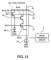
- FIG. 13 is a schematic diagram showing the pixel portion of the imaging circuit of the sixth embodiment.
- the imaging circuit of the sixth embodiment includes a so-called tri-transistor pixel portion 20a.
- the pixel portion 20a includes a photodiode PD11, a reset transistor M11a for resetting the cathode of the photodiode PD11 to an initial voltage, an amplifying transistor M12a for converting a charge accumulated in the photodiode PD11 to a voltage, and a selection transistor M13a for outputting the output voltage of the amplifying transistor M12a as the image signal of a single pixel in accordance with a row selection signal for selecting the signal outputs from pixel portions arranged in rows.
- CMOS image sensor when the reset transistor M11a is turned on, the potential of the cathode of the photodiode PD11a is specified as the initial voltage, and the charge accumulated in the photodiode PD11a is reset.
- FIG. 14 is a timing chart showing signal processing in the imaging circuit of the sixth embodiment.
- AD conversion is performed with the signal-plus-noise voltage held in the capacitor C32 and the noise voltage held in the capacitor C31.
- the imaging circuit of the sixth embodiment produces the same advantages as the imaging circuit of the first embodiment. Since the imaging circuit of the sixth embodiment includes the tri-transistor pixel portion 20a, a reduced circuit footprint can be used. Because a large sub-pixel portion can be taken, the aperture ratio and transmittance can be improved.
- FIG. 15 is a block diagram showing the functions of the electronic device of the present embodiment.
- FIG. 15 shows a portable terminal 100, as an example of the electronic device.
- the portable terminal 100 includes a CPU 40, an input block 50, a display block 60, an imaging circuit 10, and a communication block 70.
- the imaging circuit 10 and the communication block 70 are connected through a bus.
- the CPU 40 controls the operations of the imaging circuit 10 and the communication block 70.
- the input block 50 includes keys such as numeric keys and function keys and accepts the input of a telephone number, a command, and the like.
- the display block 60 displays various pieces of information output by the CPU 40.
- the communication block 70 includes a transfer memory 71, a transmission-destination registration memory 72, a PCMCODEC and tone-ringer section 73, a microphone 73a, a speaker 73b, an ADPCM conversion section 74, a time division multiple access control section 75, a modem 76, a radio section 77, and an antenna 78.
- the transfer memory 71 forms a temporary storage unit for holding image information transmitted from the imaging circuit 10 temporarily.
- the transmission-destination registration memory 72 forms a storage unit for storing information of a transmission destination.
- the PCMCODEC and tone-ringer section 73 outputs a tone ringer signal and a PCMCODEC signal for performing mutual conversion between an analog signal and a digital signal.
- the microphone 73a and the speaker 73b are connected to the PCMCODEC and tone-ringer section 73.
- the ADPCM conversion section 74 compresses and decompresses sound.
- the ADPCM conversion section 74 compresses a sound signal to be transmitted and decompresses a received sound signal.
- the time division multiple access control section 75 assembles a time division multiple frame from audio data, control data, image data, and the like, or disassembles the frame.
- the time division multiple access control section 75 exchanges an identification (ID) number with a radio base station continuously or intermittently.
- the time division multiple access control section 75 also detects the current position from communication information of the communication block 70.
- the modem 76 modulates and demodulates a transfer signal.
- the radio section 77 is connected to the modem 76 and performs radio communication of information.
- the antenna 78 is an antenna for radio transmission.
- the CPU 40 selects a transmission destination from a transmission-destination list stored in the transmission-destination registration memory 72 in accordance with information from the time division multiple access control section 75.
- the modem 76 and the radio section 77 send image information from the transfer memory 71 in accordance with information sent from the CPU 40.
- two or more embodiments (features) of the present invention may be combined.
- the signal processing of the fourth embodiment may be applied to the signal processing of the second and third embodiments.
- the imaging circuit according to the present invention can be applied to various types of electronic devices, in addition to the portable terminal shown in FIG. 15.
- a plurality of digital code values obtained through several repeated AD conversions is averaged, so that noise of the pixel signal can be reduced.
Landscapes
- Engineering & Computer Science (AREA)
- Multimedia (AREA)
- Signal Processing (AREA)
- Transforming Light Signals Into Electric Signals (AREA)
- Facsimile Image Signal Circuits (AREA)
Abstract
Description
- The present invention relates to image processing circuits, imaging circuits, and electronic devices, and particularly to an image processing circuit, an imaging circuit, and an electronic device for use in processing a captured image.
- In recent years, digital still cameras and digital video cameras have become widespread, and mobile phones have incorporated camera functions, so that imaging circuits equipped with a solid-state image pickup device have grown in demand.
- FIG. 16 shows a part of an imaging circuit using a solid-state image pickup device.
- The imaging circuit includes a solid-state
image pickup device 80 and animage processing circuit 90. - The
image processing circuit 90 includes a switch sw91 for connecting or disconnecting the solid-stateimage pickup device 80, a differential amplifier (comparator) 91, a rampsignal supply source 91a for supplying a ramp signal, a capacitor C91 connected to a non-inverting input terminal of thedifferential amplifier 91, a capacitor C92 connected to an inverting input terminal, a switch sw92 for connecting or disconnecting the output terminal and the inverting input terminal of thedifferential amplifier 91, anincrement counter 92 for counting up in accordance with the output value of thedifferential amplifier 91, anAD conversion clock 93 for supplying an operation clock signal to theincrement counter 92, and anADC control circuit 94 for controlling AD conversion by supplying a reset signal to theincrement counter 92 or the like. - The conventional operation of the imaging circuit will be described next.
- FIG. 17 is a timing chart illustrating the conventional operation of the imaging circuit.
- In FIG. 17, a connection node between the non-inverting input terminal of the
differential amplifier 91 and the capacitor C91 is denoted as n91; a connection node between the inverting input terminal and the capacitor C92 is denoted as n92; and a connection node between the output terminal of thedifferential amplifier 91 and theincrement counter 92 is denoted as n93. - First, initial reading is carried out. To be more specific, noise reading (N Read) is performed first, and the capacitor C92, connected to the inverting input terminal, holds the voltage equivalent to the noise voltage (T90-to-T91 time segment).
- Then, signal-plus-noise reading (S+N Read) is performed, and the signal-plus-noise voltage is input to the non-inverting input terminal of the differential amplifier 91 (T91-to-T92 time segment). These operations give the noise voltage to the inverting input terminal and the signal-plus-noise voltage to the non-inverting input terminal, bringing the potential difference between the two input terminals to the signal voltage.
- Next, the switch sw91 is turned off, and the signal-plus-noise voltage is held at the non-inverting input terminal. This operation ends the initial reading.
- The
AD conversion clock 93 is activated (in a shaded portion in the figure), and the potential of the non-inverting input terminal coupled to a capacitor is driven by a ramp signal, thereby ramping up the signal-plus-noise voltage in the direction of the noise voltage. The counter counts up until the output of the differential amplifier is inverted and stops when the output is inverted, thereby performing AD conversion (T92-to-T93 time segment). - In the conventional operation, an encoded value (digital output value) output from the
image processing circuit 90 equals the counter value counted by theincrement counter 92. - It is increasingly required that the imaging circuit generate an imaging signal with reduced noise. One known method to reduce the effect of noise is to use an imaging circuit having a function to cancel out noise generated in a pixel portion of the image pickup device (refer to
Japanese Unexamined Patent Application Publication No. 2005-136540 - In the conventional operation, however, white noise caused by thermal noise or the like causes images with a low signal-to-noise ratio, such as a dark image, to become coarse, like snow.
- White noise caused by thermal noise or the like is added to a voltage value encoded in AD conversion. If this white noise is greater than the potential difference per bit (LSB) in AD conversion, the noise component remains in the encoded value. Noise varies with time, causing each pixel having the same brightness, not varying with time, to flicker frame to frame, causing a dark image to become coarse like snow. Recent demands for high resolution and high picture quality create a trend toward a reduced signal per pixel and an increased resolution, worsening the S-N ratio. This problem has become apparent especially in a dark image, having a low S-N ratio.
- In view of the foregoing, it is desirable to provide an image processing circuit, an imaging circuit, and an electronic device that can reduce noise.
- According to one aspect of the present invention, there is provided an image processing circuit used in an imaging circuit for capturing an image by using a solid-state image pickup device for reading a pixel signal. This image processing circuit includes a CDS circuit for taking a potential difference between the pixel signal at a reset of the solid-state image pickup device and the pixel signal after exposure, and an AD conversion circuit including a circuit for performing AD conversion of the potential difference and a processing unit for performing averaging of a plurality of digital code values obtained through the AD conversion repeated a plurality of times.
- The above and other features and advantages of the present invention will become apparent from the following description when taken in conjunction with the accompanying drawings which illustrate preferred embodiments of the present invention by way of example, and in which:
- FIG. 1 is a block diagram showing an essential structure of an imaging circuit according to an embodiment of the present invention.
- FIG. 2 is a view showing a part of an image pickup device.
- FIG. 3 is a view showing an image processing circuit.
- FIG. 4 is a timing chart showing signal processing of a first embodiment.
- FIG. 5 is a view (table) showing the relationship between the counter value and the encoded value of the signal processing of the first embodiment.
- FIG. 6 is a timing chart showing signal processing of a second embodiment.
- FIG. 7 is a timing chart showing signal processing of a third embodiment.
- FIG. 8 is a view (table) showing the relationship between the counter value and the encoded value of the signal processing of the third embodiment.
- FIG. 9 is an enlarged view of an essential part of a timing chart showing signal processing of a fourth embodiment.
- FIG. 10 is a view (table) showing the relationship between the counter value and the encoded value of the signal processing of the fourth embodiment.
- FIG. 11 is a view showing ramp signals of signal processing of a fifth embodiment.
- FIG. 12 is a view showing the relationship between the brightness (luminance) and the encoded value of the signal processing of the fifth embodiment.
- FIG. 13 is a schematic diagram showing a pixel portion of an imaging circuit of a sixth embodiment.
- FIG. 14 is a timing chart showing signal processing in the imaging circuit of the sixth embodiment.
- FIG. 15 is a block diagram showing functions of an electronic device according to an embodiment.
- FIG. 16 is a view showing a part of an imaging circuit using a solid-state image pickup device.
- FIG. 17 is a timing chart showing a conventional operation of the imaging circuit.
- Embodiments of the present invention will be described below in detail with reference to the drawings.
- FIG. 1 is a block diagram showing the main components of an imaging circuit according to an embodiment of the present invention.
- The
imaging circuit 10 shown in FIG. 1 includes anoptical block 1, animage pickup device 2, animage processing circuit 3, an automatic gain control (AGC)circuit 4, a camerasignal processing circuit 5, amicrocontroller 6, and aninput block 7. Theimaging circuit 10 includes also adriver 12 for driving the mechanism such as adiaphragm 11 in theoptical block 1, a timing generator (TG) 13 for driving theimage pickup device 2, and the like. - The
optical block 1 includes a lens for collecting light from an object to be imaged onto theimage pickup device 2, a drive mechanism for moving the lens for focusing and zooming, a mechanical shutter, and thediaphragm 11, and the like. Thedriver 12 drives the internal mechanism of theoptical block 1 in accordance with a control signal from themicrocontroller 6. - The
image pickup device 2 is a solid-state image pickup device of a charge-coupled device (CCD) type, a complementary metal oxide semiconductor (CMOS) type, or the like, and is driven to convert incident light from the object to an electric signal in accordance with a timing signal output from theTG 13. TheTG 13 outputs the timing signal as controlled by themicrocontroller 6. - The
image processing circuit 3 includes a correlated double sampling (CDS) circuit for performing sample-hold processing to maintain a good S-N ratio by applying CDS processing to an image signal output from theimage pickup device 2 and an AD conversion circuit for performing AD conversion and outputting a digital image signal, the circuits being controlled by themicrocontroller 6. - The
AGC circuit 4 performs gain-up processing for the digital image signal output from theimage processing circuit 3, under the control of themicrocontroller 6. The AGC processing may be performed for an analog image signal before AD conversion by theimage processing circuit 3. - The camera
signal processing circuit 5 performs auto-focus (AF) processing, auto-exposure (AE) processing, white balance adjustment, and other camera signal processing on an image signal output from theAGC circuit 4 or performs a part of the processing. In the present embodiment, the camerasignal processing circuit 5 includes a linear matrix (LM)operation block 51 for performing a matrix operation on each color component of an input image signal and a white balance (WB)adjustment block 52 for adjusting the gain of each color component. - The
microcontroller 6 includes, for instance, a central processing unit (CPU), a read-only memory (ROM), a random access memory (RAM), and the like, and executes a program stored in the ROM or the like to comprehensively control the different blocks of theimaging circuit 10 and to execute operations needed to control them. Theinput block 7 includes operation keys, a dial, a lever, and the like for accepting the operation input of the user, and outputs a control signal depending on the operation input to themicrocontroller 6. - In the
imaging circuit 10, signals photoelectric-converted by theimage pickup device 2 from received light are successively supplied to theimage processing circuit 3, where they are converted to digital signals and supplied to theAGC circuit 4 for gain adjustment. The camerasignal processing circuit 5 performs picture quality correction processing on each digital image signal supplied by theAGC circuit 4, converts the signal to a luminance signal and a color-difference signal, and outputs them. - The image data output from the camera
signal processing circuit 5 is supplied to a graphic interface circuit, which is not shown, and converted to a display image signal, by which a through-the-lens image is displayed on a monitor, which is not shown. If theinput block 7 gives themicrocontroller 6 an instruction to record the image in accordance with an operation input by the user, the image data is supplied from the camerasignal processing circuit 5 to an encoder-decoder (CODEC), which is not shown, predetermined compression encoding is performed, and the encoded data is recorded on a recording medium, which is not shown. When a still image is recorded, the camerasignal processing circuit 5 supplies the image data of one frame to the CODEC. When moving images are recorded, the encoded image data is successively supplied to the CODEC. - FIG. 2 is a view showing a part of the
image pickup device 2. - As shown in FIG. 2, a
pixel portion 20, i.e. one pixel of theimage pickup device 2, includes a photodiode (photoelectric transducer) PD11, a transfer transistor M11, an amplifying transistor M12, a selection transistor M13, and a reset transistor M14. These transistors are n-channel MOSFETs. - The gates of the selection transistor M13, the transfer transistor M11, and the reset transistor M14 are connected to a row selection signal line (SLCT) 21, a transfer signal line (TG signal supply line) 22, and a reset signal line (RST) 23, respectively. These signal lines are laid horizontally and drive the pixels in the same row simultaneously. This enables a rolling shutter of line progressive operation type and a global shutter, which works on all pixels simultaneously, to be provided. The source of the selection transistor M13 is connected to a
vertical signal line 24, and the other end of thevertical signal line 24 is grounded through a constant-current power supply 25. Thevertical signal line 24 is also connected to theimage processing circuit 3. - The photodiode PD11 accumulates an electric charge generated by photoelectric conversion, having a positive terminal grounded and a negative terminal connected to the source of the transfer transistor M11. When the transfer transistor M11 is turned on, the electric charge of the photodiode PD11 is transferred to FD26, where the electric charge is accumulated.
- The amplifying transistor M12 has a drain connected to a source voltage line (VR) 27 and a gate connected to the FD26. The amplifying transistor M12 converts a varying potential at the FD26 into an electric signal. The selection transistor M13 is provided to select a row of pixels to be read, having a drain connected to the source of the amplifying transistor M12 and the source, connected to the
vertical signal line 24. When the selection transistor M13 is turned on, the amplifying transistor M12 and the constant-current power supply 25 form a source follower and outputs a voltage determined by the voltage at the FD26 to thevertical signal line 24. - The reset transistor M14 has a drain connected to the
source voltage line 27 and a source connected to the FD26. The reset transistor M14 resets the potential at the FD26 to the supply voltage. - The operation of the
pixel portion 20 of the present embodiment will be described next. - This circuit can perform two types of electronic shutter operations: rolling shutter and global shutter.
- In the rolling shutter operation, at each
pixel portion 20 in a row, pulse signals are sent to thereset signal line 23 and thetransfer signal line 22 to turn on the reset transistor M14 and the transfer transistor M11 to reset the FD26 and the photodiode PD11. When these transistors are turned off, the exposure period of the photodiode PD11 starts. - Immediately before the exposure period ends, the
reset signal line 23 of the row is brought high to turn on the reset transistor M14, setting the FD26 to the supply voltage VR. In this state, the rowselection signal line 21 of the row is brought high to turn on the selection transistor M13 to output a voltage corresponding to the reset voltage of the FD26 to thevertical signal line 24. Next, thereset signal line 23 is brought low to turn off the reset transistor M14, and then thetransfer signal line 22 is brought high to turn on the transfer transistor M11. This ends the exposure period. The voltage proportional to the charge accumulated in the photodiode PD11 is transferred to the FD26, and a voltage corresponding to the voltage at the FD26 is output to thevertical signal line 24. - The difference between the voltage corresponding to the reset voltage and that of the voltage proportional to the accumulated charge becomes a signal voltage, and the signal voltage is extracted by the CDS processing of the CDS circuit.
- After the selection transistor M13 and the transfer transistor M11 are turned off, the reset transistor M14 and the transfer transistor M11 are turned on and off. Then, the next exposure period starts. The above-described operations are performed one row after another with a delay in synchronization with a horizontal synchronizing signal, starting from the first row, and the pixel signals of the rows are output successively. The exposure period of each row is delayed from that of the previous row.
- In the global shutter operation, the reset transistor M14 and the transfer transistor M11 are turned on to reset the FD26 and the photodiode PD11 for all rows at the same time. Accordingly, the exposure periods of all rows start simultaneously.
- If a mechanical shutter is used, when the exposure period ends, charges accumulated in the photodiodes PD11 of each row are successively transferred to the FD26, and the signal voltages of each row are output to the
vertical signal lines 24, as in the rolling shutter operation. - FIG. 3 is a view showing the
image processing circuit 3. - The
image processing circuit 3 includes aCDS circuit 3a and anAD conversion circuit 3b, as described earlier. - FIG. 3 shows the configuration of a CDS circuit for one column of the
pixel portions 20. - The
CDS circuit 3a includes a sample-hold switch sw1 for controlling the input of an image signal output from thepixel portion 20. The output of the sample-hold switch sw1 is connected to a capacitor (sample-hold capacitor) C31 for holding the image signal. The other side of the capacitor C31 is connected to a rampsignal supply source 31a for supplying a ramp signal for changing the potential of the image signal held in the capacitor C31. - A node n1 between the sample-hold switch sw1 and the capacitor C31 is connected to a non-inverting input terminal of a
differential amplifier 33a. - A capacitor C32 is provided between an inverting input terminal of the
differential amplifier 33a and the ground. A clamp switch sw2 is disposed between the output terminal of thedifferential amplifier 33a and a node n2, which is disposed between the inverting input terminal and the capacitor C32. The output terminal of thedifferential amplifier 33a is connected to theAD conversion circuit 3b. - The
AD conversion circuit 3b includes anincrement counter 31b, anAD conversion clock 32b for supplying a clock signal to theincrement counter 31b, and an averagingADC control circuit 33b for controlling the whole of theAD conversion circuit 3b. - The
increment counter 31b counts up when the clock signal is supplied from theAD conversion clock 32b and when a positive signal is output from the output terminal of thedifferential amplifier 33a. - The averaging
ADC control circuit 33b performs averaging, which will be described later, in AD conversion and calculates an encoded value. - The averaging
ADC control circuit 33b also sends the rampsignal supply source 31a timings to start, stop, and reset the ramp signal, sends a counter reset signal to theincrement counter 31b, and sends theAD conversion clock 32b timings to start, stop, and reset the clock. - Signal processing according to a first embodiment will be described next.
- FIG. 4 is a timing chart showing the signal processing of the first embodiment.
- First, initial reading is performed. Noise reading (N Read) is first performed in the initial reading (T0-to-T1 time segment). To be more specific, a pixel is selected by bringing the row selection signal line (SLCT) 21 high, and the
reset signal line 23 is brought low. At the same time, the sample-hold switch sw1 is turned on, and the clamp switch sw2 is turned on. Turning on the sample-hold switch sw1 causes the noise voltage of the pixel to be input to the non-inverting input terminal of thedifferential amplifier 33a. Turning on the clamp switch sw2 causes a voltage corresponding to the noise voltage to be held (stored) in the capacitor C32, connected to the inverting input terminal. The offset potential between the non-inverting input terminal and the inverting input terminal of thedifferential amplifier 33a is included in the voltages at the input terminals and held in the capacitor C32, connected to the inverting input terminal, and the offset potential is cancelled in subsequent operations. - Signal-plus-noise reading (S+N Read) is performed next (T1-to-T2 time segment). The clamp switch sw2 is turned off to release Auto-Zero, and the noise voltage at the inverting input terminal is held. At the same time, the sample-hold switch sw1 is turned off to produce no effect on the pixel transfer operation from the
AD conversion circuit 3b. Thetransfer signal line 22 of the pixel is brought high to transfer the read potential, then the sample-hold switch sw1 is turned on to input the signal-plus-noise voltage to the non-inverting input terminal. These operations give the noise voltage to the inverting input terminal and the signal-plus-noise voltage to the non-inverting input terminal, the potential difference between the two inputs being the signal voltage. The operation up to this point is performed in the same way as the initial reading. - Next, AD conversion is performed (T2-to-T5 time segment). The sample-hold switch sw1 is turned off to hold the signal-plus-noise voltage at the non-inverting input terminal. The AD conversion clock is activated (in shaded portions in FIG. 4) to drive the potential at the non-inverting input terminal connected to a capacitor by a ramp signal and to ramp up the signal-plus-noise voltage in the direction of noise voltage. The counter counts up until the output of the differential amplifier is inverted and stops when the inversion occurs, thereby AD conversion is performed.
- In the present embodiment, the resolution of a single AD conversion is halved in the T2-to-T5 time segment (unit time), and the AD conversion is carried out twice (a plurality of times). Accordingly, noise is read in the initial reading, and the result is held in the capacitor C32. Next, a first AD conversion is performed as described earlier (T2-to-T3 time segment). Then, the sample-hold switch sw1 is turned on again to perform signal-plus-noise reading again (T3-to-T4 time segment). A second AD conversion is performed next (T4-to-T5 time segment). After the second signal-plus-noise reading is performed, the row
selection signal line 21 is brought low. - FIG. 5 is a view (table) showing the relationship between the counter value and the encoded value of the signal processing of the first embodiment.
- FIG. 5 has columns of counter value, data name, expression (addition), and encoded value. The items in a horizontal row are related to one another.
- The counter value column is divided into two columns of first AD conversion and second AD conversion.
- Count values (quantized values) obtained in the first AD conversion and the second AD conversion are recorded in the corresponding columns.
- In the data name column, a name identifying the encoded value is entered.
- In the expression column, a formula for obtaining the encoded value from the count values is specified.
- In the encoded value column, an obtained encoded value is recorded.
- If two AD conversions are carried out in the unit time, the LSB is doubled because the resolution of AD conversion is half of that when a single AD conversion is performed in the unit time. As a result, the encoded value changes every two conversions.
- As described above, in the present embodiment, AD conversion is carried out a plurality of times during a unit of time in which the pixel signal of one row is read once. Between the first and second AD conversions, the capacitor C32 is not discharged nor re-charged, and the sum of the obtained count values is taken. The count value per bit obtained in the first AD conversion and the count value per bit obtained in the second AD conversion are added (and averaged) to obtain each encoded value.
- It is generally known that a noise component is reduced by averaging data that includes different noise. In this embodiment, noise is reduced by averaging the counter values of different time series, without increasing the processing time greatly (just increasing the time for performing signal-plus-noise reading again), so that a change in noise component over time can be reduced. Because white noise of a dark image is reduced especially, the image is prevented from becoming coarse, or the coarse level of the image is suppressed. The quality of the image can be improved.
- Signal-plus-noise reading is performed again after the first AD conversion ends, so that the signal-plus-noise read value does not deteriorate. Accordingly, a correct encoded value can be obtained.
- Signal processing according to a second embodiment will be described next.
- The signal processing of the second embodiment will be described next, with differences from the signal processing (of the signal processing circuit) of the first embodiment being stressed, and a description of common items omitted.
- FIG. 6 is a timing chart showing the signal processing of the second embodiment.
- The signal processing of the second embodiment differs from the signal processing of the first embodiment in that the sample-hold switch sw1 is not turned on or off before the second AD conversion (T3-to-T4 time segment), that is, signal-plus-noise reading is not performed again.
- More specifically, the voltage held in the capacitor C31 in the first processing is used as the signal-plus-noise voltage of the second AD conversion. The value held in the capacitor C32 and used in the first processing is used as the noise voltage.
- Noise is reduced in the signal processing of the second embodiment, and the image is prevented from becoming coarse, or the coarse level of the image is suppressed in comparison with the conventional processing. The image quality can be improved.
- Because the signal-plus-noise voltage does not need to be read again, the processing time of AD conversion can be reduced.
- Signal processing of a third embodiment will be described next.
- The signal processing of the third embodiment will be described next, with differences from the signal processing of the first embodiment and the signal processing of the second embodiment being stressed, and a description of common items omitted.
- FIG. 7 is a timing chart showing the signal processing of the third embodiment.
- In the signal processing of the third embodiment, the time period per AD conversion is twice that in the first embodiment or the second embodiment, and two AD conversions are carried out. The time period required to carry out one AD conversion in the third embodiment (T2-to-T3b time segment and T4b-to-T5b time segment) corresponds to the T2-to-T4a time segment of the second embodiment.
- FIG. 8 is a view (table) showing the relationship between the counter value and the encoded value of the signal processing of the third embodiment.
- In comparison with the signal processing of the first embodiment and the second embodiment, the signal processing of the third embodiment has double the resolution per AD conversion (the same resolution as the conventional signal processing), so that an encoded value can be obtained by averaging the resultant counter values.
- The signal processing of the third embodiment produces the same advantages as the signal processing of the first embodiment and the second embodiment.
- The signal processing of the third embodiment has substantially the same resolution of AD conversion as the conventional processing, so that a change in noise component over time can be reduced, and high-precision conversion can be carried out, producing a high-precision image.
- Next, signal processing of a fourth embodiment will be described.
- The signal processing of the fourth embodiment will be described next, with differences from the signal processing of the first embodiment being stressed, and a description of common items omitted.
- One characteristic of the signal processing of the fourth embodiment is that the second AD conversion is carried out with the initial potential (offset potential) of the ramp signal shifted by an amount corresponding to LSB/2.
- FIG. 9 is an enlarged view of an essential part of a timing chart showing the signal processing of the fourth embodiment.
- As shown in FIG. 9, the second AD conversion starts with the initial potential of the ramp signal being shifted by an amount corresponding to LSB/2 of the
AD conversion circuit 3b. The information of the initial potential of the second AD conversion is stored in themicrocontroller 6 beforehand. - FIG. 10 is a view showing the relationship between the counter value and the encoded value of the signal processing of the fourth embodiment.
- In the fourth embodiment, since the second AD conversion starts with the initial potential being shifted by the amount corresponding to LSB/2, the second counter value of each bit is shifted from the first counter value by LSB/2. The counter values of the first AD conversion and the corresponding counter values of the second AD conversion are added to obtain the encoded values of the fourth embodiment.
- The signal processing of the fourth embodiment produces the same advantages as the signal processing of the first embodiment.
- In the signal processing of the fourth embodiment, the AD conversion has the same resolution as the conventional AD conversion, as clearly indicated in FIG. 10. Accordingly, a change in noise component over time can be reduced without lowering the resolution. If three (n) AD conversions are performed in the unit time, the second (n-1-th) AD conversion is performed with the initial potential being shifted by an amount corresponding to 1/3 (1/n) LSB from the first (n-2-th) AD conversion, and the third (n-th) AD conversion is performed with the initial potential shifted by an amount corresponding to 1/3 (1/n) LSB from the second (n-1-th) AD conversion.
- Next, signal processing of a fifth embodiment will be described.
- The signal processing of the fifth embodiment will be described next, with differences from the signal processing of the first embodiment being stressed, and a description of common items omitted.
- FIG. 11 is a view showing ramp signals used in the signal processing of the fifth embodiment.
- In the signal processing of the fifth embodiment, four AD conversions are carried out in the T2-to-T4 time segment. Different potential ranges are used in the AD conversions. To be more specific, one-fourth a ramp signal having the maximum applied voltage, in voltage, is applied in the first and second AD conversions; half the ramp signal in voltage is applied in the third AD conversion; and the ramp signal is applied in the fourth embodiment. It is assumed here that brightness (luminance) has one of 1152 levels, the minimum level being zero and the maximum level being 1152. When one-fourth the ramp signal, having the maximum applied voltage, is applied, count values in
brightness levels 0 to 288 can be obtained. When half the ramp signal is applied, count values inbrightness levels 0 to 288 and 288 to 576 can be obtained. If the ramp signal is applied, count values ofbrightness levels 0 to 288, 288 to 576, and 576 to 1152 can be obtained. - During the AD conversion,
brightness levels 0 to 288 are counted fourth (four times) (0 to 144, 144 to 288, 288 to 432, 576 to 720) at a resolution of 144 and are added, so that an encoded value of 0 to 576 (144 4) is assigned. -
Brightness levels 288 to 576 are counted twice (288 to 576, 576 to 864) at a resolution of 144 and are added, so that an encoded value of 576 to 864 (576 + 144 ' 2) is assigned. -
Brightness levels 576 to 1152 are counted once (576 to 1152) at a resolution of 144, so that an encoded value of 864 to 1152 (864 + 288 ' 1) is assigned. - FIG. 12 is a view (table) showing the relationship between the brightness (luminance) and the encoded value of the signal processing of the fifth embodiment.
- A dashed line in FIG. 12 represents the encoded value (output value) of the
AD conversion circuit 3b of the first to third embodiments. A solid line represents the encoded value of theAD conversion circuit 3b of the fifth embodiment. In the signal processing of the fifth embodiment, the lower the brightness (luminance) value is, the higher the substantial resolution is; the higher the brightness (luminance) value is, the lower the substantial resolution is. Accordingly, processing similar to gamma conversion can be performed simultaneously when the AD conversion of the read pixel data is performed. This eliminates the need for providing a separate gamma conversion circuit in the imaging circuit of the fifth embodiment, and the imaging circuit can be simplified and downsized. The number of times of AD conversion increases as the brightness value decreases, that is, as the S-N ratio decreases, so that noise can be suppressed in a dark area, where human visual perception is generally high. - An imaging circuit of a sixth embodiment will be described next.
- The imaging circuit of the sixth embodiment will be described next, with differences from the
imaging circuit 10 of the first embodiment being stressed, and a description of common items omitted. - The imaging circuit of the sixth embodiment differs from the
imaging circuit 10 of the first embodiment in the structure of each pixel, in other words of the pixel portion. - FIG. 13 is a schematic diagram showing the pixel portion of the imaging circuit of the sixth embodiment.
- The imaging circuit of the sixth embodiment includes a so-called
tri-transistor pixel portion 20a. - Components having the same functions as those in the
pixel portion 20 are denoted by the same reference symbols. - The
pixel portion 20a includes a photodiode PD11, a reset transistor M11a for resetting the cathode of the photodiode PD11 to an initial voltage, an amplifying transistor M12a for converting a charge accumulated in the photodiode PD11 to a voltage, and a selection transistor M13a for outputting the output voltage of the amplifying transistor M12a as the image signal of a single pixel in accordance with a row selection signal for selecting the signal outputs from pixel portions arranged in rows. - In this type of CMOS image sensor, when the reset transistor M11a is turned on, the potential of the cathode of the photodiode PD11a is specified as the initial voltage, and the charge accumulated in the photodiode PD11a is reset.
- FIG. 14 is a timing chart showing signal processing in the imaging circuit of the sixth embodiment.
- In the signal processing of the imaging circuit of the sixth embodiment, AD conversion is performed with the signal-plus-noise voltage held in the capacitor C32 and the noise voltage held in the capacitor C31.
- The imaging circuit of the sixth embodiment produces the same advantages as the imaging circuit of the first embodiment. Since the imaging circuit of the sixth embodiment includes the
tri-transistor pixel portion 20a, a reduced circuit footprint can be used. Because a large sub-pixel portion can be taken, the aperture ratio and transmittance can be improved. - An electronic device using the
imaging circuit 10 of the first embodiment will next be described. - FIG. 15 is a block diagram showing the functions of the electronic device of the present embodiment.
- FIG. 15 shows a
portable terminal 100, as an example of the electronic device. - The
portable terminal 100 includes aCPU 40, aninput block 50, adisplay block 60, animaging circuit 10, and acommunication block 70. - The
imaging circuit 10 and thecommunication block 70 are connected through a bus. - The
CPU 40 controls the operations of theimaging circuit 10 and thecommunication block 70. - The
input block 50 includes keys such as numeric keys and function keys and accepts the input of a telephone number, a command, and the like. - The
display block 60 displays various pieces of information output by theCPU 40. - The
communication block 70 includes atransfer memory 71, a transmission-destination registration memory 72, a PCMCODEC and tone-ringer section 73, amicrophone 73a, aspeaker 73b, anADPCM conversion section 74, a time division multipleaccess control section 75, amodem 76, aradio section 77, and anantenna 78. - The
transfer memory 71 forms a temporary storage unit for holding image information transmitted from theimaging circuit 10 temporarily. - The transmission-
destination registration memory 72 forms a storage unit for storing information of a transmission destination. - The PCMCODEC and tone-
ringer section 73 outputs a tone ringer signal and a PCMCODEC signal for performing mutual conversion between an analog signal and a digital signal. - The
microphone 73a and thespeaker 73b are connected to the PCMCODEC and tone-ringer section 73. - The
ADPCM conversion section 74 compresses and decompresses sound. TheADPCM conversion section 74 compresses a sound signal to be transmitted and decompresses a received sound signal. - The time division multiple
access control section 75 assembles a time division multiple frame from audio data, control data, image data, and the like, or disassembles the frame. The time division multipleaccess control section 75 exchanges an identification (ID) number with a radio base station continuously or intermittently. The time division multipleaccess control section 75 also detects the current position from communication information of thecommunication block 70. - The
modem 76 modulates and demodulates a transfer signal. - The
radio section 77 is connected to themodem 76 and performs radio communication of information. - The
antenna 78 is an antenna for radio transmission. - In the
portable terminal 100, theCPU 40 selects a transmission destination from a transmission-destination list stored in the transmission-destination registration memory 72 in accordance with information from the time division multipleaccess control section 75. Themodem 76 and theradio section 77 send image information from thetransfer memory 71 in accordance with information sent from theCPU 40. - An image processing circuit, imaging circuits, and an electronic device according to the present invention have been described according to the embodiments shown in the figures. The present invention is not limited to them, and each component can be replaced with a component having the same function. Another component or process may be added to the present invention.
- Among the embodiments described above, two or more embodiments (features) of the present invention may be combined. For instance, the signal processing of the fourth embodiment may be applied to the signal processing of the second and third embodiments.
- The imaging circuit according to the present invention can be applied to various types of electronic devices, in addition to the portable terminal shown in FIG. 15.
- According to the present invention, a plurality of digital code values obtained through several repeated AD conversions is averaged, so that noise of the pixel signal can be reduced.
- The foregoing is considered as illustrative only of the principles of the present invention. Further, since numerous modifications and changes will readily occur to those skilled in the art, it is not desired to limit the invention to the exact construction and applications shown and described, and accordingly, all suitable modifications and equivalents may be regarded as falling within the scope of the invention in the appended claims.
Claims (10)
- An image processing circuit used in an imaging circuit for capturing an image by using a solid-state image pickup device for reading a pixel signal, the image processing circuit comprising:a correlated double sampling (CDS) circuit for taking a potential difference between the pixel signal at a reset of the solid-state image pickup device and the pixel signal after exposure; andan analog-to-digital (AD) conversion circuit comprising a circuit for performing AD conversion on the potential difference and processing means for averaging a plurality of digital code values obtained through the AD conversion repeated a plurality of times.
- The image processing circuit according to Claim 1, wherein:the CDS circuit comprises a capacitive element for holing the potential difference; andthe AD conversion circuit repeats the AD conversion with the potential difference held in the capacitive element.
- The image processing circuit according to Claim 1, wherein the CDS circuit comprises a plurality of capacitive elements for holding the potential of the pixel signal at the reset and the potential of the pixel signal after exposure separately; and
the AD conversion circuit repeats the AD conversion with the potential of the pixel signal at the reset and the potential of the pixel signal after exposure held separately in the capacitive elements. - The image processing circuit according to Claim 1, 2, or 3, wherein, if the CDS circuit repeats the AD conversion in a predetermined unit time, the processing means adds count values obtained from the AD conversion.
- The image processing circuit according to Claim 4, wherein the AD conversion circuit changes a target potential of AD conversion of the potential difference each time the AD conversion is performed.
- The image processing circuit according to Claim 5, wherein the AD conversion circuit has more target potential ranges having a greater width of AD conversion of the potential difference, than target potential ranges having a small width.
- The image processing circuit according to Claim 4, wherein the AD conversion circuit specifies, as a new offset potential, a potential obtained by shifting an offset potential of a target potential of AD conversion by a value obtained by dividing the potential difference per bit of resolution by the number of AD conversions per unit time.
- The image processing circuit according to Claim 1, 2, or 3, wherein, if the CDS circuit repeats the AD conversion performed once in a predetermined unit time, the processing means averages count values obtained from the individual AD conversions.
- An imaging circuit for capturing an image, comprising:a solid-state image pickup device for converting incident light to an electric signal; andan image processing circuit comprising:a correlated double sampling (CDS) circuit for taking a potential difference between a pixel signal at a reset of the solid-state image pickup device and the pixel signal after exposure; andan analog-to-digital (AD) conversion circuit comprising:a circuit for performing AD conversion on the potential difference; andprocessing means for averaging a plurality of digital code values obtained through the AD conversion repeated a plurality of times.
- An electronic device having a function to capture an image, the electronic device comprising:an imaging circuit comprising:a solid-state image pickup device for converting incident light to an electric signal; andan image processing circuit comprising:a correlated double sampling (CDS) circuit for taking a potential difference between a pixel signal at a reset of the solid-state image pickup device and the pixel signal after exposure; andan analog-to-digital (AD) conversion circuit comprising:a circuit for performing AD conversion on the potential difference; andprocessing means for averaging a plurality of digital code values obtained through the AD conversion repeated a plurality of times.
Applications Claiming Priority (1)
| Application Number | Priority Date | Filing Date | Title |
|---|---|---|---|
| JP2006180563A JP2008011284A (en) | 2006-06-30 | 2006-06-30 | Image processing circuit, imaging circuit, and electronic device |
Publications (2)
| Publication Number | Publication Date |
|---|---|
| EP1874040A2 true EP1874040A2 (en) | 2008-01-02 |
| EP1874040A3 EP1874040A3 (en) | 2011-07-20 |
Family
ID=38582034
Family Applications (1)
| Application Number | Title | Priority Date | Filing Date |
|---|---|---|---|
| EP06255308A Withdrawn EP1874040A3 (en) | 2006-06-30 | 2006-10-16 | Image processing circuit, imaging circuit, and electronic device |
Country Status (6)
| Country | Link |
|---|---|
| US (1) | US7345613B2 (en) |
| EP (1) | EP1874040A3 (en) |
| JP (1) | JP2008011284A (en) |
| KR (1) | KR100935621B1 (en) |
| CN (1) | CN100563309C (en) |
| TW (1) | TWI321948B (en) |
Cited By (5)
| Publication number | Priority date | Publication date | Assignee | Title |
|---|---|---|---|---|
| EP2104234A1 (en) | 2008-03-21 | 2009-09-23 | STMicroelectronics Limited | Analog-to-digital conversion in image sensors |
| FR2951311A1 (en) * | 2009-10-09 | 2011-04-15 | Trixell Sas | METHOD FOR CONTROLLING A PHOTOSENSITIVE DEVICE |
| EP2131323A3 (en) * | 2008-06-03 | 2012-04-04 | Olympus Medical Systems Corp. | Imaging apparatus and in-vivo image obtaining apparatus |
| US8305474B2 (en) | 2008-03-21 | 2012-11-06 | STMicroelectronics (R&D) Ltd. | Analog-to-digital conversion in image sensors |
| EP2290823A4 (en) * | 2008-06-06 | 2012-12-19 | Sony Corp | SOLID STATE IMAGING DEVICE, IMAGING DEVICE, ELECTRONIC APPARATUS, A / D CONVERTING DEVICE, AND A / D CONVERTING METHOD |
Families Citing this family (37)
| Publication number | Priority date | Publication date | Assignee | Title |
|---|---|---|---|---|
| JP4247995B2 (en) * | 2005-02-03 | 2009-04-02 | 富士通マイクロエレクトロニクス株式会社 | Data readout circuit for solid-state image sensor, imaging apparatus, and data readout method for solid-state image sensor |
| JP4843461B2 (en) * | 2006-11-13 | 2011-12-21 | 株式会社東芝 | Solid-state imaging device |
| JP4340296B2 (en) * | 2007-01-30 | 2009-10-07 | シャープ株式会社 | A / D converter |
| EP1956715A1 (en) * | 2007-02-08 | 2008-08-13 | STMicroelectronics (Research & Development) Limited | Analogue to digital converter |
| JP4556960B2 (en) * | 2007-02-27 | 2010-10-06 | セイコーエプソン株式会社 | Analog front-end circuit and electronic equipment |
| US7471231B2 (en) * | 2007-04-24 | 2008-12-30 | Forza Silicon Corporation | Column parallel readout with a differential sloped A/D converter |
| FR2943199B1 (en) * | 2009-03-13 | 2012-12-28 | E2V Semiconductors | IMAGE SENSOR SIGNAL READING METHOD AND IMAGE SENSOR. |
| JP5426220B2 (en) | 2009-04-13 | 2014-02-26 | 株式会社東芝 | Power supply noise elimination circuit |
| JP2010273158A (en) | 2009-05-22 | 2010-12-02 | Toshiba Corp | Power supply noise elimination circuit |
| JP2010278786A (en) * | 2009-05-28 | 2010-12-09 | Nikon Corp | Imaging device, solid-state imaging device, and driving method of solid-state imaging device |
| JP4807440B2 (en) * | 2009-06-19 | 2011-11-02 | カシオ計算機株式会社 | Video signal processing circuit, imaging apparatus, and video signal processing method |
| JP5521778B2 (en) * | 2010-05-26 | 2014-06-18 | 富士通株式会社 | Measuring device and control device |
| TWI463869B (en) * | 2010-11-12 | 2014-12-01 | Himax Imagimg Inc | Sensing pixel arrays and sensing devices using the same |
| US8743258B2 (en) * | 2010-11-29 | 2014-06-03 | Samsung Electronics Co., Ltd. | Correlated double sampling circuit, method thereof and devices having the same |
| KR101710481B1 (en) * | 2010-11-29 | 2017-02-28 | 삼성전자주식회사 | CDS circuit, method thereof and devices having the same |
| KR101758090B1 (en) | 2010-12-06 | 2017-07-17 | 삼성전자주식회사 | Image sensor and camera system including image sensor |
| US8456556B2 (en) * | 2011-01-20 | 2013-06-04 | Himax Imaging, Inc. | Sensing pixel arrays and sensing devices using the same |
| EP2503852A1 (en) * | 2011-03-22 | 2012-09-26 | Koninklijke Philips Electronics N.V. | Light detection system and method |
| JP2012203040A (en) * | 2011-03-23 | 2012-10-22 | Canon Inc | Sound signal processing apparatus and its control method |
| US8665345B2 (en) * | 2011-05-18 | 2014-03-04 | Intellectual Ventures Fund 83 Llc | Video summary including a feature of interest |
| US8390486B2 (en) * | 2011-05-31 | 2013-03-05 | SK Hynix Inc. | Automatic offset adjustment for digital calibration of column parallel single-slope ADCs for image sensors |
| JP2015039086A (en) * | 2011-12-16 | 2015-02-26 | パナソニック株式会社 | Solid state image pickup device, imaging apparatus |
| JP2013179479A (en) | 2012-02-28 | 2013-09-09 | Nikon Corp | Solid-state imaging device and electronic camera using the same |
| US8854244B2 (en) * | 2012-09-19 | 2014-10-07 | Aptina Imaging Corporation | Imagers with improved analog-to-digital converters |
| US9319612B2 (en) * | 2013-07-08 | 2016-04-19 | Semiconductor Components Industries, Llc | Imagers with improved analog-to-digital circuitry |
| US9077924B2 (en) * | 2013-08-29 | 2015-07-07 | Sony Corporation | CMOS image sensor implementing correlated double sampling with compression |
| JP6415041B2 (en) * | 2013-11-29 | 2018-10-31 | キヤノン株式会社 | Imaging device, imaging system, driving method of imaging device, and driving method of imaging system |
| TWI603391B (en) * | 2013-12-02 | 2017-10-21 | 光環科技股份有限公司 | Laser cutting method for semiconductor wafer |
| US9247162B2 (en) * | 2014-06-27 | 2016-01-26 | Omnivision Technologies, Inc. | System and method for digital correlated double sampling in an image sensor |
| JP6525747B2 (en) | 2015-06-05 | 2019-06-05 | キヤノン株式会社 | Imaging device, imaging system |
| JP6886267B2 (en) * | 2016-10-13 | 2021-06-16 | ソニーセミコンダクタソリューションズ株式会社 | Image sensor and image sensor |
| CN110771157B (en) * | 2017-03-31 | 2022-02-08 | 普里露尼库斯新加坡私人有限公司 | Solid-state imaging device, method for driving solid-state imaging device, and electronic apparatus |
| JP2021170690A (en) * | 2018-06-01 | 2021-10-28 | ソニーグループ株式会社 | Image processing device and method |
| CN112399100A (en) * | 2019-08-14 | 2021-02-23 | 天津大学青岛海洋技术研究院 | Synchronous reset pulse output pixel structure for realizing related double sampling |
| KR20220048639A (en) * | 2020-10-13 | 2022-04-20 | 에스케이하이닉스 주식회사 | Image sensor and analog to digital convertor |
| CN112911175B (en) * | 2021-02-02 | 2023-03-14 | 中国电子科技集团公司第四十四研究所 | Noise reduction system for low-light-level imaging of CMOS image sensor |
| KR20230049424A (en) | 2021-10-06 | 2023-04-13 | 삼성전자주식회사 | Electronic device including image sensor and operating method thereof |
Family Cites Families (19)
| Publication number | Priority date | Publication date | Assignee | Title |
|---|---|---|---|---|
| JPH0824352B2 (en) * | 1986-02-10 | 1996-03-06 | 株式会社日立製作所 | Solid-state imaging device |
| JPS6386976A (en) * | 1986-09-30 | 1988-04-18 | Nec Corp | Noise eliminating circuit |
| JP2587470B2 (en) * | 1988-09-02 | 1997-03-05 | 富士写真フイルム株式会社 | Dark output correction device for image sensor |
| JPH0548460A (en) * | 1991-06-05 | 1993-02-26 | Matsushita Electric Ind Co Ltd | A/d converter and sensor using the same and three-dimensional integrated circuit |
| US5946033A (en) * | 1996-05-28 | 1999-08-31 | Gatan, Inc. | Method and apparatus for multiple read-out speeds for a CTD |
| JPH11298794A (en) * | 1998-03-02 | 1999-10-29 | Newcore Technol Inc | Electronic image-pickup device |
| US6774941B1 (en) * | 1999-10-26 | 2004-08-10 | National Semiconductor Corporation | CCD output processing stage that amplifies signals from colored pixels based on the conversion efficiency of the colored pixels |
| DE19959539A1 (en) | 1999-12-09 | 2001-06-13 | Thomson Brandt Gmbh | Image sensor |
| US6545624B2 (en) * | 2000-02-11 | 2003-04-08 | Hyundai Electronics Industries Co., Ltd. | Image sensor with analog-to-digital converter that generates a variable slope ramp signal |
| US6317071B1 (en) * | 2000-08-22 | 2001-11-13 | Lucent Technologies Inc. | Method and apparatus for analog-to-digital conversion by combining digital sample values |
| KR100498594B1 (en) * | 2000-12-30 | 2005-07-01 | 매그나칩 반도체 유한회사 | Cmos image sensor |
| JP2003037780A (en) * | 2001-07-24 | 2003-02-07 | Fuji Photo Film Co Ltd | Image data acquisition method and device |
| JP3912672B2 (en) * | 2002-07-05 | 2007-05-09 | ソニー株式会社 | Solid-state imaging device and pixel defect inspection method thereof |
| JP3962788B2 (en) | 2003-10-29 | 2007-08-22 | 国立大学法人静岡大学 | A / D conversion array and image sensor |
| KR100640603B1 (en) * | 2004-06-22 | 2006-11-01 | 삼성전자주식회사 | Improved solid state image sensing device and driving method for averaging sub-sampled analog signals |
| JP2006020172A (en) * | 2004-07-02 | 2006-01-19 | Fujitsu Ltd | Ramp waveform generation circuit, analog / digital conversion circuit, imaging device, and imaging device control method |
| JP4380439B2 (en) * | 2004-07-16 | 2009-12-09 | ソニー株式会社 | Data processing method, data processing apparatus, semiconductor device for detecting physical quantity distribution, and electronic apparatus |
| JP4625685B2 (en) * | 2004-11-26 | 2011-02-02 | 株式会社東芝 | Solid-state imaging device |
| JP4247995B2 (en) * | 2005-02-03 | 2009-04-02 | 富士通マイクロエレクトロニクス株式会社 | Data readout circuit for solid-state image sensor, imaging apparatus, and data readout method for solid-state image sensor |
-
2006
- 2006-06-30 JP JP2006180563A patent/JP2008011284A/en active Pending
- 2006-10-12 US US11/546,287 patent/US7345613B2/en not_active Expired - Fee Related
- 2006-10-16 EP EP06255308A patent/EP1874040A3/en not_active Withdrawn
- 2006-10-18 TW TW095138384A patent/TWI321948B/en not_active IP Right Cessation
- 2006-11-03 KR KR1020060108243A patent/KR100935621B1/en not_active Expired - Fee Related
- 2006-11-06 CN CNB2006101528886A patent/CN100563309C/en not_active Expired - Fee Related
Cited By (10)
| Publication number | Priority date | Publication date | Assignee | Title |
|---|---|---|---|---|
| EP2104234A1 (en) | 2008-03-21 | 2009-09-23 | STMicroelectronics Limited | Analog-to-digital conversion in image sensors |
| US8134623B2 (en) | 2008-03-21 | 2012-03-13 | Stmicroelectronics (Research & Development) Ltd. | Analog-to-digital conversion in image sensors using a differential comparison |
| US8305474B2 (en) | 2008-03-21 | 2012-11-06 | STMicroelectronics (R&D) Ltd. | Analog-to-digital conversion in image sensors |
| EP2131323A3 (en) * | 2008-06-03 | 2012-04-04 | Olympus Medical Systems Corp. | Imaging apparatus and in-vivo image obtaining apparatus |
| US8487985B2 (en) | 2008-06-03 | 2013-07-16 | Olympus Medical Systems Corp. | Imaging apparatus and in-vivo image obtaining apparatus |
| EP2290823A4 (en) * | 2008-06-06 | 2012-12-19 | Sony Corp | SOLID STATE IMAGING DEVICE, IMAGING DEVICE, ELECTRONIC APPARATUS, A / D CONVERTING DEVICE, AND A / D CONVERTING METHOD |
| US8502899B2 (en) | 2008-06-06 | 2013-08-06 | Sony Corporation | Solid-state imaging device, imaging device, electronic equipment, A/D converter and A/D conversion method |
| FR2951311A1 (en) * | 2009-10-09 | 2011-04-15 | Trixell Sas | METHOD FOR CONTROLLING A PHOTOSENSITIVE DEVICE |
| WO2011042204A3 (en) * | 2009-10-09 | 2011-06-16 | Trixell Sas | Method for reducing noise in the image signal of a light-sensitive device |
| US8994853B2 (en) | 2009-10-09 | 2015-03-31 | Commissariat A L'energie Atomique Et Aux Energies Alternatives | Method for controlling a light-sensitive device |
Also Published As
| Publication number | Publication date |
|---|---|
| CN101098413A (en) | 2008-01-02 |
| CN100563309C (en) | 2009-11-25 |
| US20080001802A1 (en) | 2008-01-03 |
| TWI321948B (en) | 2010-03-11 |
| JP2008011284A (en) | 2008-01-17 |
| KR100935621B1 (en) | 2010-01-07 |
| KR20080003168A (en) | 2008-01-07 |
| TW200803469A (en) | 2008-01-01 |
| US7345613B2 (en) | 2008-03-18 |
| EP1874040A3 (en) | 2011-07-20 |
Similar Documents
| Publication | Publication Date | Title |
|---|---|---|
| US7345613B2 (en) | Image processing circuit, imaging circuit, and electronic device | |
| CN102857706B (en) | Imageing sensor and picture pick-up device | |
| CN102907085B (en) | Filming apparatus | |
| KR101745319B1 (en) | Image sensor, image capturing apparatus, and cellular phone | |
| CN108605105B (en) | Solid-state imaging device and imaging device | |
| US11290648B2 (en) | Image capture apparatus and control method thereof | |
| JP2016184904A (en) | Imaging apparatus | |
| JP2013098598A (en) | Imaging apparatus | |
| US8149308B2 (en) | Solid-state image pickup device | |
| US8325246B2 (en) | Imaging apparatus and imaging method capable of imaging at a low frame rate | |
| JP2017204737A (en) | Imaging apparatus and control method for imaging apparatus | |
| JP2020178163A (en) | Imaging device and control method of imaging device | |
| JP2022043846A (en) | Image pickup device, image pickup element, control method of image pickup element, computer program and storage medium | |
| JP7721391B2 (en) | Imaging device and control method thereof | |
| JP2000013685A (en) | Image pickup device | |
| CN106165400A (en) | Imaging element, control method, program and electronic device | |
| CN113748670B (en) | Image pickup element and image pickup device | |
| JP2007134806A (en) | Solid-state image sensor | |
| US7952622B2 (en) | Imaging apparatus and imaging method | |
| CN119110169A (en) | Image sensing device and imaging device including the same | |
| CN119496997A (en) | Image sensing device and image sensing method |
Legal Events
| Date | Code | Title | Description |
|---|---|---|---|
| PUAI | Public reference made under article 153(3) epc to a published international application that has entered the european phase |
Free format text: ORIGINAL CODE: 0009012 |
|
| AK | Designated contracting states |
Kind code of ref document: A2 Designated state(s): AT BE BG CH CY CZ DE DK EE ES FI FR GB GR HU IE IS IT LI LT LU LV MC NL PL PT RO SE SI SK TR |
|
| AX | Request for extension of the european patent |
Extension state: AL BA HR MK YU |
|
| RAP1 | Party data changed (applicant data changed or rights of an application transferred) |
Owner name: FUJITSU MICROELECTRONICS LIMITED |
|
| RAP1 | Party data changed (applicant data changed or rights of an application transferred) |
Owner name: FUJITSU SEMICONDUCTOR LIMITED |
|
| PUAL | Search report despatched |
Free format text: ORIGINAL CODE: 0009013 |
|
| AK | Designated contracting states |
Kind code of ref document: A3 Designated state(s): AT BE BG CH CY CZ DE DK EE ES FI FR GB GR HU IE IS IT LI LT LU LV MC NL PL PT RO SE SI SK TR |
|
| AX | Request for extension of the european patent |
Extension state: AL BA HR MK RS |
|
| 17P | Request for examination filed |
Effective date: 20111223 |
|
| AKX | Designation fees paid |
Designated state(s): DE |
|
| 17Q | First examination report despatched |
Effective date: 20120606 |
|
| GRAP | Despatch of communication of intention to grant a patent |
Free format text: ORIGINAL CODE: EPIDOSNIGR1 |
|
| RIC1 | Information provided on ipc code assigned before grant |
Ipc: H04N 5/217 20110101AFI20131004BHEP Ipc: H03M 1/56 20060101ALN20131004BHEP |
|
| RIC1 | Information provided on ipc code assigned before grant |
Ipc: H03M 1/56 20060101ALN20131015BHEP Ipc: H04N 5/217 20110101AFI20131015BHEP |
|
| INTG | Intention to grant announced |
Effective date: 20131031 |
|
| STAA | Information on the status of an ep patent application or granted ep patent |
Free format text: STATUS: THE APPLICATION IS DEEMED TO BE WITHDRAWN |
|
| 18D | Application deemed to be withdrawn |
Effective date: 20140311 |