EP1913609B1 - Condensateur resistif avec degradation induite thermiquement et procede - Google Patents
Condensateur resistif avec degradation induite thermiquement et procede Download PDFInfo
- Publication number
- EP1913609B1 EP1913609B1 EP06800829.1A EP06800829A EP1913609B1 EP 1913609 B1 EP1913609 B1 EP 1913609B1 EP 06800829 A EP06800829 A EP 06800829A EP 1913609 B1 EP1913609 B1 EP 1913609B1
- Authority
- EP
- European Patent Office
- Prior art keywords
- electrode
- capacitor
- segments
- electrode segments
- electrodes
- Prior art date
- Legal status (The legal status is an assumption and is not a legal conclusion. Google has not performed a legal analysis and makes no representation as to the accuracy of the status listed.)
- Active
Links
Images

Classifications
-
- H—ELECTRICITY
- H01—ELECTRIC ELEMENTS
- H01G—CAPACITORS; CAPACITORS, RECTIFIERS, DETECTORS, SWITCHING DEVICES, LIGHT-SENSITIVE OR TEMPERATURE-SENSITIVE DEVICES OF THE ELECTROLYTIC TYPE
- H01G4/00—Fixed capacitors; Processes of their manufacture
- H01G4/30—Stacked capacitors
-
- H—ELECTRICITY
- H01—ELECTRIC ELEMENTS
- H01G—CAPACITORS; CAPACITORS, RECTIFIERS, DETECTORS, SWITCHING DEVICES, LIGHT-SENSITIVE OR TEMPERATURE-SENSITIVE DEVICES OF THE ELECTROLYTIC TYPE
- H01G4/00—Fixed capacitors; Processes of their manufacture
- H01G4/002—Details
- H01G4/224—Housing; Encapsulation
-
- H—ELECTRICITY
- H01—ELECTRIC ELEMENTS
- H01G—CAPACITORS; CAPACITORS, RECTIFIERS, DETECTORS, SWITCHING DEVICES, LIGHT-SENSITIVE OR TEMPERATURE-SENSITIVE DEVICES OF THE ELECTROLYTIC TYPE
- H01G4/00—Fixed capacitors; Processes of their manufacture
- H01G4/002—Details
- H01G4/228—Terminals
- H01G4/232—Terminals electrically connecting two or more layers of a stacked or rolled capacitor
-
- H—ELECTRICITY
- H01—ELECTRIC ELEMENTS
- H01G—CAPACITORS; CAPACITORS, RECTIFIERS, DETECTORS, SWITCHING DEVICES, LIGHT-SENSITIVE OR TEMPERATURE-SENSITIVE DEVICES OF THE ELECTROLYTIC TYPE
- H01G4/00—Fixed capacitors; Processes of their manufacture
- H01G4/32—Wound capacitors
-
- H—ELECTRICITY
- H01—ELECTRIC ELEMENTS
- H01G—CAPACITORS; CAPACITORS, RECTIFIERS, DETECTORS, SWITCHING DEVICES, LIGHT-SENSITIVE OR TEMPERATURE-SENSITIVE DEVICES OF THE ELECTROLYTIC TYPE
- H01G4/00—Fixed capacitors; Processes of their manufacture
- H01G4/33—Thin- or thick-film capacitors (thin- or thick-film circuits; capacitors without a potential-jump or surface barrier specially adapted for integrated circuits, details thereof, multistep manufacturing processes therefor)
-
- Y—GENERAL TAGGING OF NEW TECHNOLOGICAL DEVELOPMENTS; GENERAL TAGGING OF CROSS-SECTIONAL TECHNOLOGIES SPANNING OVER SEVERAL SECTIONS OF THE IPC; TECHNICAL SUBJECTS COVERED BY FORMER USPC CROSS-REFERENCE ART COLLECTIONS [XRACs] AND DIGESTS
- Y10—TECHNICAL SUBJECTS COVERED BY FORMER USPC
- Y10T—TECHNICAL SUBJECTS COVERED BY FORMER US CLASSIFICATION
- Y10T29/00—Metal working
- Y10T29/42—Piezoelectric device making
-
- Y—GENERAL TAGGING OF NEW TECHNOLOGICAL DEVELOPMENTS; GENERAL TAGGING OF CROSS-SECTIONAL TECHNOLOGIES SPANNING OVER SEVERAL SECTIONS OF THE IPC; TECHNICAL SUBJECTS COVERED BY FORMER USPC CROSS-REFERENCE ART COLLECTIONS [XRACs] AND DIGESTS
- Y10—TECHNICAL SUBJECTS COVERED BY FORMER USPC
- Y10T—TECHNICAL SUBJECTS COVERED BY FORMER US CLASSIFICATION
- Y10T29/00—Metal working
- Y10T29/43—Electric condenser making
- Y10T29/435—Solid dielectric type
-
- Y—GENERAL TAGGING OF NEW TECHNOLOGICAL DEVELOPMENTS; GENERAL TAGGING OF CROSS-SECTIONAL TECHNOLOGIES SPANNING OVER SEVERAL SECTIONS OF THE IPC; TECHNICAL SUBJECTS COVERED BY FORMER USPC CROSS-REFERENCE ART COLLECTIONS [XRACs] AND DIGESTS
- Y10—TECHNICAL SUBJECTS COVERED BY FORMER USPC
- Y10T—TECHNICAL SUBJECTS COVERED BY FORMER US CLASSIFICATION
- Y10T29/00—Metal working
- Y10T29/49—Method of mechanical manufacture
- Y10T29/49002—Electrical device making
- Y10T29/49117—Conductor or circuit manufacturing
- Y10T29/49124—On flat or curved insulated base, e.g., printed circuit, etc.
- Y10T29/49128—Assembling formed circuit to base
-
- Y—GENERAL TAGGING OF NEW TECHNOLOGICAL DEVELOPMENTS; GENERAL TAGGING OF CROSS-SECTIONAL TECHNOLOGIES SPANNING OVER SEVERAL SECTIONS OF THE IPC; TECHNICAL SUBJECTS COVERED BY FORMER USPC CROSS-REFERENCE ART COLLECTIONS [XRACs] AND DIGESTS
- Y10—TECHNICAL SUBJECTS COVERED BY FORMER USPC
- Y10T—TECHNICAL SUBJECTS COVERED BY FORMER US CLASSIFICATION
- Y10T29/00—Metal working
- Y10T29/49—Method of mechanical manufacture
- Y10T29/49002—Electrical device making
- Y10T29/49117—Conductor or circuit manufacturing
- Y10T29/49124—On flat or curved insulated base, e.g., printed circuit, etc.
- Y10T29/4913—Assembling to base an electrical component, e.g., capacitor, etc.
Definitions
- the metallized film typically includes a thin polymer film such as polypropylene on which a thin metal film has been condensed or otherwise deposited.
- the metallized film is arranged in a manner in which the thin metal films form two separate internal electrodes that are separated by the polymer film.
- the two separate internal electrodes are substantially electrically isolated from one another and a capacitance is exhibited between the internal electrodes.
- the thin metal film of each internal electrode is connected to an end electrode and terminations are connected to each end electrode to electrically connect to the capacitor.
- two separate sheets of metallized film are rolled or wound together into a cylindrical shaped capacitor body having two generally circular ends.
- the sheets of metallized film are offset from one another so that each separate sheet only extends all the way to one of the generally circular ends.
- each end electrode is positioned at one of the generally circular ends and is connected to the sheet of metallized film that extends to the end where the end electrode is positioned.
- This construction yields an annular form capacitor that has a cross-section with layers of metallized film that alternate between the two separate internal electrodes formed by the thin metal film of each sheet. In this instance, each of the end electrodes connects together the layers of the respective internal electrodes.
- each of the internal electrodes is formed of separate layers of the metallized film to create a rectangular shaped capacitor body.
- the layers of one internal electrode are arranged to alternate with the layers of the other internal electrode and are offset from one another on two ends.
- the end electrodes in these instances provide an electrical connection between the individual layers of each internal electrode at the offset ends.
- Other types of capacitors have layers of metal and dielectric such as polymers, in various arrangements, which are not affixed to one another prior to the assembly of the capacitor.
- end spray One common technique that is used to create the end electrodes is called end spray.
- a molten end spray metal which may include tin, zinc or other conductive materials, is sprayed onto each of the offset ends of the layers of metallized film. The spray continues until the end spray metal builds up to a certain thickness.
- the end spray metal sticks to the metallized film and, when the molten metal cools and solidifies, the end spray metal is electrically connected to the metal of the metallized film.
- the solidified end spray metal on each end connects to one of the internal electrodes where they serve as the end electrodes.
- the end spray metal is sprayed onto the ends of the metallized film in as uniform a manner as possible.
- Other techniques for creating metal end electrodes may also be available.
- thermally induced cracking includes the condition where one or both end electrodes at least partially separate from the internal electrodes of the capacitor body. Such a separation changes the characteristics of the capacitor, such as the capacitance and/or current carrying or other characteristics of the capacitor.
- Other types of thermally induced cracking or damage involve the end electrodes themselves cracking into pieces.
- the cracks are a direct result of the dielectric having a different Coefficient of Thermal Expansion (CTE) than the CTE of the end electrode.
- CTE Coefficient of Thermal Expansion
- the CTE of the dielectric is an order of magnitude greater than the CTE of the end electrode.
- the dielectric expands at a greater rate than does the end electrode. This can cause the internal electrodes surrounded by the dielectric to be pulled away from the end electrodes.
- capacitors are subject to heat generated externally to the capacitor and internal to the capacitor. External heating comes from the devices and atmosphere surrounding the capacitor which typically causes a more or less uniform heating of the capacitor.
- internal self heating is caused by electrical losses inside the capacitor. Internal self heating can cause the metallized film or other internal electrode and dielectric to be subjected to a higher temperature than the end electrodes. This situation leads to more rapid failure of the capacitor since the increased temperature experienced by the metallized film causes the metallized film to expand more than the end electrodes, thereby typically causing the end electrodes to break or causing other damage to the capacitor.
- some portions of the inside of the capacitor become hotter than other portions of the inside of the capacitor.
- the metallized film expands more in the hotter portions than in the cooler portions which causes a non-uniform stress on the end electrodes which can lead to capacitor failure.
- the rigid end electrodes of some capacitors can be very large, sometimes exceeding ten or more inches in diameter for a cylindrically shaped capacitor, for instance. These large capacitors have many layers of dielectric material which, when heated, expand together to increase the overall dimensions in one or more directions of the capacitor. The overall expansion of each dimension of the dielectric is greater than the overall expansion of each corresponding dimension of the rigid end electrodes. Therefore, since the dielectric and rigid end electrodes are connected to one another but the dielectric is expanding faster than the end electrodes, the end electrodes crack. Thermally induced cracking happens to small capacitors as well as large capacitors, although thermally induced cracking may be more pronounced in large capacitors.
- This writing pertains at least in part to a segmented end electrode capacitor and the method of segmenting an end electrode of a capacitor.
- a method for manufacturing a capacitor is described in the present disclosure.
- the method allows the capacitor to resist thermally induced damage.
- a capacitor is formed by positioning a first electrically conductive layer in a spaced apart relationship with a second electrically conductive layer using a dielectric material in between the first and second layers.
- the first layer has a first layer lengthwise edge at a first end of the capacitor body and the second layer has a second layer lengthwise edge at a second, opposing end of the capacitor body.
- An end spray metal is sprayed into contact with the first layer lengthwise edge at the first end of the capacitor body to create a first end electrode and the end spray metal is sprayed into contact with the second layer lengthwise edge at the second end of the capacitor body to create a second end electrode.
- the end spray metal has a coefficient of thermal expansion that is different than a coefficient of thermal expansion of the dielectric material.
- the first end electrode is divided into first electrode segments which are each electrically connected to different portions of the first layer lengthwise edge at the first end.
- the first electrode segments are arranged to allow the dielectric material to thermally expand and contract while the segments remain electrically connected to the different portions of the lengthwise edge at the first end.
- the first electrode segments are connected together with flexible electrical conductors to electrically connect the first electrode segments together while allowing the first electrode segments to move substantially independently from one another.
- the capacitor exhibits a capacitance between the connected first electrode segments and the second end electrode.
- the capacitor has an arrangement of first and second internal electrodes made with layers of metallized film that are electrically isolated from one another.
- the first internal electrode is electrically connected to a first end electrode at a first end and the second internal electrode is electrically connected to a second end electrode at a second end.
- the first and second end electrodes are substantially rigid and have a coefficient of thermal expansion that is different from a coefficient of thermal expansion of the metallized film.
- the end electrodes are divided into electrode segments to allow the metallized film to thermally expand and contract while the first internal electrode remains electrically connected to the first end electrode and the second internal electrode remains electrically connected to the second end electrode.
- Another method involves producing a capacitor with metal end electrodes connected to a wound metallized film.
- the metallized film has a dielectric that thermally expands and contracts.
- the end electrodes are divided into a plurality of electrode segments which can move substantially independently from one another while remaining connected to the metallized film responsive to thermal expansion and contraction.
- a capacitor which has a first electrically conductive layer having a first layer lengthwise edge and a second electrically conductive layer having a second layer lengthwise edge, where the first and second electrically conductive layers are arranged in a spaced apart relationship from one another.
- a dielectric material is positioned between the first and second electrically conductive layers.
- a first end electrode is electrically connected to the first layer lengthwise edge, and a second end electrode is electrically connected to the second layer lengthwise edge.
- the second end electrode is divided into a plurality of electrode segments that are each connected to different portions of the second layer lengthwise edge.
- the dielectric material is capable of thermally expanding and contracting while the electrode segments remain connected to the second layer lengthwise edge.
- the capacitor exhibits a capacitance between each of the electrode segments and the first end electrode.
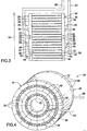
- Exemplary capacitor 20 includes a capacitor body 22 and two end electrodes 24 and 26 which are divided into end segments 28 and 30, respectively. Dividing or segmenting end electrodes 24 and 26 allows the segments to move substantially independently from one another which avoids or reduces instances of thermally induced cracking of the end electrodes.
- Each of segments 28 and 30 are connected with a different portion of capacitor body 22 and are not directly connected to one another with a rigid interface. This allows individual segments 28 and 30 to move with expansion and contraction of the portion of capacitor body 22 to which they are connected without causing cracks to form in end electrodes 24 and 26.
- each segment is connected to a different portion of the capacitor body, each segment is therefore substantially only subject to forces caused by the connected portion of the capacitor body.
- the forces are caused by a relative change in dimension between the segment and the portion of the capacitor body to which it is attached, due to the segment and capacitor body having different coefficient of thermal expansions (CTE).
- CTE coefficient of thermal expansions
- Segments include segment edges 32 and segment faces 34, Figs. 2 and 3 .
- the segment edges 32 of adjacent segments may at least temporarily contact one another, Figs. 1 and 2 . This is not considered to affect the substantially independent nature of the movement of the segments relative to one another.
- Gaps 36 define segment edges 32 between adjacent segments. In other instances, segment edges 32 of adjacent segments 28 or 30 do not contact one another at any temperature, Fig. 3 . In these instances, gap 36 is relatively large.
- Other partially extending gaps 39, Fig. 1 may not be between separate electrode segments, but may instead extend only partially across an electrode segment. Partially extending gap 39 may allow the electrode segment to deform rather than crack when subjected to stress. Other configurations of gaps and segments may also be used for reducing the incidence of thermally induced damage.
- Capacitor body 22 includes internal electrodes or electrically conductive layers 38 and 40 and dielectric material or layers 42 and 44, as shown in Figs. 2 and 3 . Electrically conductive layers 38 and 40 are arranged for producing a capacitance.
- Capacitor body 22 shown in Fig. 1 has a cylindrical or annular shape with two circular ends where end electrodes 24 and 26 are attached to electrically conductive layers 38 and 40, respectively.
- Capacitor body 22, in the present example, defines a cylindrical opening 45.
- the cylindrically or annular shaped capacitor body has generally circular end electrodes 24 and 26 which are defined by a radius 47 that extends from a center point 49.
- a circularly shaped gap 37 can be used with capacitor body 22 where the circular gap is defined by a radius 51 which extends from a center point 53.
- center point 53 can be located at a different position than center point 49 so that circular gap 37 is not concentric with generally circular end electrode 24.
- the non-concentric nature of circular gap 37 prevents the gap from being generally co-linear with electrically conductive layers 38 or 40 for any substantial length which limits the distance that electrical current must flow along a length of electrically conductive layer 38 or 40 before reaching end electrode 24 or 26.
- the body is formed by rolling together two sheets 46 and 48 of metallized film.
- Metallized film 46 and 48 has a film portion which serves as dielectric 42 and 44, respectively, and a metal layer having deposited thereon a thin coating on the film portion and which serves as the electrically conductive layers 38 and 40, respectively.
- the film portion is a type of polymer and the metal is deposited on the polymer by condensing a metal vapor.
- Multiple layers of electrically conductive layers 38 and 40 and dielectric 42 and 44 are displayed in a cross section of cylindrically shaped body 22, as shown in Figs. 2 and 3 , however, every other layer 38 or 40 simply represents additional turns of the sheets 46 and 48, respectively.
- Capacitor body 22, shown in Figs. 2 and 3 increases in radius in the direction of arrow 54.
- the two sheets 46 and 48 are rolled together to form capacitor body 22, in the present example, in such a way that electrically conductive layer 38 extends to a lengthwise edge 50 of sheet 46 and electrically conductive layer 40 extends to a lengthwise edge 52 of sheet 48 as shown in Figs. 2 and 3 . Electrically conductive layers 38 are connected to end segments 28 of end electrode 24 along lengthwise edge 50.
- capacitor body 22 may also be used. For example, separate layers of electrically conductive material and dielectric may be used, and the capacitor body may be formed with a rectangular shape.
- End electrodes 24 and 26 are typically attached to capacitor body 22 by spraying an end spray metal onto the lengthwise edges 50 and 52, respectively.
- the end spray metal is heated to a molten state and droplets of the metal are deposited onto edges 50 and 52 where contact is made with electrically conductive layers 38 and 40, respectively.
- Metals used for the end spray metal include tin, zinc, and/or others.
- the droplets of end spray metal are deposited on capacitor body 22 until the end electrodes are sufficiently thick. In some examples, sufficient thickness occurs when the end electrodes are thick enough to withstand connection of flexible electrical conductors 56 ( Fig. 3 ) at connection points 58 on the faces 34 of the end electrodes 24 and 26. As an example, the thickness of the sprayed electrodes in some capacitors is typically 0.005" to 0.025" thick.
- end electrodes 24 and 26 are segmented or divided by using a mask with the spraying process.
- the mask is placed relative to lengthwise edges 50 and 52 of capacitor body 22 during the spraying process.
- the mask may have metal rods or spokes which block the droplets end spray metal from reaching portions of lengthwise edges 50 and 52 of electrically conductive layers 38 and 40 which leaves gaps 36 in end electrodes 24 and 26. Segments 28 and 30 are formed with the end spray metal where the mask does not block the droplets from contacting lengthwise edges 50 and 52.
- Other materials and masking techniques may be used to create end electrodes 24 and 26 with segments 28 and 30.
- Segments 28 and 30 may also be created by sawing or otherwise cutting the end electrodes 24 and 26 after the end electrodes are connected or formed on capacitor body 22 as solid or undivided pieces.
- a circular saw blade is used to cut gaps 36 in end electrodes 24 and 26 to create the segments 28 and 30.
- Some segments 28 and 30 are divided with an arrangement where at least some gaps 36 run along a radius of a circularly shaped end electrode.
- Other segment patterns or arrangements may also be used so long as the segments reduce the instance of cracking of the end electrodes.
- Some patterns or arrangements of segments may be better at reducing or eliminating thermally induced damage than other patterns or arrangements of segments. This may depend, at least in part, on the directions in which capacitor body 22 expands the greatest when heated. It is considered that one of ordinary skill in the art can accomplish forming segments in a suitable manner such as, for example, by using a mask, sawing or in any other suitable way, with this disclosure in hand.
- the number of segments is based at least partially on the size of end electrodes 24 and 26, in some instances. Larger end electrodes generally require more segments than do small end electrodes. Typically, more segments yield a decreased risk of thermally induced damage than does fewer segments for a given size of end electrode. However, there are practical limits on the number of segments which the end electrodes can be divided into, since it is typically more difficult to attach flexible conductors 56 to smaller segments. As an example, a cylindrical or annular shaped capacitor having an end electrode with a diameter of approximately ten inches, may have 12 to 24 separate electrode segments on each end. These or other end electrodes may have more or less segments, and the number or arrangement of segments on each end electrode of a single capacitor may be different.
- Segments 28 and 30 shown in Fig. 3 are attached to buses 60 and 62 with flexible electrical conductors 56.
- Buses 60 and 62 are relatively rigid and flexible electrical conductors 56, shown in Fig. 3 , are made of bendable metal which allows the segments to move relative to one another without breaking loose from busses 60 and 62.
- Flexible electrical conductors 56 electrically connect segments 28 to buses 60 and electrically connect segments 30 to bus 62.
- Buses 60 and 62 serve as terminals to connect capacitor 20 to other electrical components (not shown).
- Flexible electrical conductors 56 shown in Fig. 4 are made of braided wires. Flexible electrical conductors 56, in this instance, electrically connect adjacent segments 28 to one another and adjacent segments 30 to one another at connection points 58. In this arrangement, all of segments 28 are electrically connected to one another to serve as end electrode 24; and all of the segments 30 are electrically connected to one another to serve as end electrode 26. Flexible cables 64 and 66 serve as terminals to electrically connect each end electrode 24 and 26 of the capacitor 20 to other electrical components.
- each of the segments 28 and 30 can each have independent flexible terminals and/or the segments can be organized in groups which are electrically connected together.
- the terminals are connected together externally to the capacitor.
- the capacitor may have only one end electrode divided into segments.
- connections to segments 28 and 30 should have a flexible nature which does not unduly interfere with the movement of one segment relative to the other segments.
- ESL equivalent series inductance
- Segmenting one or more of the end electrodes improves the reliability of the capacitor by reducing or eliminating the incidences where the capacitor fails or degrades due to thermally induced damage. Affects of CTE mismatch are mitigated by separating the end electrodes into segments which reduces forces acting to damage the end electrodes. The segments reduce or eliminate the effects that expanding portions of one part of the capacitor body have on segments which are not connected to the part of the capacitor body. Segmenting the end electrodes allows the segments to move in different directions and/or at different rates from one another, which reduces the stress between different portions of the end electrodes. Segmented end electrodes can be used on capacitors with a metal or rigid interface between capacitor internal electrode layers and external connections.
- this writing discloses as one exemplary embodiment a capacitor with a segmented end electrode and methods for segmenting an end electrode of a capacitor for reducing or eliminating instances of thermally induced damage of the capacitor.
Landscapes
- Engineering & Computer Science (AREA)
- Power Engineering (AREA)
- Microelectronics & Electronic Packaging (AREA)
- Manufacturing & Machinery (AREA)
- Fixed Capacitors And Capacitor Manufacturing Machines (AREA)
Claims (34)
- Procédé de fabrication d'un condensateur (20) qui résiste à la dégradation induite thermiquement, le procédé comprenant les étapes consistant à :former un corps (22) de condensateur en positionnant une première couche électroconductrice (38) dans une relation espacée par rapport à une seconde couche électroconductrice (40) en plaçant un matériau diélectrique (44) entre les première et seconde couches, ladite première couche (38) ayant un bord longitudinal (50) de première couche au niveau d'une première extrémité dudit corps (22) de condensateur et ladite seconde couche (40) ayant un bord longitudinal (52) de seconde couche au niveau d'une seconde extrémité opposée dudit corps (22) de condensateur ;pulvériser un métal de pulvérisation d'extrémité en contact avec le bord longitudinal (50) de première couche au niveau de la première extrémité du corps (22) de condensateur pour créer une première électrode (24) d'extrémité et pulvériser le métal de pulvérisation d'extrémité en contact avec le bord longitudinal (52) de seconde couche au niveau de la seconde extrémité du corps (22) de condensateur pour créer une seconde électrode (26) d'extrémité, le métal de pulvérisation d'extrémité ayant un coefficient de dilatation thermique qui est différent d'un coefficient de dilatation thermique du matériau diélectrique (44) ;diviser la première électrode (24) d'extrémité en des segments (28) de première électrode qui sont chacun connectés électriquement à différentes parties du bord longitudinal (50) de première couche au niveau de la première extrémité, les segments (28) de première électrode étant disposés pour permettre au matériau diélectrique (44) de se dilater et de se contracter thermiquement tandis que les segments (28) restent connectés électriquement aux différentes parties du bord longitudinal (50) au niveau de la première extrémité ; etconnecter les segments (28) de première électrode à des conducteurs électriques souples (56) pour connecter électriquement les segments (28) de première électrode ensemble tout en permettant aux segments (28) de première électrode de se déplacer sensiblement indépendamment les uns des autres, le condensateur (20) ayant une capacité entre les segments (28) de première électrode connectés et la seconde électrode (26) d'extrémité.
- Procédé selon la revendication 1, comprenant en outre l'étape consistant à :diviser la seconde électrode (26) d'extrémité en des segments (30) de seconde électrode qui sont chacun connectés électriquement à une partie différente du bord longitudinal (52) de seconde couche au niveau de la seconde extrémité pour permettre au matériau diélectrique (44) de se dilater et de se contracter thermiquement tandis que les segments (30) de seconde électrode restent connectés au bord longitudinal (52) de seconde couche ; etconnecter les segments (30) de seconde électrode à des conducteurs électriques souples (56) pour connecter électriquement les segments (30) de seconde électrode ensemble tout en permettant aux segments (30) de seconde électrode de se déplacer sensiblement indépendamment les uns des autres, le condensateur (20) ayant ladite capacité entre les segments (28) de première électrode connectés et les segments (30) de seconde électrode connectés.
- Procédé selon la revendication 1, un film de polymère métallisé étant utilisé pour former les couches électroconductrices (38, 40) et le matériau diélectrique (44).
- Procédé selon la revendication 1, la première électrode (24) d'extrémité étant divisée en segments (28) de première électrode en sciant la première électrode (24) d'extrémité, ou la première électrode (24) d'extrémité étant divisée en segments (28) de première électrode en masquant la première extrémité du corps (22) de condensateur avant de pulvériser le métal de pulvérisation d'extrémité en contact avec le bord longitudinal (50) de première couche.
- Procédé selon la revendication 2, les écarts entre des segments (28) de première électrode directement adjacents comprenant des écarts radiaux (36) et des écarts de forme circulaire (37), et les écarts entre des segments (30) de seconde électrode directement adjacents comprenant des écarts radiaux (36) et des écarts de forme circulaire (37).
- Procédé selon la revendication 5, la première extrémité étant masquée avec un masque en métal qui comprend des barres de métal.
- Procédé selon la revendication 1, les électrodes (24, 26) d'extrémité étant divisées à l'aide d'une pointe tranchante.
- Procédé selon la revendication 1, la première électrode (24) d'extrémité ayant une forme généralement circulaire définie par un premier rayon s'étendant d'un premier point central et les segments (28) de première électrode comprenant une forme circulaire de segment qui est définie par un second rayon s'étendant d'un second point central, les premier et second points centraux se trouvant à différents emplacements.
- Procédé de réduction de la dégradation induite thermiquement dans un condensateur (20) à film métallisé ayant une configuration de première et seconde électrodes internes constituée de couches (38, 40) de film métallisé qui sont isolées électriquement entre elles et la première électrode interne étant connectée électriquement à une première électrode (24) d'extrémité au niveau d'une première extrémité et la seconde électrode interne étant connectée électriquement à une seconde électrode (26) d'extrémité au niveau d'une seconde extrémité, les première (24) et seconde (26) électrodes d'extrémité étant sensiblement rigides et ayant un coefficient de dilatation thermique qui est différent d'un coefficient de dilatation thermique du film métallisé, le procédé comprenant l'étape consistant à :diviser les électrodes (24, 26) d'extrémité en segments (28, 30) d'électrode pour permettre au film métallisé de se dilater et de se contracter thermiquement tandis que la première électrode interne reste connectée électriquement à la première électrode (24) d'extrémité et la seconde électrode interne reste connectée électriquement à la seconde électrode (26) d'extrémité.
- Procédé selon la revendication 9, les électrodes (24, 26) d'extrémité étant divisées en segments (28, 30) en sciant les électrodes (24, 26) d'extrémité après que les électrodes (24, 26) d'extrémité sont pulvérisées sur les électrodes internes dans un état fondu, ou les électrodes (24, 26) d'extrémité étant divisées en segments (28, 30) d'électrode en masquant les extrémités des électrodes internes et en pulvérisant les électrodes (24, 26) d'extrémité en contact avec les électrodes internes sur les extrémités.
- Procédé selon la revendication 9, les écarts entre des segments (28, 30) d'électrode directement adjacents de chaque électrode (24, 26) d'extrémité comprenant des écarts radiaux (36) et des écarts de forme circulaire (37).
- Procédé selon la revendication 11, les segments (28, 30) étant masqués avec un masque en métal qui comprend des barres de métal.
- Procédé selon la revendication 9, les électrodes (24, 26) d'extrémité étant divisées à l'aide d'une pointe tranchante.
- Procédé selon la revendication 9, comprenant en outre les étapes consistant à connecter électriquement les segments (28) d'électrode d'une extrémité (24) ensemble et à connecter électriquement les segments (30) d'électrode de l'autre extrémité (26) ensemble, les segments (28) d'électrode d'une extrémité étant isolés électriquement des segments (30) d'électrode de l'autre extrémité.
- Procédé selon la revendication 9, les films métallisés étant disposés en couches alternées en roulant les films métallisés en une forme généralement cylindrique.
- Procédé, pour la production d'un condensateur (20) avec des électrodes (24, 26) d'extrémité métalliques connectées à un film métallisé (46, 48) enroulé ayant un matériau diélectrique (42, 44) qui se dilate et se contracte thermiquement, comprenant l'étape consistant à :diviser chacune des électrodes (24, 26) d'extrémité en une pluralité de segments (28, 30) d'électrode qui peuvent se déplacer sensiblement indépendamment l'un de l'autre tout en restant connectés au film métallisé (46, 48) en réponse à la contraction et à la dilatation thermiques.
- Procédé selon la revendication 16, comprenant en outre l'étape consistant à :connecter les segments (28, 30) d'électrode de chaque électrode (24, 26) d'extrémité l'un à l'autre électriquement avec un ou plusieurs connecteurs électriques souples, ou connecter les segments (28, 30) d'électrode l'un à l'autre électriquement à l'aide d'un ou de plusieurs connecteurs électriques à câble tressé.
- Procédé selon la revendication 16, les écarts entre des segments (28, 30) d'électrode directement adjacents de chaque électrode (24, 26) d'extrémité comprenant des écarts radiaux (36) et des écarts de forme circulaire (37).
- Procédé selon la revendication 16, les électrodes (24, 26) d'extrémité étant divisées à l'aide d'une pointe tranchante.
- Procédé selon la revendication 16, les électrodes (24, 26) d'extrémité métalliques ayant une forme généralement circulaire définie par un premier rayon s'étendant d'un premier point central et les segments (28) ayant une forme circulaire de segment qui est définie par un second rayon s'étendant d'un second point central, les premier et second points centraux se trouvant à différents emplacements.
- Condensateur (20), comprenant :une première couche électroconductrice (38) ayant un bord longitudinal (50) de première couche ;une seconde couche électroconductrice (40) ayant un bord longitudinal (52) de seconde couche, les première (38) et seconde (40) couches électroconductrices étant disposées dans une relation espacée l'une de l'autre ;un matériau diélectrique (44) placé entre les première (38) et seconde (40) couches électroconductrices ;une première électrode (24) d'extrémité qui est connectée électriquement au bord longitudinal (50) de première couche ; etune seconde électrode (26) d'extrémité qui est connectée électriquement au bord longitudinal (52) de seconde couche, la seconde électrode (26) d'extrémité étant divisée en plusieurs segments (30) d'électrode qui sont chacun connectés à différentes parties du bord longitudinal (52) de seconde couche, le matériau diélectrique (44) pouvant se dilater et se contracter thermiquement tandis que les segments (30) d'électrode restent connectés au bord longitudinal (52) de seconde couche et le condensateur (20) ayant une capacité entre chacun des segments (30) d'électrode et la première électrode (24) d'extrémité.
- Condensateur (20) selon la revendication 21, les segments (30) d'électrode susmentionnés étant des segments (30) de seconde électrode et la première électrode (24) d'extrémité étant divisée en une pluralité de segments (28) de première électrode qui sont chacun connectés à des parties différentes du bord longitudinal (50) de première couche, le matériau diélectrique (44) pouvant se dilater thermiquement.
- Condensateur (20) selon la revendication 21, les première (38) et seconde (40) couches électroconductrices étant chacune des parties de feuilles uniques de polymère métallisé qui sont roulées ensemble en une forme généralement cylindrique.
- Condensateur (20) selon la revendication 23, la seconde électrode (26) d'extrémité ayant une forme généralement circulaire et les segments (30) d'électrode étant définis par des écarts (39) qui sont positionnés au moins partiellement sur un rayon de la forme circulaire.
- Condensateur (20) selon la revendication 23, la seconde électrode (26) d'extrémité ayant une forme généralement circulaire et le nombre de segments (30) d'électrode dépendant du rayon de la forme circulaire.
- Condensateur (20) selon la revendication 25, la forme circulaire de la seconde électrode (26) d'extrémité ayant un diamètre d'environ 10 pouces et le nombre de segments (30) d'électrode étant de l'ordre de 12 à 24.
- Condensateur (20) selon la revendication 21, le nombre de segments (30) d'électrode dépendant d'une dimension de la seconde électrode (26) d'extrémité.
- Condensateur (20) selon la revendication 21, les segments (30) d'électrode étant divisés de sorte à optimiser une résistance à la fissuration induite thermiquement de la seconde électrode (26) d'extrémité.
- Condensateur (20) selon la revendication 21, au moins deux des segments (30) d'électrode étant connectés ensemble avec un conducteur souple (56).
- Condensateur (20) selon la revendication 29, le conducteur souple (56) étant un fil tressé, ou le conducteur souple (56) étant une bande métallique souple.
- Condensateur (20) selon la revendication de 21, les écarts entre la pluralité des segments (28) d'électrode de la première électrode (24) d'extrémité comprenant des écarts radiaux (36) et des écarts de forme circulaire (37), et les écarts entre la pluralité des segments (30) d'électrode de la seconde électrode (26) d'extrémité comprenant des écarts radiaux (36) et des écarts de forme circulaire (37).
- Condensateur (20) selon la revendication 21, chacun des segments (30) d'électrode étant connecté à un terminal électrique séparé.
- Condensateur (20) selon la revendication 21, la seconde électrode (26) d'extrémité ayant une forme généralement circulaire définie par un premier rayon s'étendant d'un premier point central et les segments d'électrode comprenant une forme circulaire de segment qui est définie par un second rayon s'étendant d'un second point central, les premier et second points centraux se trouvant à différents emplacements.
- Condensateur (20) selon la revendication 21, au moins un segment (30) d'électrode donné comprenant un écart (39) qui s'étend partiellement sur le segment d'électrode donné.
Applications Claiming Priority (3)
| Application Number | Priority Date | Filing Date | Title |
|---|---|---|---|
| US59578305P | 2005-08-05 | 2005-08-05 | |
| US11/495,447 US7453114B2 (en) | 2005-08-05 | 2006-07-28 | Segmented end electrode capacitor and method of segmenting an end electrode of a capacitor |
| PCT/US2006/030593 WO2007019383A1 (fr) | 2005-08-05 | 2006-08-03 | Condensateur resistif avec degradation induite thermiquement et procede |
Publications (3)
| Publication Number | Publication Date |
|---|---|
| EP1913609A1 EP1913609A1 (fr) | 2008-04-23 |
| EP1913609A4 EP1913609A4 (fr) | 2012-04-25 |
| EP1913609B1 true EP1913609B1 (fr) | 2016-04-13 |
Family
ID=37717425
Family Applications (1)
| Application Number | Title | Priority Date | Filing Date |
|---|---|---|---|
| EP06800829.1A Active EP1913609B1 (fr) | 2005-08-05 | 2006-08-03 | Condensateur resistif avec degradation induite thermiquement et procede |
Country Status (9)
| Country | Link |
|---|---|
| US (2) | US7453114B2 (fr) |
| EP (1) | EP1913609B1 (fr) |
| JP (1) | JP5060481B2 (fr) |
| KR (1) | KR101271436B1 (fr) |
| CN (1) | CN101258568B (fr) |
| BR (1) | BRPI0614704A2 (fr) |
| CA (1) | CA2617785C (fr) |
| IL (1) | IL189223A (fr) |
| WO (1) | WO2007019383A1 (fr) |
Families Citing this family (39)
| Publication number | Priority date | Publication date | Assignee | Title |
|---|---|---|---|---|
| US8064188B2 (en) | 2000-07-20 | 2011-11-22 | Paratek Microwave, Inc. | Optimized thin film capacitors |
| US8744384B2 (en) | 2000-07-20 | 2014-06-03 | Blackberry Limited | Tunable microwave devices with auto-adjusting matching circuit |
| US7869186B2 (en) * | 2005-11-14 | 2011-01-11 | Paratek Microwave, Inc. | High Q and low stress capacitor electrode array |
| US9406444B2 (en) | 2005-11-14 | 2016-08-02 | Blackberry Limited | Thin film capacitors |
| US7711337B2 (en) | 2006-01-14 | 2010-05-04 | Paratek Microwave, Inc. | Adaptive impedance matching module (AIMM) control architectures |
| US7714676B2 (en) | 2006-11-08 | 2010-05-11 | Paratek Microwave, Inc. | Adaptive impedance matching apparatus, system and method |
| US7535312B2 (en) | 2006-11-08 | 2009-05-19 | Paratek Microwave, Inc. | Adaptive impedance matching apparatus, system and method with improved dynamic range |
| US7917104B2 (en) * | 2007-04-23 | 2011-03-29 | Paratek Microwave, Inc. | Techniques for improved adaptive impedance matching |
| US8213886B2 (en) | 2007-05-07 | 2012-07-03 | Paratek Microwave, Inc. | Hybrid techniques for antenna retuning utilizing transmit and receive power information |
| US7991363B2 (en) | 2007-11-14 | 2011-08-02 | Paratek Microwave, Inc. | Tuning matching circuits for transmitter and receiver bands as a function of transmitter metrics |
| US8072285B2 (en) | 2008-09-24 | 2011-12-06 | Paratek Microwave, Inc. | Methods for tuning an adaptive impedance matching network with a look-up table |
| WO2010137632A1 (fr) | 2009-05-26 | 2010-12-02 | 帝人化成株式会社 | Composition de résine ignifuge et article moulé a partir de celle-ci |
| US8451133B2 (en) * | 2009-08-07 | 2013-05-28 | Electronic Concepts, Inc. | Large current carrying capacitor having a thermal disconnect with a light indicator |
| US8472888B2 (en) | 2009-08-25 | 2013-06-25 | Research In Motion Rf, Inc. | Method and apparatus for calibrating a communication device |
| US9026062B2 (en) | 2009-10-10 | 2015-05-05 | Blackberry Limited | Method and apparatus for managing operations of a communication device |
| US8803631B2 (en) | 2010-03-22 | 2014-08-12 | Blackberry Limited | Method and apparatus for adapting a variable impedance network |
| WO2011133657A2 (fr) | 2010-04-20 | 2011-10-27 | Paratek Microwave, Inc. | Procédé et appareil permettant de gérer l'interférence dans un dispositif de communication |
| US9379454B2 (en) | 2010-11-08 | 2016-06-28 | Blackberry Limited | Method and apparatus for tuning antennas in a communication device |
| US8712340B2 (en) | 2011-02-18 | 2014-04-29 | Blackberry Limited | Method and apparatus for radio antenna frequency tuning |
| US8655286B2 (en) | 2011-02-25 | 2014-02-18 | Blackberry Limited | Method and apparatus for tuning a communication device |
| US8594584B2 (en) | 2011-05-16 | 2013-11-26 | Blackberry Limited | Method and apparatus for tuning a communication device |
| WO2013022826A1 (fr) | 2011-08-05 | 2013-02-14 | Research In Motion Rf, Inc. | Procédé et appareil pour un réglage de bande dans un dispositif de communication |
| US8948889B2 (en) | 2012-06-01 | 2015-02-03 | Blackberry Limited | Methods and apparatus for tuning circuit components of a communication device |
| US9350405B2 (en) | 2012-07-19 | 2016-05-24 | Blackberry Limited | Method and apparatus for antenna tuning and power consumption management in a communication device |
| MX2014004923A (es) * | 2012-07-27 | 2014-10-17 | Rtr En S L | Condensador trifasico formado por dos cilindros alineados con desconexion por sobre presion. |
| US10404295B2 (en) | 2012-12-21 | 2019-09-03 | Blackberry Limited | Method and apparatus for adjusting the timing of radio antenna tuning |
| US9374113B2 (en) | 2012-12-21 | 2016-06-21 | Blackberry Limited | Method and apparatus for adjusting the timing of radio antenna tuning |
| US20140226259A1 (en) * | 2013-02-13 | 2014-08-14 | Sbe, Inc. | Mitigating the Effects of Cracks in Metallized Polymer Film Capacitor Arc-Sprayed End Connections |
| EP2983183A1 (fr) * | 2014-08-07 | 2016-02-10 | Siemens Aktiengesellschaft | Condensateur à film pour pression ambiante élevée |
| JP6458444B2 (ja) * | 2014-10-21 | 2019-01-30 | 株式会社デンソー | 電力変換装置 |
| US9831035B2 (en) * | 2014-10-31 | 2017-11-28 | Deere & Company | Capacitor with improved heat dissipation |
| US9438319B2 (en) | 2014-12-16 | 2016-09-06 | Blackberry Limited | Method and apparatus for antenna selection |
| US9722531B2 (en) | 2015-05-22 | 2017-08-01 | Deere & Company | Electronic inverter assembly with an integral snubber capacitor |
| US9490555B1 (en) * | 2015-05-22 | 2016-11-08 | Deere & Company | System or connector for voltage bus structures |
| US9979320B2 (en) | 2016-08-26 | 2018-05-22 | Deere & Company | Electronic inverter assembly |
| CN110763357A (zh) * | 2019-11-08 | 2020-02-07 | 江苏科技大学 | 一种电容式温度传感器及使用方法 |
| CN114914089A (zh) * | 2021-02-08 | 2022-08-16 | 日月光半导体制造股份有限公司 | 电容器结构 |
| CN113555225B (zh) * | 2021-07-22 | 2023-04-07 | 广州巨湾技研有限公司 | 一种管式多层结构超级电容器及其制备方法 |
| DE102024205056A1 (de) * | 2024-05-31 | 2025-12-04 | Robert Bosch Gesellschaft mit beschränkter Haftung | Folienkondensator |
Family Cites Families (15)
| Publication number | Priority date | Publication date | Assignee | Title |
|---|---|---|---|---|
| JPS59144117A (ja) * | 1983-02-07 | 1984-08-18 | 松下電器産業株式会社 | フイルムコンデンサの電極装置 |
| JPS59215715A (ja) * | 1983-05-23 | 1984-12-05 | マルコン電子株式会社 | 積層形フイルムコンデンサの製造方法 |
| JPS6194332U (fr) * | 1984-11-26 | 1986-06-18 | ||
| ATE78950T1 (de) * | 1987-07-31 | 1992-08-15 | Siemens Ag | Fuellschichtbauteil mit einem gesinterten, monolithischen keramikkoerper und verfahren zu dessen herstellung. |
| JPH0770425B2 (ja) * | 1987-09-18 | 1995-07-31 | 松下電器産業株式会社 | コンデンサの製造方法 |
| JPH02121320A (ja) * | 1988-10-29 | 1990-05-09 | Matsushita Electric Ind Co Ltd | 複合金属化コンデンサ |
| JPH0888144A (ja) * | 1994-09-14 | 1996-04-02 | Nitsuko Corp | チップ形フィルムコンデンサ |
| US6191933B1 (en) * | 1998-01-07 | 2001-02-20 | Tdk Corporation | Ceramic capacitor |
| JP2001076966A (ja) * | 1999-09-08 | 2001-03-23 | Soshin Electric Co Ltd | 油含浸型フィルムコンデンサ。 |
| JP2001126948A (ja) * | 1999-11-01 | 2001-05-11 | Soshin Electric Co Ltd | 水冷式フィルムコンデンサ。 |
| SE515930C2 (sv) * | 2000-01-26 | 2001-10-29 | Abb Ab | Kondensator och förfarande för att vid ett kondensatorelement elektriskt sammanbinda elektrodskikt med en anslutningspunkt |
| JP2002057063A (ja) * | 2000-08-11 | 2002-02-22 | Murata Mfg Co Ltd | 積層セラミック電子部品 |
| US6605551B2 (en) * | 2000-12-08 | 2003-08-12 | Intel Corporation | Electrocoating process to form a dielectric layer in an organic substrate to reduce loop inductance |
| US6477035B1 (en) * | 2001-10-10 | 2002-11-05 | Lockheed Martin Corporation | Integrally formed energy storage device and method of fabrication |
| JP2005136132A (ja) * | 2003-10-30 | 2005-05-26 | Tdk Corp | 積層コンデンサ |
-
2006
- 2006-07-28 US US11/495,447 patent/US7453114B2/en active Active
- 2006-08-03 JP JP2008525255A patent/JP5060481B2/ja not_active Expired - Fee Related
- 2006-08-03 CN CN2006800324945A patent/CN101258568B/zh not_active Expired - Fee Related
- 2006-08-03 WO PCT/US2006/030593 patent/WO2007019383A1/fr not_active Ceased
- 2006-08-03 BR BRPI0614704-6A patent/BRPI0614704A2/pt not_active IP Right Cessation
- 2006-08-03 EP EP06800829.1A patent/EP1913609B1/fr active Active
- 2006-08-03 CA CA2617785A patent/CA2617785C/fr not_active Expired - Fee Related
- 2006-08-03 KR KR1020087003001A patent/KR101271436B1/ko not_active Expired - Fee Related
-
2008
- 2008-02-03 IL IL189223A patent/IL189223A/en not_active IP Right Cessation
- 2008-10-01 US US12/243,777 patent/US7655530B2/en active Active
Also Published As
| Publication number | Publication date |
|---|---|
| JP2009503911A (ja) | 2009-01-29 |
| EP1913609A4 (fr) | 2012-04-25 |
| JP5060481B2 (ja) | 2012-10-31 |
| IL189223A (en) | 2012-06-28 |
| EP1913609A1 (fr) | 2008-04-23 |
| WO2007019383A9 (fr) | 2008-07-17 |
| CA2617785C (fr) | 2014-05-06 |
| US7453114B2 (en) | 2008-11-18 |
| KR101271436B1 (ko) | 2013-06-05 |
| CN101258568A (zh) | 2008-09-03 |
| CA2617785A1 (fr) | 2007-02-15 |
| IL189223A0 (en) | 2008-11-03 |
| BRPI0614704A2 (pt) | 2011-08-30 |
| US7655530B2 (en) | 2010-02-02 |
| US20070030624A1 (en) | 2007-02-08 |
| KR20080031943A (ko) | 2008-04-11 |
| US20090031543A1 (en) | 2009-02-05 |
| WO2007019383A1 (fr) | 2007-02-15 |
| CN101258568B (zh) | 2011-03-23 |
Similar Documents
| Publication | Publication Date | Title |
|---|---|---|
| EP1913609B1 (fr) | Condensateur resistif avec degradation induite thermiquement et procede | |
| US20160087409A1 (en) | Devices and methods related to gas discharge tubes | |
| US20080232024A1 (en) | Metalized plastic film for film capacitor and film capacitor | |
| CN111341509A (zh) | 一种抗硫化芯片电阻器及其制造方法 | |
| JP2005012082A (ja) | 金属化フィルムコンデンサ | |
| JP4698474B2 (ja) | フィルムコンデンサ | |
| US10115523B2 (en) | Ceramic electronic component and mounting structure of the same | |
| EP1868216A1 (fr) | Condensateur metallise et condensateur de lissage d'onduleur pour automobile | |
| SE515894C2 (sv) | Kondensatorelement för en kraftkondensator, kraftkondensator innefattande dylikt kondensatorelement samt metalliserat band för en kraftkondensator | |
| CN107275084A (zh) | 金属化薄膜电容器及其制造方法以及金属化薄膜层叠体 | |
| SE515930C2 (sv) | Kondensator och förfarande för att vid ett kondensatorelement elektriskt sammanbinda elektrodskikt med en anslutningspunkt | |
| CN1327242A (zh) | 电阻器及其制造方法 | |
| KR100913943B1 (ko) | 금속화 플라스틱 필름 및 필름커패시터 | |
| JP2006286988A (ja) | 金属化フィルムコンデンサ | |
| JP2001110601A (ja) | 抵抗器およびその製造方法 | |
| US20140226259A1 (en) | Mitigating the Effects of Cracks in Metallized Polymer Film Capacitor Arc-Sprayed End Connections | |
| JPH09283366A (ja) | コンデンサ | |
| CN101548347A (zh) | 防静电部件以及其制造方法 | |
| CN223598484U (zh) | 耐电性薄膜电阻结构 | |
| CN119943515B (zh) | 晶片电阻 | |
| US20230420204A1 (en) | Thermal fuse | |
| JP2737896B2 (ja) | 保安機能付きコンデンサ用金属化基体 | |
| KR200393101Y1 (ko) | 필름 커패시터용 금속화 플라스틱필름 | |
| TWM668138U (zh) | 耐電性薄膜電阻結構 | |
| CN119480305A (zh) | 金属氧化物-聚苯胺聚合物基质压敏电阻 |
Legal Events
| Date | Code | Title | Description |
|---|---|---|---|
| PUAI | Public reference made under article 153(3) epc to a published international application that has entered the european phase |
Free format text: ORIGINAL CODE: 0009012 |
|
| 17P | Request for examination filed |
Effective date: 20080229 |
|
| AK | Designated contracting states |
Kind code of ref document: A1 Designated state(s): AT BE BG CH CY CZ DE DK EE ES FI FR GB GR HU IE IS IT LI LT LU LV MC NL PL PT RO SE SI SK TR |
|
| REG | Reference to a national code |
Ref country code: DE Ref legal event code: R079 Ref document number: 602006048705 Country of ref document: DE Free format text: PREVIOUS MAIN CLASS: H01G0004300000 Ipc: H01G0004232000 |
|
| A4 | Supplementary search report drawn up and despatched |
Effective date: 20120322 |
|
| RIC1 | Information provided on ipc code assigned before grant |
Ipc: H01G 4/32 20060101ALI20120316BHEP Ipc: H01G 4/232 20060101AFI20120316BHEP Ipc: H01G 4/30 20060101ALI20120316BHEP |
|
| DAX | Request for extension of the european patent (deleted) | ||
| GRAP | Despatch of communication of intention to grant a patent |
Free format text: ORIGINAL CODE: EPIDOSNIGR1 |
|
| INTG | Intention to grant announced |
Effective date: 20151125 |
|
| GRAS | Grant fee paid |
Free format text: ORIGINAL CODE: EPIDOSNIGR3 |
|
| GRAA | (expected) grant |
Free format text: ORIGINAL CODE: 0009210 |
|
| AK | Designated contracting states |
Kind code of ref document: B1 Designated state(s): AT BE BG CH CY CZ DE DK EE ES FI FR GB GR HU IE IS IT LI LT LU LV MC NL PL PT RO SE SI SK TR |
|
| REG | Reference to a national code |
Ref country code: GB Ref legal event code: FG4D |
|
| REG | Reference to a national code |
Ref country code: AT Ref legal event code: REF Ref document number: 790921 Country of ref document: AT Kind code of ref document: T Effective date: 20160415 Ref country code: CH Ref legal event code: EP |
|
| REG | Reference to a national code |
Ref country code: IE Ref legal event code: FG4D |
|
| REG | Reference to a national code |
Ref country code: DE Ref legal event code: R096 Ref document number: 602006048705 Country of ref document: DE |
|
| REG | Reference to a national code |
Ref country code: FR Ref legal event code: PLFP Year of fee payment: 11 |
|
| REG | Reference to a national code |
Ref country code: LT Ref legal event code: MG4D |
|
| REG | Reference to a national code |
Ref country code: AT Ref legal event code: MK05 Ref document number: 790921 Country of ref document: AT Kind code of ref document: T Effective date: 20160413 |
|
| REG | Reference to a national code |
Ref country code: NL Ref legal event code: MP Effective date: 20160413 |
|
| PG25 | Lapsed in a contracting state [announced via postgrant information from national office to epo] |
Ref country code: LT Free format text: LAPSE BECAUSE OF FAILURE TO SUBMIT A TRANSLATION OF THE DESCRIPTION OR TO PAY THE FEE WITHIN THE PRESCRIBED TIME-LIMIT Effective date: 20160413 Ref country code: PL Free format text: LAPSE BECAUSE OF FAILURE TO SUBMIT A TRANSLATION OF THE DESCRIPTION OR TO PAY THE FEE WITHIN THE PRESCRIBED TIME-LIMIT Effective date: 20160413 Ref country code: FI Free format text: LAPSE BECAUSE OF FAILURE TO SUBMIT A TRANSLATION OF THE DESCRIPTION OR TO PAY THE FEE WITHIN THE PRESCRIBED TIME-LIMIT Effective date: 20160413 Ref country code: NL Free format text: LAPSE BECAUSE OF FAILURE TO SUBMIT A TRANSLATION OF THE DESCRIPTION OR TO PAY THE FEE WITHIN THE PRESCRIBED TIME-LIMIT Effective date: 20160413 |
|
| PG25 | Lapsed in a contracting state [announced via postgrant information from national office to epo] |
Ref country code: GR Free format text: LAPSE BECAUSE OF FAILURE TO SUBMIT A TRANSLATION OF THE DESCRIPTION OR TO PAY THE FEE WITHIN THE PRESCRIBED TIME-LIMIT Effective date: 20160714 Ref country code: PT Free format text: LAPSE BECAUSE OF FAILURE TO SUBMIT A TRANSLATION OF THE DESCRIPTION OR TO PAY THE FEE WITHIN THE PRESCRIBED TIME-LIMIT Effective date: 20160816 Ref country code: LV Free format text: LAPSE BECAUSE OF FAILURE TO SUBMIT A TRANSLATION OF THE DESCRIPTION OR TO PAY THE FEE WITHIN THE PRESCRIBED TIME-LIMIT Effective date: 20160413 Ref country code: AT Free format text: LAPSE BECAUSE OF FAILURE TO SUBMIT A TRANSLATION OF THE DESCRIPTION OR TO PAY THE FEE WITHIN THE PRESCRIBED TIME-LIMIT Effective date: 20160413 Ref country code: ES Free format text: LAPSE BECAUSE OF FAILURE TO SUBMIT A TRANSLATION OF THE DESCRIPTION OR TO PAY THE FEE WITHIN THE PRESCRIBED TIME-LIMIT Effective date: 20160413 Ref country code: SE Free format text: LAPSE BECAUSE OF FAILURE TO SUBMIT A TRANSLATION OF THE DESCRIPTION OR TO PAY THE FEE WITHIN THE PRESCRIBED TIME-LIMIT Effective date: 20160413 |
|
| PG25 | Lapsed in a contracting state [announced via postgrant information from national office to epo] |
Ref country code: BE Free format text: LAPSE BECAUSE OF FAILURE TO SUBMIT A TRANSLATION OF THE DESCRIPTION OR TO PAY THE FEE WITHIN THE PRESCRIBED TIME-LIMIT Effective date: 20160413 |
|
| REG | Reference to a national code |
Ref country code: DE Ref legal event code: R097 Ref document number: 602006048705 Country of ref document: DE |
|
| PG25 | Lapsed in a contracting state [announced via postgrant information from national office to epo] |
Ref country code: SK Free format text: LAPSE BECAUSE OF FAILURE TO SUBMIT A TRANSLATION OF THE DESCRIPTION OR TO PAY THE FEE WITHIN THE PRESCRIBED TIME-LIMIT Effective date: 20160413 Ref country code: EE Free format text: LAPSE BECAUSE OF FAILURE TO SUBMIT A TRANSLATION OF THE DESCRIPTION OR TO PAY THE FEE WITHIN THE PRESCRIBED TIME-LIMIT Effective date: 20160413 Ref country code: CZ Free format text: LAPSE BECAUSE OF FAILURE TO SUBMIT A TRANSLATION OF THE DESCRIPTION OR TO PAY THE FEE WITHIN THE PRESCRIBED TIME-LIMIT Effective date: 20160413 Ref country code: DK Free format text: LAPSE BECAUSE OF FAILURE TO SUBMIT A TRANSLATION OF THE DESCRIPTION OR TO PAY THE FEE WITHIN THE PRESCRIBED TIME-LIMIT Effective date: 20160413 Ref country code: RO Free format text: LAPSE BECAUSE OF FAILURE TO SUBMIT A TRANSLATION OF THE DESCRIPTION OR TO PAY THE FEE WITHIN THE PRESCRIBED TIME-LIMIT Effective date: 20160413 |
|
| PLBE | No opposition filed within time limit |
Free format text: ORIGINAL CODE: 0009261 |
|
| STAA | Information on the status of an ep patent application or granted ep patent |
Free format text: STATUS: NO OPPOSITION FILED WITHIN TIME LIMIT |
|
| 26N | No opposition filed |
Effective date: 20170116 |
|
| PG25 | Lapsed in a contracting state [announced via postgrant information from national office to epo] |
Ref country code: MC Free format text: LAPSE BECAUSE OF FAILURE TO SUBMIT A TRANSLATION OF THE DESCRIPTION OR TO PAY THE FEE WITHIN THE PRESCRIBED TIME-LIMIT Effective date: 20160413 |
|
| REG | Reference to a national code |
Ref country code: CH Ref legal event code: PL |
|
| PG25 | Lapsed in a contracting state [announced via postgrant information from national office to epo] |
Ref country code: CH Free format text: LAPSE BECAUSE OF NON-PAYMENT OF DUE FEES Effective date: 20160831 Ref country code: LI Free format text: LAPSE BECAUSE OF NON-PAYMENT OF DUE FEES Effective date: 20160831 |
|
| PG25 | Lapsed in a contracting state [announced via postgrant information from national office to epo] |
Ref country code: SI Free format text: LAPSE BECAUSE OF FAILURE TO SUBMIT A TRANSLATION OF THE DESCRIPTION OR TO PAY THE FEE WITHIN THE PRESCRIBED TIME-LIMIT Effective date: 20160413 |
|
| REG | Reference to a national code |
Ref country code: FR Ref legal event code: PLFP Year of fee payment: 12 |
|
| PG25 | Lapsed in a contracting state [announced via postgrant information from national office to epo] |
Ref country code: LU Free format text: LAPSE BECAUSE OF NON-PAYMENT OF DUE FEES Effective date: 20160803 |
|
| PG25 | Lapsed in a contracting state [announced via postgrant information from national office to epo] |
Ref country code: HU Free format text: LAPSE BECAUSE OF FAILURE TO SUBMIT A TRANSLATION OF THE DESCRIPTION OR TO PAY THE FEE WITHIN THE PRESCRIBED TIME-LIMIT; INVALID AB INITIO Effective date: 20060803 Ref country code: CY Free format text: LAPSE BECAUSE OF FAILURE TO SUBMIT A TRANSLATION OF THE DESCRIPTION OR TO PAY THE FEE WITHIN THE PRESCRIBED TIME-LIMIT Effective date: 20160413 |
|
| REG | Reference to a national code |
Ref country code: FR Ref legal event code: PLFP Year of fee payment: 13 |
|
| PG25 | Lapsed in a contracting state [announced via postgrant information from national office to epo] |
Ref country code: IS Free format text: LAPSE BECAUSE OF FAILURE TO SUBMIT A TRANSLATION OF THE DESCRIPTION OR TO PAY THE FEE WITHIN THE PRESCRIBED TIME-LIMIT Effective date: 20160413 Ref country code: TR Free format text: LAPSE BECAUSE OF FAILURE TO SUBMIT A TRANSLATION OF THE DESCRIPTION OR TO PAY THE FEE WITHIN THE PRESCRIBED TIME-LIMIT Effective date: 20160413 |
|
| PG25 | Lapsed in a contracting state [announced via postgrant information from national office to epo] |
Ref country code: BG Free format text: LAPSE BECAUSE OF FAILURE TO SUBMIT A TRANSLATION OF THE DESCRIPTION OR TO PAY THE FEE WITHIN THE PRESCRIBED TIME-LIMIT Effective date: 20160413 |
|
| PG25 | Lapsed in a contracting state [announced via postgrant information from national office to epo] |
Ref country code: IE Free format text: LAPSE BECAUSE OF NON-PAYMENT OF DUE FEES Effective date: 20190803 |
|
| PGFP | Annual fee paid to national office [announced via postgrant information from national office to epo] |
Ref country code: IT Payment date: 20240710 Year of fee payment: 19 |
|
| PGFP | Annual fee paid to national office [announced via postgrant information from national office to epo] |
Ref country code: GB Payment date: 20250612 Year of fee payment: 20 |
|
| PGFP | Annual fee paid to national office [announced via postgrant information from national office to epo] |
Ref country code: FR Payment date: 20250610 Year of fee payment: 20 |
|
| PGFP | Annual fee paid to national office [announced via postgrant information from national office to epo] |
Ref country code: DE Payment date: 20250611 Year of fee payment: 20 |