EP1936514A1 - Dispositif de traitement de fonctionnement - Google Patents
Dispositif de traitement de fonctionnement Download PDFInfo
- Publication number
- EP1936514A1 EP1936514A1 EP05816411A EP05816411A EP1936514A1 EP 1936514 A1 EP1936514 A1 EP 1936514A1 EP 05816411 A EP05816411 A EP 05816411A EP 05816411 A EP05816411 A EP 05816411A EP 1936514 A1 EP1936514 A1 EP 1936514A1
- Authority
- EP
- European Patent Office
- Prior art keywords
- cross call
- unit
- processor apparatus
- transmission
- identification
- Prior art date
- Legal status (The legal status is an assumption and is not a legal conclusion. Google has not performed a legal analysis and makes no representation as to the accuracy of the status listed.)
- Granted
Links
Images







Classifications
-
- G—PHYSICS
- G06—COMPUTING OR CALCULATING; COUNTING
- G06F—ELECTRIC DIGITAL DATA PROCESSING
- G06F15/00—Digital computers in general; Data processing equipment in general
- G06F15/16—Combinations of two or more digital computers each having at least an arithmetic unit, a program unit and a register, e.g. for a simultaneous processing of several programs
- G06F15/163—Interprocessor communication
- G06F15/17—Interprocessor communication using an input/output type connection, e.g. channel, I/O port
-
- G—PHYSICS
- G06—COMPUTING OR CALCULATING; COUNTING
- G06F—ELECTRIC DIGITAL DATA PROCESSING
- G06F9/00—Arrangements for program control, e.g. control units
- G06F9/06—Arrangements for program control, e.g. control units using stored programs, i.e. using an internal store of processing equipment to receive or retain programs
- G06F9/46—Multiprogramming arrangements
- G06F9/48—Program initiating; Program switching, e.g. by interrupt
- G06F9/4806—Task transfer initiation or dispatching
- G06F9/4812—Task transfer initiation or dispatching by interrupt, e.g. masked
-
- G—PHYSICS
- G06—COMPUTING OR CALCULATING; COUNTING
- G06F—ELECTRIC DIGITAL DATA PROCESSING
- G06F13/00—Interconnection of, or transfer of information or other signals between, memories, input/output devices or central processing units
- G06F13/10—Program control for peripheral devices
-
- G—PHYSICS
- G06—COMPUTING OR CALCULATING; COUNTING
- G06F—ELECTRIC DIGITAL DATA PROCESSING
- G06F9/00—Arrangements for program control, e.g. control units
- G06F9/06—Arrangements for program control, e.g. control units using stored programs, i.e. using an internal store of processing equipment to receive or retain programs
- G06F9/30—Arrangements for executing machine instructions, e.g. instruction decode
-
- G—PHYSICS
- G06—COMPUTING OR CALCULATING; COUNTING
- G06F—ELECTRIC DIGITAL DATA PROCESSING
- G06F9/00—Arrangements for program control, e.g. control units
- G06F9/06—Arrangements for program control, e.g. control units using stored programs, i.e. using an internal store of processing equipment to receive or retain programs
- G06F9/46—Multiprogramming arrangements
- G06F9/50—Allocation of resources, e.g. of the central processing unit [CPU]
Definitions
- the present invention relates to a control technology within an operation processor apparatus such as a CPU, and particularly relates to a control technology for a cross call between the operation processor apparatuses.
- the present invention is related to a cross call between CPUs, and is particularly intended to multi-CPU systems.
- the cross call is one of communication means between processors, and is an internal processor interrupt used by an OS to maintain memory consistency in virtual memory.
- Technologies relating to the present invention include a technology disclosed in Patent Document 1 as an example to prevent a slow-response I/O read from occupying a read management table by separating and controlling memory read and management tables of I/O in a read control apparatus of computer systems employing a read-split technique that is a technique to release a system bus, until a response to a read request is returned to the request issue source.
- Patent Document 2 discloses a technology for the purpose of speeding up a common system bus to provide a versatile interface with a buffer function for connecting plural data processors, memory units and I/O interfaces to the system bus.
- FIG. 1 shows overview of a configuration example of a multi-CPU system.
- a CPUA 1100, a CPUB 1200, and memory 1400 are connected to a system controller (hereinafter referred to as "SC") 1300.
- SC system controller
- each of CPU core units 1110 and 1210 provided in the CPUA 1100 and the CPUB 1200, respectively, are connected to the SC 1300 via external interface units 1120 and 1220, respectively.
- Each of the external interface units 1120 and 1220 has one of cross call send controller (hereinafter referred to as "XCSC” (Cross Call Send Controller)) 1121 and 1221, respectively, and each of cross call receive controller (hereinafter referred to as "XCRC” (Cross Call Receive Controller)) 1122 and 1222.
- XCSC Cross Call Send Controller
- XCRC Cross Call Receive Controller
- FIG. 1 A flow of cross call transmission/reception in the system shown in Fig. 1 is explained with reference to Fig. 2 .
- cross call data (a bold arrow) and an issue request of a cross call request (a thin arrow) are transmitted from the CPU core unit 1110 of the CPUA 1100, as shown by two arrows assigned with (1)
- the XCSC 1121 while buffering the data and the request, issues a cross call request (cross call request) to the SC 1300 as shown by an arrow assigned with (2).
- the CPUA 1100 when receiving the ACK, transmits the cross call data to the SC 1300 as shown by an arrow assigned with (4).
- the CPUA 1100 causes the XCSC 1121 to reissue a cross call request to the SC 1300 after a prescribed time period, and later, repeatedly causes the XCSC 1121 to issue the cross call request until the ACK is received.
- the XCRC 1222 of the CPUB 1200 that is a receiver of the cross call, when receiving the cross call data transmitted from the SC 1300 as indicated by an arrow assigned with (5), writes the data in the internal register.
- the XCRC 1222 transmits a cross call reception notice (a thin arrow pointing outward) to the CPU core unit 1210 of the CPUB 1200 and passes the data (a bold arrow) at the same time as indicated by arrows assigned with (6).
- the XCRC 1222 issues to the SC 1300 a request to clear the BUSY bit indicating the state of the CPUB 1200, as indicated by an arrow assigned with (7) .
- a period of time from the issue of the cross call request (cross call request) from the CPUA to the SC indicated by the arrow of (2) to cancellation of the BUSY state by the CPUB to the SC indicated by the arrow of (7) is a BUSY period in the SC (indicated by an arrow above BUSY).
- Each of the XCSC 1121 and 1221 has a data register, a status register for storing the cross call BUSY state (a cross call being issued) and the cross call NACK state (a cross call issue failed), and a command FIFO for storing the order of command issue and issued contents.
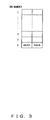
- An example of the structure of the status register is shown in Fig. 3
- an example of the structure of the command FIFO is shown in Fig. 4 .
- the status register keeps and manages the BUSY state and the NACK state of a cross call, i.e. the processing states of the processing relating to the cross call, with respect to each of a pair number of BUSY and NACK (a BN number).
- the command FIFO is for keeping and managing the cross call issue history, and keeps various data for managing the command issue states as well as a target ID (TID) that is an identifier indicating CPU etc. that is an ultimate destination of the cross call to be issued to the SC 1300 and a request ID (REQID) that is an identifier indicating individual cross calls issued in sequence.
- TID target ID
- REQID request ID
- the command FIFO also keeps the BN number. Note that the number of entries ensured in advance in the status register and the command FIFO correspond to the maximum number of the cross call issue requests issued by the CPU core units 1110 and 1210; however, the number should be determined according to the specification of the CPU core units 1110 and 1210.
- the BN number indicating the association of the two is kept in the command FIFO.
- the operation processor apparatus may be such that the control unit controls transmission of the cross call directed to the another operation processor apparatus and also controls transmission of an issue request of the cross call and transmission of a transmission request of data of the process relating to the cross call that are conducted to an arbitration unit for arbitrating a use right of a signal line leading a signal to an outside, and that the storage unit has a first storage area for storing an identifier for identification of the cross call, a second storage area for storing an identifier for identification of the issue request, and a third storage area for storing an identifier for identification of the transmission request.
- the operation processor apparatus can further comprise an identification unit for identifying the identifiers kept in the storage areas of the storage unit.
- the identification unit can perform the identification based on information indicating a progress of the control by the control unit.
- the operation processor apparatus can further comprise an issue request switching unit for switching the issue request and the transmission request based on a use state of the signal line, and outputting from the control unit to a signal line leading to the arbitration unit.
- An information processor apparatus that is another aspect of the present invention has a plurality of operation processor apparatuses, and the operation processor apparatus comprises a control unit for controlling transmission of a cross call issued to another operation processor apparatus provided in the information processor apparatus and a storage unit for keeping a processing state of a process relating to the cross call and an issue history of the cross call corresponding to the processing state for each cross call entry.
- the information processor apparatus may be such that the control unit controls transmission of the cross call directed to the another operation processor apparatus and also controls transmission of an issue request of the cross call and transmission of a transmission request of data of the process relating to the cross call that are conducted to an arbitration unit for arbitrating a use right of a signal line leading a signal to an outside, and that the storage unit has a first storage area for storing an identifier for identification of the cross call, a second storage area for storing an identifier for identification of the issue request, and a third storage area for storing an identifier for identification of the transmission request.
- the information processor apparatus can further comprise an identification unit for identifying the identifiers kept in the storage areas of the storage unit.
- the identification unit can perform the identification based on information indicating a progress of the control by the control unit.
- the information processor apparatus can further comprise an issue request switching unit for switching the issue request and the transmission request based on the use state of the signal line, and outputting from the control unit to the signal line leading to the arbitration unit.
- An operation processor apparatus that is another aspect of the present invention has a plurality of operation processor units, and comprises a control unit for controlling transmission of a cross call issued from any of the plurality of the operation processing units to an operation processing unit of another operation processor apparatus and a storage unit, provided in each of the operation processing units, for keeping a processing state of a process relating to the cross call and an issue history of the cross call corresponding to the processing state for each cross call entry.
- the operation processor apparatus may be such that the control unit controls transmission of the cross call directed to the operation processing unit of the another operation processor apparatus and also controls transmission of an issue request of the cross call and transmission of a transmission request of data of the process relating to the cross call that are conducted to an arbitration unit for arbitrating a use right of a signal line leading a signal to an outside, and that the storage unit has a first storage area for storing an identifier for identification of the cross call, a second storage area for storing an identifier for identification of the issue request, and a third storage area for storing an identifier for identification of the transmission request.
- the operation processor apparatus can further comprises an identification unit for identifying the identifier kept in the storage areas of the storage unit.
- the identification unit can perform the identification based on information indicating a progress of the control by the control unit.
- the operation processor apparatus can further comprise an issue request switching unit for switching the issue request and the transmission request based on a use state of the signal line, and outputting from the control unit to a signal line leading to the arbitration unit.
- a transmission control method of a cross call that is another aspect of the present invention is a method for controlling transmission of a cross call issued from an operation processor apparatus to another operation processor apparatus by the operation processor apparatus, and comprises a step of keeping a processing state of a process relating to the cross call and an issue history of the cross call in a storage unit of the operation processor apparatus for each cross call entry.
- the transmission control method of a cross call further comprises a step of identifying by the operation processor apparatus an identifier kept in a storage area of the storage unit after the step of keeping the processing state of the process relating to the cross call and the issue history of the corresponding cross call in the storage unit of the operation processor apparatus for each cross call entry.
- the transmission control method of a cross call can further comprise a step of switching the issue request and the transmission request based on the use state of the signal line, and outputting either one from the control unit to the signal line leading to the arbitration unit after the step of identifying by the operation processor apparatus the identifier kept in the storage area of the storage unit.
- An operation processing apparatus that is another aspect of the present invention, comprises a control unit for controlling transmission of a cross call issued to another operation processor apparatus and controlling transmission of an issue request of the cross call and transmission of a transmission request of data of a process relating to the cross call that are conducted to an arbitration unit for arbitrating a use right of a signal line leading a signal to an outside and a storage unit having as a storage area for keeping an issue history of the cross call, a storage area for storing an identifier for identification of the cross call, a storage area for storing an identifier for identification of the issue request, and a storage area for storing an identifier for identification of the transmission request.
- An operation processor apparatus that is another aspect of the present invention is an information processor apparatus having a plurality of operation processor apparatuses, and the operation processor apparatus comprises a control unit for controlling transmission of a cross call issued to another operation processor apparatus provided in the information processor apparatus and for controlling transmission of an issue request of the cross call and transmission of a transmission request of data of a process relating to the cross call that are conducted to an arbitration unit for arbitrating a use right of a signal line leading a signal to an outside of the operation processor apparatus, and a storage unit that shares as storage areas for storing issue history of the cross call, a storage area for storing an identifier for identification of the cross call, a storage area for storing an identifier for identification of the issue request, and a storage area for storing an identifier for identification of the transmission request.
- An operation processor apparatus that is another aspect of the present invention is an operation processor apparatus having a plurality of operation processor units, and comprises a control unit for controlling transmission of a cross call issued to another operation processor apparatus and for controlling transmission of an issue request of the cross call and transmission of a transmission request of data of a process relating to the cross call that are conducted to an arbitration unit for arbitrating a use right of a signal line leading a signal to an outside, and a storage unit that shares as storage areas for storing an issue history of the cross call provided for each of the operation processor units, a storage area for storing an identifier for identification of the cross call, a storage area for storing an identifier for identification of the issue request, and a storage area for storing an identifier for identification of the transmission request.
- a transmission control method of a cross call that is the other aspect of the present invention is a method for controlling transmission of a cross call issued from an operation processor apparatus to another operation processor apparatus by the operation processor apparatus, and comprises a step of controlling an issue request of the cross call and a transmission request of data of a process relating to the cross call that are conducted to an arbitration unit for arbitrating a use right of a signal line leading a signal to an outside, and a step of keeping an issue history of the cross call in a storage unit having a storage area for storing an identifier for identification of the cross call, a storage area for storing an identifier for identification of the issue request, and a storage area for storing an identifier for identification of the transmission request.
- a write-in request including a BN number designation, to the BUSY bit is transmitted from the CPU core unit 1110.
- the BN number is kept in the command FIFO, and a VLD (valid) bit is set.
- an issue request of XCALL_REQ cross call request
- XCSC 1121 an arbitration unit.
- the arbitration unit is a block for arbitrating priority of the use of a bus (a signal line) between the CPU core unit 1110 and the SC 1300 and for taking a control so that command issues is efficiently performed in accordance with the specification, and is provided in the external interface unit 1120 (obviously, the arbitration unit is also provided in the external interface unit 1220 of the CPU 1200).
- ISD issued bit corresponding to the BN number in the command FIFO is set, and the above-described XCALL_REQ is issued to the SC 1300.
- the NACK bit of the status register is set in order to display an issue failure of the cross call.
- the ACK is returned from the SC 1300, the data kept in the data register is issued to the SC 1300, and at the same time, the VLD bit and the ISD bit of the command FIFO and the BUSY bit of the status register are cleared.
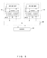
- Fig. 5 shows a configuration of a multi-CPU system to which the present invention is implemented.
- a CPUA 10, a CPUB 110, and memory 400 are connected to a SC 300.
- each of CPU core units 20 and 120 in the CPUA 10 and the CPUB 110, respectively, is connected to the SC 300 via external interface units 30 and 130, respectively.
- To each of the external interface units 30 and 130, either XCSC 40 or 140 and either XCRC 50 or 150 are provided respectively.
- the cross call between CPUs in Fig. 5 is, as an example, executed between the CPUA 10 and the CPUB 110 via the SC 300.
- FIG. 6 shows a configuration of the external interface unit of the CPUA 10 to which the present invention is implemented. It should be noted that although Fig. 6 shows the configuration of the external interface unit 30 of the CPUA 10 in Fig. 5 , the eternal interface unit 130 of the CPUB 110 has the same configuration.
- the CPU core unit 20 of the CPUA 10 is connected to the SC 300 via the external interface unit 30.
- the external interface unit 30 has an XCSC 40, an XCRC 50, and an arbitration unit 70.
- the XCSC 40 is for taking a control of cross call transmission
- the XCRC 50 is for taking a control of cross call reception.
- the arbitration unit 70 arbitrates the use right (priority) of a bus (a signal line) between the CPU core unit 20 and the SC 300, and takes a control so that the command issue is effectively performed in accordance with the specification.
- the XCSC 40 has a register 41, an ID identification circuit 42, an ID storage control circuit 43, an issue request switching circuit 44, an operation control unit 45, and a data register 60.
- the register 41 functions as a storage unit for collectively storing the BUSY state and NACK state of each cross call and command issue contents in order to manage the cross call.
- the ID identification circuit 42 identifies an identifier (ID) kept in a prescribed storage area of the register 41 based on the status information indicating the progress of the control operation by the XCSC 40.
- the ID storage control circuit 43 selects an identifier to be kept in the prescribed storage area of the register 41 in accordance with the status indicating the progress of the control operation by the XCSC 40.
- the issue request switching circuit 44 switches the cross call issue request and the transmission request of the data relating to the processing of the cross call in accordance with the status of use of the bus between the CPU core unit 20 and the SC 300.
- the operation control unit 45 is for performing the operation control of the XCSC 40.
- the data register 60 is for temporarily storing the cross call data transmitted from the CPU core unit 20.
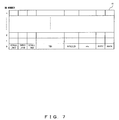
- Fig. 7 shows an example of the structure of the register 41 shown in Fig. 6 .
- the register 41 keeps and manages the processing status of the processing relating to the cross call i.e. the state of the cross call BUSY state (a cross call being issued) and the cross call NACK state (a cross call issue failed) with respect to each entry of the cross call, i.e. each of the pair numbers (BN number) of BUSY and NACK in this case.
- the register 41 keeps various data for managing the command issue status (indicated as "etc" in Fig. 7 ), and also keeps and manages a target ID (TID) that is an identifier indicating CPU etc. that is an ultimate destination of the cross call to be issued to the SC 1300 with respect to each BN number.
- the register 41 has a storage area referred to as HOLD_ID provided with respect to each BN number. In the storage area, any one of XCALL_REQ_ID, SWXC_REQ_ID and REQID is kept and managed.
- the XCALL_REQ_ID is an identifier individually assigned to each of issue requests in order to manage the issue requests of the XCALL_REQ (cross call request) that the XCSC 40 transmits to the arbitration unit 70.
- the SWXC_REQ_ID is an identifier individually assigned to each of issue requests in order to manage the issue requests of the SWXC_REQ (a transmission request of data relating to processing of a cross call) that the XCSC 40 transmits to the arbitration unit 70.
- REQID is an identifier for identifying individual cross calls.
- Fig. 8 shows a flow of transmission control operations of a cross call by the operation control unit 45 of the XCSC 40 in Fig. 6 , and additionally represents transition of each bit of the XCALL_VLD, XCALL_ISD, and SWXC_VLD that are status information indicating the progress of the control operations.
- S101 shows an initial state that is a state in which a cross call issued from the CPU core unit 20 and directed to another CPU connected to the SC 300 (CPUB 110 in a case of Fig. 5 ) can be received in the register 41.
- an issue request of XCALL_REQ (a cross call request) and a BN number corresponding to the XCALL_REQ are, first, transmitted from the CPU core unit 20.
- the control operation proceeds to S102 in which the XCSC 40 writes cross call data subsequently transmitted from the CPU core unit 20 in the data register 60 and sets the BUSY bit in the entry of the register 41 corresponding to the BN number transmitted with the issue request.
- the XCSC 40 transmits issue request of the XCALL_REQ to the arbitration unit 70, sets the XCALL_VLD bit corresponding to the BN number and indicates the completion of the issues request transmission.
- an XCALL_REQ_ID that is an identifier for identifying individual issue requests is generated and kept in the HOLD_ID in the corresponding entry in the register 41.
- the control operation proceeds to S103, and the XCSC 40 issues an XCALL_REQ to the SC 300, clears the XCALL_VLD bit in the entry the register 41, sets the XCALL_ISD bit in the entry instead, and indicates the completion of issues of the XCALL_REQ.
- the XCSC 40 generates REQID that is an identifier for identifying individual XCALL_REQ, and transmits the REQID with the XCALL_REQ to the SC 300. In the HOLD_ID of the entry of the register 41, the REQID is kept instead of the XCALL_REQ_ID.
- the control operation proceeds to S105, and the XCSC 40 transmits the issue request of the SWXC_REQ to the arbitration unit 70, clears the XCALL_ISD bit of the corresponding entry of the register 41, sets the SWXC_VLD bit of the corresponding entry instead, and indicates the completion of the issue request transmission.
- a SWXC_REQ_ID that is an identifier for identifying the individual issue requests is generated, and the SWXC_REQ_ID is kept instead of the REQID in the HOLD_ID of the corresponding entry of the register 41.
- the control operation proceeds to S106, and the XCSC 40 clears the SWXC_VLD bit of the corresponding entry of the register 41, transmits the SWXC_REQ including the data kept in the data register to the arbitration unit 70, and issues the data to the SC 300.
- the XCSC 40 clears the BUSY bit of the corresponding entry of the register 41, the control operation returns to S101, and the above-described control operations are conducted once again.
- each entry of the register 41 corresponding to the designated BN number at the time of an issue request of a cross call request from the CPU core unit 20 changes as described above in accordance with the flow of the control operations of cross call transmission in the XCSC 40. Therefore, the identifier currently kept in the HOLD_ID in the corresponding entry can be identified based on the status of the corresponding entry, i.e. state of each bit of XCALL_VALID, XCALL_ISD, and SWXC_VLD.
- Fig. 9 shows an example of the ID identification circuit 42.
- the ID identification circuit 42 determines what the identifier kept in the HOLD_ID of each entry of the register 41 indicates based on status information showing the progress of the above-described control operations by the XCSC 40.
- the ID identification circuit 42 is separately provided to each entry.
- match circuits 81a, 81b, and 81c generates "H” level output only when identifiers (ID) input in each of two inputs match one another.
- AND circuits 82a, 82b, and 82c generate "H” level output only when both of the two inputs are in "H” level.
- XCALL_ISD_ID_MCH that is an output of the AND circuit 82a is in "H” level when the identifier kept in the HOLD_ID of the entry to be determined of the register 41 is XCALL_REQ_ID.
- REQ_ISD_ID_MCH that is an output of the AND circuit 82b is in "H” level when the identifier kept in the HOLD_ID of the entry to be determined is REQ_ID.
- SWXC_ISD_ID_MCH is in "H” level when the identifier kept in the HOLD_ID of the entry to be determined is SWXC_REQ_ID.
- Fig. 9 as an input of the HOLD_ID, the identifier kept in the HOLD_ID of the entry corresponding to the designated BN number in the register 41 is input.
- XCALL_REQ_ID As an input of each of XCALL_REQ_ID, REQID, and SWXC_REQ_ID in Fig. 9 , an identifier with the same name generated in the manner described above in the XCSC 40 is input.
- XCALL_VLD, XCALL_ISD, and SWXC_VLD in Fig. 9 a state of each bit with the same name in the entry to be determined in the register 41 is input.
- Fig. 10 shows an example of a circuit of the ID storage control circuit 43.
- the ID storage control circuit 43 selects an ID to be kept in the HOLD_ID of the corresponding entry in accordance with the status of each entry of the register 41 using a part of the output from the ID identification circuit 42. Note that the ID storage control circuit 43 is also separately provided to each entry of the register 41.
- an AND circuit 91a generates an "H" level output only when both of the two inputs are in "H” level, i.e. the XCALL_ISD bit of the corresponding entry is set, and the XCALL_ISD_ID_MCH output from the ID identification circuit 42 is in "H” level.
- the output indicates that the XCSC 40 performed the control operations of S103 in Fig. 8 .
- the AND circuit 91b generates an "H" level output, only when both of the two inputs are in "H” level i.e. when ACK is returned from the SC 300 and XREQ_ISD_ID_MCH output from the ID identification circuit 42 is in "H” level.
- the output indicates that the XCSC 40 performed the control operations of S105 in Fig. 8 .
- the AND circuit 91c outputs REQID generated by the XCSC 40 performing the control operation of S103 shown in Fig. 8 when XCALL_ISD_ID_MCH output from the ID identification circuit 42 is in "H" level i.e. when the identifier kept in the HOLD_ID of the entry to be determined in the register 41 is XCALL_REQ_ID.
- the AND circuit 91d outputs SWXC_REQ_ID generated by the XCSC 40 performing the control operation of S105 shown in Fig. 8 when REQ_ISD_ID_MCH output from the ID identification circuit 42 is in "H" level i.e. when the identifier kept in the HOLD_ID of the entry to be determined in the register 41 is REQID.
- the OR circuit 92a generates an "H" level output when at least one or more of the three inputs that are XCALL_ISD bit of the corresponding entry, the AND circuits 91a and 91b are in "H” level.
- the XCALL_ISD bit of the corresponding entry is in "H” level when the XCSC 40 performs the control operation of S101 shown in Fig. 8 .
- the output of the OR circuit 92a is "H" level when the XCSC 40 performs any of the control operations of S101, S103, and S105 shown in Fig. 8 .
- the OR circuit 92b output any one of XCALL_REQ_ID, REQID, and SNXC_REQ_ID that are identifiers exclusively input to each of the three inputs.
- a storage area 93 represents an area of the HOLD_ID of the entry corresponding to the BN number designated in the register 41.
- EN indicated in Fig. 10
- the indication represents that the output of the OR circuit 92a operates as enable (ENABLE) of the data storage in the storage area 93.
- the storage area 93 operates so as to keep an identifier output from the OR circuit 92b.
- XCALL_REQ_ID is generated and the XCALL_VLD bit is set.
- the XCALL_REQ_ID is kept in the HOLD_ID (the storage area 63) in the entry of the register 41 corresponding to the BN number designated in the issue request of the cross call request transmitted from the CPU core unit 20.
- the ID storage control circuit 43 causes the HOLD_ID of each entry of the register 41 to keep the identifiers that need to be kept for internal processing of the XCSC 40 at every point of time in accordance with the flow of the transmission control operations of the XCSC 40.
- the storage area of the BN number provided in the command FIFO in the past is eliminated.
- the ID identification circuit 42 and the ID storage control circuit 43 the storage area for storing XCALL_REQ_ID, REQID, and SWXC_REQ_ID can be shared, and without increasing the storage area compared with the conventional art, control of increase in the hardware resources in the cross call control can be achieved.
- the effect of control of increase in the hardware resources by control change of the entries of the register can be roughly estimated from (effect of increase control per entry)x(number of entries)x(strand count).
- the strand count is the number of logical cores established per physical CPU core. Because both of the number of entries and the strand count are tend to increase due to the advancement of the multi-core of the CPUs and introduction of the multi-thread processing in the recent years, the effect of increase control should be a profound effect.
- Fig. 11 shows an example of a circuit of the issue request switching circuit 44.
- the XCSC 40 is controlled as below.
- the control is such that the SWXC_REQ issue request is suppressed; however, the XCALL_REQ issue request is transmitted from the XCSC 40 to the arbitration unit 70 in such a period of time.
- the BUSY flag is off, i.e.
- the control is such that the SWXC_REQ issue request is preferentially transmitted to the arbitration unit 70, and when there is no SWXC_REQ issue request, the XCALL_REQ issue request is transmitted to the arbitration unit 70.
- the issue request of XCALL_REQ and the issue request of SWXC_REQ corresponding to the identical BN number are not generated at the same time but are exclusively generated, and for that reason, the cross call operations are not disrupted by such a control.
- the issues request switching circuit 44 is a circuit for performing such a control.
- an OR circuit 101 generates an "H" level output when at least one or more of the two inputs is in “H” level, i.e. when at least one or more of each of the outputs of two AND circuits 102a and 102b is in "H" level.
- the output of the AND circuit 102a becomes "H” level only when an XCALL_REQ_PRE bit is in "H” level under a situation in which the BUSY bit (DATA_BUSY) indicating the status of use of the bus between the CPU core unit 20 and the SC 300 is set.
- the XCALL_REQ_PRE bit is a bit set (to be in "H” level) in the XCSC 40 as a trigger for generating the XCALL_REQ issue request when the transmission control operation of the XCSC 40 shown in Fig. 8 proceeds to S102.
- the AND circuit 102a becomes "H" level.
- the output of the AND circuit 102b becomes "H” level only when in the state in which the corresponding BUSY bit is not set and when the XCALL_ERQ_PRE bit becomes "H” level under the condition that the SWXC_REQ_PRE bit is "L” level.
- the SWXC_REQ_PRE is a bit set (to be in "H” level) in the XCSC 40 as a trigger for generating the SWXC_REQ issue request when the transmission control operation of the XCSC 40 shown in Fig. 8 proceeds to S105.
- An OR circuit 71 recognizes the XCALL_REQ as "H" level and permits the transmission of the XCALL_REQ issue request to the arbitration unit 70.
- the AND circuit 102a only when the SWXC_REQ_PRE becomes "H” level under the condition such that the corresponding BUSY bit is not set, i.e. when the SWXC_REQ issue request is generated in a period of time in which the data transmission via the bus is not performed, recognizes the SWXC_REQ as "H” level, and permits the transmission of the SWXC_REQ issue request to the arbitration unit 70.
- the wiring for the XCALL_REQ can be shared with the wiring for the SWXC_REQ from the XCSC 40 to the arbitration unit 70, and consequently, an amount of wiring around the arbitration unit 70 where the wiring is gathered for the arbitration with other requests from the CPU core unit 20 is decreased compared with a case in which the signal lines are individually connected to the arbitration unit 70.
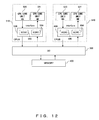
- FIG. 12 The configuration of the multi-CPU system is shown in Fig. 12 .
- a CPUA 510, a CPUB 610, and memory 400 are connected to a SC 300.
- the CPUA 510 has a CPU core unit AA520 and a CPU core unit AB521
- the CPUB 610 has a CPU core unit BA620 and a CPU core unit BB 621.
- Both of the CPU core unit AA 520 and the CPU core unit AB 521 are connected to the SC 300 via an external interface unit 530
- both of the CPU core unit BA620 and the CPU core unit BB621 are connected to the SC 300 via an external interface unit 630.
- XCSCs 540 and 640, respectively, and XCRCs 550 and 650, respectively are provided in the external interface units 530 and 630.
- Fig. 13 shows the configuration of the external interface unit 530 of the CPUA 510 shown in Fig. 12 .
- the external interface unit 630 of the CPUB 610 shown in Fig. 12 has the same configuration.
- Both of the CPU core unit AA520 and the CPU core unit AB521 of the CPUA 510 are connected to the SC 300 via the external interface unit 530.
- the control of the cross call is performed by the external interface unit 530.
- the external interface unit 530 has an XCSC 540, an XCRC 550, and an arbitration unit 570.
- the XCSC 540 performs transmission control of the cross call
- the XCRC 550 performs reception control of the cross call.
- the arbitration unit 570 arbitrates the use right (priority order) of a bus (signal line) between two CPU core units 520 and 521 and the SC 300, and takes a control so that the command issue can be efficiently performed in accordance with the specification.
- the configuration of the XCSC 540 has a register 542, an ID identification circuit 542, an ID storage control circuit 543, an issue request switching circuit 544, an operation control circuit 545, and a data register 560.
- the register 541 functions as a storage unit for collectively storing the state of BUSY and NACK of each cross call and the contents of the issued command for management of the cross calls.
- the register 541 has a register 541-1 for the CPU core unit AA520 and a register 541-2 for the CPU core unit AB521.
- the configurations of the registers 541-1 and 541-2 are the same as the configuration of the register 41 shown in Fig. 7 .
- the ID identification circuit 542 identifies an identifier (ID) kept in a prescribed storage area of the register 541 based on the status information that indicates the progress of the control operation by the XCSC 540, and has a configuration identical to that of the ID identification circuit 42 shown in Fig. 9 .
- the ID storage control circuit 543 selects an identifier to be kept in the prescribed storage area of the register 541 in accordance with the status that indicates the progress of the control operations by the XCSC 540, and has a configuration identical to that of the ID storage control circuit 43 shown in Fig. 10 .
- the issue request switching circuit 544 switches the cross call issue request and the transmission request of the data relating to the processing of the cross call in accordance with the status of use of the bus between the two CPU core units 520, 521 and the SC 300, and has a configuration identical to that of the issue request switching circuit 44 shown in Fig. 11 .
- the operation control unit 545 is for performing the operation control of the XCSC 540, and the flow of the transmission control operations of a cross call of the XCSC 40 performed by the operation control unit 545 is identical to the flow shown in Fig. 8 .
- the data register 460 is for temporarily storing the cross call data transmitted from the two CPU core units 520 and 521.
- the storage area of the BN number provided in the command FIFO is eliminated in the past.
- the ID identification circuit 542 and the ID storage control circuit 543 as described above, the storage area for storing XCALL_REQ_ID, REQID, and SWXC_REQ_ID in the registers 541-1 and 541-2 can be shared, and as a result, without increasing the storage area compared with the conventional art, it is possible to handle the change in the specification in the cross call control.
- the effect of control of increase in the hardware resources by control change of the entries of the register can be roughly estimated from (effect of increase control per entry) ⁇ (number of entries) ⁇ (strand count) ⁇ (number of CPU cores). Accordingly, like the CPU having a single CPU core described above, in the CPU having plural CPU cores, the effect of hardware increase control should be a profound effect.
Landscapes
- Engineering & Computer Science (AREA)
- Theoretical Computer Science (AREA)
- Software Systems (AREA)
- Physics & Mathematics (AREA)
- General Engineering & Computer Science (AREA)
- General Physics & Mathematics (AREA)
- Computer Hardware Design (AREA)
- Multi Processors (AREA)
Applications Claiming Priority (2)
| Application Number | Priority Date | Filing Date | Title |
|---|---|---|---|
| JP2005290888A JP4856413B2 (ja) | 2005-10-04 | 2005-10-04 | 演算処理装置、情報処理装置、及び演算処理装置の制御方法 |
| PCT/JP2005/023251 WO2007039933A1 (fr) | 2005-10-04 | 2005-12-19 | Dispositif de traitement de fonctionnement |
Publications (3)
| Publication Number | Publication Date |
|---|---|
| EP1936514A1 true EP1936514A1 (fr) | 2008-06-25 |
| EP1936514A4 EP1936514A4 (fr) | 2010-04-21 |
| EP1936514B1 EP1936514B1 (fr) | 2012-12-19 |
Family
ID=37905979
Family Applications (1)
| Application Number | Title | Priority Date | Filing Date |
|---|---|---|---|
| EP05816411A Expired - Lifetime EP1936514B1 (fr) | 2005-10-04 | 2005-12-19 | Appareil et méthode de contrôle d'envoi de requêtes vers un dispositif de traitement d'operations |
Country Status (6)
| Country | Link |
|---|---|
| US (1) | US20080189719A1 (fr) |
| EP (1) | EP1936514B1 (fr) |
| JP (1) | JP4856413B2 (fr) |
| KR (1) | KR100990399B1 (fr) |
| CN (1) | CN101278277B (fr) |
| WO (1) | WO2007039933A1 (fr) |
Cited By (1)
| Publication number | Priority date | Publication date | Assignee | Title |
|---|---|---|---|---|
| EP2704009A3 (fr) * | 2012-08-31 | 2015-01-14 | Fujitsu Limited | Appareil de traitement d' informations, procédé et programme de traitement d'informations |
Families Citing this family (3)
| Publication number | Priority date | Publication date | Assignee | Title |
|---|---|---|---|---|
| KR20100003784A (ko) | 2008-07-02 | 2010-01-12 | 주식회사 만도 | 브레이크시스템용 솔레노이드밸브 및 그 제조방법 |
| US8918509B1 (en) * | 2011-12-20 | 2014-12-23 | The Mathworks, Inc. | Dynamic arbitrary data simulation using fixed resources |
| US9256502B2 (en) * | 2012-06-19 | 2016-02-09 | Oracle International Corporation | Method and system for inter-processor communication |
Family Cites Families (8)
| Publication number | Priority date | Publication date | Assignee | Title |
|---|---|---|---|---|
| US5555420A (en) * | 1990-12-21 | 1996-09-10 | Intel Corporation | Multiprocessor programmable interrupt controller system with separate interrupt bus and bus retry management |
| US5689713A (en) * | 1995-03-31 | 1997-11-18 | Sun Microsystems, Inc. | Method and apparatus for interrupt communication in a packet-switched computer system |
| US5907485A (en) * | 1995-03-31 | 1999-05-25 | Sun Microsystems, Inc. | Method and apparatus for flow control in packet-switched computer system |
| US5893165A (en) * | 1996-07-01 | 1999-04-06 | Sun Microsystems, Inc. | System and method for parallel execution of memory transactions using multiple memory models, including SSO, TSO, PSO and RMO |
| US6154816A (en) * | 1997-10-24 | 2000-11-28 | Compaq Computer Corp. | Low occupancy protocol for managing concurrent transactions with dependencies |
| JP2003242097A (ja) * | 2002-02-15 | 2003-08-29 | Hitachi Ltd | クロスコール機能を備えるディスク制御装置 |
| US6922804B2 (en) * | 2002-03-08 | 2005-07-26 | Hewlett-Packard Development Company, L.P. | Dynamic end to end retransmit apparatus and method |
| US7188229B2 (en) * | 2004-01-17 | 2007-03-06 | Sun Microsystems, Inc. | Method and apparatus for memory management in a multi-processor computer system |
-
2005
- 2005-10-04 JP JP2005290888A patent/JP4856413B2/ja not_active Expired - Fee Related
- 2005-12-19 CN CN2005800517695A patent/CN101278277B/zh not_active Expired - Fee Related
- 2005-12-19 WO PCT/JP2005/023251 patent/WO2007039933A1/fr not_active Ceased
- 2005-12-19 EP EP05816411A patent/EP1936514B1/fr not_active Expired - Lifetime
- 2005-12-19 KR KR1020087009682A patent/KR100990399B1/ko not_active Expired - Fee Related
-
2008
- 2008-04-03 US US12/062,185 patent/US20080189719A1/en not_active Abandoned
Cited By (2)
| Publication number | Priority date | Publication date | Assignee | Title |
|---|---|---|---|---|
| EP2704009A3 (fr) * | 2012-08-31 | 2015-01-14 | Fujitsu Limited | Appareil de traitement d' informations, procédé et programme de traitement d'informations |
| US9063929B2 (en) | 2012-08-31 | 2015-06-23 | Fujitsu Limited | Information processing apparatus, information processing method, computer-readable recording medium having stored therein program |
Also Published As
| Publication number | Publication date |
|---|---|
| CN101278277A (zh) | 2008-10-01 |
| KR20080063777A (ko) | 2008-07-07 |
| KR100990399B1 (ko) | 2010-10-29 |
| EP1936514A4 (fr) | 2010-04-21 |
| WO2007039933A1 (fr) | 2007-04-12 |
| EP1936514B1 (fr) | 2012-12-19 |
| CN101278277B (zh) | 2011-06-08 |
| JP4856413B2 (ja) | 2012-01-18 |
| US20080189719A1 (en) | 2008-08-07 |
| JP2007102447A (ja) | 2007-04-19 |
Similar Documents
| Publication | Publication Date | Title |
|---|---|---|
| US7533197B2 (en) | System and method for remote direct memory access without page locking by the operating system | |
| KR100268565B1 (ko) | 다중 처리 시스템에서 타스크를 큐잉하기 위한 시스템 및 방법 | |
| US20080109569A1 (en) | Remote DMA systems and methods for supporting synchronization of distributed processes in a multi-processor system using collective operations | |
| EP2187316B1 (fr) | Système de stockage commandé par porte et contrôleur de synchronisation et procédé pour processeurs multiprocessus | |
| US20080109573A1 (en) | RDMA systems and methods for sending commands from a source node to a target node for local execution of commands at the target node | |
| US20090271796A1 (en) | Information processing system and task execution control method | |
| US5625846A (en) | Transfer request queue control system using flags to indicate transfer request queue validity and whether to use round-robin system for dequeuing the corresponding queues | |
| EP0599449A2 (fr) | Système et méthode de communication de données | |
| US7234004B2 (en) | Method, apparatus and program product for low latency I/O adapter queuing in a computer system | |
| KR20130111167A (ko) | 정보 처리 장치, 연산 장치 및 정보 전송 방법 | |
| US7640549B2 (en) | System and method for efficiently exchanging data among processes | |
| JP2012073851A (ja) | バスシステムおよびそのデッドロック回避回路 | |
| US8086766B2 (en) | Support for non-locking parallel reception of packets belonging to a single memory reception FIFO | |
| JP5360061B2 (ja) | マルチプロセッサシステム及びその制御方法 | |
| US20080189719A1 (en) | Operation processor apparatus | |
| US10318424B2 (en) | Information processing device | |
| US20080109604A1 (en) | Systems and methods for remote direct memory access to processor caches for RDMA reads and writes | |
| JP2002530736A5 (fr) | ||
| US8762603B2 (en) | Addressable FIFO | |
| US20090210653A1 (en) | Method and device for treating and processing data | |
| CN112506676A (zh) | 进程间的数据传输方法、计算机设备和存储介质 | |
| CN119441114A (zh) | 一种信息同步方法及装置 | |
| US7916146B1 (en) | Halt context switching method and system | |
| EP1249757B1 (fr) | Réglage d'interruptions pour communication entre processus | |
| JPH11212900A (ja) | システム制御装置 |
Legal Events
| Date | Code | Title | Description |
|---|---|---|---|
| PUAI | Public reference made under article 153(3) epc to a published international application that has entered the european phase |
Free format text: ORIGINAL CODE: 0009012 |
|
| 17P | Request for examination filed |
Effective date: 20080331 |
|
| AK | Designated contracting states |
Kind code of ref document: A1 Designated state(s): DE FR GB |
|
| DAX | Request for extension of the european patent (deleted) | ||
| RBV | Designated contracting states (corrected) |
Designated state(s): DE FR GB |
|
| A4 | Supplementary search report drawn up and despatched |
Effective date: 20100322 |
|
| RIC1 | Information provided on ipc code assigned before grant |
Ipc: G06F 15/167 20060101ALI20100316BHEP Ipc: G06F 13/24 20060101ALI20100316BHEP Ipc: G06F 13/36 20060101ALI20100316BHEP Ipc: G06F 15/17 20060101AFI20070605BHEP |
|
| RIC1 | Information provided on ipc code assigned before grant |
Ipc: G06F 9/48 20060101ALI20120213BHEP Ipc: G06F 9/50 20060101ALI20120213BHEP Ipc: G06F 13/24 20060101ALI20120213BHEP Ipc: G06F 15/167 20060101ALI20120213BHEP Ipc: G06F 13/36 20060101ALI20120213BHEP Ipc: G06F 15/17 20060101AFI20120213BHEP |
|
| RTI1 | Title (correction) |
Free format text: APPARATUS AND METHOD FOR CONTROLLING ISSUE OF REQUESTS TO ANOTHER OPERATION PROCESSING DEVICE |
|
| GRAP | Despatch of communication of intention to grant a patent |
Free format text: ORIGINAL CODE: EPIDOSNIGR1 |
|
| GRAS | Grant fee paid |
Free format text: ORIGINAL CODE: EPIDOSNIGR3 |
|
| GRAA | (expected) grant |
Free format text: ORIGINAL CODE: 0009210 |
|
| AK | Designated contracting states |
Kind code of ref document: B1 Designated state(s): DE FR GB |
|
| REG | Reference to a national code |
Ref country code: GB Ref legal event code: FG4D |
|
| REG | Reference to a national code |
Ref country code: DE Ref legal event code: R096 Ref document number: 602005037529 Country of ref document: DE Effective date: 20130207 |
|
| PLBE | No opposition filed within time limit |
Free format text: ORIGINAL CODE: 0009261 |
|
| STAA | Information on the status of an ep patent application or granted ep patent |
Free format text: STATUS: NO OPPOSITION FILED WITHIN TIME LIMIT |
|
| 26N | No opposition filed |
Effective date: 20130920 |
|
| REG | Reference to a national code |
Ref country code: DE Ref legal event code: R097 Ref document number: 602005037529 Country of ref document: DE Effective date: 20130920 |
|
| PGFP | Annual fee paid to national office [announced via postgrant information from national office to epo] |
Ref country code: DE Payment date: 20140131 Year of fee payment: 9 |
|
| PGFP | Annual fee paid to national office [announced via postgrant information from national office to epo] |
Ref country code: FR Payment date: 20140131 Year of fee payment: 9 |
|
| PGFP | Annual fee paid to national office [announced via postgrant information from national office to epo] |
Ref country code: GB Payment date: 20140206 Year of fee payment: 9 |
|
| REG | Reference to a national code |
Ref country code: DE Ref legal event code: R119 Ref document number: 602005037529 Country of ref document: DE |
|
| GBPC | Gb: european patent ceased through non-payment of renewal fee |
Effective date: 20141219 |
|
| REG | Reference to a national code |
Ref country code: FR Ref legal event code: ST Effective date: 20150831 |
|
| PG25 | Lapsed in a contracting state [announced via postgrant information from national office to epo] |
Ref country code: GB Free format text: LAPSE BECAUSE OF NON-PAYMENT OF DUE FEES Effective date: 20141219 Ref country code: DE Free format text: LAPSE BECAUSE OF NON-PAYMENT OF DUE FEES Effective date: 20150701 |
|
| PG25 | Lapsed in a contracting state [announced via postgrant information from national office to epo] |
Ref country code: FR Free format text: LAPSE BECAUSE OF NON-PAYMENT OF DUE FEES Effective date: 20141231 |