EP2051047A1 - Reflective encoder, scale thereof, and method for manufacturing scale - Google Patents
Reflective encoder, scale thereof, and method for manufacturing scale Download PDFInfo
- Publication number
- EP2051047A1 EP2051047A1 EP07744609A EP07744609A EP2051047A1 EP 2051047 A1 EP2051047 A1 EP 2051047A1 EP 07744609 A EP07744609 A EP 07744609A EP 07744609 A EP07744609 A EP 07744609A EP 2051047 A1 EP2051047 A1 EP 2051047A1
- Authority
- EP
- European Patent Office
- Prior art keywords
- dielectric substance
- light
- scale
- pattern
- patterns
- Prior art date
- Legal status (The legal status is an assumption and is not a legal conclusion. Google has not performed a legal analysis and makes no representation as to the accuracy of the status listed.)
- Granted
Links
- 238000004519 manufacturing process Methods 0.000 title claims description 8
- 238000000034 method Methods 0.000 title description 14
- 239000000126 substance Substances 0.000 claims abstract description 73
- 230000003287 optical effect Effects 0.000 claims description 33
- 239000000758 substrate Substances 0.000 claims description 14
- VYPSYNLAJGMNEJ-UHFFFAOYSA-N Silicium dioxide Chemical group O=[Si]=O VYPSYNLAJGMNEJ-UHFFFAOYSA-N 0.000 claims description 8
- 238000000059 patterning Methods 0.000 claims description 8
- 229910052814 silicon oxide Inorganic materials 0.000 claims description 8
- 238000005259 measurement Methods 0.000 claims description 7
- 238000005530 etching Methods 0.000 claims description 6
- 239000010410 layer Substances 0.000 description 56
- 238000001514 detection method Methods 0.000 description 13
- 238000005516 engineering process Methods 0.000 description 5
- 239000011521 glass Substances 0.000 description 5
- 230000014509 gene expression Effects 0.000 description 4
- NRTOMJZYCJJWKI-UHFFFAOYSA-N Titanium nitride Chemical compound [Ti]#N NRTOMJZYCJJWKI-UHFFFAOYSA-N 0.000 description 2
- QDOXWKRWXJOMAK-UHFFFAOYSA-N dichromium trioxide Chemical compound O=[Cr]O[Cr]=O QDOXWKRWXJOMAK-UHFFFAOYSA-N 0.000 description 2
- 229910010272 inorganic material Inorganic materials 0.000 description 2
- 239000011147 inorganic material Substances 0.000 description 2
- 238000001459 lithography Methods 0.000 description 2
- VYZAMTAEIAYCRO-UHFFFAOYSA-N Chromium Chemical compound [Cr] VYZAMTAEIAYCRO-UHFFFAOYSA-N 0.000 description 1
- 230000005856 abnormality Effects 0.000 description 1
- 230000015572 biosynthetic process Effects 0.000 description 1
- 230000003247 decreasing effect Effects 0.000 description 1
- 238000006073 displacement reaction Methods 0.000 description 1
- 239000000463 material Substances 0.000 description 1
- 229910052751 metal Inorganic materials 0.000 description 1
- 239000002184 metal Substances 0.000 description 1
- 238000007790 scraping Methods 0.000 description 1
- 238000000926 separation method Methods 0.000 description 1
- 239000002344 surface layer Substances 0.000 description 1
- 230000002194 synthesizing effect Effects 0.000 description 1
Images






Classifications
-
- G—PHYSICS
- G01—MEASURING; TESTING
- G01D—MEASURING NOT SPECIALLY ADAPTED FOR A SPECIFIC VARIABLE; ARRANGEMENTS FOR MEASURING TWO OR MORE VARIABLES NOT COVERED IN A SINGLE OTHER SUBCLASS; TARIFF METERING APPARATUS; MEASURING OR TESTING NOT OTHERWISE PROVIDED FOR
- G01D5/00—Mechanical means for transferring the output of a sensing member; Means for converting the output of a sensing member to another variable where the form or nature of the sensing member does not constrain the means for converting; Transducers not specially adapted for a specific variable
- G01D5/26—Mechanical means for transferring the output of a sensing member; Means for converting the output of a sensing member to another variable where the form or nature of the sensing member does not constrain the means for converting; Transducers not specially adapted for a specific variable characterised by optical transfer means, i.e. using infrared, visible, or ultraviolet light
- G01D5/32—Mechanical means for transferring the output of a sensing member; Means for converting the output of a sensing member to another variable where the form or nature of the sensing member does not constrain the means for converting; Transducers not specially adapted for a specific variable characterised by optical transfer means, i.e. using infrared, visible, or ultraviolet light with attenuation or whole or partial obturation of beams of light
- G01D5/34—Mechanical means for transferring the output of a sensing member; Means for converting the output of a sensing member to another variable where the form or nature of the sensing member does not constrain the means for converting; Transducers not specially adapted for a specific variable characterised by optical transfer means, i.e. using infrared, visible, or ultraviolet light with attenuation or whole or partial obturation of beams of light the beams of light being detected by photocells
- G01D5/347—Mechanical means for transferring the output of a sensing member; Means for converting the output of a sensing member to another variable where the form or nature of the sensing member does not constrain the means for converting; Transducers not specially adapted for a specific variable characterised by optical transfer means, i.e. using infrared, visible, or ultraviolet light with attenuation or whole or partial obturation of beams of light the beams of light being detected by photocells using displacement encoding scales
- G01D5/34746—Linear encoders
-
- G—PHYSICS
- G01—MEASURING; TESTING
- G01D—MEASURING NOT SPECIALLY ADAPTED FOR A SPECIFIC VARIABLE; ARRANGEMENTS FOR MEASURING TWO OR MORE VARIABLES NOT COVERED IN A SINGLE OTHER SUBCLASS; TARIFF METERING APPARATUS; MEASURING OR TESTING NOT OTHERWISE PROVIDED FOR
- G01D5/00—Mechanical means for transferring the output of a sensing member; Means for converting the output of a sensing member to another variable where the form or nature of the sensing member does not constrain the means for converting; Transducers not specially adapted for a specific variable
- G01D5/26—Mechanical means for transferring the output of a sensing member; Means for converting the output of a sensing member to another variable where the form or nature of the sensing member does not constrain the means for converting; Transducers not specially adapted for a specific variable characterised by optical transfer means, i.e. using infrared, visible, or ultraviolet light
- G01D5/32—Mechanical means for transferring the output of a sensing member; Means for converting the output of a sensing member to another variable where the form or nature of the sensing member does not constrain the means for converting; Transducers not specially adapted for a specific variable characterised by optical transfer means, i.e. using infrared, visible, or ultraviolet light with attenuation or whole or partial obturation of beams of light
- G01D5/34—Mechanical means for transferring the output of a sensing member; Means for converting the output of a sensing member to another variable where the form or nature of the sensing member does not constrain the means for converting; Transducers not specially adapted for a specific variable characterised by optical transfer means, i.e. using infrared, visible, or ultraviolet light with attenuation or whole or partial obturation of beams of light the beams of light being detected by photocells
- G01D5/347—Mechanical means for transferring the output of a sensing member; Means for converting the output of a sensing member to another variable where the form or nature of the sensing member does not constrain the means for converting; Transducers not specially adapted for a specific variable characterised by optical transfer means, i.e. using infrared, visible, or ultraviolet light with attenuation or whole or partial obturation of beams of light the beams of light being detected by photocells using displacement encoding scales
-
- G—PHYSICS
- G01—MEASURING; TESTING
- G01D—MEASURING NOT SPECIALLY ADAPTED FOR A SPECIFIC VARIABLE; ARRANGEMENTS FOR MEASURING TWO OR MORE VARIABLES NOT COVERED IN A SINGLE OTHER SUBCLASS; TARIFF METERING APPARATUS; MEASURING OR TESTING NOT OTHERWISE PROVIDED FOR
- G01D5/00—Mechanical means for transferring the output of a sensing member; Means for converting the output of a sensing member to another variable where the form or nature of the sensing member does not constrain the means for converting; Transducers not specially adapted for a specific variable
- G01D5/26—Mechanical means for transferring the output of a sensing member; Means for converting the output of a sensing member to another variable where the form or nature of the sensing member does not constrain the means for converting; Transducers not specially adapted for a specific variable characterised by optical transfer means, i.e. using infrared, visible, or ultraviolet light
- G01D5/32—Mechanical means for transferring the output of a sensing member; Means for converting the output of a sensing member to another variable where the form or nature of the sensing member does not constrain the means for converting; Transducers not specially adapted for a specific variable characterised by optical transfer means, i.e. using infrared, visible, or ultraviolet light with attenuation or whole or partial obturation of beams of light
- G01D5/34—Mechanical means for transferring the output of a sensing member; Means for converting the output of a sensing member to another variable where the form or nature of the sensing member does not constrain the means for converting; Transducers not specially adapted for a specific variable characterised by optical transfer means, i.e. using infrared, visible, or ultraviolet light with attenuation or whole or partial obturation of beams of light the beams of light being detected by photocells
- G01D5/347—Mechanical means for transferring the output of a sensing member; Means for converting the output of a sensing member to another variable where the form or nature of the sensing member does not constrain the means for converting; Transducers not specially adapted for a specific variable characterised by optical transfer means, i.e. using infrared, visible, or ultraviolet light with attenuation or whole or partial obturation of beams of light the beams of light being detected by photocells using displacement encoding scales
- G01D5/34707—Scales; Discs, e.g. fixation, fabrication, compensation
-
- G—PHYSICS
- G01—MEASURING; TESTING
- G01D—MEASURING NOT SPECIALLY ADAPTED FOR A SPECIFIC VARIABLE; ARRANGEMENTS FOR MEASURING TWO OR MORE VARIABLES NOT COVERED IN A SINGLE OTHER SUBCLASS; TARIFF METERING APPARATUS; MEASURING OR TESTING NOT OTHERWISE PROVIDED FOR
- G01D5/00—Mechanical means for transferring the output of a sensing member; Means for converting the output of a sensing member to another variable where the form or nature of the sensing member does not constrain the means for converting; Transducers not specially adapted for a specific variable
- G01D5/26—Mechanical means for transferring the output of a sensing member; Means for converting the output of a sensing member to another variable where the form or nature of the sensing member does not constrain the means for converting; Transducers not specially adapted for a specific variable characterised by optical transfer means, i.e. using infrared, visible, or ultraviolet light
- G01D5/32—Mechanical means for transferring the output of a sensing member; Means for converting the output of a sensing member to another variable where the form or nature of the sensing member does not constrain the means for converting; Transducers not specially adapted for a specific variable characterised by optical transfer means, i.e. using infrared, visible, or ultraviolet light with attenuation or whole or partial obturation of beams of light
- G01D5/34—Mechanical means for transferring the output of a sensing member; Means for converting the output of a sensing member to another variable where the form or nature of the sensing member does not constrain the means for converting; Transducers not specially adapted for a specific variable characterised by optical transfer means, i.e. using infrared, visible, or ultraviolet light with attenuation or whole or partial obturation of beams of light the beams of light being detected by photocells
- G01D5/347—Mechanical means for transferring the output of a sensing member; Means for converting the output of a sensing member to another variable where the form or nature of the sensing member does not constrain the means for converting; Transducers not specially adapted for a specific variable characterised by optical transfer means, i.e. using infrared, visible, or ultraviolet light with attenuation or whole or partial obturation of beams of light the beams of light being detected by photocells using displacement encoding scales
- G01D5/34776—Absolute encoders with analogue or digital scales
- G01D5/34792—Absolute encoders with analogue or digital scales with only digital scales or both digital and incremental scales
Definitions
- the present invention relates to a reflection type encoder, a scale thereof and a method for producing the scale, and in particular to a reflection type encoder, a scale thereof and a method for producing the scale, which are preferably used for a photoelectric type encoder such as a linear encoder and a rotary encoder, etc., and capable of achieving an incremental (INC) pattern and an origin (ABS) pattern in a single track.
- a photoelectric type encoder such as a linear encoder and a rotary encoder, etc.
- Metal such as chrome, etc., or a dielectric substance such as silicon oxide, etc., are formed, as a film, on the scale used in a photoelectric type encoder such as a linear encoder and a rotary encoder, and patterns are formed thereon.
- an origin pattern is provided in addition to an INC pattern, and for example, the origin pattern is forcedly passed through immediately after the power is turned on, and correction of a detection position is carried out.
- Fig. 2 corresponding to Fig.1 of Japanese Translation of International Application (Kohyo) No. 2004-529344 (Patent Document 2)
- Patent Document 2 such a technology has been proposed, in which an INC pattern 10 shown in Stage A and having repeated patterns of reflection lines 12 and non-reflection lines 14 and an ABS pattern 16 shown in Stage B and having reflection lines 12 and non-reflection lines 14 are combined to make a scale 18, and as shown in Stages C and D, a part (22) of reflection lines 20 of the INC pattern 10 are fractured, and the fractured portion 22 is made into the ABS data.
- reference numeral 20 denotes a reflection line as it is in an original state
- 22 denotes a cut-off reflection line.
- a detector 50 of the INC pattern and a detector 26 of the ABS pattern are disposed in the axial direction of measurement apart from each other.
- reference symbols LS1 and LS2 denote light sources.
- Reference numeral 18 denotes a scale
- 25 denotes an image-forming lens
- 52 denotes an index grating
- 54 denotes a reading head.
- reference numerals 4 1 , 6 1 , 7 1 and 9 1 denote metallic layers
- reference numeral 5 1 denotes a non-absorbing interference layer of an inorganic material corresponding to the first color tone
- reference numeral 8 1 denotes a non-absorbing interference layer of an inorganic material corresponding to the second color tone.
- Patent Document 3 has a multi-color minute structure with the pattern heights changed in a minute map, the technology does not pertain to the scale of a photoelectric encoder.
- the present invention was developed to solve the problems in the prior arts, which are described above, and it is therefore an object of the present invention to downsize the scale of a reflection type encoder by overlapping a plurality of patterns on the same axis.
- a first aspect of the invention of the present application is a reflection type encoder, which receives a plurality of light-receiving signals from a single scale, including a light source, a scale having a plurality of patterns formed thereon to which light is irradiated from the light source, and a light-receiving element for receiving light reflected from each of the plurality of patterns, wherein a plurality of patterns each having different thicknesses are formed on a single track of the scale by using a dielectric substance, light of a plurality of wavelengths each having different brightnesses in accordance with differences in the thickness of the dielectric substance is irradiated from the light source, and a light-receiving signal is obtained for the respective thicknesses of the dielectric substance.
- a second aspect of the invention of the present application is that the encoder detects a first pattern at a first optical wavelength at which reflection light attenuates by a dielectric substance layer of a first thickness, and detects a second pattern at a second optical wavelength at which reflection light attenuates by a dielectric substance layer of a second thickness.
- a third aspect of the invention of the present application is that a height of the dielectric substance layer is set so that the light quantity from the dielectric substance layer is minimized at the first optical wavelength and the light quantity from the dielectric substance layer is maximized at the second optical wavelength.
- a fourth aspect of the invention of the present application is that the plurality of patterns are an INC pattern and an ABS pattern.
- a fifth aspect of the invention of the present application is that the dielectric substance is silicon oxide.
- a sixth aspect of the invention of the present application is that the thicknesses of the dielectric substance are 430nm and 330nm, and the wavelengths of the light source are 880nm and 660nm.
- a seventh aspect of the invention of the present application is that the detection center axis of the light-receiving element for detecting the incremental pattern is in agreement with the detection center axis of the light-receiving element for detecting the ABS pattern on the measurement axis.
- an eighth aspect of the invention of the present application provides a scale of a reflection type encoder characterized in that a plurality of patterns each having different thicknesses are formed on a single track of the scale by using a dielectric substance.
- a ninth aspect of the invention of the present application provides a method for producing a scale, including the steps of, when forming a plurality of patterns each having different thicknesses on a single track of the scale by using a dielectric substance: forming a light reflection layer on a scale substrate; forming a dielectric substance layer with a first height thereon; forming and patterning a first resist pattern thereon; etching the dielectric substance layer of the first resist pattern opening portion up to a second height; forming and patterning a second resist pattern thereon; etching the dielectric substance layer of the second resist pattern opening portion; and removing the second resist pattern.
- a tenth aspect of the invention of the present application provides a method for producing a scale, including the steps of, when forming a plurality of patterns each having different thicknesses on a single track of the scale by using a dielectric substance: forming a light reflection layer on a scale substrate; forming and patterning a first resist pattern thereon; lifting off a dielectric substance layer of a second height at the first resist pattern opening portion; removing the first resist pattern; forming and patterning a second resist pattern thereon; lifting off a dielectric substance layer of a first height at the second resist pattern opening portion; and removing the second resist pattern.
- the INC pattern and ABS pattern are overlapped on the same single track, wherein the scale can be downsized.
- the detection accuracy of the respective patterns can be improved since the respective patterns are not influenced by each other in respective pattern detection.
- a scale used in the present embodiment separates an INC pattern and an ABS pattern from each other by controlling the thickness (heights) h 1 and h 2 of a dielectric substance layer 34 formed on a light reflection layer 32 formed on a scale substrate 30.
- a pattern in which the thickness of the dielectric substance layer is h 1 can be made into an INC pattern 36
- a pattern in which the thickness of the dielectric substance layer is h 2 can be made into an ABS pattern 38.
- silicon oxide (SiO 2 ), chrome oxide (Cr 2 O 3 ), titanium nitride (TiN), etc. may be used as a material of the dielectric substance layer 34. Since a difference in thickness of the dielectric substance layer can be increased if silicon oxide is used, light separation can be facilitated, and a high-performance encoder can be attained. On the other hand, since the refractive index n of chrome oxide or titanium nitride is larger than that of silicon oxide, the thickness h 1 or h 2 is made smaller, where it becomes difficult to separate light although the cost thereof is decreased.
- n 1 is a refractive index of the dielectric substance layer
- no is a refractive index of the atmospheric air layer
- ⁇ 0 is an incident angle from the atmospheric air layer into the dielectric substance layer
- ⁇ 1 is a refractive angle thereof.
- L ABC 2 ⁇ h / cos ⁇ 1
- L AC 2 ⁇ htan ⁇ ⁇ 1
- h is a thickness (height) of the dielectric substance layer. Therefore, the optical distance between A and C is expressed by the following expression.
- optical distance between A and D is expressed by the following expression.
- the emission light quantity of optical wavelength ⁇ 2 (660nm) can be maximized when the emission light quantity of optical wavelength ⁇ 1 (880nm) is the minimum, and if 330nm is selected as h 2 , the emission light quantity of optical wavelength ⁇ 1 (880nm) can be almost maximized when the emission light quantity of optical wavelength ⁇ 2 (660nm) is the minimum.
- the influences by respective wavelengths can be minimized when observing at the respective wavelengths.
- patterns having a dielectric substance layer of different height may be produced by a lithography process in which the height of the dielectric substance layer is controlled by an etching method as shown in, for example, Fig. 10 .
- a scale substrate 30 is prepared, (2) a light reflection layer 32 is formed on the scale substrate 30, (3) a dielectric substance layer 34 of height h 1 is formed thereon, (4) the first resist pattern 40 is formed thereon, and patterned, (5) the dielectric substance layer at the opening portion of the first resist pattern 40 is etched up to height h 2 , next, (6) the second resist pattern 42 is formed and patterned, next, (7) the dielectric substance layer at the opening portion of the second resist pattern 42 is etched, and finally (8) the second resist pattern 42 is removed.
- a scale may be produced.
- one-time film formation is sufficient to form the scale, wherein the production cost is inexpensive.
- the scale maybeproducedby a lithography process in which the height of the dielectric substance layer is controlled by a lift-off method.
- a scale substrate 30 is prepared, (2) a light reflection layer 32 is formed on the scale substrate 30, (3) the first resist pattern 40 is formed and patterned thereon, (4) a dielectric substance layer of height h 2 is lifted off at the opening portion of the first resist pattern 40, next, (5) the first resist pattern 40 is removed, (6) the second resist pattern 42 is formed and patterned thereon, next (7) a dielectric substance layer of height h 1 is lifted off at the opening portion of the second resist pattern 42, and finally (8) the second resist pattern 42 is removed.
- the surface is not roughened, wherein interference based on regular reflection can be made secure.
- a reflection type encoder using a scale according to the present invention is composed, as shown in Fig. 12 , of a scale 28 and a detection head 60 relatively moving thereon in the measurement axis (X-axis) direction.
- the detection head 60 is provided, as shown in detail in Fig. 13 (sectional view) and in Fig. 14 (plan view), with the first light source 62 of optical wavelength ⁇ 1 , the second light source 64 of optical wavelength ⁇ 2 , a 50:50 beam splitter 66 for synthesizing the optical paths of two light sources 62 and 64, a COG (Chip on Glass) glass substrate 68 through which light synthesized by the beam splitter 66 passes, and a light-receiving element 74, which is connected to a wiring pattern 70, for example, on the COG glass substrate 68 by a connection bump 72 and is common to two optical wavelengths ⁇ 1 and ⁇ 2 , for detecting light transmitted through the COG glass substrate 68 and reflected by the pattern of the scale 28.
- a wiring pattern 70 for example, on the COG glass substrate 68 by a connection bump 72 and is common to two optical wavelengths ⁇ 1 and ⁇ 2 , for detecting light transmitted through the COG glass substrate 68 and reflected by
- the optical path of the first light source 62 (wavelength ⁇ 1 ) and the optical path of the second light source (wavelength ⁇ 2 ) are synthesized by the beam splitter 66 and reach the dielectric substance layer 34 on the scale substrate 30.
- the light reflected there is detected by the light-receiving element 74 connected to the wiring pattern 70 of the COG glass substrate 68 by the connection bump 72.
- the detection signal is transmitted to a control circuit portion (not illustrated) through the connection bump 72 and the wiring pattern 70.
- the light sources 62 and 64 are controlled in the procedure shown in Fig. 15 . That is, since the present position is not clear when the power of the encoder is turned on (Step 100), it is necessary to read the ABS pattern 38 and to detect the ABS data. Therefore, the second light source 64 is lit (Step 110). At this time, the first light source 62 remains unlit.
- Step 120 After the ABS data is detected (Step 120), the data is preset in a position counter (Step 130), and the second light source 64 is unlit (Step 140).
- Step 150 the first light source 62 is lit (Step 150), and an INC signal is detected (Step 160). A change in the position thereafter is detected by counting the INC signal by means of a position counter (Step 170).
- Step 180 Since the reliability of the position counter data thereafter is lowered where there is any abnormality in the INC signal, for example, a lowering in the signal intensity, during measurement of the INC signal (Step 180), the first light source 52 is unlit (Step 190), and a routine of detecting the ABS data is re-started (Steps 110 through 140).
- the configuration can be downsized. Also, as shown in Fig. 14 , the detection center axis of the ABS pattern 38 is in agreement with the detection center axis of the INCpattern 36. Therefore, since the ABS detection position and INC detection position on the scale can be made into the same position, there is no case where the ABS data position deviates from the INC signal position, wherein there is no case where both detect different positions, and therefore the reliability of position detection is improved.
- the INC pattern and the ABS pattern are formed on a single track, the number of patterns formed on a single track and combination thereof are not limited thereto.
- two types of ABS patterns or INC patterns may be combined or three or more types of patterns may be combined.
- the present invention may be applicable to a photoelectric type encoder such as a linear encoder and a rotary encoder, and can downsize the scale thereof by overlapping a plurality of patterns such as INC patterns and ABS patterns on the same track.
Landscapes
- Physics & Mathematics (AREA)
- General Physics & Mathematics (AREA)
- Optical Transform (AREA)
Abstract
Description
- The present invention relates to a reflection type encoder, a scale thereof and a method for producing the scale, and in particular to a reflection type encoder, a scale thereof and a method for producing the scale, which are preferably used for a photoelectric type encoder such as a linear encoder and a rotary encoder, etc., and capable of achieving an incremental (INC) pattern and an origin (ABS) pattern in a single track.
- Metal such as chrome, etc., or a dielectric substance such as silicon oxide, etc., are formed, as a film, on the scale used in a photoelectric type encoder such as a linear encoder and a rotary encoder, and patterns are formed thereon.
- In particular, in the incremental encoder, an origin pattern is provided in addition to an INC pattern, and for example, the origin pattern is forcedly passed through immediately after the power is turned on, and correction of a detection position is carried out.
- Here, as an encoder in which an INC pattern and origin pattern (reference mark) or the absolute position (ABS) code pattern (collectively called "ABS pattern") are altogether disposed on the scale thereof, conventionally it has been proposed that, as shown in
Fig. 1 corresponding to Fig. 2 (a) of Japanese Published Unexamined Patent Application No.2001-82984 scale 1. InFig. 1 , "X" denotes the measurement direction. - Also, as shown in
Fig. 2 corresponding toFig.1 of Japanese Translation of International Application (Kohyo) No.2004-529344 INC pattern 10 shown in Stage A and having repeated patterns ofreflection lines 12 andnon-reflection lines 14 and anABS pattern 16 shown in Stage B and havingreflection lines 12 andnon-reflection lines 14 are combined to make ascale 18, and as shown in Stages C and D, a part (22) ofreflection lines 20 of theINC pattern 10 are fractured, and the fracturedportion 22 is made into the ABS data. InFig. 2 ,reference numeral 20 denotes a reflection line as it is in an original state, and 22 denotes a cut-off reflection line. - Further, in
Patent Document 2, as shown inFig. 3 corresponding toFig. 8 thereof, adetector 50 of the INC pattern and adetector 26 of the ABS pattern are disposed in the axial direction of measurement apart from each other. InFig. 3 , reference symbols LS1 and LS2 denote light sources.Reference numeral 18 denotes a scale, 25 denotes an image-forming lens, 52 denotes an index grating, and 54 denotes a reading head. - On the other hand, although not being a technology pertaining to the encoder, such a technology has been proposed in Japanese Published Unexamined Patent Application No.
S58-144804 Fig. 4 corresponding toFig. 1a thereof, which heights of themulti-layered bodies body 31 in particular a minute map type recording supporting body having a multi-color minute structure are changed. InFig. 4 ,reference numerals reference numeral 51 denotes a non-absorbing interference layer of an inorganic material corresponding to the first color tone, andreference numeral 81 denotes a non-absorbing interference layer of an inorganic material corresponding to the second color tone. - However, in the technology according to
Patent Document 1, it is necessary to widely set the width of the direction (the left and right direction in the drawing) orthogonal to the measurement direction X of thescale 1, wherein the scale and finally the encoder are large-sized. - In addition, if a part of the INC pattern is fractured as in
Fig. 2 corresponding toFig. 1 ofPatent Document 2, the detection accuracy of INC displacement at a part free from any INC pattern is worsened. - Further, in the case of a configuration of
Fig. 3 corresponding toFig. 8 ofPatent Document 2. Since there is a gap between thedetector 50 and thedetector 26, the interval between both of the detectors changes due to linear expansion of the members for holding both detectors when the temperature is subjected to fluctuation. Therefore, there is a problem that the detection value of the INC pattern is not in agreement with the detection value of the ABS pattern. - On the other hand, since
Patent Document 3 has a multi-color minute structure with the pattern heights changed in a minute map, the technology does not pertain to the scale of a photoelectric encoder. - The present invention was developed to solve the problems in the prior arts, which are described above, and it is therefore an object of the present invention to downsize the scale of a reflection type encoder by overlapping a plurality of patterns on the same axis.
- A first aspect of the invention of the present application is a reflection type encoder, which receives a plurality of light-receiving signals from a single scale, including a light source, a scale having a plurality of patterns formed thereon to which light is irradiated from the light source, and a light-receiving element for receiving light reflected from each of the plurality of patterns, wherein a plurality of patterns each having different thicknesses are formed on a single track of the scale by using a dielectric substance, light of a plurality of wavelengths each having different brightnesses in accordance with differences in the thickness of the dielectric substance is irradiated from the light source, and a light-receiving signal is obtained for the respective thicknesses of the dielectric substance.
- A second aspect of the invention of the present application is that the encoder detects a first pattern at a first optical wavelength at which reflection light attenuates by a dielectric substance layer of a first thickness, and detects a second pattern at a second optical wavelength at which reflection light attenuates by a dielectric substance layer of a second thickness.
- A third aspect of the invention of the present application is that a height of the dielectric substance layer is set so that the light quantity from the dielectric substance layer is minimized at the first optical wavelength and the light quantity from the dielectric substance layer is maximized at the second optical wavelength.
- Also, a fourth aspect of the invention of the present application is that the plurality of patterns are an INC pattern and an ABS pattern.
- Further, a fifth aspect of the invention of the present application is that the dielectric substance is silicon oxide.
- Still further, a sixth aspect of the invention of the present application is that the thicknesses of the dielectric substance are 430nm and 330nm, and the wavelengths of the light source are 880nm and 660nm.
- Also, a seventh aspect of the invention of the present application is that the detection center axis of the light-receiving element for detecting the incremental pattern is in agreement with the detection center axis of the light-receiving element for detecting the ABS pattern on the measurement axis.
- In addition, an eighth aspect of the invention of the present application provides a scale of a reflection type encoder characterized in that a plurality of patterns each having different thicknesses are formed on a single track of the scale by using a dielectric substance.
- Further, a ninth aspect of the invention of the present application provides a method for producing a scale, including the steps of, when forming a plurality of patterns each having different thicknesses on a single track of the scale by using a dielectric substance: forming a light reflection layer on a scale substrate; forming a dielectric substance layer with a first height thereon; forming and patterning a first resist pattern thereon; etching the dielectric substance layer of the first resist pattern opening portion up to a second height; forming and patterning a second resist pattern thereon; etching the dielectric substance layer of the second resist pattern opening portion; and removing the second resist pattern.
- Also, a tenth aspect of the invention of the present application provides a method for producing a scale, including the steps of, when forming a plurality of patterns each having different thicknesses on a single track of the scale by using a dielectric substance: forming a light reflection layer on a scale substrate; forming and patterning a first resist pattern thereon; lifting off a dielectric substance layer of a second height at the first resist pattern opening portion; removing the first resist pattern; forming and patterning a second resist pattern thereon; lifting off a dielectric substance layer of a first height at the second resist pattern opening portion; and removing the second resist pattern.
- According to the present invention, for example, the INC pattern and ABS pattern are overlapped on the same single track, wherein the scale can be downsized.
- In particular, where the first pattern is detected at the first optical wavelength at which reflection light attenuates by the dielectric substance layer of the first thickness, and the second pattern is detected at the second optical wavelength at which reflection light attenuates by the dielectric substance layer of the second thickness, the detection accuracy of the respective patterns can be improved since the respective patterns are not influenced by each other in respective pattern detection.
- In addition, where a height of the dielectric substance layer is set so that the light quantity from the dielectric substance layer is minimized at the first optical wavelength and the light quantity from the dielectric substance layer is maximized at the second optical wavelength, there is no case where the respective patterns are influenced by each other when detecting the patterns.
-
-
Fig. 1 is a plan view of a scale described inPatent Document 1; -
Fig. 2 is a view showing a configuration of the scale described inFig. 1 ofPatent Document 2; -
Fig. 3 is a side view showing the reading head and scale, which are described inFig. 8 ofPatent Document 2; -
Fig. 4 is a sectional view showing a minute structure described inPatent Document 3; -
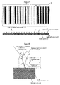
Figs. 5 are a plan view and a side view showing the configuration of a scale according to the present invention; -
Figs. 6 are a plan view and a side view showing a case where the scale is observed at the first optical wavelength; -
Figs. 7 are a plan view and a side view showing a case where the scale is observed at the second optical wavelength; -
Fig. 8 is a sectional view showing interference of light emitted from a dielectric substance layer for description of the principle of the present invention; -
Fig. 9 is a view showing an example of emission light quantity from a dielectric substance layer for description of the principle of the present invention; -
Fig. 10 is a view showing a process for producing a scale by an etching method according to the present invention; -
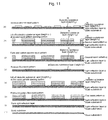
Fig. 11 is a view showing a process for producing a scale by a lift-off method according to the present invention; -
Fig. 12 is a perspective view showing the entire configuration of an embodiment of a reflection type encoder according to the present invention; -
Fig. 13 is a sectional view showing a detailed configuration thereof, -
Fig. 14 is a plan view when the detection head thereof is observed in the Z-axis direction; and -
Fig. 15 is a flowchart showing a method for controlling the light source in the embodiment. - Hereinafter, a detailed description is given of an embodiment of the present invention.
- A scale used in the present embodiment separates an INC pattern and an ABS pattern from each other by controlling the thickness (heights) h1 and h2 of a
dielectric substance layer 34 formed on alight reflection layer 32 formed on ascale substrate 30. For example, a pattern in which the thickness of the dielectric substance layer is h1 can be made into anINC pattern 36, and a pattern in which the thickness of the dielectric substance layer is h2 can be made into anABS pattern 38. - For example, silicon oxide (SiO2), chrome oxide (Cr2O3), titanium nitride (TiN), etc., may be used as a material of the
dielectric substance layer 34. Since a difference in thickness of the dielectric substance layer can be increased if silicon oxide is used, light separation can be facilitated, and a high-performance encoder can be attained. On the other hand, since the refractive index n of chrome oxide or titanium nitride is larger than that of silicon oxide, the thickness h1 or h2 is made smaller, where it becomes difficult to separate light although the cost thereof is decreased. - Where light is reflected through the dielectric substance layer, it has been known that light reflected from the surface layer of the dielectric substance layer interferes with light reflected by the light reflection layer in the dielectric substance layer and darkness is brought about at a specified optical wavelength. Therefore, for example, where it is assumed that the dielectric substance layer of thickness h1 becomes dark when being observed at optical wavelength λ1 and the dielectric substance layer of thickness h2 becomes dark when being observed at optical wavelength λ2, the
patterns Fig. 5 can be observed at the respective optical wavelengths as shown inFig. 6 andFig. 7 . - Interference of light emitted from the dielectric substance layer attenuates where a difference in optical paths of light reflected from the surface of the dielectric substance layer and light reflected from the surface of the reflection layer inside the dielectric substance layer is half the optical wavelength, and is intensified where the difference is equivalent to an integral multiple. That is, according to Snell's law,

- Here, n1 is a refractive index of the dielectric substance layer, no is a refractive index of the atmospheric air layer, θ0 is an incident angle from the atmospheric air layer into the dielectric substance layer, and θ1 is a refractive angle thereof.
- The distances among respective points A, B, C and D are expressed by the following expressions.
-


- Here, h is a thickness (height) of the dielectric substance layer. Therefore, the optical distance between A and C is expressed by the following expression.
-

- Also, the optical distance between A and D is expressed by the following expression.
-

- Therefore, a difference in optical paths is expressed by the following expression.
-

- Here,
Fig. 9 shows the relationship between the height h of the dielectric substance layer and the emission light intensity where n0=1, n1=1.55 (example of SiO2), θ0=15°, λ1=880nm, λ2=660nm, and the reflectance of the respective sides is ideal (ηD=50%, ηR=100%), and where it is assumed that there is no attenuation in the layer. Based onFig. 9 , if 430nm is selected as h1, the emission light quantity of optical wavelength λ2 (660nm) can be maximized when the emission light quantity of optical wavelength λ1 (880nm) is the minimum, and if 330nm is selected as h2, the emission light quantity of optical wavelength λ1 (880nm) can be almost maximized when the emission light quantity of optical wavelength λ2 (660nm) is the minimum. By such selection, the influences by respective wavelengths can be minimized when observing at the respective wavelengths. - Here, patterns having a dielectric substance layer of different height may be produced by a lithography process in which the height of the dielectric substance layer is controlled by an etching method as shown in, for example,
Fig. 10 . - That is, first, (1) a
scale substrate 30 is prepared, (2) alight reflection layer 32 is formed on thescale substrate 30, (3) adielectric substance layer 34 of height h1 is formed thereon, (4) the first resistpattern 40 is formed thereon, and patterned, (5) the dielectric substance layer at the opening portion of the first resistpattern 40 is etched up to height h2, next, (6) the second resistpattern 42 is formed and patterned, next, (7) the dielectric substance layer at the opening portion of the second resistpattern 42 is etched, and finally (8) the second resistpattern 42 is removed. Thus, a scale may be produced. - According to the method, one-time film formation is sufficient to form the scale, wherein the production cost is inexpensive.
- Or, as shown in
Fig. 11 , the scalemaybeproducedby a lithography process in which the height of the dielectric substance layer is controlled by a lift-off method. - That is, first, (1) a
scale substrate 30 is prepared, (2) alight reflection layer 32 is formed on thescale substrate 30, (3) the first resistpattern 40 is formed and patterned thereon, (4) a dielectric substance layer of height h2 is lifted off at the opening portion of the first resistpattern 40, next, (5) the first resistpattern 40 is removed, (6) the second resistpattern 42 is formed and patterned thereon, next (7) a dielectric substance layer of height h1 is lifted off at the opening portion of the second resistpattern 42, and finally (8) the second resistpattern 42 is removed. - According to the method, since there is no process of scraping the surface, the surface is not roughened, wherein interference based on regular reflection can be made secure.
- A reflection type encoder using a scale according to the present invention is composed, as shown in
Fig. 12 , of ascale 28 and adetection head 60 relatively moving thereon in the measurement axis (X-axis) direction. - The
detection head 60 is provided, as shown in detail inFig. 13 (sectional view) and inFig. 14 (plan view), with thefirst light source 62 of optical wavelength λ1, the secondlight source 64 of optical wavelength λ2, a 50:50beam splitter 66 for synthesizing the optical paths of twolight sources beam splitter 66 passes, and a light-receivingelement 74, which is connected to awiring pattern 70, for example, on the COG glass substrate 68 by aconnection bump 72 and is common to two optical wavelengths λ1 and λ2, for detecting light transmitted through the COG glass substrate 68 and reflected by the pattern of thescale 28. - In the present embodiment, the optical path of the first light source 62 (wavelength λ1) and the optical path of the second light source (wavelength λ2) are synthesized by the
beam splitter 66 and reach thedielectric substance layer 34 on thescale substrate 30. The light reflected there is detected by the light-receivingelement 74 connected to thewiring pattern 70 of the COG glass substrate 68 by theconnection bump 72. The detection signal is transmitted to a control circuit portion (not illustrated) through theconnection bump 72 and thewiring pattern 70. - Here, the
light sources Fig. 15 . That is, since the present position is not clear when the power of the encoder is turned on (Step 100), it is necessary to read theABS pattern 38 and to detect the ABS data. Therefore, the secondlight source 64 is lit (Step 110). At this time, thefirst light source 62 remains unlit. - After the ABS data is detected (Step 120), the data is preset in a position counter (Step 130), and the second
light source 64 is unlit (Step 140). - Next, the
first light source 62 is lit (Step 150), and an INC signal is detected (Step 160). A change in the position thereafter is detected by counting the INC signal by means of a position counter (Step 170). - Since the reliability of the position counter data thereafter is lowered where there is any abnormality in the INC signal, for example, a lowering in the signal intensity, during measurement of the INC signal (Step 180), the
first light source 52 is unlit (Step 190), and a routine of detecting the ABS data is re-started (Steps 110 through 140). - As described above, since the ABS data and the INC signal can be detected by a single light-receiving
element 74, the configuration can be downsized. Also, as shown inFig. 14 , the detection center axis of theABS pattern 38 is in agreement with the detection center axis of theINCpattern 36. Therefore, since the ABS detection position and INC detection position on the scale can be made into the same position, there is no case where the ABS data position deviates from the INC signal position, wherein there is no case where both detect different positions, and therefore the reliability of position detection is improved. - In addition, in the above-described embodiment, although the INC pattern and the ABS pattern are formed on a single track, the number of patterns formed on a single track and combination thereof are not limited thereto. For example, two types of ABS patterns or INC patterns may be combined or three or more types of patterns may be combined.
- The present invention may be applicable to a photoelectric type encoder such as a linear encoder and a rotary encoder, and can downsize the scale thereof by overlapping a plurality of patterns such as INC patterns and ABS patterns on the same track.
Claims (10)
- A reflection type encoder, which receives a plurality of light-receiving signals from a single scale, including:a light source;a scale having a plurality of patterns formed thereon to which light is irradiated from the light source; anda light-receiving element for receiving light reflected from each of the plurality of patterns;wherein a plurality of patterns each having different thicknesses are formed on a single track of the scale by using a dielectric substance, light of a plurality of wavelengths each having different brightnesses in accordance with differences in the thickness of the dielectric substance is irradiated from the light source, and a light-receiving signal is obtained for the respective thicknesses of the dielectric substance.
- The reflection type encoder according to Claim 1, wherein the encoder detects a first pattern at a first optical wavelength at which reflection light attenuates by a dielectric substance layer of a first thickness, and detects a second pattern at a second optical wavelength at which reflection light attenuates by a dielectric substance layer of a second thickness.
- The reflection type encoder according to Claim 2, wherein a height of the dielectric substance layer is set so that the light quantity from the dielectric substance layer is minimized at the first optical wavelength and the light quantity from the dielectric substance layer is maximized at the second optical wavelength.
- The reflection type encoder according to any one of Claims 1 through 3, wherein the plurality of patterns are an incremental pattern and an ABS pattern.
- The reflection type encoder according to any one of Claims 1 through 4, wherein the dielectric substance is silicon oxide.
- The reflection type encoder according to Claim 5, wherein the thicknesses of the dielectric substance are 430nm and 330nm, and the wavelengths of the light source are 880nm and 660nm.
- The reflection type encoder according to any one of Claims 1 through 6, wherein the detection center axis of the light-receiving element for detecting the incremental pattern is in agreement with the detection center axis of the light-receiving element for detecting the ABS pattern on the measurement axis.
- A scale of a reflection type encoder, which has a plurality of patterns each having different thicknesses formed on a single track thereof using a dielectric substance.
- A method for producing a scale, comprising the steps of, when forming a plurality of patterns each having different thicknesses on a single track of the scale by using a dielectric substance:forming a light reflection pattern on a scale substrate;forming a dielectric substance layer with a first height thereon;forming and patterning a first resist pattern thereon;etching the dielectric substance layer of the first resist pattern opening portion up to a second height;forming and patterning a second resist pattern thereon;etching the dielectric substance layer of the second resist pattern opening portion; andremoving the second resist pattern.
- A method for producing a scale, comprising the steps of, when forming a plurality of patterns each having different thicknesses on a single track of the scale by using a dielectric substance:forming a light reflection layer on a scale substrate;forming and patterning a first resist pattern thereon;lifting off a dielectric substance layer of a second height at the first resist pattern opening portion;removing the first resist pattern;forming and patterning a second resist pattern thereon;lifting off a dielectric substance layer of a first height at the second resist pattern opening portion; andremoving the second resist pattern.
Applications Claiming Priority (1)
| Application Number | Priority Date | Filing Date | Title |
|---|---|---|---|
| PCT/JP2007/061222 WO2008146409A1 (en) | 2007-06-01 | 2007-06-01 | Reflective encoder, scale thereof, and method for manufacturing scale |
Publications (3)
| Publication Number | Publication Date |
|---|---|
| EP2051047A1 true EP2051047A1 (en) | 2009-04-22 |
| EP2051047A4 EP2051047A4 (en) | 2017-04-19 |
| EP2051047B1 EP2051047B1 (en) | 2019-12-25 |
Family
ID=40074691
Family Applications (1)
| Application Number | Title | Priority Date | Filing Date |
|---|---|---|---|
| EP07744609.4A Active EP2051047B1 (en) | 2007-06-01 | 2007-06-01 | Reflective encoder, scale thereof, and method for manufacturing scale |
Country Status (5)
| Country | Link |
|---|---|
| US (1) | US8127993B2 (en) |
| EP (1) | EP2051047B1 (en) |
| JP (1) | JP4828612B2 (en) |
| CN (1) | CN101484780B (en) |
| WO (1) | WO2008146409A1 (en) |
Cited By (3)
| Publication number | Priority date | Publication date | Assignee | Title |
|---|---|---|---|---|
| EP2551646A3 (en) * | 2011-07-26 | 2013-06-26 | Canon Kabushiki Kaisha | Scale and manufacturing method thereof, and absolute encoder |
| EP3048426A1 (en) * | 2015-01-26 | 2016-07-27 | Dr. Johannes Heidenhain GmbH | Position measurement device |
| US9945697B2 (en) | 2013-01-15 | 2018-04-17 | Renishaw Plc | Measurement scale with periodic nanostructure |
Families Citing this family (16)
| Publication number | Priority date | Publication date | Assignee | Title |
|---|---|---|---|---|
| JP5472986B2 (en) * | 2009-12-29 | 2014-04-16 | 株式会社リガク | Angle measuring device, method of manufacturing angle measuring device, and X-ray analyzer |
| JP5379761B2 (en) * | 2010-08-06 | 2013-12-25 | キヤノン株式会社 | Absolute encoder |
| JP5695478B2 (en) * | 2011-04-15 | 2015-04-08 | Dmg森精機株式会社 | Optical displacement measuring device |
| CN104094087B (en) * | 2011-12-28 | 2016-07-20 | 株式会社尼康 | Encoder, scale for encoder manufacture method, encoder manufacture method and driving device |
| EP2592392B1 (en) | 2012-03-09 | 2013-09-04 | Hexagon Technology Center GmbH | Optoelectronic positioning device |
| EP2884239B1 (en) * | 2013-12-13 | 2016-09-28 | The Swatch Group Research and Development Ltd. | Angular and axial position sensor arrangement |
| JP6366274B2 (en) * | 2014-01-07 | 2018-08-01 | キヤノン株式会社 | Scale, measuring apparatus, image forming apparatus, scale processing apparatus, and scale processing method |
| JP6472166B2 (en) * | 2014-01-20 | 2019-02-20 | キヤノン株式会社 | Position control apparatus and method |
| WO2015147756A1 (en) * | 2014-03-27 | 2015-10-01 | Heptagon Micro Optics Pte. Ltd. | Optical encoder system |
| TWI512272B (en) * | 2014-10-17 | 2015-12-11 | China Steel Corp | Reflective coding system and its encoding method |
| JP5925365B1 (en) * | 2015-05-13 | 2016-05-25 | 株式会社メルテック | Grating plate for optical encoder and manufacturing method of grating plate for optical encoder |
| DE102016204313A1 (en) * | 2016-03-16 | 2017-09-21 | Dr. Johannes Heidenhain Gesellschaft Mit Beschränkter Haftung | Optical distance sensor and position measuring device with such a distance sensor |
| JP6932983B2 (en) * | 2017-05-01 | 2021-09-08 | セイコーエプソン株式会社 | Encoder Scales, Encoder Scale Manufacturing Methods, Encoders, Robots and Printers |
| JP7391527B2 (en) | 2019-04-03 | 2023-12-05 | 株式会社ミツトヨ | photoelectric encoder |
| JP7248504B2 (en) * | 2019-05-30 | 2023-03-29 | 株式会社ミツトヨ | optical encoder |
| CN110686712A (en) * | 2019-11-22 | 2020-01-14 | 中国科学院长春光学精密机械与物理研究所 | Reflective image photoelectric encoder |
Family Cites Families (20)
| Publication number | Priority date | Publication date | Assignee | Title |
|---|---|---|---|---|
| US4286871A (en) * | 1980-08-11 | 1981-09-01 | Keuffel & Esser Company | Photogrammetric measuring system |
| DE3147985C2 (en) | 1981-12-04 | 1986-03-13 | Dr. Johannes Heidenhain Gmbh, 8225 Traunreut | Process for the production of a recording medium with a multicolored fine structure |
| JPS61161616A (en) * | 1985-01-10 | 1986-07-22 | 株式会社東芝 | Bushing remover |
| JPS61161616U (en) * | 1985-03-28 | 1986-10-07 | ||
| GB8522202D0 (en) * | 1985-09-06 | 1985-10-09 | Univ Liverpool | Determining displacement |
| GB8909788D0 (en) * | 1989-04-28 | 1989-06-14 | Renishaw Plc | Optical metrological scale |
| DE9007559U1 (en) * | 1990-03-13 | 1992-09-24 | Dr. Johannes Heidenhain Gmbh, 8225 Traunreut | |
| JPH05118876A (en) * | 1991-10-28 | 1993-05-14 | Tamagawa Seiki Co Ltd | Optical fiber encoder |
| US5838653A (en) * | 1995-10-04 | 1998-11-17 | Reveo, Inc. | Multiple layer optical recording media and method and system for recording and reproducing information using the same |
| DE19941318A1 (en) | 1999-08-31 | 2001-03-15 | Heidenhain Gmbh Dr Johannes | Optical position measuring device |
| DE10011872A1 (en) * | 2000-03-10 | 2001-09-27 | Heidenhain Gmbh Dr Johannes | Reflection measurement graduation and method for producing the same |
| GB0109057D0 (en) | 2001-04-11 | 2001-05-30 | Renishaw Plc | Absolute postition measurement |
| JP2002318137A (en) * | 2001-04-20 | 2002-10-31 | Mitsutoyo Corp | Scale of displacement measuring device |
| JP4250894B2 (en) * | 2001-12-28 | 2009-04-08 | 富士ゼロックス株式会社 | Optical encoder and encoder scale |
| JP2003279381A (en) | 2002-01-21 | 2003-10-02 | Mitsubishi Electric Corp | Encoder code plate, encoder, method of manufacturing mold for encoder code plate, and method of manufacturing encoder code plate |
| JP4332514B2 (en) * | 2002-01-21 | 2009-09-16 | 三菱電機株式会社 | Encoder code plate, encoder, mold manufacturing method for encoder code plate, mold for encoder code plate, and manufacturing method of encoder code plate |
| JP2004037341A (en) * | 2002-07-05 | 2004-02-05 | Mitsutoyo Corp | Manufacturing method of photoelectric encoder and scale |
| CN100397045C (en) * | 2004-01-26 | 2008-06-25 | 三丰株式会社 | Photoelectric encoder and method of manufacturing scales |
| US7256938B2 (en) * | 2004-03-17 | 2007-08-14 | General Atomics | Method for making large scale multilayer dielectric diffraction gratings on thick substrates using reactive ion etching |
| DE102007024349A1 (en) * | 2007-05-24 | 2008-11-27 | Dr. Johannes Heidenhain Gmbh | Optical position measuring device |
-
2007
- 2007-06-01 JP JP2008549697A patent/JP4828612B2/en not_active Expired - Fee Related
- 2007-06-01 EP EP07744609.4A patent/EP2051047B1/en active Active
- 2007-06-01 CN CN2007800248626A patent/CN101484780B/en not_active Expired - Fee Related
- 2007-06-01 WO PCT/JP2007/061222 patent/WO2008146409A1/en not_active Ceased
- 2007-06-01 US US12/227,431 patent/US8127993B2/en not_active Expired - Fee Related
Non-Patent Citations (1)
| Title |
|---|
| See references of WO2008146409A1 * |
Cited By (4)
| Publication number | Priority date | Publication date | Assignee | Title |
|---|---|---|---|---|
| EP2551646A3 (en) * | 2011-07-26 | 2013-06-26 | Canon Kabushiki Kaisha | Scale and manufacturing method thereof, and absolute encoder |
| US9945697B2 (en) | 2013-01-15 | 2018-04-17 | Renishaw Plc | Measurement scale with periodic nanostructure |
| EP3048426A1 (en) * | 2015-01-26 | 2016-07-27 | Dr. Johannes Heidenhain GmbH | Position measurement device |
| US9677874B2 (en) | 2015-01-26 | 2017-06-13 | Dr. Johannes Heidenhain Gmbh | Position-measuring device |
Also Published As
| Publication number | Publication date |
|---|---|
| CN101484780A (en) | 2009-07-15 |
| JP4828612B2 (en) | 2011-11-30 |
| WO2008146409A1 (en) | 2008-12-04 |
| US8127993B2 (en) | 2012-03-06 |
| US20090316155A1 (en) | 2009-12-24 |
| JPWO2008146409A1 (en) | 2010-08-19 |
| EP2051047A4 (en) | 2017-04-19 |
| CN101484780B (en) | 2011-07-06 |
| EP2051047B1 (en) | 2019-12-25 |
Similar Documents
| Publication | Publication Date | Title |
|---|---|---|
| EP2051047B1 (en) | Reflective encoder, scale thereof, and method for manufacturing scale | |
| EP1557701B1 (en) | Photoelectric encoder and method of manufacturing scales | |
| EP1410435B1 (en) | Lateral shift measurement using an optical technique | |
| EP1916505B1 (en) | Photoelectric encoder, scale and method of manufacturing scale | |
| JP4021382B2 (en) | Optical encoder, method of manufacturing the same, and optical lens module | |
| US7800761B2 (en) | Infrared interferometric-spatial-phase imaging using backside wafer marks | |
| EP2946176B1 (en) | Measurement scale comprising a periodic nanostructure | |
| US20130112860A1 (en) | Reflective optical scale for encoder and reflective optical encoder | |
| TW202142837A (en) | Reflection type optical scale for encoder and reflection type optical encoder | |
| JP4913345B2 (en) | Reflective photoelectric encoder scale, scale manufacturing method, and photoelectric encoder | |
| JP7675868B2 (en) | FP sensor probe, absolute distance measuring device, and absolute distance measuring method | |
| US10018485B2 (en) | Scale and position-measuring device having such a scale | |
| US6970255B1 (en) | Encoder measurement based on layer thickness | |
| JP6694722B2 (en) | Optical encoder and its origin determination method | |
| JP2000028484A (en) | Method and apparatus for measuring optical constant of thin film | |
| KR100945314B1 (en) | Shape Measuring Device, Exposure Device and Computer | |
| JP4008893B2 (en) | Encoder | |
| JP2004037341A (en) | Manufacturing method of photoelectric encoder and scale | |
| JP3808192B2 (en) | Movement amount measuring apparatus and movement amount measuring method | |
| JP4615914B2 (en) | Differential pressure measurement system and differential pressure measurement method | |
| JP4331899B2 (en) | Optical encoder |
Legal Events
| Date | Code | Title | Description |
|---|---|---|---|
| PUAI | Public reference made under article 153(3) epc to a published international application that has entered the european phase |
Free format text: ORIGINAL CODE: 0009012 |
|
| 17P | Request for examination filed |
Effective date: 20090302 |
|
| AK | Designated contracting states |
Kind code of ref document: A1 Designated state(s): AT BE BG CH CY CZ DE DK EE ES FI FR GB GR HU IE IS IT LI LT LU LV MC MT NL PL PT RO SE SI SK TR |
|
| AX | Request for extension of the european patent |
Extension state: AL BA HR MK RS |
|
| DAX | Request for extension of the european patent (deleted) | ||
| RA4 | Supplementary search report drawn up and despatched (corrected) |
Effective date: 20170320 |
|
| RIC1 | Information provided on ipc code assigned before grant |
Ipc: G01D 5/347 20060101ALI20170311BHEP Ipc: G01D 5/30 20060101AFI20170311BHEP |
|
| GRAP | Despatch of communication of intention to grant a patent |
Free format text: ORIGINAL CODE: EPIDOSNIGR1 |
|
| STAA | Information on the status of an ep patent application or granted ep patent |
Free format text: STATUS: GRANT OF PATENT IS INTENDED |
|
| INTG | Intention to grant announced |
Effective date: 20190730 |
|
| GRAS | Grant fee paid |
Free format text: ORIGINAL CODE: EPIDOSNIGR3 |
|
| GRAA | (expected) grant |
Free format text: ORIGINAL CODE: 0009210 |
|
| STAA | Information on the status of an ep patent application or granted ep patent |
Free format text: STATUS: THE PATENT HAS BEEN GRANTED |
|
| AK | Designated contracting states |
Kind code of ref document: B1 Designated state(s): AT BE BG CH CY CZ DE DK EE ES FI FR GB GR HU IE IS IT LI LT LU LV MC MT NL PL PT RO SE SI SK TR |
|
| REG | Reference to a national code |
Ref country code: GB Ref legal event code: FG4D |
|
| REG | Reference to a national code |
Ref country code: CH Ref legal event code: EP |
|
| REG | Reference to a national code |
Ref country code: AT Ref legal event code: REF Ref document number: 1217618 Country of ref document: AT Kind code of ref document: T Effective date: 20200115 |
|
| REG | Reference to a national code |
Ref country code: DE Ref legal event code: R096 Ref document number: 602007059665 Country of ref document: DE |
|
| REG | Reference to a national code |
Ref country code: IE Ref legal event code: FG4D |
|
| REG | Reference to a national code |
Ref country code: NL Ref legal event code: MP Effective date: 20191225 |
|
| PG25 | Lapsed in a contracting state [announced via postgrant information from national office to epo] |
Ref country code: SE Free format text: LAPSE BECAUSE OF FAILURE TO SUBMIT A TRANSLATION OF THE DESCRIPTION OR TO PAY THE FEE WITHIN THE PRESCRIBED TIME-LIMIT Effective date: 20191225 Ref country code: LV Free format text: LAPSE BECAUSE OF FAILURE TO SUBMIT A TRANSLATION OF THE DESCRIPTION OR TO PAY THE FEE WITHIN THE PRESCRIBED TIME-LIMIT Effective date: 20191225 Ref country code: FI Free format text: LAPSE BECAUSE OF FAILURE TO SUBMIT A TRANSLATION OF THE DESCRIPTION OR TO PAY THE FEE WITHIN THE PRESCRIBED TIME-LIMIT Effective date: 20191225 Ref country code: BG Free format text: LAPSE BECAUSE OF FAILURE TO SUBMIT A TRANSLATION OF THE DESCRIPTION OR TO PAY THE FEE WITHIN THE PRESCRIBED TIME-LIMIT Effective date: 20200325 Ref country code: GR Free format text: LAPSE BECAUSE OF FAILURE TO SUBMIT A TRANSLATION OF THE DESCRIPTION OR TO PAY THE FEE WITHIN THE PRESCRIBED TIME-LIMIT Effective date: 20200326 Ref country code: LT Free format text: LAPSE BECAUSE OF FAILURE TO SUBMIT A TRANSLATION OF THE DESCRIPTION OR TO PAY THE FEE WITHIN THE PRESCRIBED TIME-LIMIT Effective date: 20191225 |
|
| REG | Reference to a national code |
Ref country code: LT Ref legal event code: MG4D |
|
| PG25 | Lapsed in a contracting state [announced via postgrant information from national office to epo] |
Ref country code: EE Free format text: LAPSE BECAUSE OF FAILURE TO SUBMIT A TRANSLATION OF THE DESCRIPTION OR TO PAY THE FEE WITHIN THE PRESCRIBED TIME-LIMIT Effective date: 20191225 Ref country code: PT Free format text: LAPSE BECAUSE OF FAILURE TO SUBMIT A TRANSLATION OF THE DESCRIPTION OR TO PAY THE FEE WITHIN THE PRESCRIBED TIME-LIMIT Effective date: 20200520 Ref country code: NL Free format text: LAPSE BECAUSE OF FAILURE TO SUBMIT A TRANSLATION OF THE DESCRIPTION OR TO PAY THE FEE WITHIN THE PRESCRIBED TIME-LIMIT Effective date: 20191225 Ref country code: CZ Free format text: LAPSE BECAUSE OF FAILURE TO SUBMIT A TRANSLATION OF THE DESCRIPTION OR TO PAY THE FEE WITHIN THE PRESCRIBED TIME-LIMIT Effective date: 20191225 Ref country code: RO Free format text: LAPSE BECAUSE OF FAILURE TO SUBMIT A TRANSLATION OF THE DESCRIPTION OR TO PAY THE FEE WITHIN THE PRESCRIBED TIME-LIMIT Effective date: 20191225 |
|
| PGFP | Annual fee paid to national office [announced via postgrant information from national office to epo] |
Ref country code: DE Payment date: 20200618 Year of fee payment: 14 |
|
| PG25 | Lapsed in a contracting state [announced via postgrant information from national office to epo] |
Ref country code: IS Free format text: LAPSE BECAUSE OF FAILURE TO SUBMIT A TRANSLATION OF THE DESCRIPTION OR TO PAY THE FEE WITHIN THE PRESCRIBED TIME-LIMIT Effective date: 20200425 Ref country code: SK Free format text: LAPSE BECAUSE OF FAILURE TO SUBMIT A TRANSLATION OF THE DESCRIPTION OR TO PAY THE FEE WITHIN THE PRESCRIBED TIME-LIMIT Effective date: 20191225 |
|
| PGFP | Annual fee paid to national office [announced via postgrant information from national office to epo] |
Ref country code: GB Payment date: 20200625 Year of fee payment: 14 |
|
| REG | Reference to a national code |
Ref country code: DE Ref legal event code: R097 Ref document number: 602007059665 Country of ref document: DE |
|
| PG25 | Lapsed in a contracting state [announced via postgrant information from national office to epo] |
Ref country code: DK Free format text: LAPSE BECAUSE OF FAILURE TO SUBMIT A TRANSLATION OF THE DESCRIPTION OR TO PAY THE FEE WITHIN THE PRESCRIBED TIME-LIMIT Effective date: 20191225 Ref country code: ES Free format text: LAPSE BECAUSE OF FAILURE TO SUBMIT A TRANSLATION OF THE DESCRIPTION OR TO PAY THE FEE WITHIN THE PRESCRIBED TIME-LIMIT Effective date: 20191225 |
|
| PLBE | No opposition filed within time limit |
Free format text: ORIGINAL CODE: 0009261 |
|
| STAA | Information on the status of an ep patent application or granted ep patent |
Free format text: STATUS: NO OPPOSITION FILED WITHIN TIME LIMIT |
|
| REG | Reference to a national code |
Ref country code: AT Ref legal event code: MK05 Ref document number: 1217618 Country of ref document: AT Kind code of ref document: T Effective date: 20191225 |
|
| PG25 | Lapsed in a contracting state [announced via postgrant information from national office to epo] |
Ref country code: SI Free format text: LAPSE BECAUSE OF FAILURE TO SUBMIT A TRANSLATION OF THE DESCRIPTION OR TO PAY THE FEE WITHIN THE PRESCRIBED TIME-LIMIT Effective date: 20191225 |
|
| 26N | No opposition filed |
Effective date: 20200928 |
|
| PG25 | Lapsed in a contracting state [announced via postgrant information from national office to epo] |
Ref country code: AT Free format text: LAPSE BECAUSE OF FAILURE TO SUBMIT A TRANSLATION OF THE DESCRIPTION OR TO PAY THE FEE WITHIN THE PRESCRIBED TIME-LIMIT Effective date: 20191225 Ref country code: IT Free format text: LAPSE BECAUSE OF FAILURE TO SUBMIT A TRANSLATION OF THE DESCRIPTION OR TO PAY THE FEE WITHIN THE PRESCRIBED TIME-LIMIT Effective date: 20191225 Ref country code: MC Free format text: LAPSE BECAUSE OF FAILURE TO SUBMIT A TRANSLATION OF THE DESCRIPTION OR TO PAY THE FEE WITHIN THE PRESCRIBED TIME-LIMIT Effective date: 20191225 |
|
| REG | Reference to a national code |
Ref country code: CH Ref legal event code: PL |
|
| PG25 | Lapsed in a contracting state [announced via postgrant information from national office to epo] |
Ref country code: PL Free format text: LAPSE BECAUSE OF FAILURE TO SUBMIT A TRANSLATION OF THE DESCRIPTION OR TO PAY THE FEE WITHIN THE PRESCRIBED TIME-LIMIT Effective date: 20191225 |
|
| PG25 | Lapsed in a contracting state [announced via postgrant information from national office to epo] |
Ref country code: LU Free format text: LAPSE BECAUSE OF NON-PAYMENT OF DUE FEES Effective date: 20200601 |
|
| REG | Reference to a national code |
Ref country code: BE Ref legal event code: MM Effective date: 20200630 |
|
| PG25 | Lapsed in a contracting state [announced via postgrant information from national office to epo] |
Ref country code: LI Free format text: LAPSE BECAUSE OF NON-PAYMENT OF DUE FEES Effective date: 20200630 Ref country code: IE Free format text: LAPSE BECAUSE OF NON-PAYMENT OF DUE FEES Effective date: 20200601 Ref country code: CH Free format text: LAPSE BECAUSE OF NON-PAYMENT OF DUE FEES Effective date: 20200630 Ref country code: FR Free format text: LAPSE BECAUSE OF NON-PAYMENT OF DUE FEES Effective date: 20200630 |
|
| PG25 | Lapsed in a contracting state [announced via postgrant information from national office to epo] |
Ref country code: BE Free format text: LAPSE BECAUSE OF NON-PAYMENT OF DUE FEES Effective date: 20200630 |
|
| REG | Reference to a national code |
Ref country code: DE Ref legal event code: R119 Ref document number: 602007059665 Country of ref document: DE |
|
| GBPC | Gb: european patent ceased through non-payment of renewal fee |
Effective date: 20210601 |
|
| PG25 | Lapsed in a contracting state [announced via postgrant information from national office to epo] |
Ref country code: GB Free format text: LAPSE BECAUSE OF NON-PAYMENT OF DUE FEES Effective date: 20210601 Ref country code: DE Free format text: LAPSE BECAUSE OF NON-PAYMENT OF DUE FEES Effective date: 20220101 |
|
| PG25 | Lapsed in a contracting state [announced via postgrant information from national office to epo] |
Ref country code: TR Free format text: LAPSE BECAUSE OF FAILURE TO SUBMIT A TRANSLATION OF THE DESCRIPTION OR TO PAY THE FEE WITHIN THE PRESCRIBED TIME-LIMIT Effective date: 20191225 Ref country code: MT Free format text: LAPSE BECAUSE OF FAILURE TO SUBMIT A TRANSLATION OF THE DESCRIPTION OR TO PAY THE FEE WITHIN THE PRESCRIBED TIME-LIMIT Effective date: 20191225 Ref country code: CY Free format text: LAPSE BECAUSE OF FAILURE TO SUBMIT A TRANSLATION OF THE DESCRIPTION OR TO PAY THE FEE WITHIN THE PRESCRIBED TIME-LIMIT Effective date: 20191225 |