EP2051307A2 - Method of fast hydrogen passivation to solar cells made of crystalline silicon - Google Patents
Method of fast hydrogen passivation to solar cells made of crystalline silicon Download PDFInfo
- Publication number
- EP2051307A2 EP2051307A2 EP07254367A EP07254367A EP2051307A2 EP 2051307 A2 EP2051307 A2 EP 2051307A2 EP 07254367 A EP07254367 A EP 07254367A EP 07254367 A EP07254367 A EP 07254367A EP 2051307 A2 EP2051307 A2 EP 2051307A2
- Authority
- EP
- European Patent Office
- Prior art keywords
- solar cells
- hydrogen
- solar cell
- passivation
- hydrogen passivation
- Prior art date
- Legal status (The legal status is an assumption and is not a legal conclusion. Google has not performed a legal analysis and makes no representation as to the accuracy of the status listed.)
- Withdrawn
Links
Images

Classifications
-
- H—ELECTRICITY
- H10—SEMICONDUCTOR DEVICES; ELECTRIC SOLID-STATE DEVICES NOT OTHERWISE PROVIDED FOR
- H10F—INORGANIC SEMICONDUCTOR DEVICES SENSITIVE TO INFRARED RADIATION, LIGHT, ELECTROMAGNETIC RADIATION OF SHORTER WAVELENGTH OR CORPUSCULAR RADIATION
- H10F71/00—Manufacture or treatment of devices covered by this subclass
- H10F71/129—Passivating
-
- H—ELECTRICITY
- H10—SEMICONDUCTOR DEVICES; ELECTRIC SOLID-STATE DEVICES NOT OTHERWISE PROVIDED FOR
- H10F—INORGANIC SEMICONDUCTOR DEVICES SENSITIVE TO INFRARED RADIATION, LIGHT, ELECTROMAGNETIC RADIATION OF SHORTER WAVELENGTH OR CORPUSCULAR RADIATION
- H10F71/00—Manufacture or treatment of devices covered by this subclass
- H10F71/121—The active layers comprising only Group IV materials
-
- Y—GENERAL TAGGING OF NEW TECHNOLOGICAL DEVELOPMENTS; GENERAL TAGGING OF CROSS-SECTIONAL TECHNOLOGIES SPANNING OVER SEVERAL SECTIONS OF THE IPC; TECHNICAL SUBJECTS COVERED BY FORMER USPC CROSS-REFERENCE ART COLLECTIONS [XRACs] AND DIGESTS
- Y02—TECHNOLOGIES OR APPLICATIONS FOR MITIGATION OR ADAPTATION AGAINST CLIMATE CHANGE
- Y02E—REDUCTION OF GREENHOUSE GAS [GHG] EMISSIONS, RELATED TO ENERGY GENERATION, TRANSMISSION OR DISTRIBUTION
- Y02E10/00—Energy generation through renewable energy sources
- Y02E10/50—Photovoltaic [PV] energy
- Y02E10/547—Monocrystalline silicon PV cells
-
- Y—GENERAL TAGGING OF NEW TECHNOLOGICAL DEVELOPMENTS; GENERAL TAGGING OF CROSS-SECTIONAL TECHNOLOGIES SPANNING OVER SEVERAL SECTIONS OF THE IPC; TECHNICAL SUBJECTS COVERED BY FORMER USPC CROSS-REFERENCE ART COLLECTIONS [XRACs] AND DIGESTS
- Y02—TECHNOLOGIES OR APPLICATIONS FOR MITIGATION OR ADAPTATION AGAINST CLIMATE CHANGE
- Y02P—CLIMATE CHANGE MITIGATION TECHNOLOGIES IN THE PRODUCTION OR PROCESSING OF GOODS
- Y02P70/00—Climate change mitigation technologies in the production process for final industrial or consumer products
- Y02P70/50—Manufacturing or production processes characterised by the final manufactured product
Definitions
- the present invention relates to a method of hydrogenation of silicon substrates, and more particularly to a fast hydrogenation process to passivate silicon crystal defects in solar cells made of crystalline silicon (c-Si) including monocrystalline silicon (m-Si), multicrystalline silicon (mc-Si), and polycrystalline silicon (poly-Si) thin film.
- c-Si crystalline silicon
- m-Si monocrystalline silicon
- mc-Si multicrystalline silicon
- poly-Si polycrystalline silicon
- Hydrogenated amorphous silicon nitride a-SiN x :H film has become an important application in solar cells, which is deposited on the silicon wafer by PECVD.
- the first purpose of the application of a-SiN x :H film is to function as an antireflection coating. Secondly, it can provide a surface passivation effect, to reduce the recombination of charge carriers at the surface of silicon wafer in solar cells.
- the hydrogen atoms in a-SiN x :H film can diffuse into silicon bulk and passivate the defects of the crystal lattice.
- thermal process is required to raise the temperatures of the solar cells for increasing the diffusion of hydrogen atoms to achieve optimum passivation.
- the operating temperature is around 350 °C and the passivation process usually takes 1 to 2 hours.
- the electrodes are fabricated after completing the antireflection coating. As the fabrication of electrode always needs to perform a step of high-temperature heating and baking, and the bond of hydrogen and silicon will be discomposed above 400°C, and hydrogen atoms will leave the wafer, the effects of hydrogen passivation will be damaged.
- the present invention is directed to provide a method of hydrogen passivation to c-Si solar cells, so as to improve the performance of c-Si solar cells.
- the method can be used to realize a fast hydrogen passivation to alleviate the detrimental effects caused by the defects in silicon crystals. Furthermore, this method must not cause damage to the antireflection coating such as a-SiN x :H films.
- the method of hydrogen passivation of c-Si solar cells can improve the performance of the solar cells which have been completely fabricated.
- the present invention provides a method of hydrogen passivation to c-Si solar cells, which includes the following steps.
- the method of hydrogen passivation to c-Si solar cells includes the following steps. First, a c-Si solar cell wafer is placed in a vacuum chamber, and the solar cell has had an antireflection coating and electrodes. Next, a hydrogen gas is supplied into the vacuum chamber to a predetermined pressure. And then, a RF or microwave power source is transmitted into the vacuum chamber to produce a hydrogen plasma. Afterwards, a negative bias pulse is provided to the solar cell wafer, so as to attract and implant the hydrogen ions therein.
- high-density plasma can provide a high dose rate of hydrogen ions.
- the process time can be significantly reduced.
- the implements of this method are much simpler and more economical in a mass production process.
- the accumulation of implanted charges can be neutralized by electrons from the plasma between negative bias pulses. So, the problem of damages by charging accumulation can be obviated by controlling the pulse width. Meanwhile, the possible deterioration of the antireflection coating by the bombardment of ions can be averted by choosing a proper pulse voltage.
- FIG. 1 is a cross-sectional front view of a typical solar cell.
- FIG. 2 is a schematic view showing the hydrogen possivation to c-Si solar cells of the present invention.
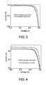
- FIG. 3 is a plot of the electrical characteristics (I-V) of a solar cell made of a multicrystalline silicon illustrated in FIG. 1 before and after hydrogen passivation, under simulated AM1.5 illumination.
- FIG. 4 is a plot of the electrical characteristics (I-V) of a solar cell made of monocrystalline silicon as illustrated in FIG. 1 before and after hydrogen passivation, under simulated AM1.5 illumination.
- FIG. 1 is a typical solar cell 10, which includes a c-Si wafer 100 having a pn junction 104 formed thereon.
- the surface of the wafer has random pyramid textures 13.
- a thin layer of SiO 2 14 grown by thermal process is used to serve as a surface passivation layer 106.
- an antireflection coating 108 of an a-SiN x : H film is deposited by means of PECVD.
- Electrodes 112 and 114 are fabricated respectively on a front surface 100a and a rear surface 110b of the c-Si wafer 100. Additionally, the electrode 114 is generally formed in a dielectric layer 116 deposited on the rear surface 100b of the c-Si wafer 100.
- FIG. 2 is a schematic view showing the hydrogen possivation to a c-Si solar cell wafer 200.
- the c-Si solar cell wafer 200 is placed on a wafer holder 204 in a vacuum chamber 202, and the pressure in the vacuum chamber 202 is reduced to approximately 10 -6 Torr.
- a gas supply equipment 206 supplies hydrogen gas into the vacuum chamber 202 to predetermined pressure, approximately 1-10 mTorr.
- a microwave or RF power is transmitted into the vacuum chamber 202 by a microwave or RF power generator 208, so as to produce a hydrogen plasma.
- the plasma density should be higher than 10 -10 cm -3 to achieve an effective process.
- a negative pulse voltage is provided to the wafer holder 204 by a pulse generator 212 at predetermined voltage, predetermined pulse frequency, and predetermined pulse time width, so as to apply a bias on the c-Si solar cell wafer 200.
- the pulse frequency of the negative pulse voltage is from 100 Hz to 20 kHz.
- the voltage range is from -500 V to -5 kV, so as to ensure the antireflection layer (such as 108 in FIG. 1 ) in the c-Si solar cell wafer 200 will not be damaged during hydrogen passivation.
- the pulse duration of the negative pulse voltage is from I ⁇ sec to 20 ⁇ sec.
- hydrogen ions from a plasma source 210 are accelerated by the negative voltage and implanted into c-Si solar cell wafer 200.
- the period of the process is between 1 to 10 min.
- the temperature of the c-Si solar cell wafer 200 is maintained at approximately 300 to 350°C by an external heating power source.
- the base pressure of the vacuum chamber is 10 -6 Torr, and then hydrogen gas is intruded into the vacuum chamber as a working gas and the pressure is raised to 2 mTorr.
- the plasma is excited by a RF power (13.56 MHz) through an inductive coupling antenna with a power of 200 W.
- the plasma density is approximately 10 11 cm -3 .
- a bias is applied to the solar cell by a pulse voltage of -4 kV.
- the pulse width is 10 ⁇ sec and the pulse frequency is 200 Hz.
- no power supply is provided to heat the solar cell, but the temperatures of the samples are approximately 100°C resulting from the plasma ions implantation.
- the total process time is 10 min.
- Solar cells are fabricated by mc-Si wafers that are p-type, boron doped to 1 x 10 20 cm -3 . Their mean grain size is approximately 5 mm. Random pyramid textures have been made on the front surface of the wafer. N + P junctions are fabricated by diffusion of POCL 3 at 850°C for 20 min. Next, a SiO 2 layer of 20 nm is formed by an oxidized thermal process. Afterwards, an a-SiN x :H film of approximately 90 nm is deposited for antireflection by a capacitively coupled RF plasma reactor at temperature of 350°C, with SiH 4 and NH 3 as precursors. Metallic contacts are made by metal printing and firing at 750°C.
- FIG. 3 is the comparison of current-voltage characteristics the solar cell before and after hydrogen passivation. It is shown by the results that the serious resistance is significantly reduced and the filling factor increases from 76.99% to 81.25%, and the short-circuit current is increased. These improvements lead to an increase of the conversion efficiency from 12.33% to 13.39 %.
- FIG. 4 is the comparison of current-voltage characteristics the solar cell before and after hydrogen passivation. It is shown by the results that the filling factor increases from 75% to 80.77 % as a result. Meanwhile, the short-circuit current increases from 0.23 A to 0.25 A and the open voltage increase from 0.59 V to 0.6 V as well. These improvements lead to an increase of the conversion efficiency from 14.25 % to 17.06 %.
- the present invention can significantly reduce the time and the cost of hydrogen passivation, and effectively improve the efficiency of c-Si solar cells. Furthermore, the implements of this method are simpler and more economical in a mass production process.
- the present invention can be applied to various types of c-Si solar cells. Especially, the present invention can perform hydrogen passivation to the solar cells which fails to meet the requirements for efficiency in the production, so as to improve the efficiency and increase the production yield. In addition, the present invention is not required to change the existing production methods of solar cells, so it is independent process and has high conformability.
Landscapes
- Photovoltaic Devices (AREA)
Abstract
Description
- The present invention relates to a method of hydrogenation of silicon substrates, and more particularly to a fast hydrogenation process to passivate silicon crystal defects in solar cells made of crystalline silicon (c-Si) including monocrystalline silicon (m-Si), multicrystalline silicon (mc-Si), and polycrystalline silicon (poly-Si) thin film.
- Solar cell is a very promising clean energy source which can generate electricity directly from sunlight. However, the cost of the production of solar cells needs to be significantly reduced, so as to be widely accepted as a major electricity source. It has been pointed out that the silicon wafer share is above one third of the total cost of a c-Si solar cell module. Consequently, in order to reduce the cost, making solar cells by mc-Si or poly-Si thin film has been an important development direction. However, both mc-Si and poly-Si contain defects within the crystals, including grain boundary, intragrain dislocations. Those imperfections can degrade the conversion efficiency of solar cells. Besides, the recombination of charge carriers at surfaces of the crystal lattice is detrimental to solar cells, even in the case of monocrystalline solar cells.
- It has been shown that the effects of the crystal defects can be minimized by incorporating hydrogen into silicon wafers, which is called as "passivation" process. As a result, the efficiency of c-Si solar cells can be significantly improved. The general view has been that these efficiency improvements are closely related to the reduction of the charge carrier recombination losses at the crystal defects due to bonds formed by hydrogen ions on the crystal defects. Now, in techniques of manufacturing solar cells, the methods of hydrogen incorporation to alleviate the detrimental effects caused by crystal defects include:
- (1) Heat treatment in hydrogen atmosphere:
- P. Sana, A. Rohatgi, J. P. Kalejs, and R. O. Bell, Appl. Phys. Lett. 64, 97 (1994),
U.S. Pat. No. 5,169,791 ;
- P. Sana, A. Rohatgi, J. P. Kalejs, and R. O. Bell, Appl. Phys. Lett. 64, 97 (1994),
- (2) Treatment with a hydrogen plasma:
- W. Schmidt, K.D. Rasch, and K. Roy, 16 IEEE Photovoltaic Specialist Conference, San Diego, 1982, pages 537-542,
-
U. S. Pat. No. 4,835,006 andU. S. Pat. No. 4,343,830 ;
- (3) Diffusion from hydrogen rich SiNx:H thin film layers deposited by plasma enchanced chemical vapor deposition (PECVD):
- R. Hezel and R. Schroner, J. Appl. Phys., 52(4), 3076 (1981);
- (4) Implantation of ionized hydrogen atoms:
-
U. S. Pat. No. 5,304, 509 , - J. E. Johnson, J. I. Hano Ka, and J. A. Gregory, 18 IEEE Photovoltaic Specialists Conference, Las Vegas 1985, pages 1112-1115.
-
- For the process of hydrogen passivation, sufficient hydrogen atoms are required to form bonds on a plurality of crystal defects. However, because of the limited diffusion of hydrogen atoms through the surface of the wafer, the process time in methods from (1) to (3) is in the order of hours. Meanwhile, the process time can be significantly reduced in method (4), where the hydrogen ions are implanted into a wafer by a conventional Kaufman broad beam ion source. But in practical industrial applications, a plurality set of ion beams of large area is required to meet the mass production of solar cells, and an ion beam source equipment of such specification then becomes an expensive and complicated system. In addition, acceleration electrodes in Kaufman ion beam source are bombarded by ions during the process. The sputtered metal particles may become the source of contamination, which can degrade the performance of solar cellars.
- Hydrogenated amorphous silicon nitride a-SiNx:H film has become an important application in solar cells, which is deposited on the silicon wafer by PECVD. The first purpose of the application of a-SiNx:H film is to function as an antireflection coating. Secondly, it can provide a surface passivation effect, to reduce the recombination of charge carriers at the surface of silicon wafer in solar cells. Additionally, the hydrogen atoms in a-SiNx:H film can diffuse into silicon bulk and passivate the defects of the crystal lattice. For this purpose, thermal process is required to raise the temperatures of the solar cells for increasing the diffusion of hydrogen atoms to achieve optimum passivation. The operating temperature is around 350 °C and the passivation process usually takes 1 to 2 hours.
- In the production of some solar cells, the electrodes are fabricated after completing the antireflection coating. As the fabrication of electrode always needs to perform a step of high-temperature heating and baking, and the bond of hydrogen and silicon will be discomposed above 400°C, and hydrogen atoms will leave the wafer, the effects of hydrogen passivation will be damaged.
- In view of above, there is a need for a fast hydrogen passivation which can significantly reducing the process time in the production of c-Si solar cells. Especially, such process can be performed after the fabrication of c-Si solar cells. In other words, it is a fast hydrogen passivation process that still can be performed after the deposition of the antireflection coating and the fabrication of the electrodes. Furthermore, the implement of this method must be simpler and more adaptable to the mass production process for solar cells, compared with the conventional ion implantation by Kaufman broad beam ion source.
- Accordingly, the present invention is directed to provide a method of hydrogen passivation to c-Si solar cells, so as to improve the performance of c-Si solar cells. The method can be used to realize a fast hydrogen passivation to alleviate the detrimental effects caused by the defects in silicon crystals. Furthermore, this method must not cause damage to the antireflection coating such as a-SiNx:H films. In addition, the method of hydrogen passivation of c-Si solar cells can improve the performance of the solar cells which have been completely fabricated.
- The present invention provides a method of hydrogen passivation to c-Si solar cells, which includes the following steps.
- (a) Place a c-Si solar cell into a vacuum chamber, in which electrodes and an antireflection coating are disposed on the surface of the c-Si solar cell.
- (b) Supply hydrogen gas into the vacuum chamber to a predetermined pressure.
- (c) Transmit a radio frequency (RF) or microwave power into the vacuum chamber to produce a hydrogen plasma.
- (d) Provide a negative pulse bias to the c-Si solar cell wafer by a pulse generator at a predetermined voltage, a predetermined frequency, and a predetermined time width, and implant sufficient hydrogen ions into the c-Si solar cell wafer in a predetermined time period, in which the negative pulse voltage is controlled in a set range to avoid damaging the antireflection coating.
- The method of hydrogen passivation to c-Si solar cells provided by the present invention includes the following steps. First, a c-Si solar cell wafer is placed in a vacuum chamber, and the solar cell has had an antireflection coating and electrodes. Next, a hydrogen gas is supplied into the vacuum chamber to a predetermined pressure. And then, a RF or microwave power source is transmitted into the vacuum chamber to produce a hydrogen plasma. Afterwards, a negative bias pulse is provided to the solar cell wafer, so as to attract and implant the hydrogen ions therein.
- In this method, high-density plasma can provide a high dose rate of hydrogen ions. Compared with the existing techniques, the process time can be significantly reduced. On the other hand, compared with conventional ion beam process, the implements of this method are much simpler and more economical in a mass production process. Meanwhile, the accumulation of implanted charges can be neutralized by electrons from the plasma between negative bias pulses. So, the problem of damages by charging accumulation can be obviated by controlling the pulse width. Meanwhile, the possible deterioration of the antireflection coating by the bombardment of ions can be averted by choosing a proper pulse voltage.
- In order to make the aforementioned and other objects, features and advantages of the present invention comprehensible, preferred embodiments accompanied with figures are described in detail below.
- It is to be understood that both the foregoing general description and the following detailed description are exemplary, and are intended to provide further explanation of the invention as claimed.
- The accompanying drawings are included to provide a further understanding of the invention, and are incorporated in and constitute a part of this specification. The drawings illustrate embodiments of the invention and, together with the description, serve to explain the principles of the invention.
-
FIG. 1 is a cross-sectional front view of a typical solar cell. -
FIG. 2 is a schematic view showing the hydrogen possivation to c-Si solar cells of the present invention. -
FIG. 3 is a plot of the electrical characteristics (I-V) of a solar cell made of a multicrystalline silicon illustrated inFIG. 1 before and after hydrogen passivation, under simulated AM1.5 illumination. -
FIG. 4 is a plot of the electrical characteristics (I-V) of a solar cell made of monocrystalline silicon as illustrated inFIG. 1 before and after hydrogen passivation, under simulated AM1.5 illumination. -
FIG. 1 is a typicalsolar cell 10, which includes a c-Si wafer 100 having apn junction 104 formed thereon. The surface of the wafer has random pyramid textures 13. A thin layer of SiO2 14 grown by thermal process is used to serve as asurface passivation layer 106. And then, anantireflection coating 108 of an a-SiNx: H film is deposited by means of PECVD.Electrodes Si wafer 100. Additionally, theelectrode 114 is generally formed in adielectric layer 116 deposited on therear surface 100b of the c-Si wafer 100. -
FIG. 2 is a schematic view showing the hydrogen possivation to a c-Sisolar cell wafer 200. First, the c-Sisolar cell wafer 200 is placed on awafer holder 204 in avacuum chamber 202, and the pressure in thevacuum chamber 202 is reduced to approximately 10-6 Torr. Next, agas supply equipment 206 supplies hydrogen gas into thevacuum chamber 202 to predetermined pressure, approximately 1-10 mTorr. And then, a microwave or RF power is transmitted into thevacuum chamber 202 by a microwave orRF power generator 208, so as to produce a hydrogen plasma. Generally, the plasma density should be higher than 10-10 cm-3 to achieve an effective process. - After the plasma is excited, a negative pulse voltage is provided to the
wafer holder 204 by apulse generator 212 at predetermined voltage, predetermined pulse frequency, and predetermined pulse time width, so as to apply a bias on the c-Sisolar cell wafer 200. The pulse frequency of the negative pulse voltage is from 100 Hz to 20 kHz. The voltage range is from -500 V to -5 kV, so as to ensure the antireflection layer (such as 108 inFIG. 1 ) in the c-Sisolar cell wafer 200 will not be damaged during hydrogen passivation. And the pulse duration of the negative pulse voltage is from I µsec to 20 µsec. Then, hydrogen ions from aplasma source 210 are accelerated by the negative voltage and implanted into c-Sisolar cell wafer 200. The period of the process is between 1 to 10 min. Additionally, during implanting the hydrogen ions, the temperature of the c-Sisolar cell wafer 200 is maintained at approximately 300 to 350°C by an external heating power source. - The following examples will illustrate the effects of hydrogen passivation of the present invention.
- Example 1
- In this example, the base pressure of the vacuum chamber is 10-6 Torr, and then hydrogen gas is intruded into the vacuum chamber as a working gas and the pressure is raised to 2 mTorr. The plasma is excited by a RF power (13.56 MHz) through an inductive coupling antenna with a power of 200 W. The plasma density is approximately 1011 cm-3. Furthermore, a bias is applied to the solar cell by a pulse voltage of -4 kV. The pulse width is 10 µsec and the pulse frequency is 200 Hz. In this experiment, no power supply is provided to heat the solar cell, but the temperatures of the samples are approximately 100°C resulting from the plasma ions implantation. The total process time is 10 min.
- Solar cells are fabricated by mc-Si wafers that are p-type, boron doped to 1 x 1020 cm-3. Their mean grain size is approximately 5 mm. Random pyramid textures have been made on the front surface of the wafer. N+P junctions are fabricated by diffusion of POCL3 at 850°C for 20 min. Next, a SiO2 layer of 20 nm is formed by an oxidized thermal process. Afterwards, an a-SiNx:H film of approximately 90 nm is deposited for antireflection by a capacitively coupled RF plasma reactor at temperature of 350°C, with SiH4 and NH3 as precursors. Metallic contacts are made by metal printing and firing at 750°C.
-
FIG. 3 is the comparison of current-voltage characteristics the solar cell before and after hydrogen passivation. It is shown by the results that the serious resistance is significantly reduced and the filling factor increases from 76.99% to 81.25%, and the short-circuit current is increased. These improvements lead to an increase of the conversion efficiency from 12.33% to 13.39 %. - Example 2
- In this example, a solar cell made of a monocrystalline silicon wafer is fabricated. The structure and the process of the fabrication are as same as in example 1. In addition, the plasma condition and treatment conditions are also the same.
FIG. 4 is the comparison of current-voltage characteristics the solar cell before and after hydrogen passivation. It is shown by the results that the filling factor increases from 75% to 80.77 % as a result. Meanwhile, the short-circuit current increases from 0.23 A to 0.25 A and the open voltage increase from 0.59 V to 0.6 V as well. These improvements lead to an increase of the conversion efficiency from 14.25 % to 17.06 %. - In view of above, compared with the existing techniques, the present invention can significantly reduce the time and the cost of hydrogen passivation, and effectively improve the efficiency of c-Si solar cells. Furthermore, the implements of this method are simpler and more economical in a mass production process. The present invention can be applied to various types of c-Si solar cells. Especially, the present invention can perform hydrogen passivation to the solar cells which fails to meet the requirements for efficiency in the production, so as to improve the efficiency and increase the production yield. In addition, the present invention is not required to change the existing production methods of solar cells, so it is independent process and has high conformability.
- It will be apparent to those skilled in the art that various modifications and variations can be made to the structure of the present invention without departing from the scope or spirit of the invention. In view of the foregoing, it is intended that the present invention cover modifications and variations of this invention provided they fall within the scope of the following claims and their equivalents.
Claims (6)
- A method of hydrogen passivation to c-Si solar cells, comprising:(a) placing a c-Si solar cell wafer into a vacuum chamber, wherein electrodes and an antireflection coating are disposed on a surface of the c-Si solar cell wafer;(b) supplying a hydrogen gas into the vacuum chamber to a predetermined pressure;(c) transmitting a radio frequency (RF) or a microwave power into the vacuum chamber to produce a hydrogen plasma; and(d) providing a negative pulse voltage to the c-Si solar cell wafer by a pulse generator at a predetermined voltage, a predetermined frequency, and a predetermined time width, and implanting sufficient hydrogen ions into the c-Si solar cell wafer in a period of the process, wherein the negative pulse voltage is controlled in a set range to avoid damaging the antireflection coating.
- The method of hydrogen passivation to c-Si solar cells as claimed in claim 1, wherein the negative pulse voltage is between -500 V and -10 kV.
- The method of hydrogen passivation to c-Si solar cells as claimed in claim 1, wherein the time for supplying the negative pulse voltage is between 1 µsec and 20 µsec.
- The method of hydrogen passivation to c-Si solar cells as claimed in claim 1, wherein the pulse frequency is between 100 Hz and 20 kHz.
- The method of hydrogen passivation to c-Si solar cells as claimed in claim 1, wherein the period of the process is between 1 min and 10 min.
- The method of hydrogen passivation to c-Si solar cells as claimed in claim 1, wherein in step d, the method further comprises heating the c-Si solar cell wafer to a temperature of 300 to 350 °C.
Applications Claiming Priority (1)
| Application Number | Priority Date | Filing Date | Title |
|---|---|---|---|
| US11/873,423 US20090101202A1 (en) | 2007-10-17 | 2007-10-17 | Method of fast hydrogen passivation to solar cells made of crystalline silicon |
Publications (2)
| Publication Number | Publication Date |
|---|---|
| EP2051307A2 true EP2051307A2 (en) | 2009-04-22 |
| EP2051307A3 EP2051307A3 (en) | 2010-11-03 |
Family
ID=40340497
Family Applications (1)
| Application Number | Title | Priority Date | Filing Date |
|---|---|---|---|
| EP07254367A Withdrawn EP2051307A3 (en) | 2007-10-17 | 2007-11-05 | Method of fast hydrogen passivation to solar cells made of crystalline silicon |
Country Status (4)
| Country | Link |
|---|---|
| US (1) | US20090101202A1 (en) |
| EP (1) | EP2051307A3 (en) |
| JP (1) | JP4829211B2 (en) |
| CN (1) | CN101414648B (en) |
Cited By (3)
| Publication number | Priority date | Publication date | Assignee | Title |
|---|---|---|---|---|
| EP3242335A1 (en) * | 2016-05-03 | 2017-11-08 | Commissariat à l'Energie Atomique et aux Energies Alternatives | Process for manufacturing a heterojunction photovoltaic cell |
| EP3761378A1 (en) * | 2019-07-01 | 2021-01-06 | Commissariat à l'Energie Atomique et aux Energies Alternatives | Passivation process |
| CN119029082A (en) * | 2024-08-14 | 2024-11-26 | 滁州捷泰新能源科技有限公司 | A method for hydrogen passivation of solar cells and its application |
Families Citing this family (18)
| Publication number | Priority date | Publication date | Assignee | Title |
|---|---|---|---|---|
| NL2003514C2 (en) * | 2009-09-18 | 2011-03-21 | Otb Solar Bv | Thin film deposition apparatus and method for the same. |
| EP2315234A1 (en) * | 2009-10-20 | 2011-04-27 | Applied Materials, Inc. | Method and installation for producing an anti-reflection and/or passivation coating for semiconductor devices |
| FR2953999B1 (en) * | 2009-12-14 | 2012-01-20 | Total Sa | PHOTOVOLTAIC CELL HETEROJUNCTION WITH REAR CONTACT |
| US8187979B2 (en) * | 2009-12-23 | 2012-05-29 | Varian Semiconductor Equipment Associates, Inc. | Workpiece patterning with plasma sheath modulation |
| CN102244137A (en) * | 2010-05-14 | 2011-11-16 | 北京北方微电子基地设备工艺研究中心有限责任公司 | Solar cell and manufacturing method thereof |
| US8110431B2 (en) * | 2010-06-03 | 2012-02-07 | Suniva, Inc. | Ion implanted selective emitter solar cells with in situ surface passivation |
| CN102376819A (en) * | 2010-08-24 | 2012-03-14 | 中芯国际集成电路制造(上海)有限公司 | Forming method of solar battery |
| KR101665722B1 (en) * | 2010-09-27 | 2016-10-24 | 엘지전자 주식회사 | Solar cell and manufacturing method thereof |
| CN102044575B (en) * | 2010-12-02 | 2012-08-29 | 江苏大学 | Surface plasma silicon hydride film solar cell |
| DE102010053214A1 (en) * | 2010-12-03 | 2012-06-06 | Evonik Degussa Gmbh | Process for the hydrogen passivation of semiconductor layers |
| CN102206866A (en) * | 2011-04-30 | 2011-10-05 | 常州天合光能有限公司 | Hydrogen plasma passivation method by preventing discharge with medium |
| CN102315332B (en) * | 2011-09-29 | 2013-08-07 | 英利能源(中国)有限公司 | Heat treatment process of solar cell |
| CN104638063B (en) * | 2014-12-19 | 2016-08-24 | 陈恩深 | Hydrogen passivation method of solar cell |
| AU2017363826A1 (en) * | 2016-11-22 | 2019-05-16 | Newsouth Innovations Pty Limited | Advanced hydrogen passivation that mitigates hydrogen-induced recombination (HIR) and surface passivation deterioration in PV devices |
| EP3331029B1 (en) * | 2016-12-02 | 2021-09-01 | LG Electronics Inc. | Tandem solar cell and method of manufacturing the same |
| CN109473508B (en) * | 2018-12-25 | 2023-08-25 | 浙江晶科能源有限公司 | A kind of solar cell annealing method and device and solar cell preparation method |
| CN111662467B (en) * | 2020-04-28 | 2021-06-29 | 北京师范大学 | Surface treatment method of polymer for 5G |
| CN112687763B (en) * | 2020-12-28 | 2022-12-09 | 天合光能股份有限公司 | A preparation method of passivated contact crystalline silicon battery |
Citations (4)
| Publication number | Priority date | Publication date | Assignee | Title |
|---|---|---|---|---|
| US4343830A (en) | 1980-11-13 | 1982-08-10 | Motorola, Inc. | Method for improving the efficiency of solar cells having imperfections |
| US4835006A (en) | 1986-10-24 | 1989-05-30 | Siemens Aktiengesellschaft | Process for the passivation of crystal defects |
| US5169791A (en) | 1989-09-25 | 1992-12-08 | Siemens Aktiengesellschaft | Method for the passivation of crystal defects in polycrystalline silicon material |
| US5304509A (en) | 1992-08-24 | 1994-04-19 | Midwest Research Institute | Back-side hydrogenation technique for defect passivation in silicon solar cells |
Family Cites Families (14)
| Publication number | Priority date | Publication date | Assignee | Title |
|---|---|---|---|---|
| JPS57102027A (en) * | 1980-12-17 | 1982-06-24 | Matsushita Electric Ind Co Ltd | Processing of amorphous thin film |
| JPS5823487A (en) * | 1981-08-06 | 1983-02-12 | Agency Of Ind Science & Technol | Manufacture of polycrystal silicon solar cell |
| JPS61160980A (en) * | 1985-01-09 | 1986-07-21 | Agency Of Ind Science & Technol | Manufacture of solar cell |
| JPH01216523A (en) * | 1988-02-25 | 1989-08-30 | Matsushita Electric Ind Co Ltd | Manufacture of plasma cvd thin film |
| JP2945234B2 (en) * | 1993-03-15 | 1999-09-06 | 三洋電機株式会社 | Method of forming semiconductor thin film |
| US5508227A (en) * | 1994-06-08 | 1996-04-16 | Northeastern University | Plasma ion implantation hydrogenation process utilizing voltage pulse applied to substrate |
| US5883016A (en) * | 1994-06-08 | 1999-03-16 | Northeastern University | Apparatus and method for hydrogenating polysilicon thin film transistors by plasma immersion ion implantation |
| JP3119172B2 (en) * | 1995-09-13 | 2000-12-18 | 日新電機株式会社 | Plasma CVD method and apparatus |
| US5711998A (en) * | 1996-05-31 | 1998-01-27 | Lam Research Corporation | Method of polycrystalline silicon hydrogenation |
| DE19929278A1 (en) * | 1998-06-26 | 2000-02-17 | Nissin Electric Co Ltd | Negative hydrogen ion beam injection method on substrate |
| JP3911971B2 (en) * | 1999-09-08 | 2007-05-09 | 松下電器産業株式会社 | Silicon thin film, thin film transistor, and method for manufacturing silicon thin film |
| JP2002184770A (en) * | 2000-12-19 | 2002-06-28 | Shimadzu Corp | Substrate processing equipment |
| JP2004359482A (en) * | 2003-06-03 | 2004-12-24 | Consultant Jimusho Petese:Kk | Carbon film forming method and carbon film forming apparatus |
| JP2006344883A (en) * | 2005-06-10 | 2006-12-21 | Sharp Corp | Manufacturing method of solar cell |
-
2007
- 2007-10-17 US US11/873,423 patent/US20090101202A1/en not_active Abandoned
- 2007-11-05 EP EP07254367A patent/EP2051307A3/en not_active Withdrawn
- 2007-11-08 CN CN2007101850817A patent/CN101414648B/en active Active
- 2007-12-28 JP JP2007338642A patent/JP4829211B2/en active Active
Patent Citations (4)
| Publication number | Priority date | Publication date | Assignee | Title |
|---|---|---|---|---|
| US4343830A (en) | 1980-11-13 | 1982-08-10 | Motorola, Inc. | Method for improving the efficiency of solar cells having imperfections |
| US4835006A (en) | 1986-10-24 | 1989-05-30 | Siemens Aktiengesellschaft | Process for the passivation of crystal defects |
| US5169791A (en) | 1989-09-25 | 1992-12-08 | Siemens Aktiengesellschaft | Method for the passivation of crystal defects in polycrystalline silicon material |
| US5304509A (en) | 1992-08-24 | 1994-04-19 | Midwest Research Institute | Back-side hydrogenation technique for defect passivation in silicon solar cells |
Non-Patent Citations (4)
| Title |
|---|
| J. E. JOHNSON; J. I. HANO KA; J. A. GREGORY, IEEE PHOTOVOLTAIC SPECIALISTS CONFERENCE, vol. 18, 1985, pages 1112 - 1115 |
| P. SANA ET AL., APPL. PHYS. LETT., vol. 64, 1994, pages 97 |
| R. HEZEL; R. SCHRONER, J. APPL. PHYS., vol. 52, no. 4, 1981, pages 3076 |
| W. SCHMIDT; K.D. RASCH; K. ROY, IEEE PHOTOVOLTAIC SPECIALIST CONFERENCE, vol. 16, 1982, pages 537 - 542 |
Cited By (6)
| Publication number | Priority date | Publication date | Assignee | Title |
|---|---|---|---|---|
| EP3242335A1 (en) * | 2016-05-03 | 2017-11-08 | Commissariat à l'Energie Atomique et aux Energies Alternatives | Process for manufacturing a heterojunction photovoltaic cell |
| FR3051074A1 (en) * | 2016-05-03 | 2017-11-10 | Commissariat Energie Atomique | PROCESS FOR PRODUCING A HETEROJUNCTION PHOTOVOLTAIC CELL |
| EP3761378A1 (en) * | 2019-07-01 | 2021-01-06 | Commissariat à l'Energie Atomique et aux Energies Alternatives | Passivation process |
| FR3098343A1 (en) * | 2019-07-01 | 2021-01-08 | Commissariat à l'énergie atomique et aux énergies alternatives | Passivation process |
| US11621366B2 (en) | 2019-07-01 | 2023-04-04 | Commissariat A L'energie Atomique Et Aux Energies Alternatives | Passivation process |
| CN119029082A (en) * | 2024-08-14 | 2024-11-26 | 滁州捷泰新能源科技有限公司 | A method for hydrogen passivation of solar cells and its application |
Also Published As
| Publication number | Publication date |
|---|---|
| JP2009099924A (en) | 2009-05-07 |
| US20090101202A1 (en) | 2009-04-23 |
| JP4829211B2 (en) | 2011-12-07 |
| CN101414648B (en) | 2010-06-09 |
| CN101414648A (en) | 2009-04-22 |
| EP2051307A3 (en) | 2010-11-03 |
Similar Documents
| Publication | Publication Date | Title |
|---|---|---|
| EP2051307A2 (en) | Method of fast hydrogen passivation to solar cells made of crystalline silicon | |
| US5700333A (en) | Thin-film photoelectric conversion device and a method of manufacturing the same | |
| US10629760B2 (en) | Method of fabricating an emitter region of a solar cell | |
| JP2022128577A (en) | Solar cell, manufacturing method thereof, and solar cell module | |
| KR20080002657A (en) | Semiconductor structure, solar cell and photovoltaic device manufacturing method | |
| US20180277693A1 (en) | Method of Manufacturing a Solar Cell | |
| JP6543856B2 (en) | Fabrication of solar cell emitter area using self-aligned implantation and capping | |
| US7075002B1 (en) | Thin-film photoelectric conversion device and a method of manufacturing the same | |
| JP2017506826A (en) | Solar cell and manufacturing method thereof | |
| CN117766623A (en) | Preparation method of solar cell, solar cell and photovoltaic module | |
| US8338220B2 (en) | Negatively charged passivation layer in a photovoltaic cell | |
| EP2381483B1 (en) | Film-forming method | |
| US20260040723A1 (en) | Photovoltaic cell, method for producing the same and photovoltaic module | |
| US20120167969A1 (en) | Zener Diode Within a Diode Structure Providing Shunt Protection | |
| US9842956B2 (en) | System and method for mass-production of high-efficiency photovoltaic structures | |
| US20120258561A1 (en) | Low-Temperature Method for Forming Amorphous Semiconductor Layers | |
| TW201201396A (en) | Method for manufacturing a solar panel | |
| TW200919740A (en) | Method of fast hydrogen passivation to solar cells made of crystalline silicon | |
| KR101415320B1 (en) | Method for manufacturing Wafer type Solar Cell | |
| Quader et al. | Phosphorus Doping of CdTe Absorber Using Phosphine Gas | |
| Sun et al. | Method of Fast Hydrogen Passivation to Solar Cell Made of Crystalline Silicon | |
| Kawa | Molybdenum Oxide in Hole-selective Contacts for Silicon-based Solar Cells | |
| Gordon et al. | Thin-Film Polycrystalline-Silicon Solar Cells on Ceramic Substrates Made by Aluminum-Induced Crystallization and Thermal CVD | |
| TW201624748A (en) | Photovoltaic cell manufacturing method | |
| KR20100058819A (en) | Method for manufacturing wafer type solar cell |
Legal Events
| Date | Code | Title | Description |
|---|---|---|---|
| PUAI | Public reference made under article 153(3) epc to a published international application that has entered the european phase |
Free format text: ORIGINAL CODE: 0009012 |
|
| AK | Designated contracting states |
Kind code of ref document: A2 Designated state(s): AT BE BG CH CY CZ DE DK EE ES FI FR GB GR HU IE IS IT LI LT LU LV MC MT NL PL PT RO SE SI SK TR |
|
| AX | Request for extension of the european patent |
Extension state: AL BA HR MK RS |
|
| PUAL | Search report despatched |
Free format text: ORIGINAL CODE: 0009013 |
|
| AK | Designated contracting states |
Kind code of ref document: A3 Designated state(s): AT BE BG CH CY CZ DE DK EE ES FI FR GB GR HU IE IS IT LI LT LU LV MC MT NL PL PT RO SE SI SK TR |
|
| AX | Request for extension of the european patent |
Extension state: AL BA HR MK RS |
|
| 17P | Request for examination filed |
Effective date: 20110427 |
|
| AKX | Designation fees paid |
Designated state(s): DE ES IT |
|
| STAA | Information on the status of an ep patent application or granted ep patent |
Free format text: STATUS: THE APPLICATION IS DEEMED TO BE WITHDRAWN |
|
| 18D | Application deemed to be withdrawn |
Effective date: 20140603 |