EP2079144A2 - Dispositif de contrôle de transmission de puissance, dispositif de transmission de puissance, système de transmission de puissance sans contact et procédé de contrôle de transmission de puissance - Google Patents
Dispositif de contrôle de transmission de puissance, dispositif de transmission de puissance, système de transmission de puissance sans contact et procédé de contrôle de transmission de puissance Download PDFInfo
- Publication number
- EP2079144A2 EP2079144A2 EP09000209A EP09000209A EP2079144A2 EP 2079144 A2 EP2079144 A2 EP 2079144A2 EP 09000209 A EP09000209 A EP 09000209A EP 09000209 A EP09000209 A EP 09000209A EP 2079144 A2 EP2079144 A2 EP 2079144A2
- Authority
- EP
- European Patent Office
- Prior art keywords
- power
- power transmission
- receiving
- load
- transmitting
- Prior art date
- Legal status (The legal status is an assumption and is not a legal conclusion. Google has not performed a legal analysis and makes no representation as to the accuracy of the status listed.)
- Granted
Links
Images


Classifications
-
- H—ELECTRICITY
- H02—GENERATION; CONVERSION OR DISTRIBUTION OF ELECTRIC POWER
- H02J—ELECTRIC POWER NETWORKS; CIRCUIT ARRANGEMENTS OR SYSTEMS FOR SUPPLYING OR DISTRIBUTING ELECTRIC POWER; SYSTEMS FOR STORING ELECTRIC ENERGY
- H02J7/00—Circuit arrangements for charging or discharging batteries or for supplying loads from batteries
- H02J7/80—Circuit arrangements for charging or discharging batteries or for supplying loads from batteries including monitoring or indicating arrangements
-
- H—ELECTRICITY
- H02—GENERATION; CONVERSION OR DISTRIBUTION OF ELECTRIC POWER
- H02J—ELECTRIC POWER NETWORKS; CIRCUIT ARRANGEMENTS OR SYSTEMS FOR SUPPLYING OR DISTRIBUTING ELECTRIC POWER; SYSTEMS FOR STORING ELECTRIC ENERGY
- H02J50/00—Circuit arrangements or systems for wireless supply or distribution of electric power
- H02J50/10—Circuit arrangements or systems for wireless supply or distribution of electric power using inductive coupling
- H02J50/12—Circuit arrangements or systems for wireless supply or distribution of electric power using inductive coupling of the resonant type
-
- H—ELECTRICITY
- H02—GENERATION; CONVERSION OR DISTRIBUTION OF ELECTRIC POWER
- H02J—ELECTRIC POWER NETWORKS; CIRCUIT ARRANGEMENTS OR SYSTEMS FOR SUPPLYING OR DISTRIBUTING ELECTRIC POWER; SYSTEMS FOR STORING ELECTRIC ENERGY
- H02J50/00—Circuit arrangements or systems for wireless supply or distribution of electric power
- H02J50/60—Circuit arrangements or systems for wireless supply or distribution of electric power responsive to the presence of foreign objects, e.g. detection of living beings
-
- H—ELECTRICITY
- H02—GENERATION; CONVERSION OR DISTRIBUTION OF ELECTRIC POWER
- H02J—ELECTRIC POWER NETWORKS; CIRCUIT ARRANGEMENTS OR SYSTEMS FOR SUPPLYING OR DISTRIBUTING ELECTRIC POWER; SYSTEMS FOR STORING ELECTRIC ENERGY
- H02J50/00—Circuit arrangements or systems for wireless supply or distribution of electric power
- H02J50/90—Circuit arrangements or systems for wireless supply or distribution of electric power involving detection or optimisation of position, e.g. alignment
-
- H—ELECTRICITY
- H02—GENERATION; CONVERSION OR DISTRIBUTION OF ELECTRIC POWER
- H02J—ELECTRIC POWER NETWORKS; CIRCUIT ARRANGEMENTS OR SYSTEMS FOR SUPPLYING OR DISTRIBUTING ELECTRIC POWER; SYSTEMS FOR STORING ELECTRIC ENERGY
- H02J7/00—Circuit arrangements for charging or discharging batteries or for supplying loads from batteries
- H02J7/80—Circuit arrangements for charging or discharging batteries or for supplying loads from batteries including monitoring or indicating arrangements
- H02J7/82—Control of state of charge [SOC]
- H02J7/825—Detection of fully charged condition
-
- H—ELECTRICITY
- H02—GENERATION; CONVERSION OR DISTRIBUTION OF ELECTRIC POWER
- H02J—ELECTRIC POWER NETWORKS; CIRCUIT ARRANGEMENTS OR SYSTEMS FOR SUPPLYING OR DISTRIBUTING ELECTRIC POWER; SYSTEMS FOR STORING ELECTRIC ENERGY
- H02J50/00—Circuit arrangements or systems for wireless supply or distribution of electric power
- H02J50/80—Circuit arrangements or systems for wireless supply or distribution of electric power involving the exchange of data, concerning supply or distribution of electric power, between transmitting devices and receiving devices
-
- H—ELECTRICITY
- H02—GENERATION; CONVERSION OR DISTRIBUTION OF ELECTRIC POWER
- H02J—ELECTRIC POWER NETWORKS; CIRCUIT ARRANGEMENTS OR SYSTEMS FOR SUPPLYING OR DISTRIBUTING ELECTRIC POWER; SYSTEMS FOR STORING ELECTRIC ENERGY
- H02J7/00—Circuit arrangements for charging or discharging batteries or for supplying loads from batteries
- H02J7/40—Circuit arrangements for charging or discharging batteries or for supplying loads from batteries characterised by the exchange of charge or discharge related data
- H02J7/47—Arrangements for checking compatibility or authentication between one component, e.g. a battery or a battery charger, and another component, e.g. a power source
Definitions
- the present invention relates to a power transmission control device, a power transmitting device, a non-contact power transmission system, an electronic instrument, a power transmission control method, and the like.
- non-contact power transmission that utilizes electromagnetic induction to enable power transmission without metal-to-metal contact
- charging a portable telephone charging a household appliance (e.g., cordless telephone handset or watch), and the like have been proposed.
- JP-A-2006-60909 discloses a non-contact power transmission device using a primary coil and a secondary coil, for example.
- a non-contact power transmitting device is strongly desired to consume only a small amount of power in order to increase the life of a battery of an electronic instrument, for example. Therefore, it is important to suppress unnecessary power transmission from a power-transmitting-side instrument to a power-receiving-side instrument as much as possible.
- a non-contact power transmitting device is desired to achieve a high degree of safety and reliability. For example, when power is transmitted to a non-standard power-receiving-side instrument, the instrument may break down.
- a metal foreign object may be small or medium-sized, or may be large (e.g., a thin sheet that is present over the entire area between a power-transmitting-side instrument and a power-receiving-side instrument). Therefore, it is desirable to take appropriate safety measures irrespective of the size or type of foreign object.
- a non-contact power transmitting device is also desired to improve convenience to the user. Moreover, it is important to reduce the size and the cost of a non-contact power transmitting device by reducing the number of parts.
- a power transmission control device provided in a power transmitting device of a non-contact power transmission system, the non-contact power transmission system performing non-contact power transmission from the power transmitting device to a power receiving device via a primary coil and a secondary coil that are electromagnetically coupled, the power transmission control device comprising:
- a power transmission control device provided in a power transmitting device that transmits power to a power receiving device, the power transmission control device comprising:
- a power transmitting device comprising:
- a non-contact power transmission system comprising a power transmitting device and a power receiving device, the non-contact power transmission system performing non-contact power transmission from the power transmitting device to the power receiving device via a primary coil and a secondary coil that are electromagnetically coupled, the power transmitting device including a power-transmitting-side control circuit that controls power transmission to the power receiving device based on an induced voltage in the primary coil; the power receiving device including a power supply control section that controls power supply to a load, and a power reception control device that includes a power-receiving-side control circuit that controls the power receiving device; and the power-transmitting-side control circuit of the power transmitting device causing the power transmitting device to perform intermittent temporary power transmission, detecting a response from the power receiving device that has received the power due to the temporary power transmission to detect installation of a power-receiving-side instrument that includes the power receiving device in an area in which power transmitted via non-contact power transmission can be received, causing the
- an electronic instrument comprising the above power transmitting device.
- a power transmission control method that controls power transmission from a power transmitting device to a power receiving device, the method comprising:
- Several embodiments of the invention may provide non-contact power transmission technology that improves convenience to the user and reduce power consumption, for example.
- Several embodiments of the invention may provide highly reliable non-contact power transmission technology provided with appropriate safety measures, for example.
- At least one embodiment of the invention may reduce the size and cost of a non-contact power transmission system by reducing the number of parts, for example.
- the power transmitting device performs intermittent power transmission.
- the power receiving device that has received intermittent power transmission transmits a response.
- the power transmitting device detects the response from the power receiving device to detect installation of the power receiving device at the power reception position.
- the power transmitting device starts continuous power transmission when installation of the power receiving device has been detected, and continuously performs intermittent power transmission without performing continuous power transmission when installation of the power receiving device has not been detected.
- this method it suffices that the user merely set the power-receiving-side instrument (power receiving device) without operating a switch or the like. Therefore, convenience to the user is significantly improved. Since a small amount of power is consumed during intermittent power transmission, power consumption can be reduced.
- At least one embodiment of the invention can provide non-contact power transmission technology that is highly convenient to the user and can reduce power consumption. At least one embodiment of the invention can provide highly reliable non-contact power transmission technology provided with appropriate safety measures. At least one embodiment of the invention can provide non-contact power transmission technology that reduces the size and cost of a non-contact power transmission system by reducing the number of parts.
- FIGS. 1A and 1B are views illustrative of examples of an electronic instrument to which the non-contact power transmission technology is applied, and the principle of non-contact power transmission using an induction transformer.
- a charger (cradle) 500 i.e., power-transmitting-side electronic instrument
- a power transmitting device e.g., power transmitting module including a power-transmitting-side control circuit (power-transmitting-side control IC)
- the charger (cradle) 500 also includes a display section (e.g., LED) 16 that is turned ON during normal power transmission of the charger.
- a portable telephone 510 (i.e., power-receiving-side instrument) includes a power receiving device (e.g., power receiving module including a power-receiving-side control circuit (power-receiving-side control IC)) 40.
- the portable telephone 510 also includes a display section 512 (e.g., LCD), an operation section 514 that includes a button or the like, a microphone 516 (sound input section), a speaker 518 (sound output section), and an antenna 520.
- a power receiving device e.g., power receiving module including a power-receiving-side control circuit (power-receiving-side control IC)
- the portable telephone 510 also includes a display section 512 (e.g., LCD), an operation section 514 that includes a button or the like, a microphone 516 (sound input section), a speaker 518 (sound output section), and an antenna 520.
- Power is supplied to the charger 500 through an AC adaptor 502.
- the power supplied to the charger 500 is transmitted from the power transmitting device 10 to the power receiving device 40 by means of non-contact power transmission. This makes it possible to charge a battery of the portable telephone 510 or operate a device provided in the portable telephone 510.
- power transmission from the power transmitting device 10 to the power receiving device 40 is implemented by electromagnetically coupling a primary coil L1 (power-transmitting-side coil) provided in the power transmitting device 10 and a secondary coil L2 (power-receiving-side coil) provided in the power receiving device 40 to form a power transmission transformer.
- a primary coil L1 power-transmitting-side coil
- a secondary coil L2 power-receiving-side coil
- the electronic instrument to which this embodiment is applied is not limited to the portable telephone 510.
- this embodiment may be applied to various other electronic instruments such as a wristwatch, a cordless telephone, a shaver, an electric toothbrush, a wrist computer, a handy terminal, a portable information terminal, and a power-assisted bicycle.
- Examples of particularly suitable electronic instruments include a portable terminal (including a portable telephone terminal, PDA terminal, and portable personal computer terminal) and a watch. Since the power receiving device according to the invention has a simple configuration and a reduced size, the power receiving device can be incorporated in a portable terminal or the like. The charging time of a secondary battery provided in an electronic instrument can be reduced using the power receiving device according to the invention due to low loss. Moreover, since the power receiving device according to the invention reduces heat generation, the reliability of an electronic instrument is improved from the viewpoint of safety.
- a portable terminal including a portable telephone terminal, PDA terminal, and portable personal computer terminal
- heat may be generated to a large extent. Therefore, the features of the invention (i.e., low loss and low heat generation) can be sufficiently utilized for such a portable terminal.
- the power transmitting device 10 provided in the charger (cradle) 500 shown in FIG 1A performs intermittent temporary power transmission in a given cycle, and detects a response from the power receiving device 40 that has received power to automatically detect installation (setting) of the portable telephone 510 (i.e., power-receiving-side instrument) in an area in which power transmitted via non-contact power transmission can be received.
- installation (setting) of the portable telephone 510 has been detected, normal power transmission (continuous normal power transmission) automatically starts. Therefore, it suffices that the user merely set the portable telephone 510 on the charger (cradle) 500 without operating a switch or the like.
- a non-contact power transmission system that is convenient to the user is implemented.
- installation in an area in which power transmitted via non-contact power transmission can be received includes placing a portable terminal as the power-receiving-side instrument on the charger, for example.
- the charger is a wall-type charger
- installation in an area in which power transmitted via non-contact power transmission can be received includes placing a portable terminal as the power-receiving-side instrument against the charger.
- the power transmitting device 10 After the power transmitting device 10 has received a full-charge notification from the power receiving device 40, the power transmitting device 10 can perform intermittent power transmission for detecting whether or not recharging is necessary or intermittent power transmission for removal detection after full-charging. This enables automatic recharge management after full-charging.
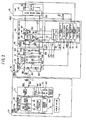
- FIG 2 is a circuit diagram showing an example of a specific configuration of each section of a non-contact power transmission system that includes a power transmitting device and a power receiving device.
- the power transmitting device 10 includes a power transmission control device 20, a power transmitting section 12, and a waveform monitor circuit 14.
- the power transmission control device 20 includes a power-transmitting-side control circuit 22, an oscillation circuit 24, a driver control circuit 26, and a waveform detection circuit 28.
- the power receiving device 40 includes a power receiving section 42, a load modulation section 46, a power supply control section 48, and a power reception control device 50.
- a load 90 includes a charge control device 92 and a battery (secondary battery) 94. The details are given below.
- a power-transmitting-side electronic instrument such as the charger 500 includes at least the power transmitting device 10 shown in FIG. 2 .
- a power-receiving-side electronic instrument such as the portable telephone 510 includes at least the power receiving device 40 and the load 90.
- the configuration shown in FIG 2 implements a non-contact power transmission (contactless power transmission) system that transmits power from the power transmitting device 10 to the power receiving device 40 by electromagnetically coupling the primary coil L1 and the secondary coil L2 to supply power (voltage VOUT) to the load 90 from a voltage output node NB6 of the power receiving device 40.
- a non-contact power transmission contactless power transmission
- the power transmitting device 10 may include the primary coil L1, the power transmitting section 12, the waveform monitor circuit 14, the display section 16, and the power transmission control device 20.
- the power transmitting device 10 and the power transmission control device 20 are not limited to the configuration shown in FIG. 2 . Various modifications may be made such as omitting some (e.g., display section and waveform monitor circuit) of the elements, adding other elements, or changing the connection relationship.
- the power transmitting section 12 generates an alternating-current voltage having a given frequency during power transmission, and generates an alternating-current voltage having a frequency that differs depending on data during data transfer.
- the power transmitting section 12 supplies the alternating-current voltage to the primary coil L1.
- FIGS. 3A and 3B are views illustrative of an example of the principle of information transmission between the power-transmitting-side instrument and the power-receiving-side instrument.
- Information is transmitted from the primary-side instrument to the secondary-side instrument utilizing frequency modulation.
- Information is transmitted from the secondary-side instrument to the primary-side instrument utilizing load modulation.
- the power transmitting device 10 generates an alternating-current voltage having a frequency f1 when transmitting data "1" to the power receiving device 40, and generates an alternating-current voltage having a frequency f2 when transmitting data "0" to the power receiving device 40, for example.
- the power receiving device 40 can switch the load state between a low-load state and a high-load state by load modulation to transmit data "0" or "1" to the primary-side instrument (power transmitting device 10).
- the power transmitting section 12 may include a first power transmitting driver that drives one end of the primary coil L1, a second power transmitting driver that drives the other end of the primary coil L1, and at least one capacitor that forms a resonant circuit with the primary coil L1.
- Each of the first and second power transmitting drivers included in the power transmitting section 12 is an inverter circuit (or buffer circuit) that includes a power MOS transistor, for example, and is controlled by the driver control circuit 26 of the power transmission control device 20.
- the primary coil L1 (power-transmitting-side coil) is electromagnetically coupled to the secondary coil L2 (power-receiving-side coil) to form a power transmission transformer.
- the portable telephone 510 is placed on the charger 500 so that a magnetic flux of the primary coil L1 passes through the secondary coil L2, as shown in FIG 1 .
- the charger 500 and the portable telephone 510 are physically separated so that a magnetic flux of the primary coil L1 does not pass through the secondary coil L2.
- the waveform monitor circuit 14 is a circuit that detects an induced voltage in the primary coil L1.
- the waveform monitor circuit 14 includes resistors RA1 and RA2, and a diode DA1 provided between a connection node NA3 of the resistors RA1 and RA2 and a power supply GND (low-potential-side power supply in a broad sense), for example.
- a signal PHIN obtained by dividing the induced voltage in the primary coil L1 using the resistors RA1 and RA2 is input to the waveform detection circuit 28 of the power transmission control device 20.
- the display section 16 displays the state (e.g., power transmission or ID authentication) of the non-contact power transmission system using a color, an image, or the like.
- the display section 16 is implemented by a light-emitting diode (LED), a liquid crystal display (LCD), or the like.
- the power transmission control device 20 controls the power transmitting device 10.
- the power transmission control device 20 may be implemented by an integrated circuit device (IC) or the like.
- the power transmission control device 20 includes the power-transmitting-side control circuit 22, the oscillation circuit 24, the driver control circuit 26, and the waveform detection circuit 28.
- the power-transmitting-side control circuit 22 controls the power transmitting device 10 and the power transmission control device 20.
- the power-transmitting-side control circuit 22 may be implemented by a gate array, a microcomputer, or the like.
- the power-transmitting-side control circuit 22 performs sequence control and a determination process necessary for power transmission, load detection, frequency modulation, foreign object detection, removal (detachment) detection, and the like.
- the power-transmitting-side control circuit 22 starts temporary power transmission for position detection and ID authentication targeted at the power receiving device 40 when the switch (SW) has been turned ON (described later).
- the oscillation circuit 24 is formed by a crystal oscillation circuit or the like, and generates a primary-side clock signal.
- the driver control circuit 26 generates a control signal at a desired frequency based on the clock signal generated by the oscillation circuit 24, a frequency setting signal output from the control circuit 22, and the like, and outputs the generated control signal to the power transmitting drivers (not shown) of the power transmitting section 12 to control the operations of the power transmitting drivers.
- the waveform detection circuit 28 monitors the waveform of the signal PHIN that corresponds to an induced voltage at one end of the primary coil L1, and performs load detection, foreign object detection, and the like. For example, when the load modulation section 46 of the power receiving device 40 has performed load modulation for transmitting data to the power transmitting device 10, the signal waveform of the induced voltage in the primary coil L1 changes correspondingly.
- the waveform detection circuit 28 can determine whether the data transmitted from the power receiving device 40 is "0" or "1" by determining whether or not the peak voltage has exceeded a threshold voltage by performing a peak-hold process on the signal waveform of the induced voltage, for example.
- the waveform detection method is not limited to the above-described method.
- the waveform detection circuit 28 may determine whether the power-receiving-side load has increased or decreased utilizing a physical quantity other than the peak voltage.
- the power receiving device 40 may include the secondary coil L2, the power receiving section 42, the load modulation section 46, the power supply control section 48, and a power reception control device 50. Note that the power receiving device 40 and the power reception control device 50 are not limited to the configuration shown in FIG. 2 . Various modifications may be made such as omitting some of the elements, adding other elements, or changing the connection relationship.
- the power receiving section 42 converts an alternating-current induced voltage in the secondary coil L2 into a direct-current voltage.
- a rectifier circuit 43 included in the power receiving section 42 converts the alternating-current induced voltage.
- the rectifier circuit 43 includes diodes DB1 to DB4.
- the diode DB1 is provided between a node NB1 at one end of the secondary coil L2 and a node NB3 (direct-current voltage VDC generation node).
- the diode DB2 is provided between the node NB3 and a node NB2 at the other end of the secondary coil L2.
- the diode DB3 is provided between the node NB2 and a node NB4 (VSS).
- the diode DB4 is provided between the nodes NB4 and NB1.
- Resistors RB1 and RB2 of the power receiving section 42 are provided between the nodes NB1 and NB4.
- a signal CCMPI obtained by dividing the voltage between the nodes NB1 and NB4 using the resistors RB1 and RB2 is input to a frequency detection circuit 60 of the power reception control device 50.
- a capacitor CB 1 and resistors RB4 and RB5 of the power receiving section 42 are provided between the node NB3 (direct-current voltage VDC) and the node NB4 (VSS).
- a divided voltage VD4 obtained by dividing the voltage between the nodes NB3 and NB4 using the resistors RB4 and RB5 is input to a power-receiving-side control circuit 52 and a position detection circuit 56 through a signal line LP2.
- the divided voltage VD4 is input to the position detection circuit 56 as a position detection signal input (ADIN).
- the load modulation section 46 performs a load modulation process. Specifically, when the power receiving device 40 transmits the desired data to the power transmitting device 10, the load modulation section 46 variably changes the load of the load modulation section 46 (secondary side) corresponding to the transmission target data to change the signal waveform of the induced voltage in the primary coil L1.
- the load modulation section 46 includes a resistor RB3 and a transistor TB3 (N-type CMOS transistor) provided in series between the nodes NB3 and NB4.
- the transistor TB3 is ON/OFF-controlled based on a control signal P3Q supplied from the power-receiving-side control circuit 52 of the power reception control device 50 through a signal line LP3.
- a transistor TB2 of the power supply control section 48 is turned OFF so that the load 90 is not electrically connected to the power receiving device 40.
- the signal P3Q when reducing the secondary-side load (high impedance) in order to transmit data "0", the signal P3Q is set at the L level so that the transistor TB3 is turned OFF. As a result, the load of the load modulation section 46 becomes almost infinite (no load).
- the signal P3Q when increasing the secondary-side load (low impedance) in order to transmit data "1", the signal P3Q is set at the H level so that the transistor TB3 is turned ON. As a result, the load of the load modulation section 46 is equivalent to the resistor RB3 (high load).
- the power supply control section 48 controls power supply to the load 90.
- a regulator (LDO) 49 regulates the voltage level of the direct-current voltage VDC obtained by conversion by the rectifier circuit 43 to generate a power supply voltage VD5 (e.g., 5 V).
- the power reception control device 50 operates based on the power supply voltage VD5 supplied from the power supply control section 48, for example.
- a switch circuit formed using a PMOS transistor (M1) is provided between the input terminal and the output terminal of the regulator (LDO) 49.
- a path that bypasses the regulator (LDO) 49 is formed by causing the PMOS transistor (M1) (switch circuit) to be turned ON.
- An NMOS transistor (M2) and a pull-up resistor R8 that function as a bypass control circuit are provided to ON/OFF-control the PMOS transistor (M1) (switch circuit).
- the NMOS transistor (M2) is turned ON when a high-level control signal is supplied to the gate of the NMOS transistor (M2) through a signal line LP4. This causes the gate of the PMOS transistor (M1) to be set at a low level so that the PMOS transistor (M1) is turned ON. As a result, a path that bypasses the regulator (LDO) 49 is formed.
- the NMOS transistor (M2) is turned OFF, the gate of the PMOS transistor (M1) is maintained at a high level through the pull-up resistor R8. Therefore, the PMOS transistor (M1) is turned OFF so that the bypass path is not formed.
- the NMOS transistor (M2) is ON/OFF-controlled by the power-receiving-side control circuit 52 included in the power reception control device 50.
- the transistor TB2 (P-type CMOS transistor) is provided between a power supply voltage (VD5) generation node NB5 (output node of the regulator 49) and the node NB6 (voltage output node of the power receiving device 40), and is controlled based on a signal P1Q output from the power-receiving-side control circuit 52 of the power reception control device 50. Specifically, the transistor TB2 is turned ON when normal power transmission is performed after completion (establishment) of ID authentication.
- VD5 power supply voltage
- NB5 output node of the regulator 49
- NB6 voltage output node of the power receiving device 40
- a pull-up resistor RU2 is provided between the power supply voltage generation node NB5 and a node NB8 of the gate of the transistor TB2.
- the power reception control device 50 controls the power receiving device 40.
- the power reception control device 50 may be implemented by an integrated circuit device (IC) or the like.
- the power reception control device 50 may operate based on the power supply voltage VD5 generated based on the induced voltage in the secondary coil L2.
- the power reception control device 50 may include the (power-receiving-side) control circuit 52, the position detection circuit 56, an oscillation circuit 58, the frequency detection circuit 60, a full-charge detection circuit 62, and a recharge monitor circuit 64.
- the power-receiving-side control circuit 52 controls the power receiving device 40 and the power reception control device 50.
- the power-receiving-side control circuit 52 may be implemented by a gate array, a microcomputer, or the like.
- the power-receiving-side control circuit 52 operates based on a constant voltage (VD5) at the output terminal of the series regulator (LDO) 49 as a power supply voltage.
- the power supply voltage (VD5) is supplied to the power-receiving-side control circuit 52 through a power supply line LP1.
- the power-receiving-side control circuit 52 performs sequence control and a determination process necessary for ID authentication, position detection, frequency detection, full-charge detection, recharge determination, load modulation for authentication communication, load modulation for communication that enables detection of foreign object insertion, and the like.
- the position detection circuit 56 monitors the waveform of the signal ADIN that corresponds to the waveform of the induced voltage in the secondary coil L2, and determines whether or not the positional relationship between the primary coil L1 and the secondary coil L2 is appropriate.
- the position detection circuit 56 converts the signal ADIN into a binary value using a comparator, and determines whether or not the positional relationship between the primary coil L 1 and the secondary coil L2 is appropriate.
- the oscillation circuit 58 includes a CR oscillation circuit or the like, and generates a secondary-side clock signal.
- the frequency detection circuit 60 detects the frequency (f1 or f2) of the signal CCMPI, and determines whether the data transmitted from the power transmitting device 10 is "1" or "0".
- the full-charge detection circuit 62 detects whether or not the battery 94 of the load 90 has been fully charged (charge state). Specifically, the full-charge detection circuit 62 detects the full-charge state by detecting whether a light-emitting device (LEDR) used to indicate the charge state is turned ON or OFF, for example. The full-charge detection circuit 62 determines that the battery 94 has been fully charged (charging has been completed) when the light-emitting device (LEDR) has been turned OFF for a given period of time (e.g., five seconds).
- a light-emitting device LEDR
- the load 90 includes the charge control device 92 that controls charging of the battery 94 and the like.
- the charge control device 92 detects a full-charge state based on the ON/OFF state of the light-emitting device (LEDR).
- the charge control device 92 (charge control IC) may be implemented by an integrated circuit device or the like.
- the battery 94 may be provided with the function of the charge control device 92.
- the load 90 is not limited to a secondary battery.
- a given circuit may serve as a load when the circuit operates.
- the recharge monitor circuit 64 determines whether or not recharging is necessary based on the battery voltage VBAT. For example, the recharge monitor circuit 64 determines that recharging is necessary when the battery voltage VBAT has become lower than a threshold voltage.
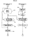
- FIG. 4 is a flowchart showing an outline of an example of the operation of the power transmitting device.
- the power-transmitting-side control circuit 22 of the power transmitting device 10 according to the invention automatically detects installation of the power-receiving-side instrument 510, and manages recharging after full-charging, as described above.
- An operation mode in which the power transmitting device 10 automatically performs a series of operations is referred to as "automatic mode".
- step SA installation detection and a check on the power transmission target
- step SB check on the power transmission environment during normal power transmission
- step SC full-charge detection
- step SD monitoring after full-charging
- step SA When the power transmitting device 10 has been turned ON (step S0), the power transmitting device 10 performs installation detection and a check on the power transmission target (step SA).
- the step SA includes steps S1 to S4.
- the power transmitting device 10 performs intermittent temporary power transmission by automatically and intermittently driving the primary coil L1 in a given cycle (e.g., 0.3 seconds).
- the power transmitting device 10 checks whether or not the power-receiving-side instrument 510 is placed at an appropriate position (step S3), and performs ID authentication on the power-receiving-side instrument 510 (or the power receiving device 40) to determine whether or not the power-receiving-side instrument 510 is an appropriate power transmission target (step S4).
- the power receiving device 40 transmits ID authentication information to the power transmitting device 10 within a given period of time.
- the power receiving device 10 detects installation of the power-receiving-side instrument 510 by checking whether or not the ID authentication information is transmitted from the power receiving device within a given period of time after the intermittent temporary power transmission timing.
- the power transmitting device 10 stops temporary power transmission, and intermittently performs temporary power transmission (initial state).
- the position detection circuit 56 included in the power receiving device 40 shown in FIG 2 checks whether or not the power-receiving-side instrument 510 is placed at an appropriate position (position detection) (step S3) based on a direct-current voltage (ADIN) obtained by rectifying the induced voltage in the secondary coil (L2), for example.
- FIG 12 is a view illustrative of the position detection principle. As shown in FIG 12 , the voltage level of the direct-current voltage ADIN changes corresponding to the positional relationship between the primary coil (L1) and the secondary coil (L2).
- a direct-current voltage (ADIN) at a given level (level V3) cannot be obtained when the power-receiving-side instrument is placed at an inappropriate position (i.e., the power-receiving-side instrument is determined to be placed at an inappropriate position).
- the position detection result may be transmitted from the power receiving device 40 to the power transmitting device 10 utilizing load modulation, for example.
- the power receiving device 40 may notify the power transmitting device 10 that the power-receiving-side instrument is placed at an inappropriate position by not transmitting the ID authentication information to the power transmitting device 10 within a given period of time after receiving temporary power transmission.
- step S4 when the power transmitting device 10 has succeeded in ID authentication (step S4), the power transmitting device 10 starts normal power transmission (step S6).
- the power transmitting device 10 performs metal foreign object detection (step S7) and takeover state detection by means of regular load change detection (steps S8 and S9) during normal power transmission.
- the power transmitting device 10 also detects removal (leave) of the power-receiving-side instrument 510 (step S10).
- step S11 the power transmitting device 10 stops normal power transmission, and returns to the step S1 (automatic intermittent operation).
- a metal foreign object (step S7) and a takeover state (step S10) may be detected based on a change in the waveform of an induced voltage signal of the primary coil (L1). The details are described below.
- FIGS. 13A to 13F are views illustrative of the principle of metal foreign object (conductive foreign object) detection.
- FIGS. 13B to 13F show changes in an induced voltage signal (V(NA2)) of the primary coil L1 shown in FIG 13A corresponding to the relative positions of the primary coil and a metal foreign object (conductive foreign object) MET.
- V(NA2) induced voltage signal
- FIGS. 13B to 13F the waveform (amplitude) of the induced voltage signal V(NA2) when the metal foreign object MET is absent ( FIG. 13F ) differs from the waveform (amplitude) of the induced voltage signal V(NA2) when the metal foreign object (MET) is present ( FIGS. 13B to 13E ).
- the presence or absence of the metal foreign object (MET) can be detected by monitoring the waveform of the induced voltage signal V(NA2) of the primary coil (L1) using the waveform monitor circuit 14 (see FIG. 2 ).
- waveform monitoring includes monitoring the amplitude, monitoring the phases of a current and a voltage, and the like.
- FIGS. 14A to 14D are views illustrative of the principle of removal detection.
- the induced voltage signal V(NA2) of the primary coil (L1) has a waveform shown in FIG. 14B .
- the induced voltage signal V(NA2) of the primary coil (L1) has a waveform shown in FIG 14D .
- the waveform (amplitude) shown in FIG 14D clearly differs from the waveform shown in FIG. 14B . Therefore, whether or not the power-receiving-side instrument has been removed can be detected by monitoring the waveform of the induced voltage signal V(NA2) of the primary coil (L1) using the waveform monitor circuit 14 (see FIG. 2 ).
- Whether or not a takeover state has occurred may be detected (step S9 in FIG. 4 ) by determining whether or not the power-transmitting-side instrument can detect an intermittent (e.g., regular) load modulation signal from the power-receiving-side instrument (described later).
- an intermittent (e.g., regular) load modulation signal from the power-receiving-side instrument (described later).
- step S13 when the power-transmitting-side control circuit 22 of the power transmitting device 10 has detected the full-charge notification (that indicates that the battery has been fully charged) transmitted from the receiving device 40 (step S13), the power-transmitting-side control circuit 22 stops normal power transmission (step S14), and optionally transitions to the monitoring step after full-charging (step SD).
- the full-charge detection circuit 62 included in the power receiving device 40 shown in FIG. 2 detects whether or not the battery 94 has been fully charged.
- the power-receiving-side control circuit 52 included in the power receiving device 40 transmits the full-charge notification to the power transmitting device 10.
- the power-transmitting-side control circuit 22 of the power transmitting device 10 has detected the full-charge notification transmitted from the power receiving device 40, the power-transmitting-side control circuit 22 performs the monitoring step after full-charging (step SD).
- the monitoring step after full-charging includes an intermittent power transmission step in a cycle T10 (step S15), a removal detection step (step S16) (steps S15 and S16 are used to detect removal after full-charging), an intermittent power transmission step in a cycle T20 (step S17), and a recharge request detection step (step S18) (steps S17 and S 18 are used to detect whether or not recharging is necessary). Therefore, the power-transmitting-side control circuit 22 can monitor the load state after the load (battery) 94 of the power-receiving-side instrument 510 has been fully charged to automatically resume recharging.
- the power-transmitting-side control circuit 22 performs intermittent power transmission in an appropriate cycle after a full-charge state has been detected instead of normal power transmission to automatically determine whether or not the load must be recharged, and resumes normal power transmission (step S6) when recharging is necessary. Therefore, the load (battery) 94 is automatically recharged.
- the load (battery) 94 has been necessarily fully charged when the user uses the power-receiving-side instrument 510. This prevents a situation in which the battery becomes charged insufficiently due to discharge. Therefore, convenience to the user can be improved.
- the power-transmitting-side control circuit 22 performs intermittent power transmission for removal detection after full-charging in addition to intermittent power transmission for recharge management (step S15). It may be determined that the power-receiving-side instrument 510 has been removed when no response is transmitted from the power-receiving-side instrument 510 after intermittent power transmission for removal detection has been performed. When the power-transmitting-side control circuit 22 included in the power transmitting device 10 has detected removal of the power-receiving-side instrument 510, the power-transmitting-side control circuit 22 returns to the initial state (i.e., a state in which intermittent temporary power transmission is performed).
- intermittent power transmission for removal detection is performed in the first cycle T10
- intermittent power transmission for recharge management is performed in the second cycle T20.
- the first cycle T10 and the second cycle T20 are provided because it is desirable to optimize the cycle corresponding to the objective.
- the first cycle T10 and the second cycle T20 may be the same.
- the term "full charge” used herein may be broadly interpreted as "a state in which the load of the power receiving device 40 is in a given state", for example. Therefore, the term “load” is not limited to a battery.
- a given circuit of the power-receiving-side instrument 510 may serve as a load.
- a state in which a given circuit that has operated by receiving power from the power transmitting device need not operate corresponds to a state in which the load has been fully charged. Such a case is also included in the technical scope of the aspect of the invention.
- the cycle of intermittent temporary power transmission i.e., the cycle of the automatic intermittent operation in the step S1 shown in FIG. 4
- the cycle of removal detection after full-charging may be longer than the cycle of temporary power transmission. Specifically, unnecessary power consumption increases if removal detection is frequently performed. Therefore, the first cycle T10 of removal detection after full-charging is set at a value (e.g., 5 seconds) longer than the cycle of temporary power transmission to suppress an increase in power consumption.
- the second cycle T20 of full-charge detection is set at a value (e.g., 10 minutes) longer than the first cycle T10. This enables intermittent power transmission to be performed in a cycle corresponding to the objective so that power consumption can be minimized.
- FIG. 5 is a circuit diagram showing an example of the configuration of the power-transmitting-side control circuit.
- the power-transmitting-side control circuit 22 includes a logic circuit 100.
- the logic circuit 100 includes a position detection section 106, an ID authentication section 108, a removal detection section 110, a foreign object detection section 112 (including a takeover state detection section 114), a full-charge notification (power transmission stop request) detection section 116, a recharge request detection section 117, a time-management timer 119, and a power transmission control section 118 that ON/OFF-controls power transmission (temporary power transmission and normal power transmission) based on the detection result of each section.
- the power transmission control section 118 includes an after-full-charge intermittent power transmission control section 121.
- FIG. 6 is a view showing a basic sequence example of the non-contact power transmission system in the automatic mode.
- the user places the power-receiving-side instrument 510 at a predetermined position of the charger 500, for example.
- the power transmitting device 10 performs the automatic intermittent operation to always perform intermittent temporary power transmission (steps S19 and S20).
- the position of the power-receiving-side instrument 510 that has received temporary power transmission is detected (step S21).
- the power transmitting device 10 stops temporary power transmission (step S22).
- the power transmitting device 10 When the power-receiving-side instrument 510 is placed at an appropriate position, the power transmitting device 10 performs ID authentication (step S23). Specifically, the power receiving device 40 transmits the ID authentication information (e.g., manufacturer information, instrument ID number, and rating information) to the power transmitting device 10.
- ID authentication information e.g., manufacturer information, instrument ID number, and rating information
- the power transmitting device 10 starts normal power transmission for the power receiving device 40 (step S26).
- the power transmitting device 10 performs removal detection (step S29), metal foreign object detection (step S30), secondary-side regular load authentication (including an optional secondary-side load reduction process: step S31), and takeover state detection (step S32) during normal power transmission, and stops normal power transmission when one of these states has been detected (step S33).
- the term "load reduction” accompanying secondary-side regular load authentication refers to a process that reduces (or stops) power supplied to the load when performing load modulation to apparently reduce the load state, since the primary-side instrument may not successfully receive a modulation signal when load modulation is performed in a state in which the load state is heavy (described later with reference to FIG. 19 ).
- the power receiving device 40 when the power receiving device 40 has detected a full-charge state, the power receiving device 40 creates the full-charge notification (save frame; power transmission stop request frame), and transmits the full-charge notification to the power transmitting device 10 (step S34).
- the power transmitting device 10 stops normal power transmission, and performs intermittent power transmission after full-charging (step S37).
- the power transmitting device 10 intermittently determines whether or not recharging is necessary (step S38). When the power transmitting device 10 has determined that recharging is necessary, the power transmitting device 10 resumes normal power transmission (step S26).
- the power transmitting device 10 detects whether or not the power-receiving-side instrument 510 has been removed after full-charging (step S39). When the power transmitting device 10 has detected that the power-receiving-side instrument 510 has been removed, the power transmitting device 10 returns to the initial state.
- FIG 7 is a state transition diagram showing the state transition of the non-contact power transmission system that performs the sequence shown in FIG 6 .
- the state of the non-contact power transmission system is roughly divided into an initial state (idle state: ST1), a position detection state (ST2), an ID authentication state (ST3), a power transmission (normal power transmission) state (ST4), a regular load authentication state (ST5) (and a load reduction state (ST6)), and an intermittent power transmission state after full-charging (ST7).
- the non-contact power transmission system transitions from the state ST1 to the state ST2 when installation of the power-receiving-side instrument has been detected by the automatic intermittent operation (Q1), and returns to the state ST1 (Q2) when the position detection result is inappropriate (NG).
- the position detection result is appropriate (OK)
- the non-contact power transmission system transitions to the state ST3.
- ID authentication has been completed successfully (Q6)
- the non-contact power transmission system transitions to the normal power transmission state (ST4).
- the non-contact power transmission system performs removal detection (Q12), metal detection (Q10), takeover state detection (Q17), and full-charge detection (Q14) in the normal power transmission state (ST4).
- the non-contact power transmission system returns to the initial state when one of these states has been detected (Q9, Q11, and Q13).
- the non-contact power transmission system transitions to the intermittent power transmission state ST7 (Q15).
- the non-contact power transmission system performs recharging necessity detection Q18 and removal detection Q16 in the intermittent power transmission state ST7.
- the non-contact power transmission system returns to the initial state (Q20).
- the non-contact power transmission system resumes normal power transmission (Q19).
- the non-contact power transmission system that performs the basic sequence shown in FIGS. 6 and 7 can automatically detect installation of the power-receiving-side instrument (power transmission target). Therefore, the user need not operate a switch and the like. As a result, a convenient non-contact power transmission system is implemented. Since normal power transmission is performed after ID authentication has been completed successfully, power is not transmitted to an inappropriate instrument. Therefore, reliability and safety are improved. Various detection operations (i.e., removal detection, metal foreign object detection, takeover state detection based on secondary-side regular load authentication, and full-charge detection) are performed during normal power transmission, and normal power transmission is promptly stopped and the initial state is recovered when one of these states has been detected. Therefore, unnecessary power transmission does not occur while taking all possible measures against a foreign object.
- detection operations i.e., removal detection, metal foreign object detection, takeover state detection based on secondary-side regular load authentication, and full-charge detection
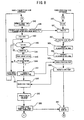
- FIGS. 8 and 9 are flowcharts showing an operation example of the non-contact power transmission system that performs the basic sequence shown in FIG. 6 .
- the left side shows a power-transmitting-side (primary side) operation flow
- the right side shows a power-receiving-side (secondary-side) operation flow.
- the power-transmitting-side control circuit 22 performs the automatic intermittent operation (step S40). Specifically, the power-transmitting-side instrument performs temporary power transmission at given time intervals (e.g., the transmission frequency is f1; step S41), and a timer starts a count operation (step S42).
- the power-transmitting-side instrument performs temporary power transmission at given time intervals (e.g., the transmission frequency is f1; step S41), and a timer starts a count operation (step S42).
- the power-receiving-side instrument transitions from a standby state (step S60) to a power-ON state (step S61) when the power-receiving-side instrument has received temporary power transmission, and determines the position level (position detection).
- position detection determines the position level (position detection).
- the position level is inappropriate (NG)
- the power-receiving-side instrument returns to the initial state (step S60).
- the position level is appropriate (OK)
- the power-receiving-side instrument generates the ID authentication frame (S63), and transmits the ID authentication frame (step S64).
- the power-transmitting-side instrument receives the ID authentication frame (step S44), and determines whether or not a timeout has occurred (step S43). When the power-transmitting-side instrument cannot receive the ID authentication frame within a given period of time, the power-transmitting-side instrument stops temporary power transmission (step S51), and returns to the initial state.
- the power-transmitting-side instrument When the power-transmitting-side instrument has received the ID authentication frame within a given period of time, the power-transmitting-side instrument performs a frame authentication process (step S45). When authentication has succeeded (OK), the power-transmitting-side instrument transmits a permission frame to the power-receiving-side instrument (step S47). When authentication has failed (NG), the power-transmitting-side instrument stops temporary power transmission (step S51), and returns to the initial state.
- the power receiving device 40 checks the permission frame transmitted from the power transmitting device 10 (step S65), and transmits a start frame to the power transmitting device 10 (step S66).
- the power transmitting device 10 checks the start frame (step S48), enables regular load change detection (takeover state detection) (step S49), and starts normal power transmission (step S50).
- the power receiving device 40 receives normal power transmission, and starts charging the load (e.g., battery) (step S67).
- FIG 9 shows the subsequent flow.
- the power transmitting device 10 waits for the full-charge notification (power transmission stop request) from the power receiving device 40 (step S71) while performing removal detection, metal foreign object detection, and takeover state detection (step S70).
- the power receiving device 40 performs regular load modulation for takeover detection while charging the load (step S80), and detects whether or not the load has been fully charged (step S81). Specifically, the full-charge detection circuit 62 determines that the load has been fully charged when the light-emitting diode LEDR has been turned OFF for a given period of time (e.g., 5 seconds). When the power receiving device 40 has detected that the load has been fully charged, the power receiving device 40 transmits the full-charge notification frame (save frame; power transmission stop request) to the power transmitting device 10 (step S82).
- the full-charge notification frame asave frame; power transmission stop request
- the power transmitting device 10 When the power transmitting device 10 has received the full-charge notification frame (save frame; power transmission stop request) from the power receiving device 40, the power transmitting device 10 disables regular load change detection (step S72), and stops power transmission (step S73).
- the takeover state is considered to be a special form of foreign object insertion.
- the takeover state refers to a state in which the power-transmitting-side instrument continuously performs normal power transmission while erroneously regarding a foreign object as the power-receiving-side instrument. For example, when a thin metal sheet has been inserted between the primary coil and the secondary coil to block the primary coil and the secondary coil, since a considerable load is always present with respect to the power-transmitting-side instrument, it is difficult to detect removal of the power-receiving-side instrument, for example.
- a large foreign object may be inserted between the primary coil L1 and the secondary coil L2 after the power receiving device (or the power-receiving-side instrument) has been authenticated and normal power transmission has started.
- a metal foreign object can be detected by monitoring the induced voltage in the primary coil (L1), as described with reference to FIG. 13 .
- the power transmitting device 10 regards the metal foreign object as the load (power-receiving-side instrument). Therefore, removal of the power-receiving-side instrument may not be detected based on the induced voltage in the primary coil L1, as described with reference to FIG. 14 , for example. In this case, power transmission from the power transmitting device 10 is continuously performed although the power-receiving-side instrument is absent so that the temperature of the metal foreign object increases to a large extent.
- a metal foreign object e.g., thin metal sheet
- takeover phenomenon
- FIGS. 15A and 15B are cross-sectional views showing electronic instruments that form a non-contact power transmission system which are illustrative of insertion of a foreign object (takeover state) after normal power transmission has started.
- the portable telephone 510 (electronic instrument including the power receiving device 40) is placed at a predetermined position on the cradle 500 (electronic instrument including the power transmitting device 10).
- Non-contact power transmission is performed from the cradle 500 (charger) to the portable telephone 510 through the primary coil L1 and the secondary coil L2 so that the secondary battery (e.g., battery pack) 94 provided in the portable telephone 510 is charged.
- the secondary battery e.g., battery pack
- a thin sheet-shaped metal foreign object (conductive foreign object) AR is intentionally inserted between the cradle 500 (charger) and the portable telephone 510 during normal power transmission.
- the foreign object AR When the foreign object AR has been inserted, power supplied from the primary-side instrument (cradle 500) to the secondary-side instrument (portable telephone terminal 510) is almost entirely consumed by the foreign object (AR) (i.e., the transmitted power is taken over), whereby the foreign object AR is likely to generate heat. Therefore, when the state shown in FIG. 15B has occurred, the power transmitting device 10 included in the primary-side instrument (cradle 500) must detect insertion of the foreign object AR and immediately stop normal power transmission.
- the amplitude of the voltage induced in the primary coil L1 increases as the load of the power receiving device increases, and the amplitude of the voltage induced in the primary coil L1 decreases as the load of the power receiving device decreases. If the secondary battery 94 of the portable telephone 510 is normally charged, the load of the power receiving device 40 gradually decreases with the passage of time. When the load of the power receiving device 40 has rapidly increased, the power transmitting device 10 can detect the rapid increase in load since the power transmitting device 10 monitors a change in the load of the power receiving device 40.
- the power transmitting device 10 cannot determine whether the increase in load has occurred due to the load (secondary battery 94 of portable telephone terminal), mispositioning between the portable telephone terminal 510 and the cradle 500, or insertion of a foreign object. Therefore, insertion of a foreign object cannot be detected using the method in which the power transmitting device 10 merely detects a change in the load of the power receiving device 40.
- the power receiving device 40 intermittently changes the load of the power receiving device 40 during normal power transmission while supplying power to the load (e.g., secondary battery) (regular load modulation operation) to transmit information to the power transmitting device 10.
- the load e.g., secondary battery
- the following items are confirmed when the power transmitting device 10 has detected the information due to an intermittent change in load at a given timing.
- the power transmitting device 10 cannot detect an intermittent (e.g., regular) change in the load of the power receiving device. It is most likely that an intermittent change in load cannot be detected after the above-mentioned items (1) to (3) have been confirmed because the foreign object AR has been inserted (item (3)). Specifically, the power transmitting device 10 can determine that the power transmitting device 10 has become unable to detect an intermittent change in load due to insertion of the foreign object AR.
- an intermittent e.g., regular
- FIGS. 16A and 16B are views illustrative of a specific embodiment when intermittently changing the load of the power receiving device so that insertion of a foreign object can be detected.
- an intermittent change in the load of the power receiving device is indicated by a change in secondary current (current that flows through the secondary coil L2).
- the load of the power receiving device intermittently changes at times t1, t2, t3, t4, t5, ...
- the load changes in a cycle T3.
- the load decreases in a period T2 starting from the time t1, and increases in the subsequent period T1, for example.
- Such a cyclic change in load is repeated in the cycle T3.
- FIG. 16B shows a change in primary coil voltage (induced voltage at one end of the primary coil) with respect to a change in secondary load current.
- the secondary-side load is heavy in the period T1, and is light in the period T2, as described above.
- the amplitude (peak value) of the induced voltage (primary coil voltage) at one end of the primary coil (L1) changes corresponding to the change in secondary-side load. Specifically, the amplitude increases in the period T1 in which the load is heavy, and decreases in the period T2 in which the load is light. Therefore, the power transmitting device 10 can detect a change in the load of the power receiving device 40 by detecting the peak of the primary coil voltage using the waveform detection circuit 28 (see FIG. 2 ), for example.
- the load change detection method is not limited to the above-described method.
- the phase of the primary coil voltage or the phase of the primary coil current may be detected.
- the load can be easily modulated by switching the transistor, for example.
- the peak voltage of the primary coil or the like can be accurately detected using an analog or digital basic circuit. Therefore, the above method does not impose load on the instrument to a large extent while facilitating implementation.
- the above-described method is also advantageous in terms of a reduction in mounting area and cost.
- insertion of a foreign object can be easily and accurately detected without adding a special configuration by employing a novel method in which the power receiving device 40 transmits information obtained by intermittently (and cyclically) changing the load during normal power transmission and the power transmitting device 10 detects the change in load.
- FIG. 17 is a circuit diagram showing the main configuration of the non-contact power transmission system shown in FIG. 2 relating to detection of foreign object insertion (takeover state).
- the same sections as in FIG 2 are indicated by the same reference symbols.
- a bold line indicates a portion that plays an important role in detecting foreign object insertion.
- a notable circuit configuration of the power receiving device 40 shown in FIG 17 includes the load modulation transistor TB3 of the load modulation section 46 (see FIG. 2 ), the power supply control transistor TB2 of the power supply control section 48 (see FIG 2 ), and the power-receiving-side control circuit 52 that ON/OFF-controls these transistors (TB2 and TB3). It is also important that the voltages at the input terminal and the output terminal of the series regulator (LDO) 49 are input to the power-receiving-side control circuit 52 through the signal lines LP2 and LP1 so that the load state (degree of load) of the battery 94 (secondary battery) included in the load 90 can be detected by monitoring the voltage across the series regulator (LDO) 49.
- LDO series regulator
- the configuration of the power transmission control device 20 of the power transmitting device 10 is also important. Specifically, it is important that the peak value (amplitude) of the induced voltage in the primary coil (L1) is detected by the waveform detection circuit 28 and a change in the load of the power receiving device 40 is detected by the power-transmitting-side control circuit 22.
- the power receiving device 40 modulates the load during normal power transmission (continuous power transmission after authentication), and transmits a foreign object detection pattern PT1 to the power transmitting device 10.
- the power-transmitting-side control circuit 22 of the power transmitting device 10 (successively or intermittently) monitors a change in the load of the power receiving device 40 during normal power transmission.
- the power-transmitting-side control circuit 22 determines that the foreign object AR has been inserted when the power-transmitting-side control circuit 22 has become unable to receive the foreign object detection pattern PT1, and stops normal power transmission.
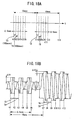
- FIGS. 18A and 18B are views illustrative of a specific preferred embodiment of load modulation that enables foreign object detection.
- FIG. 18A is a view showing a load modulation timing example
- FIG 18B is a view showing a change in the load of the power receiving device detected by the power transmitting device in detail.
- load modulation that enables foreign object detection is cyclically (regularly) performed in a cycle of 5 seconds (10 seconds), for example.
- Load modulation that enables foreign object detection is performed in a period from a time t1 to a time t6 and a period from a time t7 to a time t12.
- the period from the time t1 to the time t6 (from the time t7 to the time t12) is 0.5 seconds.
- the degree of load is changed in units of 0.1 seconds (100 msec) obtained by equally dividing 0.5 seconds by five.
- a bold bidirectional line indicates a period in which the load is heavy. Specifically, the load increases in a period from the time t1 to the time t2, a period from the time t3 to the time t4, a period from the time t5 to the time t6, a period from the time t7 to the time t8, a period from the time t9 to the time t10, and a period from the time t11 to the time t12.
- a period in which the load increases is referred to as a period TA.
- the load decreases in a period from the time t2 to the time t3, a period from the time t4 to the time t5, a period from the time t8 to the time t9, and a period from the time t10 to the time t11.
- a period in which the load decreases is referred to as a period TB.
- the load of the power receiving device is intermittently changed cyclically (i.e., in cycle units (in units of one cycle)) during normal power transmission, and the load is intermittently changed a plurality of times at given intervals within one cycle.
- the power transmitting device 10 and the power receiving device 40 can transfer the information relating to a change in load in synchronization by cyclically changing the load (i.e., the power transmitting device 10 can easily determine the timing at which the load of the power receiving device 40 changes).
- the load is intermittently changed a plurality of times at given intervals only in a given period (from the time t1 to the time t6) within one cycle (e.g., from the time t1 to the time t7).
- the load is modulated only in the first period (0.5 seconds) of one cycle (10 seconds). The reasons that the load is modulated in this manner are as follows.
- load modulation since a change in load (load modulation) during normal power transmission may affect power supply to the load (battery 94 shown in FIG 17 ), it is undesirable to frequently change the load to a large extent. Therefore, one cycle of load modulation is increased to some extent (a foreign object can be detected even if the cycle of load modulation is increased to some extent).
- the load is intermittently changed a plurality of times at given intervals only in a given period within one cycle.
- the power transmitting device may not appropriately detect an intermittent change in the load of the power receiving device due to a change in the load state of the load with the passage of time or a change in surrounding conditions. Therefore, one cycle is increased (10 seconds in FIG 18A ), and the load is intermittently modulated a plurality of times (five times in FIG 18A ) only in a short period (0.5 seconds in FIG 18A ) within one cycle, for example.
- the power transmitting device 10 can detect a foreign object (AR) with high accuracy while minimizing an effect on power supply to the load (battery 94) (e.g., charging a battery pack) by performing load modulation in this manner.
- a foreign object AR
- the load battery 94
- FIG 18B shows an example of a change in the amplitude of the induced voltage at one end of the primary coil (L1) of the power transmitting device 10 corresponding to the load of the power receiving device.
- the load state of the load (battery 94) differs between a load modulation period (t1 to t6) in the first cycle and a load modulation period (t7 to t12) in the second cycle.
- the load state of the load (battery 94) increases in the second cycle so that the peak value of the primary coil voltage increases.
- the difference between the primary coil voltage in the period TA in which the load increases and the primary coil voltage in the period TB in which the load decreases is ⁇ V1.
- the power-transmitting-side control circuit 22 of the power transmitting device 10 can detect a change in the load of the power receiving device 40 from the difference ⁇ V1 in the amplitude of the primary coil voltage.
- the ratio of a modulation current (Imod) due to load modulation to the charging current (Iload) decreases so that the difference in primary coil voltage caused by turning the modulation current (Imod) ON/OFF decreases to ⁇ V2 ( ⁇ V2 ⁇ V1).
- the modulation current (Imod) is buried in the charging current (Iload) supplied to the load (battery 94). Therefore, when the load (battery 94) is heavy, it is difficult for the power transmitting device 10 to detect a change in load as compared with the case where the load is light.
- the load state of the load (battery 94) is compulsorily reduced by reducing the amount of power supplied to the load (battery 94) so that the primary-side device can easily detect a change in load due to load modulation.
- the load reduction measures are described below.
- the relative ratio of the ON/OFF current (Imod) due to load modulation increases when the amount of current supplied to the load 94 is small (when the load is light), so that the power transmitting device 10 can easily detect a change in load due to the ON/OFF operation.
- the power receiving device 40 monitors the load state of the load 94 during normal power transmission, and the amount of power supplied to the load 94 is compulsorily reduced based on the above consideration when the load 94 is heavy (i.e., a large amount of current is supplied to the load 94) when the power receiving device 40 performs load modulation that enables foreign object detection.
- the amount of power supplied to the load 94 may be reduced by temporarily (or intermittently) stopping power supply.
- the power transmitting device 10 can easily detect the signal due to load modulation. Therefore, the foreign object detection accuracy is maintained at a desired level even when the load 94 is heavy. Since at least a minimum amount of power is always supplied to the load 94 even when compulsorily reducing the load 94, a problem in which the electronic circuit (charge control device 92) of the load 94 cannot operate does not occur.
- load modulation that enables detection of foreign object insertion is intermittently performed at appropriate intervals taking the effect on power supply to the load 94 into consideration, power supply to the load 94 is not adversely affected even if the load is compulsorily reduced. For example, a problem in which the charging time of the battery pack increases to a large extent does not occur.
- the load change detection accuracy of the power transmitting device 10 can be maintained at a desired level even if the load 94 is heavy by causing the power receiving device 40 to monitor the state of the load 94 and compulsorily reduce the load state of the load 94, as required, when performing load modulation which enables detection of insertion of a foreign object.
- FIGS. 19A to 19E are views illustrative of the load reduction operation.
- FIG 19A is a view showing a state in which the load state of the load is light.
- FIG. 19B is a view showing a state in which the load state of the load is heavy.
- FIG 19C is a view showing a change in primary coil voltage in the state shown in FIG 19B.
- FIG. 19D is a view showing a state in which the load is reduced by causing the power supply control transistor to be turned ON/OFF or setting the power supply control transistor in a half ON state.
- FIG 19E is a view showing a change in primary coil voltage in the state shown in FIG 19D .
- the power transmitting device 10 can sufficiently detect a change in load due to load modulation without causing the power receiving device 40 to perform the operation of reducing the load. Therefore, the power supply control transistor TB2 is always turned ON.
- the load modulation transistor TB3 is intermittently turned ON/OFF to implement load modulation.
- the power receiving device 40 performs the operation that reduces the load when performing load modulation.
- the power receiving device 40 causes the power supply control transistor TB2 to be successively turned ON/OFF, or sets the power supply control transistor TB2 in a half ON state.
- the amount of power supplied to the load 94 can be compulsorily reduced (power supply may be temporarily stopped) using a digital method which causes the power receiving device 40 to successively turn the power supply control transistor TB2 provided in a power supply path ON/OFF to intermittently supply power to the load 94.
- An operation of successively switching a transistor is generally employed for a digital circuit, and is easily implemented. Moreover, it is possible to accurately reduce the amount of power supplied to the load by selecting the switching frequency.
- the amount of power supplied to the load 94 can also be reduced using an analog method in which an intermediate voltage between a complete ON voltage and a complete OFF voltage is supplied to the gate of the power supply control transistor (PMOS transistor) to set the PMOS transistor in a half ON state.
- This method has an advantage in that the on-resistance of the power supply control transistor (PMOS transistor) can be finely adjusted by controlling the gate voltage.
- the amplitude of the primary coil voltage in a state in which the load is heavy changes from V10 to V20 by compulsorily reducing the load.
- "X" indicates the amount by which the load 94 is compulsorily reduced.
- the difference in amplitude of the primary coil voltage increases from ⁇ V2 (see FIG. 19C ) to ⁇ V3 ( ⁇ V3> ⁇ V2) by compulsorily reducing the load 94, whereby the power transmitting device 10 can easily detect a change in the load of the power receiving device 40 due to load modulation.
- the power transmitting device can reliably detect a change in load even when the load is heavy by causing the power receiving device to reduce the load (including temporarily stopping the load current) while performing load modulation.
- the regular load change detection section 14 (see FIG. 5 ) of the power-transmitting-side control circuit 22 included in the power transmission control device 20 determines that a foreign object (AR) has been inserted between the primary coil (L1) and the secondary coil (L2) when the regular load change detection section 14 cannot detect an intermittent change in the load of the power receiving device 40 during normal power transmission, and stops power transmission. This reliably prevents heat generation from the foreign object (AR), a skin burn, and damage to and destruction of the instrument. Therefore, highly reliable foreign object insertion measures are implemented for a non-contact power transmission system.
- the power-transmitting-side control circuit 22 detect a change in load in cycle units and determine that a foreign object has been inserted between the primary coil and the secondary coil when the power-transmitting-side control circuit 22 cannot detect a change in load over a given number of cycles.
- the power-transmitting-side control circuit 22 detects a change in the load of the power receiving device in cycle units, and stops normal power transmission when the power-transmitting-side control circuit 22 cannot detect a change in load over a given number of cycles (e.g., three cycles). This increases the foreign object insertion detection accuracy, thereby preventing a situation in which the power-transmitting-side control circuit 22 erroneously stops normal power transmission when a change in load cannot be detected due to an accidental factor.
- a change in the load of the power receiving device 40 can be detected by detecting the waveform of the induced voltage in the primary coil (L1).
- the waveform can be detected by the waveform detection circuit 22.
- the load change detection method is not limited to the above-described method.
- a change in load may be detected by detecting the phase of the induced voltage or current in the primary coil.
- a novel power receiving device 10 having a function of detecting foreign object insertion (takeover) by regular load authentication is implemented. According to this embodiment, insertion of a foreign object between the primary coil and the secondary coil can be accurately detected by simple signal processing while reducing the number of parts to implement highly reliable safety measures relating to non-contact power transmission.
- the power transmission stop function due to regular load authentication can be utilized to compulsorily stop inappropriate power transmission in addition to detect the takeover state. For example, power transmission from the power-transmitting-side instrument is reliably stopped even when removal of the power-receiving-side instrument has not been detected for some reason or the power-receiving-side instrument cannot perform regular load modulation due to breakage or failure. Therefore, the safety and the reliability of the non-contact power transmission system are remarkably improved by providing the regular load authentication function.
- This embodiment illustrates recharging after full-charging.
- the portable telephone power-receiving-side instrument
- the charger cradle
- the power transmitting device can automatically detect necessity of recharging after full-charging.
- FIGS. 10A and 10B are sequence diagrams showing a series of processes of the non-contact power transmission system that manages recharging after full-charging. The process shown in FIG. 10B is performed after the process shown in FIG. 10A .
- the non-contact power transmission system transitions to a post-full-charge standby mode when the battery 94 (see FIG. 2 ) has been fully charged.
- the power transmitting device 10 intermittently transmits power to the power receiving device 40 while notifying the power receiving device 40 that the power transmitting device 10 is set in the post-full-charge standby mode.
- the power receiving device 40 checks the battery voltage VBAT.
- the power receiving device 40 determines that the battery 94 requires recharging, and transmits a recharge command to the power transmitting device 10. Therefore, the power transmitting device 10 resumes normal power transmission to the power receiving device 40. As a result, the battery 94 is recharged. The post-full-charge standby mode is canceled at this time. When the battery voltage VBAT is higher than the recharge voltage, the post-full-charge standby mode is maintained. The details are described below.
- the power-transmitting-side control circuit 22 shown in FIG. 2 stops normal power transmission to the power receiving device 40 and performs intermittent power transmission.
- the power-transmitting-side control circuit 22 resumes normal power transmission to the power receiving device 40.
- the power-receiving-side control circuit 52 shown in FIG. 2 transmits a recharge command that indicates information relating to the recharge state of the battery 94 to the power transmitting device 10 in the intermittent power transmission period.
- the full-charge state of the battery 94 is detected by the full-charge detection circuit 62, and the recharge state of the battery 94 is monitored by the recharge monitor circuit 64.
- the term "information relating to the recharge state” refers to information used to determine whether or not the battery 94 requires recharging, and includes information relating to whether or not the battery 94 requires recharging and information relating to the battery voltage VBAT after the battery 94 has been fully charged.
- the power-receiving-side control circuit 52 transmits a full-charge command (full-charge information) which indicates that the battery 94 has been fully charged to the power transmitting device 10 by means of load modulation performed by the load modulation section 46, for example.
- the control circuit 52 stops outputting (supplying) the voltage VOUT to the charge control device 92.
- the control circuit 52 determines that the battery 94 has been fully charged (charging has been completed) when the full-charge detection circuit 62 has detected that the light-emitting device LEDR used to display the charge state has been turned OFF for 5 seconds, for example.
- the control circuit 52 then generates a frame for transmitting the full-charge command, and transmits the generated frame to the power transmitting device 10 by means of load modulation by controlling a signal P3Q.
- the control circuit 22 When the power-transmitting-side control circuit 22 has received the full-charge command during normal power transmission to the power receiving device 40, the control circuit 22 sets a full-charge flag FC to "1", as indicated by A3 in FIG 10A , and stops power transmission to the power receiving device 40 for the first period T1 (e.g., 1 second), as indicated by A4. The control circuit 22 then resumes power transmission (intermittent power transmission), as indicated by A5.
- the control circuit 22 transmits a recharge detection command which instructs the power receiving device 40 to perform detection of the recharge state of the battery 94 (detection of whether or not the battery 94 requires recharging or detection of the battery voltage after the battery 94 has been fully charged) in the intermittent power transmission period after resuming power transmission, as indicated by A6.
- the power transmitting device 10 generates a frame of the recharge detection command using the method described with reference to FIG 3A , and transmits the generated frame to the power receiving device 40.
- the control circuit 22 determines that a timeout has occurred, as indicated by A7.
- the control circuit 22 again stops power transmission to the power receiving device 40 for the period T1, as indicated by A8, and again transmits the recharge detection command to the power receiving device 40 in the intermittent power transmission period after resuming power transmission, as indicated by A9.
- the power transmission suspension period T1 may be referred to as a first period
- the timeout wait period T2 may be referred to as a second period.
- the power reception control device 50 when power transmission from the power transmitting device 10 has been stopped after the power reception control device 50 has transmitted the full-charge command, the power reception control device 50 is reset. Specifically, the power supply voltage becomes 0 V since power is not supplied from the power transmitting device 10 so that the power reception control device 50 is reset.
- the power-receiving-side control circuit 52 monitors the recharge state of the battery 94, as indicated by A12.
- the power-receiving-side control circuit 52 monitors and determines whether or not the battery 94 requires recharging. Alternatively, the power-receiving-side control circuit 52 may monitor the battery voltage VBAT and transmit information relating to the battery voltage VBAT to the power transmitting device 10. The power-receiving-side control circuit 52 monitors the recharge state of the battery 94 based on the monitoring result of the recharge monitor circuit 64 shown in FIG 2 .
- the power-receiving-side control circuit 52 transmits the recharge command which indicates information relating to the recharge state of the battery 94 to the power transmitting device 10. For example, when the power-receiving-side control circuit 52 has determined that the battery 94 requires recharging based on the monitoring result of the recharge monitor circuit 64, the power-receiving-side control circuit 52 transmits the recharge command to the power transmitting device 10. When the power-transmitting-side control circuit 22 has received the recharge command from the power receiving device 40, the power-transmitting-side control circuit 22 resets the full-charge flag FC to "0", as indicated by B2, and resumes normal power transmission to the power receiving device 40, as indicated by B3.
- the power-transmitting-side control circuit 22 resumes normal power transmission when the power-transmitting-side control circuit 22 has determined that the battery 94 requires recharging based on the recharge command. As a result, the battery 94 starts to be recharged so that the battery 94 of which the voltage has decreased can be recharged.
- FIG. 11 shows a summary of the process of the non-contact power transmission system that automatically performs ID authentication, normal power transmission, full-charge detection, and recharge management.
- FIG 11 is a flowchart showing the process of the non-contact power transmission system that automatically performs ID authentication, normal power transmission, full-charge detection, and recharge management.
- the power-transmitting-side process is as follows.
- the power-transmitting-side instrument primary-side instrument
- the power-transmitting-side instrument resets the full-charge flag FC to "0" (steps S1 and S2).
- the power-transmitting-side instrument then starts normal power transmission to the power-receiving-side instrument (step S3).
- the power-transmitting-side instrument then performs removal (leave) detection (step S4).
- the power-transmitting-side instrument has detected removal (leave) of the power-receiving-side instrument, the power-transmitting-side instrument transitions to the normal standby mode.
- the power-transmitting-side instrument detects removal when the portable telephone 510 has been physically separated from the charger 500 in FIG. 1A so that a magnetic flux of the primary coil L1 does not pass through the secondary coil L2, and then transitions to the normal standby mode.
- the power-transmitting-side instrument does not perform intermittent power transmission, differing from the post-full-charge standby mode.
- the power-transmitting-side instrument completely stops power transmission until the portable telephone 510 is again placed on the charger 500.
- the power-transmitting-side instrument determines whether or not the full-charge command has been received from the power-receiving-side instrument (step S5). When the power-transmitting-side instrument has determined that the full-charge command has not been received from the power-receiving-side instrument, the power-transmitting-side instrument returns to the step S4. When the power-transmitting-side instrument has determined that the full-charge command has been received from the power-receiving-side instrument, the power-transmitting-side instrument sets the full-charge flag FC to "1" (step S6). The power-transmitting-side instrument then stops power transmission to the power-receiving-side instrument during the first period (power transmission suspension period) T1 (step S7). The period T1 is measured by a count process based on a power-transmitting-side clock signal.
- the power-transmitting-side instrument resumes power transmission (intermittent power transmission), and transmits the recharge detection command to the power-receiving-side instrument (step S8). Specifically, the power-transmitting-side instrument generates a frame that instructs detection of the recharge state, and transmits the generated frame to the power-receiving-side instrument by frequency modulation. The power-transmitting-side instrument then waits for expiration of the second period (timeout wait period) T2 (i.e., waits for a timeout to occur) (step S9).
- timeout wait period T2
- the power-transmitting-side instrument waits for the power-receiving-side instrument to operate upon cancellation of the reset state due to intermittent power transmission and transmit the recharge command.
- the power-transmitting-side instrument performs removal detection until the second period T2 expires (step S10).
- the power-transmitting-side instrument transitions to the normal standby mode.
- the power-transmitting-side instrument monitors whether or not the recharge command has been received from the power-receiving-side instrument until the second period T2 expires (step S11).
- the power-transmitting-side instrument returns to the step S9.
- the power-transmitting-side instrument When the second period T2 has elapsed (i.e., timeout has occurred), the power-transmitting-side instrument returns to the step S7, and again stops power transmission to the power-receiving-side instrument.
- the power-transmitting-side instrument performs intermittent power transmission after the power transmission suspension period T1 has expired, and again transmits the recharge detection command to the power-receiving-side instrument (step S8). As described above, the power-transmitting-side instrument repeatedly stops power transmission and performs intermittent power transmission until the power-transmitting-side instrument receives the recharge command from the power-receiving-side instrument.
- the power-transmitting-side instrument When the power-transmitting-side instrument has received the recharge command from the power-receiving-side instrument in the step S11, the power-transmitting-side instrument returns to the step S2, and resets the full-charge flag FC to "0". The power-transmitting-side instrument the resumes normal power transmission for recharging the battery 94 (step S3). As a result, the battery 94 of which the voltage has decreased starts to be recharged.
- the power-receiving-side process is as follows.
- the power-receiving-side instrument starts normal power receiving (steps S21 and S22).
- the power-receiving-side instrument determines whether or not the battery 94 has been fully charged.
- the power-receiving-side instrument transmits the full-charge command to the power-transmitting-side instrument (steps S23 and S24).
- the power-receiving-side instrument generates a frame which indicates that the battery 94 has been fully charged, and transmits the generated frame to the power-transmitting-side instrument by load modulation.
- the power-transmitting-side instrument sets the full-charge flag FC to "1", and stops power transmission (steps S6 and S7).
- the power-receiving-side instrument stops outputting the voltage VOUT to the charge control device 92 (step S25).
- the power-receiving-side instrument causes the transistors TB2 and TB1 shown in FIG. 2 to be turned OFF to electrically disconnect the load 90.
- the control circuit 52 causes the transistor TB2 to be turned OFF by setting the signal P1Q at the H level.
- the power-receiving-side instrument When the power-transmitting-side instrument has stopped power transmission in the step S7 in FIG 11 , the power-receiving-side instrument is reset since power is not supplied to the power-receiving-side instrument. When the power-transmitting-side instrument has then started intermittent power transmission, power is supplied to the power-receiving-side instrument. Therefore, the power-receiving-side power supply voltage rises, whereby the reset state is canceled (step S26). The power-receiving-side instrument then determines whether or not the recharge detection command has been received (step S27). When the power-receiving-side instrument has not received the recharge detection command, the power-receiving-side instrument transitions to a normal ID authentication process. Specifically, a normal standby mode process is performed.
- the power-receiving-side instrument determines whether or not the battery 94 requires recharging (step S28). Specifically, the power-receiving-side instrument determines whether or not the battery voltage VBAT is lower than the recharge voltage (e.g., 3.9 V). When the power-receiving-side instrument has determined that the battery 94 does not require recharging, the power-receiving-side instrument does not respond to the power-transmitting-side instrument. Therefore, the power-transmitting-side instrument determines that a timeout has occurred in the step S9, and stops power transmission so that the power-receiving-side instrument is reset.
- the battery voltage VBAT e.g., 3.9 V
- the power-receiving-side instrument When the power-receiving-side instrument has determined that the battery 94 requires recharging in the step S28, the power-receiving-side instrument transmits the recharge command (step S29). When the power-transmitting-side instrument has received the recharge command, the power-transmitting-side instrument resets the full-charge flag FC to "0" and resumes normal power transmission (steps S2 and S3). The power-receiving-side instrument also resumes normal power receiving (step S22) so that the post-full-charge standby mode is canceled.
- the power-transmitting-side instrument stops power transmission (step S7).
- the power-receiving-side instrument stops outputting the voltage VOUT to the charge control device 92 (step S25), and transitions to the post-full-charge standby mode.
- the power reception control device 50 is reset.
- the charge control device 92 is also reset. Therefore, a standby current that flows through the power reception control device 50 and the charge control device 92 can be significantly reduced so that power consumption can be reduced.
- the power-transmitting-side instrument performs intermittent power transmission and transmits the recharge detection command (step S8).
- the power-receiving-side instrument monitors the recharge state based on the received recharge detection command when the reset state has been canceled (steps S27 and S28).
- the power-receiving-side instrument transmits the recharge command (step S29).
- the power-transmitting-side instrument transmits the recharge detection command to the power-receiving-side instrument in the intermittent power transmission period after power transmission has been stopped.
- the power-receiving-side instrument released from the reset state can start monitoring the recharge state based on the recharge detection command from the power-transmitting-side instrument as a trigger, even if the power-receiving-side instrument does not store the information relating to the full-charge state or the recharge state.
- the power-receiving-side instrument can notify the power-transmitting-side instrument that recharging is necessary by transmitting the recharge command. This makes it possible to appropriately recharge the battery 94 after the battery 94 has been fully charged.
- the power-transmitting-side instrument When the power-transmitting-side instrument has not received the recharge command within the period T2 so that a timeout has occurred, the power-transmitting-side instrument stops power transmission (steps S9 and S7). Specifically, the power-transmitting-side instrument repeatedly stops power transmission and performs intermittent power transmission until the power-transmitting-side instrument receives the recharge command. Therefore, it suffices that the power-receiving-side instrument operate only in the intermittent power transmission period.
- the standby current in the post-full-charge standby mode can be significantly reduced by sufficiently increasing the power transmission suspension period T1. Therefore, the battery 94 can be optimally recharged while minimizing unnecessary power consumption.
- This embodiment illustrates detection of removal (leave) of the power-receiving-side instrument (secondary-side instrument) after full-charging. Whether or not the power-receiving-side instrument has been removed after full-charging may be detected by causing the power transmitting device 10 to perform intermittent power transmission to the power receiving device 40, and determining whether or not the power transmitting device 10 can detect the ID authentication information from the power receiving device 40, for example. Specifically, normal power transmission is stopped when the battery 94 has been fully charged. Therefore, the charge control device 92 (see FIG. 2 ) provided in the load 90 is reset and returns to the initial state.
- the power transmitting device 10 When the power transmitting device 10 has performed intermittent power transmission at given intervals after the battery has been fully charged, the power receiving device 40 that has received power by intermittent power transmission operates, and transmits the ID authentication information relating to the power-receiving-side instrument 510 (or the power receiving device 40) to the power transmitting device 10 (see the step S4 in FIG. 4 ). Therefore, when the power-receiving-side instrument 510 has not been removed, the ID authentication information should be transmitted to the power transmitting device 10 from the power receiving device 40 within a given period after intermittent power transmission has started. When the ID authentication information has not been transmitted from the power receiving device 40 within the given period, the power transmitting device 10 determines that the power-receiving-side instrument 510 has been removed.
- removal of the power-receiving-side instrument 510 can also be detected by observing the alternating-current waveform at the coil end of the primary coil L1 (i.e., the amplitude of the alternating-current voltage), as shown in FIG. 14 .
- intermittent power transmission for removal detection is performed in addition to intermittent power transmission for recharge necessity detection.
- the first cycle T10 of removal detection after full-charging is set at a value (e.g., 5 seconds) longer than the cycle (e.g., 0.3 seconds) of temporary power transmission to suppress an increase in power consumption. Since the frequency of recharge necessity detection after full-charging can be further reduced, the second cycle T20 of full-charge detection is set at a value (e.g., 10 minutes) longer than the first cycle T10. This enables secondary-side instrument installation detection, recharge necessity detection after full-charging, and removal detection after full-charging to be achieved in optimum cycles while minimizing power consumption.
- At least one embodiment of the invention can provide non-contact power transmission technology that is highly convenient to the user and can reduce power consumption. At least one embodiment of the invention can provide highly reliable non-contact power transmission technology provided with appropriate safety measures. At least one embodiment of the invention can provide non-contact power transmission technology that reduces the size and cost of a non-contact power transmission system by reducing the number of parts.
- the following main effects can be obtained. Note that the following effects are not necessarily achieved at the same time. Accordingly, the following effects do not in any way limit the technical scope of the invention.
- the configurations and the operations of the power transmission control device, the power transmitting device, the power reception control device, and the power receiving device, and the power-receiving-side load detection method employed for the power transmitting device are not limited to those described relating to the above embodiments. Various modifications and variations may be made.
- the above embodiments have been described taking an example in which power transmission after full-charging is performed intermittently. Note that continuous power transmission with a reduced amount of power (power-saving power transmission) may be performed instead of intermittent power transmission. Since power-saving power transmission is continuous power transmission, power consumption increases to some extent as compared with intermittent power transmission. However, since the charge control device 92 provided in the load 90 always operates due to continuous power transmission even after full-charging, recharge necessity determination and removal detection can be continuously performed.
- the invention achieves an effect of providing a convenient and highly reliable non-contact power transmission system with low power consumption. Therefore, the invention is useful for a power transmission control device (power transmission control IC), a power transmitting device (e.g., IC module), a non-contact power transmission system, an electronic instrument (e.g., portable terminal and charger), and the like.
- a power transmission control device power transmission control IC
- a power transmitting device e.g., IC module
- a non-contact power transmission system e.g., an electronic instrument
- portable terminal includes a portable telephone terminal, a PDA terminal, and a portable computer terminal.
- the invention may also be applied to other power transmission systems (e.g., a cable power transmission system and a point-contact-type power transmission system that transmits power through a contact point) in addition to the non-contact power transmission system.
- power transmission systems e.g., a cable power transmission system and a point-contact-type power transmission system that transmits power through a contact point
Landscapes
- Engineering & Computer Science (AREA)
- Power Engineering (AREA)
- Computer Networks & Wireless Communication (AREA)
- Charge And Discharge Circuits For Batteries Or The Like (AREA)
Applications Claiming Priority (2)
| Application Number | Priority Date | Filing Date | Title |
|---|---|---|---|
| JP2008002320 | 2008-01-09 | ||
| JP2008286286A JP5544705B2 (ja) | 2008-01-09 | 2008-11-07 | 送電制御装置、送電装置、無接点電力伝送システム、電子機器および送電制御方法 |
Publications (3)
| Publication Number | Publication Date |
|---|---|
| EP2079144A2 true EP2079144A2 (fr) | 2009-07-15 |
| EP2079144A3 EP2079144A3 (fr) | 2012-05-09 |
| EP2079144B1 EP2079144B1 (fr) | 2020-07-29 |
Family
ID=40578106
Family Applications (1)
| Application Number | Title | Priority Date | Filing Date |
|---|---|---|---|
| EP09000209.8A Active EP2079144B1 (fr) | 2008-01-09 | 2009-01-09 | Dispositif de contrôle de transmission de puissance, dispositif de transmission de puissance, système de transmission de puissance sans contact et procédé de contrôle de transmission de puissance |
Country Status (3)
| Country | Link |
|---|---|
| US (1) | US8803364B2 (fr) |
| EP (1) | EP2079144B1 (fr) |
| KR (1) | KR101061661B1 (fr) |
Cited By (7)
| Publication number | Priority date | Publication date | Assignee | Title |
|---|---|---|---|---|
| WO2011118376A1 (fr) * | 2010-03-26 | 2011-09-29 | パナソニック電工 株式会社 | Dispositif de transmission de puissance sans contact et système de charge sans contact |
| FR2962264A1 (fr) * | 2010-07-01 | 2012-01-06 | Renault Sa | Charge sans contact d'une batterie de vehicule automobile |
| WO2014049391A1 (fr) * | 2012-09-25 | 2014-04-03 | Nokia Corporation | Détection de perte de puissance de charge sans fil |
| EP2482294A4 (fr) * | 2009-09-24 | 2014-04-30 | Panasonic Corp | Système chargeur sans contact |
| WO2014171349A1 (fr) * | 2013-04-19 | 2014-10-23 | Canon Kabushiki Kaisha | Appareil de transmission d'energie, appareil de reception d'energie, leurs procedes de commande et programme |
| EP2800233A1 (fr) * | 2013-04-30 | 2014-11-05 | Siemens Aktiengesellschaft | Circuit doté d'un convertisseur de courant résonant et procédé de fonctionnement d'un convertisseur de courant résonant |
| EP3570410A1 (fr) * | 2018-05-16 | 2019-11-20 | Koninklijke Philips N.V. | Transfert de puissance sans fil détectant les objects étrangers |
Families Citing this family (65)
| Publication number | Priority date | Publication date | Assignee | Title |
|---|---|---|---|---|
| US7847438B2 (en) * | 2007-07-04 | 2010-12-07 | Seiko Epson Corporation | Power transmission device, electronic instrument, and waveform monitoring circuit |
| KR101011836B1 (ko) * | 2008-01-09 | 2011-01-31 | 세이코 엡슨 가부시키가이샤 | 송전 제어 장치, 송전 장치, 무접점 전력 전송 시스템 및 전자 기기 |
| US9094054B2 (en) * | 2009-11-30 | 2015-07-28 | Broadcom Corporation | IC controlled wireless power operation and applications thereof including control channel communication configuration |
| JP5519367B2 (ja) * | 2010-03-29 | 2014-06-11 | パナソニック株式会社 | 受電装置及び電力伝送システム |
| JP2011229265A (ja) * | 2010-04-19 | 2011-11-10 | Panasonic Electric Works Co Ltd | 非接触電力伝送装置 |
| WO2012111271A1 (fr) * | 2011-02-17 | 2012-08-23 | パナソニック株式会社 | Appareil de transmission de puissance, appareil de réception de puissance et procédé de transmission de puissance |
| KR101235208B1 (ko) * | 2011-03-10 | 2013-02-20 | 강원대학교산학협력단 | 무접점 전력공급 시스템, 방법, 및 그 기록매체 |
| US9735623B2 (en) | 2011-05-17 | 2017-08-15 | Samsung Electronics Co., Ltd. | Power transmitting method and power transmitter for communication with power receiver |
| JP5756925B2 (ja) | 2011-05-19 | 2015-07-29 | パナソニックIpマネジメント株式会社 | 電気機器に設けられた受電装置 |
| JP6067211B2 (ja) * | 2011-05-27 | 2017-01-25 | 日産自動車株式会社 | 非接触給電装置 |
| DE102011078866A1 (de) | 2011-07-08 | 2013-01-10 | Robert Bosch Gmbh | Energiespeicher und Ladegerät |
| US9653938B2 (en) * | 2011-12-14 | 2017-05-16 | Nokia Technologies Oy | Method and apparatus for improving electronics devices wireless charging using inertial sensors |
| US9806537B2 (en) | 2011-12-15 | 2017-10-31 | Samsung Electronics Co., Ltd | Apparatus and method for determining whether a power receiver is removed from the apparatus |
| KR101848931B1 (ko) * | 2011-12-15 | 2018-04-16 | 삼성전자주식회사 | 무선 충전 장치 및 방법 |
| JP6294831B2 (ja) * | 2011-12-16 | 2018-03-14 | オークランド ユニサービシズ リミテッドAuckland Uniservices Limited | 誘導電力伝送システムおよび方法 |
| JP5857861B2 (ja) * | 2011-12-21 | 2016-02-10 | ソニー株式会社 | 給電装置、給電システムおよび電子機器 |
| US10173538B2 (en) * | 2012-03-14 | 2019-01-08 | Pioneer Corporation | Wireless charging system and wireless charging transmission apparatus and method changing frequency to transmit power |
| US9407106B2 (en) | 2012-04-03 | 2016-08-02 | Qualcomm Incorporated | System and method for wireless power control communication using bluetooth low energy |
| EP2845416B1 (fr) | 2012-05-02 | 2018-11-21 | Apple Inc. | Procédés de détection et d'identification d'un récepteur dans un système de transfert de puissance inductif |
| EP2878061B1 (fr) | 2012-07-27 | 2023-10-25 | Tc1 Llc | Gestion thermique pour des systèmes de transfert de puissance sans fil implantables |
| WO2014018969A2 (fr) | 2012-07-27 | 2014-01-30 | Thoratec Corporation | Système de transfert de puissance résonant et procédé d'estimation d'état de système |
| WO2014018971A1 (fr) * | 2012-07-27 | 2014-01-30 | Thoratec Corporation | Systèmes de transfert de puissance résonants avec algorithme de protection |
| US9287040B2 (en) | 2012-07-27 | 2016-03-15 | Thoratec Corporation | Self-tuning resonant power transfer systems |
| US10383990B2 (en) | 2012-07-27 | 2019-08-20 | Tc1 Llc | Variable capacitor for resonant power transfer systems |
| WO2014018972A1 (fr) | 2012-07-27 | 2014-01-30 | Thoratec Corporation | Modélisation informatique pour systèmes de transfert de puissance résonants |
| US9805863B2 (en) | 2012-07-27 | 2017-10-31 | Thoratec Corporation | Magnetic power transmission utilizing phased transmitter coil arrays and phased receiver coil arrays |
| WO2014018973A1 (fr) | 2012-07-27 | 2014-01-30 | Thoratec Corporation | Bobines et systèmes de transmission de puissance résonants |
| US9391442B2 (en) | 2012-09-07 | 2016-07-12 | Qualcomm Incorporated | Protection device and method for power transmitter |
| US9722448B2 (en) | 2012-09-07 | 2017-08-01 | Qualcomm Incorporated | Protection device and method for power transmitter |
| KR102283473B1 (ko) | 2012-11-05 | 2021-08-02 | 애플 인크. | 유도 결합된 전력 전송 시스템 |
| CN102946133A (zh) * | 2012-11-11 | 2013-02-27 | 国家电网公司 | 一种非接触式供电装置 |
| KR102049118B1 (ko) | 2013-02-20 | 2020-01-08 | 지이 하이브리드 테크놀로지스, 엘엘씨 | 무선 전력 전송 시스템에서 이물질 감지 장치 및 방법 |
| KR102039375B1 (ko) * | 2013-03-08 | 2019-11-04 | 삼성전자주식회사 | 무선 전력 송신기 및 그 제어 방법 |
| US10373756B2 (en) | 2013-03-15 | 2019-08-06 | Tc1 Llc | Malleable TETs coil with improved anatomical fit |
| WO2014145664A1 (fr) | 2013-03-15 | 2014-09-18 | Thoratec Corporation | Boîtier de test implantable intégré comprenant des ailettes et des boucles de bobine |
| JP6052397B2 (ja) * | 2013-03-29 | 2016-12-27 | 日産自動車株式会社 | 電力供給装置及び電力供給装置の送電部 |
| KR102121987B1 (ko) * | 2013-04-15 | 2020-06-26 | 엘지전자 주식회사 | 무선 전력 송수신장치, 무선 충전 시스템 및 무선 충전 시스템의 제어방법 |
| JP2014217115A (ja) * | 2013-04-23 | 2014-11-17 | パナソニックインテレクチュアル プロパティ コーポレーション オブアメリカPanasonic Intellectual Property Corporation of America | 電子機器及び充電器 |
| US9365126B2 (en) | 2013-05-10 | 2016-06-14 | Qualcomm Incorporated | System and method for detecting the presence of a moving object below a vehicle |
| WO2015070205A1 (fr) | 2013-11-11 | 2015-05-14 | Thoratec Corporation | Systèmes à communications de transfert de puissance par résonance |
| US9855437B2 (en) | 2013-11-11 | 2018-01-02 | Tc1 Llc | Hinged resonant power transfer coil |
| US10695476B2 (en) | 2013-11-11 | 2020-06-30 | Tc1 Llc | Resonant power transfer systems with communications |
| WO2015134871A1 (fr) | 2014-03-06 | 2015-09-11 | Thoratec Corporation | Connecteurs électriques pour dispositifs implantables |
| JP6296917B2 (ja) * | 2014-06-26 | 2018-03-20 | キヤノン株式会社 | 送電装置、送電装置の制御方法、プログラム |
| WO2016049039A1 (fr) | 2014-09-22 | 2016-03-31 | Thoratec Corporation | Conceptions d'antenne pour communication entre un implant alimenté sans fil et un dispositif externe à l'extérieur du corps |
| WO2016057525A1 (fr) | 2014-10-06 | 2016-04-14 | Thoratec Corporation | Connecteur multiaxial pour dispositifs implantables |
| KR102191406B1 (ko) | 2015-03-04 | 2020-12-16 | 애플 인크. | 유도 전력 전송기 |
| CN107529346B (zh) | 2015-04-02 | 2021-03-02 | 苹果公司 | 感应电力发射器 |
| WO2016163089A1 (fr) * | 2015-04-06 | 2016-10-13 | パナソニックIpマネジメント株式会社 | Dispositif d'alimentation électrique sans contact et son dispositif de commande |
| JP6701623B2 (ja) | 2015-05-13 | 2020-05-27 | セイコーエプソン株式会社 | 制御装置、電子機器及び無接点電力伝送システム |
| EP3107176B1 (fr) | 2015-06-18 | 2018-04-04 | STMicroelectronics (Grand Ouest) SAS | Procédé de gestion d'un transfert sans contact d'énergie d'un émetteur vers un récepteur, et émetteur correspondant |
| US10148126B2 (en) | 2015-08-31 | 2018-12-04 | Tc1 Llc | Wireless energy transfer system and wearables |
| WO2017062552A1 (fr) | 2015-10-07 | 2017-04-13 | Tc1 Llc | Systèmes de transfert d'énergie par résonance à optimisation du rendement basée sur l'impédance du récepteur |
| CN108401471B (zh) | 2015-11-19 | 2021-06-25 | 苹果公司 | 感应式电力发射器 |
| JP6880546B2 (ja) | 2015-11-25 | 2021-06-02 | セイコーエプソン株式会社 | 制御装置、受電装置、電子機器及び無接点電力伝送システム |
| JP6665568B2 (ja) * | 2016-02-12 | 2020-03-13 | セイコーエプソン株式会社 | 制御装置、受電装置、電子機器、電力伝送システム及び電力供給方法 |
| JP6700470B2 (ja) | 2016-04-04 | 2020-05-27 | アップル インコーポレイテッドApple Inc. | 誘導電力送信機 |
| EP3497775B1 (fr) | 2016-09-21 | 2022-07-13 | Tc1 Llc | Systèmes et procédés de localisation de dispositifs de transmission de puissance sans fil implantés |
| WO2018136592A2 (fr) | 2017-01-18 | 2018-07-26 | Tc1 Llc | Systèmes et procédés de transfert d'énergie transcutané à l'aide de micro-aiguilles |
| JP6889402B2 (ja) * | 2017-09-28 | 2021-06-18 | トヨタ自動車株式会社 | 非接触電力伝送システム、および非接触受電装置 |
| US10770923B2 (en) | 2018-01-04 | 2020-09-08 | Tc1 Llc | Systems and methods for elastic wireless power transmission devices |
| US11368055B2 (en) | 2018-08-30 | 2022-06-21 | Apple Inc. | Wireless power system with debounced charging indicator |
| JP7336264B2 (ja) * | 2019-05-29 | 2023-08-31 | 株式会社マキタ | バッテリパック |
| JP7645235B2 (ja) * | 2019-08-07 | 2025-03-13 | ストライカー・コーポレイション | 無線充電システム用異物検出 |
| US20220285970A1 (en) * | 2021-03-05 | 2022-09-08 | RHiot, Inc. | Managing power between wearable devices |
Citations (2)
| Publication number | Priority date | Publication date | Assignee | Title |
|---|---|---|---|---|
| US7211986B1 (en) | 2004-07-01 | 2007-05-01 | Plantronics, Inc. | Inductive charging system |
| US20070182367A1 (en) | 2006-01-31 | 2007-08-09 | Afshin Partovi | Inductive power source and charging system |
Family Cites Families (35)
| Publication number | Priority date | Publication date | Assignee | Title |
|---|---|---|---|---|
| DE4217382A1 (de) | 1992-05-26 | 1993-12-02 | Philips Patentverwaltung | Schaltungsanordnung zum Erzeugen einer Versorgungsspannung |
| JP3392103B2 (ja) | 1993-04-21 | 2003-03-31 | 九州日立マクセル株式会社 | 小型電気機器 |
| JPH09103037A (ja) * | 1995-10-05 | 1997-04-15 | Nippon Ido Tsushin Kk | 給電装置、被給電装置および給電システム |
| US7107103B2 (en) * | 1997-02-26 | 2006-09-12 | Alfred E. Mann Foundation For Scientific Research | Full-body charger for battery-powered patient implantable device |
| JP3378166B2 (ja) | 1997-03-18 | 2003-02-17 | 三菱電機株式会社 | パルス信号分類装置 |
| DE19836401A1 (de) * | 1997-09-19 | 2000-02-17 | Salcomp Oy Salo | Vorrichtung zum Aufladen von Akkumulatoren |
| JPH11122832A (ja) * | 1997-10-07 | 1999-04-30 | Casio Comput Co Ltd | 充電装置 |
| DE19837675A1 (de) * | 1998-08-19 | 2000-02-24 | Nokia Technology Gmbh | Ladevorrichtung für Akkumulatoren in einem mobilen elektrischen Gerät mit induktiver Energieübertragung |
| US6212430B1 (en) * | 1999-05-03 | 2001-04-03 | Abiomed, Inc. | Electromagnetic field source with detection of position of secondary coil in relation to multiple primary coils |
| JP2001128375A (ja) | 1999-10-29 | 2001-05-11 | Matsushita Electric Ind Co Ltd | 非接触給電装置 |
| JP2001218391A (ja) | 2000-02-04 | 2001-08-10 | Sony Corp | 被充電機器、充電器および非接触充電システム |
| JP3507759B2 (ja) | 2000-03-27 | 2004-03-15 | シャープ株式会社 | 非接触による電力及び信号伝達装置 |
| JP2002209344A (ja) | 2001-01-12 | 2002-07-26 | Matsushita Electric Works Ltd | 非接触電力伝送装置 |
| JP3706031B2 (ja) | 2001-01-25 | 2005-10-12 | 三菱電機株式会社 | 目標識別装置 |
| JP3906708B2 (ja) | 2002-02-25 | 2007-04-18 | 松下電工株式会社 | 非接触電力伝達装置 |
| JP3906722B2 (ja) | 2002-03-26 | 2007-04-18 | 松下電工株式会社 | 非接触給電システム |
| US8183827B2 (en) * | 2003-01-28 | 2012-05-22 | Hewlett-Packard Development Company, L.P. | Adaptive charger system and method |
| JP2004348496A (ja) * | 2003-05-23 | 2004-12-09 | Hitachi Ltd | 通信システム |
| EP1432097A1 (fr) * | 2003-10-06 | 2004-06-23 | Siemens Aktiengesellschaft | Dispositif de charge sans contact d'une unité mobile et procédé correspondant |
| US20050151511A1 (en) * | 2004-01-14 | 2005-07-14 | Intel Corporation | Transferring power between devices in a personal area network |
| JP2005237155A (ja) | 2004-02-20 | 2005-09-02 | Macnica Inc | 複数電圧仕様対応のバッテリー充電器、バッテリー充電システム、及びバッテリーユニット |
| EP1751834B1 (fr) * | 2004-05-11 | 2009-12-02 | Access Business Group International LLC | Contrôle de systemes de transfert de puissance inductive |
| JP2006060909A (ja) | 2004-08-19 | 2006-03-02 | Seiko Epson Corp | 非接触電力伝送装置 |
| JP2006115592A (ja) | 2004-10-14 | 2006-04-27 | Silex Technology Inc | 非接触型充電装置 |
| JP2006141170A (ja) | 2004-11-15 | 2006-06-01 | Sharp Corp | 電力供給システム及びこれに用いられる送電装置並びに受電装置 |
| JP4774217B2 (ja) * | 2005-02-15 | 2011-09-14 | 高石 好 | 電力伝送装置、電力伝送方法 |
| JP2006230129A (ja) | 2005-02-18 | 2006-08-31 | Nanao Corp | 非接触電力供給装置 |
| JP5058497B2 (ja) | 2006-02-28 | 2012-10-24 | 美和ロック株式会社 | 非接触電力伝送装置 |
| KR101061646B1 (ko) * | 2007-02-20 | 2011-09-01 | 세이코 엡슨 가부시키가이샤 | 송전 제어 장치, 송전 장치, 전자 기기 및 무접점 전력전송 시스템 |
| US7804197B2 (en) * | 2007-06-29 | 2010-09-28 | Seiko Epson Corporation | Power transmission control device, power transmission device, electronic instrument, and non-contact power transmission system |
| JP4743173B2 (ja) * | 2007-06-29 | 2011-08-10 | セイコーエプソン株式会社 | 送電制御装置、送電装置、無接点電力伝送システムおよび電子機器 |
| US7812481B2 (en) * | 2007-06-29 | 2010-10-12 | Seiko Epson Corporation | Power transmission control device, power transmission device, electronic instrument, and non-contact power transmission system |
| US7847438B2 (en) * | 2007-07-04 | 2010-12-07 | Seiko Epson Corporation | Power transmission device, electronic instrument, and waveform monitoring circuit |
| JP4600462B2 (ja) * | 2007-11-16 | 2010-12-15 | セイコーエプソン株式会社 | 送電制御装置、送電装置、電子機器及び無接点電力伝送システム |
| JP4600464B2 (ja) * | 2007-11-22 | 2010-12-15 | セイコーエプソン株式会社 | 送電制御装置、送電装置、電子機器及び無接点電力伝送システム |
-
2008
- 2008-12-30 KR KR1020080137109A patent/KR101061661B1/ko active Active
-
2009
- 2009-01-08 US US12/350,495 patent/US8803364B2/en active Active
- 2009-01-09 EP EP09000209.8A patent/EP2079144B1/fr active Active
Patent Citations (2)
| Publication number | Priority date | Publication date | Assignee | Title |
|---|---|---|---|---|
| US7211986B1 (en) | 2004-07-01 | 2007-05-01 | Plantronics, Inc. | Inductive charging system |
| US20070182367A1 (en) | 2006-01-31 | 2007-08-09 | Afshin Partovi | Inductive power source and charging system |
Cited By (14)
| Publication number | Priority date | Publication date | Assignee | Title |
|---|---|---|---|---|
| EP2482294A4 (fr) * | 2009-09-24 | 2014-04-30 | Panasonic Corp | Système chargeur sans contact |
| WO2011118376A1 (fr) * | 2010-03-26 | 2011-09-29 | パナソニック電工 株式会社 | Dispositif de transmission de puissance sans contact et système de charge sans contact |
| FR2962264A1 (fr) * | 2010-07-01 | 2012-01-06 | Renault Sa | Charge sans contact d'une batterie de vehicule automobile |
| WO2014049391A1 (fr) * | 2012-09-25 | 2014-04-03 | Nokia Corporation | Détection de perte de puissance de charge sans fil |
| US10135261B2 (en) | 2013-04-19 | 2018-11-20 | Canon Kabushiki Kaisha | Power transmitting apparatus, power receiving apparatus, control methods thereof, and program |
| RU2625818C2 (ru) * | 2013-04-19 | 2017-07-19 | Кэнон Кабусики Кайся | Устройство передачи энергии, устройство приема энергии, способы управления ими и программа |
| US9800061B2 (en) | 2013-04-19 | 2017-10-24 | Canon Kabushiki Kaisha | Power transmitting apparatus, power receiving apparatus, control methods thereof, and program |
| WO2014171349A1 (fr) * | 2013-04-19 | 2014-10-23 | Canon Kabushiki Kaisha | Appareil de transmission d'energie, appareil de reception d'energie, leurs procedes de commande et programme |
| US10601229B2 (en) | 2013-04-19 | 2020-03-24 | Canon Kabushiki Kaisha | Power transmitting apparatus, power receiving apparatus, control methods thereof, and program |
| US10897141B2 (en) | 2013-04-19 | 2021-01-19 | Canon Kabushiki Kaisha | Power transmitting apparatus, power receiving apparatus, control methods thereof, and program |
| EP2800233A1 (fr) * | 2013-04-30 | 2014-11-05 | Siemens Aktiengesellschaft | Circuit doté d'un convertisseur de courant résonant et procédé de fonctionnement d'un convertisseur de courant résonant |
| US9608530B2 (en) | 2013-04-30 | 2017-03-28 | Siemens Aktiengesellschaft | Circuit configuration having a resonant converter, and method for operating a resonant converter |
| EP3570410A1 (fr) * | 2018-05-16 | 2019-11-20 | Koninklijke Philips N.V. | Transfert de puissance sans fil détectant les objects étrangers |
| WO2019219778A1 (fr) * | 2018-05-16 | 2019-11-21 | Koninklijke Philips N.V. | Transfert d'énergie sans fil |
Also Published As
| Publication number | Publication date |
|---|---|
| KR20090076793A (ko) | 2009-07-13 |
| US8803364B2 (en) | 2014-08-12 |
| KR101061661B1 (ko) | 2011-09-01 |
| EP2079144B1 (fr) | 2020-07-29 |
| EP2079144A3 (fr) | 2012-05-09 |
| US20090174264A1 (en) | 2009-07-09 |
Similar Documents
| Publication | Publication Date | Title |
|---|---|---|
| EP2079144B1 (fr) | Dispositif de contrôle de transmission de puissance, dispositif de transmission de puissance, système de transmission de puissance sans contact et procédé de contrôle de transmission de puissance | |
| US8188709B2 (en) | Power transmission control device, power transmitting device, non-contact power transmitting system, and electronic instrument | |
| JP5544705B2 (ja) | 送電制御装置、送電装置、無接点電力伝送システム、電子機器および送電制御方法 | |
| US10903695B2 (en) | Power reception device and power reception method for non-contact power transmission | |
| JP5556002B2 (ja) | 送電制御装置、送電装置、無接点電力伝送システムおよび電子機器 | |
| US8026694B2 (en) | Power transmission control device, power transmission device, non-contact power transmission system, and electronic instrument | |
| US8054036B2 (en) | Power transmission control device, power reception control device, non-contact power transmission system, power transmission device, power reception device, and electronic instrument |
Legal Events
| Date | Code | Title | Description |
|---|---|---|---|
| PUAI | Public reference made under article 153(3) epc to a published international application that has entered the european phase |
Free format text: ORIGINAL CODE: 0009012 |
|
| AK | Designated contracting states |
Kind code of ref document: A2 Designated state(s): AT BE BG CH CY CZ DE DK EE ES FI FR GB GR HR HU IE IS IT LI LT LU LV MC MK MT NL NO PL PT RO SE SI SK TR |
|
| AX | Request for extension of the european patent |
Extension state: AL BA RS |
|
| PUAL | Search report despatched |
Free format text: ORIGINAL CODE: 0009013 |
|
| AK | Designated contracting states |
Kind code of ref document: A3 Designated state(s): AT BE BG CH CY CZ DE DK EE ES FI FR GB GR HR HU IE IS IT LI LT LU LV MC MK MT NL NO PL PT RO SE SI SK TR |
|
| AX | Request for extension of the european patent |
Extension state: AL BA RS |
|
| RIC1 | Information provided on ipc code assigned before grant |
Ipc: H02J 7/02 20060101ALI20120405BHEP Ipc: H02J 5/00 20060101AFI20120405BHEP |
|
| 17P | Request for examination filed |
Effective date: 20121109 |
|
| AKX | Designation fees paid |
Designated state(s): DE FR GB |
|
| STAA | Information on the status of an ep patent application or granted ep patent |
Free format text: STATUS: EXAMINATION IS IN PROGRESS |
|
| 17Q | First examination report despatched |
Effective date: 20181114 |
|
| REG | Reference to a national code |
Ref country code: DE Ref legal event code: R079 Ref document number: 602009062495 Country of ref document: DE Free format text: PREVIOUS MAIN CLASS: H02J0005000000 Ipc: H02J0007020000 |
|
| RIC1 | Information provided on ipc code assigned before grant |
Ipc: H02J 7/02 20160101AFI20191210BHEP Ipc: H02J 50/80 20160101ALN20191210BHEP Ipc: H02J 50/12 20160101ALI20191210BHEP Ipc: H02J 50/90 20160101ALI20191210BHEP Ipc: H02J 50/60 20160101ALI20191210BHEP Ipc: H02J 7/00 20060101ALN20191210BHEP |
|
| RIC1 | Information provided on ipc code assigned before grant |
Ipc: H02J 50/90 20160101ALI20191220BHEP Ipc: H02J 50/60 20160101ALI20191220BHEP Ipc: H02J 7/00 20060101ALN20191220BHEP Ipc: H02J 7/02 20160101AFI20191220BHEP Ipc: H02J 50/80 20160101ALN20191220BHEP Ipc: H02J 50/12 20160101ALI20191220BHEP |
|
| GRAP | Despatch of communication of intention to grant a patent |
Free format text: ORIGINAL CODE: EPIDOSNIGR1 |
|
| STAA | Information on the status of an ep patent application or granted ep patent |
Free format text: STATUS: GRANT OF PATENT IS INTENDED |
|
| INTG | Intention to grant announced |
Effective date: 20200221 |
|
| GRAS | Grant fee paid |
Free format text: ORIGINAL CODE: EPIDOSNIGR3 |
|
| GRAA | (expected) grant |
Free format text: ORIGINAL CODE: 0009210 |
|
| STAA | Information on the status of an ep patent application or granted ep patent |
Free format text: STATUS: THE PATENT HAS BEEN GRANTED |
|
| AK | Designated contracting states |
Kind code of ref document: B1 Designated state(s): DE FR GB |
|
| REG | Reference to a national code |
Ref country code: GB Ref legal event code: FG4D |
|
| REG | Reference to a national code |
Ref country code: DE Ref legal event code: R096 Ref document number: 602009062495 Country of ref document: DE |
|
| REG | Reference to a national code |
Ref country code: DE Ref legal event code: R097 Ref document number: 602009062495 Country of ref document: DE |
|
| PLBE | No opposition filed within time limit |
Free format text: ORIGINAL CODE: 0009261 |
|
| STAA | Information on the status of an ep patent application or granted ep patent |
Free format text: STATUS: NO OPPOSITION FILED WITHIN TIME LIMIT |
|
| 26N | No opposition filed |
Effective date: 20210430 |
|
| GBPC | Gb: european patent ceased through non-payment of renewal fee |
Effective date: 20210109 |
|
| PG25 | Lapsed in a contracting state [announced via postgrant information from national office to epo] |
Ref country code: FR Free format text: LAPSE BECAUSE OF NON-PAYMENT OF DUE FEES Effective date: 20210131 |
|
| PG25 | Lapsed in a contracting state [announced via postgrant information from national office to epo] |
Ref country code: GB Free format text: LAPSE BECAUSE OF NON-PAYMENT OF DUE FEES Effective date: 20210109 |
|
| PGFP | Annual fee paid to national office [announced via postgrant information from national office to epo] |
Ref country code: DE Payment date: 20251203 Year of fee payment: 18 |