EP2104228A1 - Elastic boundary-wave device - Google Patents
Elastic boundary-wave device Download PDFInfo
- Publication number
- EP2104228A1 EP2104228A1 EP07832289A EP07832289A EP2104228A1 EP 2104228 A1 EP2104228 A1 EP 2104228A1 EP 07832289 A EP07832289 A EP 07832289A EP 07832289 A EP07832289 A EP 07832289A EP 2104228 A1 EP2104228 A1 EP 2104228A1
- Authority
- EP
- European Patent Office
- Prior art keywords
- layer
- boundary
- piezoelectric layer
- acoustic wave
- wave
- Prior art date
- Legal status (The legal status is an assumption and is not a legal conclusion. Google has not performed a legal analysis and makes no representation as to the accuracy of the status listed.)
- Withdrawn
Links
Images




Classifications
-
- H—ELECTRICITY
- H03—ELECTRONIC CIRCUITRY
- H03H—IMPEDANCE NETWORKS, e.g. RESONANT CIRCUITS; RESONATORS
- H03H9/00—Networks comprising electromechanical or electro-acoustic elements; Electromechanical resonators
- H03H9/02—Details
- H03H9/0222—Details of interface-acoustic, boundary, pseudo-acoustic or Stonely wave devices
-
- H—ELECTRICITY
- H03—ELECTRONIC CIRCUITRY
- H03H—IMPEDANCE NETWORKS, e.g. RESONANT CIRCUITS; RESONATORS
- H03H9/00—Networks comprising electromechanical or electro-acoustic elements; Electromechanical resonators
- H03H9/02—Details
- H03H9/02007—Details of bulk acoustic wave devices
- H03H9/02047—Treatment of substrates
- H03H9/02055—Treatment of substrates of the surface including the back surface
Definitions
- the present invention relates to a boundary acoustic wave device applied to, for example, a resonator or a band-pass filter. More particularly, the present invention relates to a boundary acoustic wave device using a boundary acoustic wave that propagates at the boundary between a piezoelectric layer and a dielectric layer.
- Patent Document 1 discloses a surface acoustic wave filter.
- Fig. 14 briefly illustrates a sectional structure of the filter.
- a surface acoustic wave filter 501 shown in Fig. 14 includes a piezoelectric layer 502 made of LiTaO 3 , and an IDT electrode 503 formed on the piezoelectric layer 502. Sapphire 504 is joined to the back surface of the piezoelectric layer 502 opposite to a surface on which the IDT electrode 503 is formed.
- T is a thickness of the piezoelectric layer 502 and ⁇ is a wavelength of a surface acoustic wave to be used
- a ratio T/ ⁇ of the thickness of the piezoelectric layer 502 to the wavelength ⁇ of the surface acoustic wave is 10 or greater. Accordingly, a spurious response is decreased, which is generated by reflection of a bulk acoustic wave (BAW) at the boundary surface between the piezoelectric layer 502 and the sapphire 504.
- BAW bulk acoustic wave
- the boundary acoustic wave device uses a boundary acoustic wave that propagates at the boundary between a piezoelectric layer and a dielectric layer.
- a gap has to be provided so as not to interrupt vibration.
- the surface acoustic wave device may have a complicated and large package structure.
- the boundary acoustic wave device uses the boundary acoustic wave that propagates at the boundary between the piezoelectric layer and the dielectric layer. A gap is not required.
- the boundary acoustic wave device may have a simple and small package.
- Patent Document 2 discloses a boundary acoustic wave device having a layer structure including a sound absorbing medium, SiO 2 , an IDT electrode, and LiNbO 3 .
- an acoustic velocity of a transverse wave in the sound absorbing medium is lower than an acoustic velocity of a transverse wave in SiO 2 .
- the sound absorbing medium is made of epoxy resin or porous SiO 2 . It is described that a high order mode spurious response is suppressed by providing the sound absorbing medium.
- Patent Document 3 discloses a boundary acoustic wave device having a layer structure including a polycrystalline silicon film, a polycrystalline silicon oxide film, an IDT, and a single crystal piezoelectric substrate.
- a boundary acoustic wave excited at the IDT electrode is enclosed in a portion before the polycrystalline silicon oxide film. It is also described that the IDT electrode is reliably protected by the polycrystalline silicon film and the polycrystalline silicon oxide film.
- Patent Document 4 discloses a boundary acoustic wave device in which an IDT electrode is arranged at the boundary between a piezoelectric layer and a dielectric layer and which uses a SH boundary acoustic wave.
- the thickness of the IDT electrode is determined such that an acoustic velocity of the SH boundary wave is lower than acoustic velocities of transverse waves propagating in the dielectric layer and the piezoelectric layer.
- the boundary acoustic wave device In the boundary acoustic wave device, it is demanded to suppress a higher order mode spurious response more than the mode of the boundary acoustic wave to be used.
- the surface acoustic wave device can decrease the high order mode spurious response as long as a solid such as sapphire is bonded to the surface of the piezoelectric layer opposite to the surface on which the IDT electrode is formed, and the ratio of the thickness of the piezoelectric layer to the wavelength of the surface wave is within a specific range.
- Patent Document 1 discloses an example in paragraphs (0036) to (0042) in which an IDT electrode is formed on the front surface of 42° Y-cut X-propagation LiTaO 3 , and an R-plane cut sapphire substrate is laminated on the back surface of the LiTaO 3 .
- a first leaky surface wave mainly having an SH component propagates on the front surface of the LiTaO 3 substrate.
- Paragraph (0034) of Patent Document 1 describes that, with the above-described structure, a spurious response may be generated by reflection of BAW at the boundary surface between the LiTaO 3 and the sapphire substrate.
- a spurious response generated under the condition is a high order propagation mode in which a P wave, a SH wave, and a SV wave propagate in a coupled manner.
- An acoustic velocity of the SV wave propagating in a propagation direction in the LiTaO 3 with this cut direction is 3351 m/s
- an acoustic velocity of the SH wave is 4277 m/s.
- An acoustic velocity of a transverse wave in the sapphire is 6463 m/s.
- a high order mode spurious response mainly having a SH component and a high order mode spurious response mainly having a P+SV components are generated at the boundary between the sapphire and the LiTaO 3 .
- the 42° Y-cut X-propagation LiTaO 3 substrate causes the SH wave to be strongly excited. Hence, a high order mode spurious response mainly having a SH component is strongly generated.
- Patent Document 1 decreases the high order mode spurious response by increasing the thickness of the LiTaO 3 substrate.
- Patent Document 1 when a frequency characteristic of Fig. 6 in a case where the LiTaO 3 substrate has a small thickness is compared with a frequency characteristic of Fig. 10 in a case where the LiTaO 3 substrate has a large thickness, it is found that a spurious response is more suppressed in the case of Fig. 10 of Patent Document 1 than the case of Fig. 6 of Patent Document 1.
- the number of appearances of spurious responses is increased. Namely, excitation intensity in a high order mode which may cause the spurious response is decreased by increasing the thickness of the LiTaO 3 substrate; however, high order modes of many orders would be enclosed. Thus, a filter characteristic of the surface wave device is not sufficiently improved.
- the sound absorbing medium with an acoustic velocity of a transverse wave lower than the acoustic velocity of the transverse wave in the SiO 2 is formed on the SiO 2 . Accordingly, the high order mode can be decreased.
- a resin material such as epoxy resin, polyimide, or liquid crystal polymer, which is used as the sound absorbing medium has a high linear thermal expansion coefficient. If the rigidity of the structure including the SiO 2 , the IDT, and the LiNbO 3 for propagation of the boundary acoustic wave is not sufficient, the structure may be likely expanded or contracted in accordance with the temperature of the boundary acoustic wave device on account of the effect applied by the linear thermal expansion coefficient of the sound absorbing medium. Thus, the absolute value of the temperature coefficient of frequency TCF of the boundary acoustic wave device may be increased.
- the piezoelectric single crystal substrate made of, for example, LiNbO 3 is bonded with Si with a small thermal expansion coefficient. Accordingly, the absolute value of the temperature coefficient of frequency TCF can be decreased.
- SiO 2 which is a low acoustic velocity material, arranged between the Si and the LiNbO 3 which are high acoustic velocity materials, a main propagation mode of the boundary acoustic wave is enclosed within the SiO 2 region.
- the acoustic velocity may vary depending on the thickness and film quality of the low acoustic velocity medium.
- a frequency variation may appear in the boundary acoustic wave device.
- precise quality control for the thickness and film quality of the low acoustic velocity medium is necessary.
- the thickness of the low acoustic velocity medium By increasing the thickness of the low acoustic velocity medium, the effect of variation in energy distribution in the main mode of the boundary acoustic wave due to the variation in thickness of the low acoustic velocity medium can be decreased. However, if the thickness of the low acoustic velocity medium is increased, a high order mode spurious response may be generated.
- an object of the present invention is to provide a boundary acoustic wave device which can effectively decrease a response intensity of a high order mode spurious response with a relatively simple structure without significantly increasing the number of responses unlike the conventional technique, and which can provide a good filter characteristic and a good resonance characteristic.
- a boundary acoustic wave device includes a piezoelectric layer, a dielectric layer laminated on the piezoelectric layer, an IDT electrode arranged at the interface between the piezoelectric layer and the dielectric layer, and a low thermal expansion medium layer laminated on a surface of the piezoelectric layer opposite to the interface and made of a material having a linear thermal expansion coefficient less than that of the piezoelectric layer.
- the boundary acoustic wave device uses a SH boundary acoustic wave propagating at the boundary between the piezoelectric layer and the dielectric layer.
- a boundary acoustic wave device includes a piezoelectric layer, a dielectric layer laminated on the piezoelectric layer, an IDT electrode arranged at the interface between the piezoelectric layer and the dielectric layer, and a low thermal expansion medium layer laminated on a surface of the piezoelectric layer opposite to a surface on which the IDT electrode is formed and made of a material having a linear thermal expansion coefficient less than that of the piezoelectric layer.
- the boundary acoustic wave device uses a Stoneley boundary acoustic wave propagating at the boundary between the piezoelectric layer and the dielectric layer.
- An acoustic velocity of a SV wave in the piezoelectric layer satisfies Expression (3), and when ⁇ represents a wavelength of the IDT electrode, (an acoustic velocity of a transverse wave in the dielectric layer)/ ⁇ with respect to a response frequency of the Stoneley boundary acoustic wave and to a response frequency in a high order mode satisfies a range defined by Expression (4) as follows:
- a transverse wave in a dielectric layer and "a transverse wave in a low thermal expansion medium layer” represent S waves when the dielectric layer and the low thermal expansion medium layer are made of materials which are not anisotropic.
- the dielectric layer and the low thermal expansion medium layer may be made of anisotropic materials. If the anisotropic materials are used, in the first invention, "the transverse wave in the dielectric layer” and “the transverse wave in the low thermal expansion medium layer” become SH transverse waves. In the second invention, “the transverse wave in the dielectric layer” and “the transverse wave in the low thermal expansion medium layer” become SV transverse waves. That is, "a transverse wave” in the present invention is not limited to a transverse wave in a material which is not anisotropic, but may include a SH transverse wave and a SV transverse wave when an anisotropic material is used.
- the piezoelectric layer has a thickness within a range of from 1 ⁇ to 50 ⁇ .
- the thickness of the piezoelectric layer represents a dimension in a lamination direction in which the piezoelectric layer and the dielectric layer are laminated.
- Energy of vibration of the boundary acoustic wave to be used is mainly distributed within a range of from the boundary between the piezoelectric layer and the dielectric layer to a depth of 1 ⁇ of the piezoelectric layer.
- the thickness of the piezoelectric layer may be preferably 1 ⁇ or greater. If the thickness of the piezoelectric layer is less than 1 ⁇ , the energy distribution of the boundary acoustic wave may reach the low thermal expansion medium layer, and hence frequency variations may be increased depending on a condition of the interface joining (bonding) the piezoelectric layer and the low thermal expansion medium layer and variation in thickness of the piezoelectric layer.
- the overall linear thermal expansion coefficient of the boundary acoustic wave device is determined by a ratio of thicknesses of the piezoelectric layer, the dielectric layer, and the low thermal expansion medium layer. If the thickness of the piezoelectric layer is 50 ⁇ or less, the piezoelectric layer is not too large. Hence, the overall linear thermal expansion coefficient of the boundary acoustic wave device can be decreased, thereby decreasing the thickness of the low thermal expansion medium layer. Accordingly, the boundary acoustic wave device with an entirely decreased thickness and having a good temperature characteristic can be provided.
- a sound absorbing layer is provided on a surface of the dielectric layer opposite to the boundary. Accordingly, the sound absorbing layer absorbs a high order mode spurious response which leaks to the surface of the dielectric layer opposite to the boundary. The high order mode spurious response can be further effectively suppressed.
- a structure for scattering an elastic wave is provided at the surface of the dielectric layer opposite to the boundary.
- the structure for scattering the elastic wave may be configured such that the surface of the dielectric layer opposite to the boundary is a rough surface, irregularities are formed at that surface, or inorganic or organic particles adhere onto that surface.
- a sound absorbing layer is provided between the piezoelectric layer and the low thermal expansion medium layer.
- the sound absorbing layer can absorb the high order mode leaking to the surface of the piezoelectric layer opposite to the boundary. Accordingly, the high order mode spurious response can be further effectively suppressed.
- the piezoelectric layer and the dielectric layer are formed of insulating materials. If the piezoelectric layer and the dielectric layer are formed of insulating materials, an electroacoustic conversion characteristic of the IDT electrode is hardly deteriorated. Accordingly, in a case of a boundary acoustic wave resonator, a resonance characteristic or an antiresonance characteristic are hardly deteriorated, and in a case of a boundary acoustic wave filter, a loss is hardly increased.
- the piezoelectric layer and the dielectric layer are media in contact with the IDT electrode. When these media are semiconductor materials such as Si, electric current flows through the media.
- a resistance between IDT electrode portions connected to different potentials may be 10 k ⁇ or higher.
- the boundary acoustic wave device since the low thermal expansion medium layer is laminated on the surface of the piezoelectric layer opposite to the boundary, the relationship among the acoustic velocities of the SH transverse waves in the boundary wave propagation direction at the piezoelectric layer, the dielectric layer, and the low thermal expansion medium layer satisfies Expression (1), and (the acoustic velocity of the transverse wave at the dielectric layer)/ ⁇ satisfies Expression (2), the high order mode spurious response can be effectively decreased.
- Expression (1) the acoustic velocity of the transverse wave at the dielectric layer
- Expression (2) the high order mode spurious response
- the high order mode is generated when the acoustic velocity of the transverse wave in the piezoelectric layer is lower than the acoustic velocity of the transverse wave in the dielectric layer, and when the acoustic velocity of the SH wave in the piezoelectric layer is lower than the acoustic velocity of the transverse wave in the low thermal expansion medium layer. Otherwise, the high order mode leaks from the piezoelectric layer to the periphery. In contrast, when the acoustic velocity of the boundary acoustic wave is lower than those of the transverse waves in the piezoelectric layer and the dielectric layer, the boundary acoustic wave can propagate without a loss.
- the boundary acoustic wave can propagate without a loss, the high order mode can leak from the piezoelectric layer to the periphery, and hence, the high order mode spurious response can be effectively decreased.
- the Stoneley boundary acoustic wave can be used while the high order mode of the Stoneley boundary acoustic wave can be effectively suppressed.
- the boundary acoustic wave device can be provided, which can effectively suppress the high order mode spurious response by using a relatively simple structure in which the piezoelectric layer and the dielectric layer are laminated, and the low thermal expansion medium layer is laminated on the surface of the piezoelectric layer opposite to the boundary, and which can provide a good resonance characteristic and a good filter characteristic.
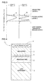
- Fig. 1 is a schematic front cross-sectional view showing a boundary acoustic wave device according to a first embodiment of the present invention.
- a boundary acoustic wave device 1 includes a piezoelectric layer 2, a dielectric layer 3 laminated on the piezoelectric layer 2, a low thermal expansion medium layer 4 laminated on a surface of the piezoelectric layer 2 opposite to the surface on which the dielectric layer 3 is provided, and an IDT electrode 5 provided at the boundary between the piezoelectric layer 2 and the dielectric layer 3.
- the boundary acoustic wave device 1 of this embodiment uses a SH boundary acoustic wave that propagates at the boundary between the piezoelectric layer 2 and the dielectric layer 3.
- the piezoelectric layer 2 may use piezoelectric single crystal, such as LiTaO 3 , LibO 3 , or quartz crystal.
- the dielectric layer 3 may use an inorganic dielectric material such as SiO 2 , or an organic dielectric material.
- the low thermal expansion medium layer 4 is made of a material with a linear thermal expansion coefficient less than that of the piezoelectric layer 2.
- a material may be, for example, Si, sapphire, or SiN.
- This embodiment features that an acoustic velocity of the SH wave in the piezoelectric layer 2 in a boundary acoustic wave propagation direction satisfies Expression (1), and when ⁇ represents a wavelength of the IDT electrode 5, a relationship among (an acoustic velocity of a transverse wave in the dielectric layer)/ ⁇ , a response frequency of the boundary acoustic wave, and a response frequency of a high order mode of the boundary acoustic wave, satisfies Expression (2) as follows:
- a transverse wave in a dielectric layer and "a transverse wave in a low thermal expansion medium layer” are S waves if these materials are not anisotropic, or these transverse waves are SH transverse waves if these materials are anisotropic.
- the expressions "the acoustic velocity of the transverse wave in the dielectric layer” and “the acoustic velocity of the transverse wave in the low thermal expansion medium layer” cover both of S waves and SH transverse waves.
- the acoustic velocities of the SH wave, SV wave, S wave, P wave, etc., in the boundary acoustic wave propagation direction are respectively uniquely determined depending on the materials. Representative values of the acoustic velocities in the materials to be used as the piezoelectric layer, the dielectric layer, and the low thermal expansion medium layer are shown in Table 1, which will be provided later.
- the dielectric layer 3 has a surface 3a with irregularities at the side opposite to the boundary between the piezoelectric layer 2 and the dielectric layer 3.
- the irregularities scatter the high order mode of the boundary acoustic wave propagating toward the surface 3a, so as to further decrease the effect of the high order mode spurious response on the resonance characteristic and filter characteristic.
- the surface 3a may be a rough surface, or organic or inorganic particles may adhere onto the surface 3a.
- the boundary acoustic wave device 1 of this embodiment includes the low thermal expansion medium layer 4, and satisfies Expressions (1) and (2) described above. Thus, the high order mode spurious response can be decreased.
- the low thermal expansion medium layer 4 has a linear thermal expansion coefficient less than that of the piezoelectric layer 2. Accordingly, deformation of the boundary acoustic wave device 1 with temperature changes is decreased, thereby improving a temperature characteristic. It is desirable that such a material with the smaller linear thermal expansion coefficient has a rigidity capable of suppressing expansion of the piezoelectric layer.
- the material of the low thermal expansion medium layer 4 may be preferably a material, such as Si, sapphire, or SiN, which allows a SH or Stoneley transverse wave to propagate at a high acoustic velocity.
- Fig. 2 is an illustration schematically showing an energy distribution of a boundary acoustic wave when the vertical axis plots a position in a thickness direction of the boundary acoustic wave device 1.
- the horizontal axis in Fig. 2 represents that vibration energy of the boundary acoustic wave increases toward the right side.
- the energy distribution of the SH boundary acoustic wave to be used teaches that the energy most increases at the boundary between the piezoelectric layer 2 and the dielectric layer 3, and rapidly decreases as the position shifts away from the boundary.
- the energy of the boundary acoustic wave does not substantially reach the low thermal expansion medium layer 4.
- the boundary acoustic wave can propagate around the boundary between the piezoelectric layer 2 and the dielectric layer 3.
- Fig. 3 is an illustration schematically showing an energy distribution of a high order mode which should be suppressed. Distributions of a high order mode A indicated by arrow A and a high order mode B indicated by arrow B both exhibit distributions of high energy within the piezoelectric layer 2. Thus, the high order modes A and B propagate while being substantially enclosed in the piezoelectric layer 2. A condition of the high order modes A and B propagating while being substantially enclosed in the piezoelectric layer 2 is that acoustic velocities of the high order modes are lower than the acoustic velocities of the transverse waves in the dielectric layer 3 and the low thermal expansion medium layer 4.
- the dielectric layer 3 is arranged on the IDT electrode 5.
- the boundary acoustic wave can propagate without a loss because no leakage occurs as long as the acoustic velocity of the SH wave in the piezoelectric layer 2 and the acoustic velocity of the transverse wave in the dielectric layer 3 are higher than the acoustic velocity of the boundary acoustic wave to be used.
- the acoustic velocity of a SH wave and the acoustic velocity of a longitudinal wave in the piezoelectric layer 2 are higher than the acoustic velocity of the boundary acoustic wave, and hence, the high order mode in which a transverse wave and a longitudinal wave propagate as main components while being coupled to each other and being enclosed in the piezoelectric layer 2 generally has a higher acoustic velocity than that of the boundary acoustic wave.
- the acoustic velocity of the transverse wave in the dielectric layer is lower than the acoustic velocity of the SH wave in the piezoelectric layer 2 and the acoustic velocity of the transverse wave in the low thermal expansion medium layer 4. That is, the piezoelectric layer 2, the dielectric layer 3, and the low thermal expansion medium layer 4 are formed to satisfy the relationship of Expression (1). Also, since the acoustic velocity of the transverse wave in the dielectric layer 3 is set between the acoustic velocity of the boundary acoustic wave and the acoustic velocity of the high order mode, that is, since Expression (2) is satisfied, the SH boundary acoustic wave to be used propagates without a loss. The high order mode which may cause a spurious response can be attenuated as a leaky wave that leaks to the dielectric layer 3.
- the high order mode spurious response can be decreased, and a good resonance characteristic and filter characteristic can be provided.
- Boundary acoustic waves include a SH boundary acoustic wave mainly having a SH component and a Stoneley wave mainly having P+SV components, i.e., a P+SV boundary acoustic wave.
- the SH boundary acoustic wave and the Stoneley wave may propagate while respectively having only the SH component and the P+SV components.
- piezoelectric single crystal such as LiTaO 3 or LiNbO 3 , which is anisotropic crystal, is used as the piezoelectric layer, the three components of P, SH, and SV are typically coupled to each other and then propagate in many substrate directions of the piezoelectric layer.
- the boundary acoustic wave device 1 is assumingly configured such that the piezoelectric layer 2 uses Y-cut X-propagation LiTaO 3 , the dielectric layer 3 uses SiO 2 the lower thermal expansion medium layer uses polycrystalline Si, and the IDT electrode 5 uses an Au film with a sufficient thickness.
- an SH boundary acoustic wave propagates at the boundary between the piezoelectric layer 2 and the dielectric layer 3.
- the acoustic velocity of the shear vertical wave, or SV wave is 3351 m/sec, which is lower than the acoustic velocity of the transverse wave in SiO 2 of 3757 m/sec.
- the energy of the SV component of the high order mode leaks to the dielectric layer 3, and the high order mode can be diffused.
- the acoustic velocity of the SH wave (main component) is 4227 m/sec, which is higher than the acoustic velocity of the transverse wave in SiO 2 .
- the energy of the SH component of the high order mode has difficulty in leaking, and hence, it is difficult to reliably attenuate the energy.
- the high order mode mainly having the SH component is highly excited. Therefore, the high order mode mainly having the SH component is preferably attenuated as a leaky wave.
- the transverse wave in the piezoelectric layer may be preferably a SH wave.
- the transverse wave may be preferably a SV wave.
- the acoustic velocity of the SV wave in the piezoelectric layer may preferably satisfy Expression (3), and when ⁇ represents the wavelength of the IDT electrode, a response frequency of the Stoneley boundary acoustic wave, a response frequency of the high order mode of the boundary acoustic wave, and the acoustic velocity of the transverse wave in the dielectric layer may preferably satisfy a range defined by Expression (4) as follows:
- transverse waves in Expressions (3) and (4) are S waves when the materials of the dielectric layer and the low thermal expansion medium layer are not anisotropic.
- the transverse waves are SV waves when the materials are anisotropic. That is, the above-mentioned "transverse wave” includes the SV wave if the material is anisotropic, in addition to the transverse wave, which is the S wave.
- the dielectric layer 3 and the piezoelectric layer 2 may be made of insulating materials like this embodiment.
- the dielectric layer 3 and the piezoelectric layer 2 are made of semiconductors, electric current flows from the IDT electrode 5 to the semiconductors, and an electroacoustic conversion performance of the IDT electrode 5 may be deteriorated.
- the dielectric layer 3 and the piezoelectric layer 2 are made of insulating materials, the electroacoustic conversion performance of the IDT electrode 5 is hardly deteriorated.
- the electric characteristic of the boundary acoustic wave device for example, a resonant resistance or an anti-resonant resistance, or an insertion loss is hardly deteriorated.
- a resistance at a portion between electrodes connected to different potentials of the IDT electrode 5 may be 10 k ⁇ or higher.
- Fig. 4 is a schematic front cross-sectional view showing a boundary acoustic wave device 11 according to a second embodiment of the present invention.
- Fig. 5 is a schematic front cross-sectional view showing a boundary acoustic wave device 21 prepared as a comparative example.
- boundary acoustic wave devices 11 and 21 will be described with reference to specific examples to clarify the structure and advantage of the boundary acoustic wave device 11 of this embodiment.
- the boundary acoustic wave device 11 includes a piezoelectric layer 2, a dielectric layer 3, and a low thermal expansion medium layer 4 laminated on a surface of the piezoelectric layer 2 opposite to the boundary between the piezoelectric layer 2 and the dielectric layer 3, in a similar manner to the boundary acoustic wave device 1.
- An IDT electrode 5 is formed at the boundary between the piezoelectric layer 2 and the dielectric layer 3.
- a sound absorbing layer 6 is laminated on a surface 3a of the dielectric layer 3 opposite to the boundary.
- the boundary acoustic wave device 11 is configured to satisfy Expressions (1) and (2) mentioned above. Therefore, a high order mode of a boundary acoustic wave leaks to the dielectric layer 3, and a high order mode spurious response caused by the high order mode is decreased. In contrast, a SH or Stoneley boundary acoustic wave to be used propagates around the boundary substantially without a loss, and hence, a good resonance characteristic and a good filter characteristic can be provided.
- the sound absorbing layer 6 since the sound absorbing layer 6 is provided, the sound absorbing layer 6 absorbs the high order mode propagating to the surface 3a of the dielectric layer 3. Accordingly, the high order mode spurious response can be decreased.
- the material of the sound absorbing layer 6 is not particularly limited as long as the material can absorb the high order mode.
- the material may be an organic material such as synthetic resin, or a porous inorganic material, such as porous silica, porous alumina, porous titanium oxide, porous glass, porous magnesia (MgO), or porous aluminum.
- the synthetic resin may be, for example, polyimide, silicone resin, or epoxy resin.
- the thickness of the sound absorbing layer 6 is not particularly limited as long as the sound absorbing layer 6 can absorb the propagating high order mode. To reliably absorb the high order mode, the thickness is preferably 1.0 ⁇ or greater. If the thickness of the sound absorbing layer 6 is too large, the thickness of the boundary acoustic wave device 11 may become too large. It is not desirable. Thus, the thickness of the sound absorbing layer 6 may be preferably 200 ⁇ m or less.
- the boundary acoustic wave device 11 was manufactured with specifications as follows:
- piezoelectric layer 2 of 15° Y-cut X-propagation LiNbO 3 being 4 ⁇ thick; dielectric layer 3 of SiO 2 being 5 ⁇ thick and having irregularities at surface 3a;
- the boundary acoustic wave device 21 shown in Fig. 5 was manufactured.
- the boundary acoustic wave device 21 includes an IDT electrode 25 at the interface between a piezoelectric layer 22 and a dielectric layer 23.
- a low thermal expansion medium layer 24 is laminated on a surface 23a of the dielectric layer 23 opposite to the boundary between the piezoelectric layer 22 and the dielectric layer 23.
- a sound absorbing layer 26 is laminated on a surface 22a of the piezoelectric layer 22 opposite to the boundary.
- the IDT electrode 25 was formed on the piezoelectric layer, and a dielectric film was formed so as to cover the IDT electrode. Then, the dielectric film was polished by CMP, and the polished dielectric layer surface and the surface of the low thermal expansion medium layer 24 were activated and bonded with each other.
- the specifications of the boundary acoustic wave 21 are as follows:
- the IDT electrode 25 was provided to define a one-port boundary acoustic wave resonator.
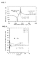
- Fig. 7 shows an impedance characteristic of the boundary acoustic wave device 11 of the embodiment manufactured as described above.
- Fig. 6 shows an impedance characteristic of the boundary acoustic wave device 21 of the comparative example.
- the boundary acoustic wave device of the comparative example generates a noticeable high order mode spurious response.
- the boundary acoustic wave device 21 has a noticeably large high order mode spurious response although the thickness of the piezoelectric layer 22 is sufficiently large, the irregularities are provided at the surface 22a of the piezoelectric layer 22, and the sound absorbing layer 26 is laminated.
- the boundary acoustic wave device 11 of the embodiment generates only a small high order mode spurious response.
- Fig. 8 is a schematic illustration showing an energy distribution of a SH boundary wave in the embodiment or the boundary acoustic wave device 21 of the comparative example.
- the vertical axis plots a position in a thickness direction of the boundary acoustic wave device 21, in which 0.0 represents the boundary between the piezoelectric layer 22 and the dielectric layer 23.
- the horizontal axis plots energy (a standardized value). The standardized value of the energy is standardized while the largest energy is defined as 1.0.
- a vibration mode is non-leaky mode, that is, without a propagation loss.
- character reference U1 denotes a P component of the boundary acoustic wave
- U2 denotes a SH component
- U3 denotes a SV component.
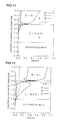
- Figs. 9 and 10 are schematic illustrations showing an energy distribution of a high order mode spurious response of the boundary acoustic wave device 21 of the above-described comparative example.
- character reference U1 denotes a P component of the high order mode
- U2 denotes a SH component
- U3 denotes a SV component.
- Vibration of the high order mode is concentrated at the dielectric layer 23. The largest shift appears in the dielectric layer 23. Vibration is evanescently attenuated at the piezoelectric layer 22 and the low thermal expansion medium layer 24. It is thus found that the vibration is in a non-leaky vibration mode. Therefore, it is difficult to attenuate the high order mode although the thickness of the piezoelectric layer is increased as large as 125 ⁇ , the irregularities are provided at the surface of the piezoelectric layer 22, and the sound absorbing layer 26 is formed.
- Figs. 11 and 12 show an energy distribution of a high order mode spurious response of the boundary acoustic wave device according to the embodiment.
- the energy distribution of the SH boundary wave, which is a main mode, is similar to that in Fig. 8 provided as the comparative example.
- character reference U1 denotes a P component
- U2 denotes a SH component
- U3 denotes a SV component.
- the vibration of the high order mode is not concentrated at the piezoelectric layer 2, and it leaks to the dielectric layer 3. Therefore, it is found that the vibration is in the leaky vibration mode. Accordingly, in the above-described embodiment, since the high order mode leaks to the surface of the dielectric layer 3 opposite to the boundary, and the irregularities are provided at the surface 3a of the dielectric layer 3, the high order mode is scattered, and also absorbed by the sound absorbing layer 6. The high order mode spurious response can be effectively suppressed.
- Table 1 shows acoustic velocities of transverse waves in media of the boundary acoustic wave device 11 of the embodiment, and those of the boundary acoustic wave device 21 of the comparative example.
- a high order mode spurious response is generated when the value of a frequency ⁇ of the high order mode spurious response is greater than the acoustic velocity of the transverse wave in SiO 2 defining the dielectric layer, i.e., the acoustic velocity of the S wave of 3757 m/sec.
- a high order mode spurious response is slightly generated when the value of a frequency ⁇ of the high order mode spurious response is greater than the acoustic velocity of the transverse wave in LiNbO 3 , i.e., the acoustic velocity of the SV wave of 4031 m/sec.
- the occurrence of the high order mode spurious generated by the IDT electrode is restricted by the acoustic velocity of the medium. Accordingly, with the embodiment, since the acoustic velocity of the transverse wave in the piezoelectric layer 2 is lower than the acoustic velocity of the transverse wave in the dielectric layer 3, the high order mode spurious response occurs when frequency ⁇ is greater than the acoustic velocity of the dielectric layer 3, the high order mode spurious response can define the leaky wave. While the boundary acoustic wave device 11 of the second embodiment uses the SH boundary wave for example, the boundary acoustic wave device 11 may use a Stoneley boundary acoustic wave in a similar manner to the first embodiment.
- the boundary acoustic wave device of the present invention has the layer structure including (the sound absorbing layer provided if necessary,) the dielectric layer, the IDT electrode, the piezoelectric layer, and the low thermal expansion medium layer, that is, since the device has the relatively simple layer structure, the high order mode spurious response can be effectively suppressed. Also, by laminating the low thermal expansion medium layer, characteristic changes with temperature changes can be decreased. Thus, when an oscillation circuit is formed by using the boundary acoustic wave resonator of the present invention, the occurrence of abnormal vibration is remarkably decreased. Also, when a band-pass filter is defined by the boundary acoustic wave device of the present invention, a high order mode spurious response is hardly generated, thereby providing a good filter characteristic.
- a sound absorbing layer 7 may be additionally provided between the piezoelectric layer 2 and the low thermal expansion medium layer 4 as shown in Fig. 13 .
- the sound absorbing layer 7 is arranged, in order to transmit a stress from the low thermal expansion medium layer 4 to the piezoelectric layer 2, it is desirable that the sound absorbing layer 7 is thin or that the sound absorbing layer 7 is made of a hard material.
- the sound absorbing layer 7 is made of a resin material with a Young's modulus of several Gpa, such as epoxy resin, it is desirable that the thickness of the sound absorbing layer 7 is several ⁇ or less.
- the sound absorbing layer 7 may be made of a material being as hard as SOG (spin-on glass) and having a lower density than that of SiO 2 . Still alternatively, the sound absorbing layer 7 may be formed of a structure in which metal is dispersed at the interface between the piezoelectric layer 2 and the low thermal expansion medium layer 4 and a crystal structure at the interface portion is broken.
- the above-described piezoelectric layer 2 may be made of other material, for example, ZnO, Ta 2 O 5 , PZT, AIN, LiTaO 3 , or KN.
- the above-described dielectric layer 3 may be formed of other material, for example, SiO 2 , SiC, Al 2 O 3 , DLC, ZnO, Ta 2 O 5 , PZT, AlN, LiTaO 3 , or KN.
- the material of the low thermal expansion medium layer 4 is not limited to the above-mentioned polycrystalline Si, and may be other material, such as polycrystalline Si, SiC, Al 2 O 3 , Al 2 O 3 , sapphire, or diamond like carbon (DLC).
- polycrystalline Si SiC
- Al 2 O 3 Al 2 O 3
- sapphire Al 2 O 3
- DLC diamond like carbon
- the low thermal expansion medium layer 4 may be bonded and joined to the piezoelectric layer 2.
- the material of the low thermal expansion medium layer may be formed by a film-forming method.
- a film-forming method may be sputtering, CVD, depositing, coating, or the like.
- a protection layer may be additionally formed on the outer side of the layer structure including (the sound absorbing layer provided if necessary,) the dielectric layer, the IDT electrode, the piezoelectric layer, and the low thermal expansion medium layer.
- the material of the protection layer is not particularly limited, and may be an insulating material, for example, synthetic resin, such as polyimide or epoxy resin, or an inorganic material, such as titanium oxide, aluminum nitride, or aluminum oxide.
- the protection layer may be formed of a metal film made of, for example, Au, Al or W.
- boundary acoustic wave device of the present invention may be enclosed in other package with or without the above-described protection layer.
Landscapes
- Physics & Mathematics (AREA)
- Acoustics & Sound (AREA)
- Surface Acoustic Wave Elements And Circuit Networks Thereof (AREA)
Abstract
A boundary acoustic wave device capable of effectively suppressing a high order mode spurious response with a relatively simple structure is provided. A boundary acoustic wave device (1) includes an IDT electrode (5) between a piezoelectric layer (2) and a dielectric layer (3). A low thermal expansion medium layer (4) made of a material having a linear thermal expansion coefficient less than that of the piezoelectric layer (2) is laminated on a surface of the piezoelectric layer 2 opposite to the boundary. Acoustic velocities of transversal waves in a boundary acoustic wave propagation direction at the piezoelectric layer (2), the dielectric layer (3), and the low thermal expansion medium layer (4) satisfy Expression (1), and when λ represents a wavelength of the IDT electrode (5), (an acoustic velocity of a transverse wave at the dielectric layer)/λ satisfies Expression (2) as follows: 

Description
- The present invention relates to a boundary acoustic wave device applied to, for example, a resonator or a band-pass filter. More particularly, the present invention relates to a boundary acoustic wave device using a boundary acoustic wave that propagates at the boundary between a piezoelectric layer and a dielectric layer.
- Conventionally, a surface acoustic wave device has been widely applied to a band-pass filter of a mobile phone or the like. For example, Patent Document 1 (listed below) discloses a surface acoustic wave filter.
Fig. 14 briefly illustrates a sectional structure of the filter. - A surface acoustic wave filter 501 shown in
Fig. 14 includes apiezoelectric layer 502 made of LiTaO3, and anIDT electrode 503 formed on thepiezoelectric layer 502. Sapphire 504 is joined to the back surface of thepiezoelectric layer 502 opposite to a surface on which theIDT electrode 503 is formed. Assuming that T is a thickness of thepiezoelectric layer 502 and λ is a wavelength of a surface acoustic wave to be used, a ratio T/λ of the thickness of thepiezoelectric layer 502 to the wavelength λ of the surface acoustic wave is 10 or greater. Accordingly, a spurious response is decreased, which is generated by reflection of a bulk acoustic wave (BAW) at the boundary surface between thepiezoelectric layer 502 and thesapphire 504. - Recently, a boundary acoustic wave device has been suggested instead of the surface acoustic wave device. The boundary acoustic wave device uses a boundary acoustic wave that propagates at the boundary between a piezoelectric layer and a dielectric layer. In the surface acoustic wave device, to excite the IDT electrode formed on the surface of the piezoelectric layer, a gap has to be provided so as not to interrupt vibration. Hence, the surface acoustic wave device may have a complicated and large package structure. In contrast, the boundary acoustic wave device uses the boundary acoustic wave that propagates at the boundary between the piezoelectric layer and the dielectric layer. A gap is not required. Hence, the boundary acoustic wave device may have a simple and small package.
- Also, Patent Document 2 (listed below) discloses a boundary acoustic wave device having a layer structure including a sound absorbing medium, SiO2, an IDT electrode, and LiNbO3. Here, an acoustic velocity of a transverse wave in the sound absorbing medium is lower than an acoustic velocity of a transverse wave in SiO2. The sound absorbing medium is made of epoxy resin or porous SiO2. It is described that a high order mode spurious response is suppressed by providing the sound absorbing medium.
- Also, Patent Document 3 (listed below) discloses a boundary acoustic wave device having a layer structure including a polycrystalline silicon film, a polycrystalline silicon oxide film, an IDT, and a single crystal piezoelectric substrate. Here, since the polycrystalline silicon film is formed, a boundary acoustic wave excited at the IDT electrode is enclosed in a portion before the polycrystalline silicon oxide film. It is also described that the IDT electrode is reliably protected by the polycrystalline silicon film and the polycrystalline silicon oxide film.
- Further, Patent Document 4 (listed below) discloses a boundary acoustic wave device in which an IDT electrode is arranged at the boundary between a piezoelectric layer and a dielectric layer and which uses a SH boundary acoustic wave. Here, the thickness of the IDT electrode is determined such that an acoustic velocity of the SH boundary wave is lower than acoustic velocities of transverse waves propagating in the dielectric layer and the piezoelectric layer. With this structure, an electromechanical coupling coefficient may be large, a propagation loss and a power flow angle may be small, and a temperature coefficient of frequency TCF may be set within a proper range.
- Patent Document 1: Japanese Unexamined Patent Application Publication No.
2004-186868 - Patent Document 2: Japanese Unexamined Patent Application Publication (Translation of PCT Application) No.
2005/069486 - Patent Document 3: Japanese Unexamined Patent Application Publication (Translation of PCT Application) No.
98/52279 - Patent Document 4: Japanese Unexamined Patent Application Publication (Translation of PCT Application) No.
2004/070946 - In the boundary acoustic wave device, it is demanded to suppress a higher order mode spurious response more than the mode of the boundary acoustic wave to be used.
- As described in
Patent Document 1, the surface acoustic wave device can decrease the high order mode spurious response as long as a solid such as sapphire is bonded to the surface of the piezoelectric layer opposite to the surface on which the IDT electrode is formed, and the ratio of the thickness of the piezoelectric layer to the wavelength of the surface wave is within a specific range. -
Patent Document 1 discloses an example in paragraphs (0036) to (0042) in which an IDT electrode is formed on the front surface of 42° Y-cut X-propagation LiTaO3, and an R-plane cut sapphire substrate is laminated on the back surface of the LiTaO3. In this configuration, a first leaky surface wave mainly having an SH component propagates on the front surface of the LiTaO3 substrate. Paragraph (0034) ofPatent Document 1 describes that, with the above-described structure, a spurious response may be generated by reflection of BAW at the boundary surface between the LiTaO3 and the sapphire substrate. - In contrast, based on the knowledge of the inventor of the subject application, a spurious response generated under the condition is a high order propagation mode in which a P wave, a SH wave, and a SV wave propagate in a coupled manner. An acoustic velocity of the SV wave propagating in a propagation direction in the LiTaO3 with this cut direction is 3351 m/s, and an acoustic velocity of the SH wave is 4277 m/s. An acoustic velocity of a transverse wave in the sapphire is 6463 m/s. Since the acoustic velocity of the transverse wave in the sapphire is higher than the acoustic velocity of the SH wave in the LiTaO3, a high order mode spurious response mainly having a SH component and a high order mode spurious response mainly having a P+SV components are generated at the boundary between the sapphire and the LiTaO3. The 42° Y-cut X-propagation LiTaO3 substrate causes the SH wave to be strongly excited. Hence, a high order mode spurious response mainly having a SH component is strongly generated.
-
Patent Document 1 decreases the high order mode spurious response by increasing the thickness of the LiTaO3 substrate. - However, regarding
Patent Document 1, when a frequency characteristic ofFig. 6 in a case where the LiTaO3 substrate has a small thickness is compared with a frequency characteristic ofFig. 10 in a case where the LiTaO3 substrate has a large thickness, it is found that a spurious response is more suppressed in the case ofFig. 10 ofPatent Document 1 than the case ofFig. 6 ofPatent Document 1. However, the number of appearances of spurious responses is increased. Namely, excitation intensity in a high order mode which may cause the spurious response is decreased by increasing the thickness of the LiTaO3 substrate; however, high order modes of many orders would be enclosed. Thus, a filter characteristic of the surface wave device is not sufficiently improved. - Regarding
Patent Document 2, the sound absorbing medium with an acoustic velocity of a transverse wave lower than the acoustic velocity of the transverse wave in the SiO2 is formed on the SiO2. Accordingly, the high order mode can be decreased. However, a resin material, such as epoxy resin, polyimide, or liquid crystal polymer, which is used as the sound absorbing medium has a high linear thermal expansion coefficient. If the rigidity of the structure including the SiO2, the IDT, and the LiNbO3 for propagation of the boundary acoustic wave is not sufficient, the structure may be likely expanded or contracted in accordance with the temperature of the boundary acoustic wave device on account of the effect applied by the linear thermal expansion coefficient of the sound absorbing medium. Thus, the absolute value of the temperature coefficient of frequency TCF of the boundary acoustic wave device may be increased. - With the boundary acoustic wave device disclosed in
Patent Document 3, the piezoelectric single crystal substrate made of, for example, LiNbO3, is bonded with Si with a small thermal expansion coefficient. Accordingly, the absolute value of the temperature coefficient of frequency TCF can be decreased. In this case, by providing SiO2, which is a low acoustic velocity material, arranged between the Si and the LiNbO3 which are high acoustic velocity materials, a main propagation mode of the boundary acoustic wave is enclosed within the SiO2 region. - With the boundary acoustic wave device disclosed in
Patent Document 4, in a case where metal such as Au heavier than Al is used instead of Al which is as light as SiO2, vibration energy in a main mode of the boundary acoustic wave does not spread over the entire SiO2, but is concentrated at the piezoelectric substrate. Thus, an electromechanical coupling coefficient K2 of the boundary acoustic wave can be increased. - However, with the structure in which the low acoustic velocity medium is arranged between the high acoustic velocity media like the boundary acoustic wave device disclosed in
Patent Document 3, the acoustic velocity may vary depending on the thickness and film quality of the low acoustic velocity medium. As a result, a frequency variation may appear in the boundary acoustic wave device. Thus, precise quality control for the thickness and film quality of the low acoustic velocity medium is necessary. - By increasing the thickness of the low acoustic velocity medium, the effect of variation in energy distribution in the main mode of the boundary acoustic wave due to the variation in thickness of the low acoustic velocity medium can be decreased. However, if the thickness of the low acoustic velocity medium is increased, a high order mode spurious response may be generated.
- As described in
Patent Documents 2 to 4, in the conventional boundary acoustic wave devices, various suggestions have been made to suppress the high order mode spurious response, to increase the electromechanical coupling coefficient, and to decrease the absolute value of the temperature coefficient of frequency TCF. Unlike the surface acoustic wave device, with the boundary acoustic wave device, the high order mode spurious response is not sufficiently decreased. - In light of the situation, an object of the present invention is to provide a boundary acoustic wave device which can effectively decrease a response intensity of a high order mode spurious response with a relatively simple structure without significantly increasing the number of responses unlike the conventional technique, and which can provide a good filter characteristic and a good resonance characteristic.
- According to a first invention of the subject application, a boundary acoustic wave device includes a piezoelectric layer, a dielectric layer laminated on the piezoelectric layer, an IDT electrode arranged at the interface between the piezoelectric layer and the dielectric layer, and a low thermal expansion medium layer laminated on a surface of the piezoelectric layer opposite to the interface and made of a material having a linear thermal expansion coefficient less than that of the piezoelectric layer. The boundary acoustic wave device uses a SH boundary acoustic wave propagating at the boundary between the piezoelectric layer and the dielectric layer. An acoustic velocity of a SH wave in the piezoelectric layer satisfies Expression (1), and when λ represents a wavelength of the IDT electrode, (an acoustic velocity of a transverse wave in the dielectric layer)/λ with respect to a response frequency of the SH boundary acoustic wave and to a response frequency in a high order mode satisfies a range defined by Expression (2) as follows:
-


-


- In the present invention, preferably, the piezoelectric layer has a thickness within a range of from 1λ to 50λ. Herein, the thickness of the piezoelectric layer represents a dimension in a lamination direction in which the piezoelectric layer and the dielectric layer are laminated.
- Energy of vibration of the boundary acoustic wave to be used is mainly distributed within a range of from the boundary between the piezoelectric layer and the dielectric layer to a depth of 1λ of the piezoelectric layer. Hence, when the boundary acoustic wave propagates, the thickness of the piezoelectric layer may be preferably 1λ or greater. If the thickness of the piezoelectric layer is less than 1λ, the energy distribution of the boundary acoustic wave may reach the low thermal expansion medium layer, and hence frequency variations may be increased depending on a condition of the interface joining (bonding) the piezoelectric layer and the low thermal expansion medium layer and variation in thickness of the piezoelectric layer.
- The overall linear thermal expansion coefficient of the boundary acoustic wave device is determined by a ratio of thicknesses of the piezoelectric layer, the dielectric layer, and the low thermal expansion medium layer. If the thickness of the piezoelectric layer is 50λ or less, the piezoelectric layer is not too large. Hence, the overall linear thermal expansion coefficient of the boundary acoustic wave device can be decreased, thereby decreasing the thickness of the low thermal expansion medium layer. Accordingly, the boundary acoustic wave device with an entirely decreased thickness and having a good temperature characteristic can be provided.
- Preferably, a sound absorbing layer is provided on a surface of the dielectric layer opposite to the boundary. Accordingly, the sound absorbing layer absorbs a high order mode spurious response which leaks to the surface of the dielectric layer opposite to the boundary. The high order mode spurious response can be further effectively suppressed.
- Also, preferably, a structure for scattering an elastic wave is provided at the surface of the dielectric layer opposite to the boundary. In this case, since the elastic wave leaking to the surface of the dielectric layer opposite to the boundary is scattered, the high order mode spurious response can be further effectively suppressed. The structure for scattering the elastic wave may be configured such that the surface of the dielectric layer opposite to the boundary is a rough surface, irregularities are formed at that surface, or inorganic or organic particles adhere onto that surface.
- Preferably, a sound absorbing layer is provided between the piezoelectric layer and the low thermal expansion medium layer. In this case, the sound absorbing layer can absorb the high order mode leaking to the surface of the piezoelectric layer opposite to the boundary. Accordingly, the high order mode spurious response can be further effectively suppressed.
- In the present invention, preferably, the piezoelectric layer and the dielectric layer are formed of insulating materials. If the piezoelectric layer and the dielectric layer are formed of insulating materials, an electroacoustic conversion characteristic of the IDT electrode is hardly deteriorated. Accordingly, in a case of a boundary acoustic wave resonator, a resonance characteristic or an antiresonance characteristic are hardly deteriorated, and in a case of a boundary acoustic wave filter, a loss is hardly increased. In particular, the piezoelectric layer and the dielectric layer are media in contact with the IDT electrode. When these media are semiconductor materials such as Si, electric current flows through the media. This may deteriorate the electroacoustic conversion characteristic of the IDT electrode. In contrast, when the piezoelectric layer and the dielectric layer are formed of insulating materials, the electroacoustic conversion performance of the IDT electrode is hardly deteriorated. Preferably, a resistance between IDT electrode portions connected to different potentials may be 10 kΩ or higher.
- With the boundary acoustic wave device according to the first invention, since the low thermal expansion medium layer is laminated on the surface of the piezoelectric layer opposite to the boundary, the relationship among the acoustic velocities of the SH transverse waves in the boundary wave propagation direction at the piezoelectric layer, the dielectric layer, and the low thermal expansion medium layer satisfies Expression (1), and (the acoustic velocity of the transverse wave at the dielectric layer)/λ satisfies Expression (2), the high order mode spurious response can be effectively decreased. The reason is as follows.
- The high order mode is generated when the acoustic velocity of the transverse wave in the piezoelectric layer is lower than the acoustic velocity of the transverse wave in the dielectric layer, and when the acoustic velocity of the SH wave in the piezoelectric layer is lower than the acoustic velocity of the transverse wave in the low thermal expansion medium layer. Otherwise, the high order mode leaks from the piezoelectric layer to the periphery. In contrast, when the acoustic velocity of the boundary acoustic wave is lower than those of the transverse waves in the piezoelectric layer and the dielectric layer, the boundary acoustic wave can propagate without a loss. Accordingly, as long as Expressions (1) and (2) are satisfied, the boundary acoustic wave can propagate without a loss, the high order mode can leak from the piezoelectric layer to the periphery, and hence, the high order mode spurious response can be effectively decreased.
- Similarly, with the second invention, since the relationship among the acoustic velocities of the SV transverse waves in the boundary wave propagation direction in the piezoelectric layer, the dielectric layer, and the low thermal expansion medium layer satisfies Expression (3), and (the acoustic velocity of the transverse wave at the dielectric layer)/λ satisfies Expression (4), the Stoneley boundary acoustic wave can be used while the high order mode of the Stoneley boundary acoustic wave can be effectively suppressed.
- Therefore, with the first and second inventions, the boundary acoustic wave device can be provided, which can effectively suppress the high order mode spurious response by using a relatively simple structure in which the piezoelectric layer and the dielectric layer are laminated, and the low thermal expansion medium layer is laminated on the surface of the piezoelectric layer opposite to the boundary, and which can provide a good resonance characteristic and a good filter characteristic.
-
- [
Fig. 1] Fig. 1 is a schematic front cross-sectional view showing a boundary acoustic wave device according to a first embodiment of the present invention. - [
Fig. 2] Fig. 2 is an illustration schematically showing an energy distribution of a SH boundary acoustic wave of the boundary acoustic wave device according to the first embodiment. - [
Fig. 3] Fig. 3 is an illustration schematically showing an energy distribution in a high order mode which may cause a spurious response. - [
Fig. 4] Fig. 4 is a schematic front cross-sectional view showing a boundary acoustic wave device according to a second embodiment of the present invention. - [
Fig. 5] Fig. 5 is a schematic front cross-sectional view showing a boundary acoustic wave device prepared as a comparative example. - [
Fig. 6] Fig. 6 is an illustration showing an impedance characteristic of the boundary acoustic wave device as the comparative example shown inFig. 5 . - [
Fig. 7] Fig. 7 is an illustration showing an impedance characteristic of the boundary acoustic wave device according to the second embodiment. - [
Fig. 8] Fig. 8 is an illustration schematically showing an energy distribution of a SH boundary acoustic wave of the boundary acoustic wave device according to the comparative example or the second embodiment. - [
Fig. 9] Fig. 9 is an illustration schematically showing an energy distribution of a high order mode of the boundary acoustic wave device according to the comparative example. - [
Fig. 10] Fig. 10 is an illustration schematically showing an energy distribution of a high order mode of the boundary acoustic wave device according to the comparative example. - [
Fig. 11] Fig. 11 is an illustration schematically showing an energy distribution of a high order mode of the boundary acoustic wave device according to the second embodiment. - [
Fig. 12] Fig. 12 is an illustration schematically showing an energy distribution of a high order mode of the boundary acoustic wave device according to the second embodiment. - [
Fig. 13] Fig. 13 is a schematic front cross-sectional view showing a modification of the boundary acoustic wave device according to the second embodiment. - [
Fig. 14] Fig. 14 is a schematic front cross-sectional view showing an example of a conventional surface acoustic wave device. -
- 1
- boundary acoustic wave device
- 2
- piezoelectric layer
- 3
- dielectric layer
- 4
- low thermal expansion medium layer
- 5
- IDT electrode
- 6
- sound absorbing layer
- 7
- sound absorbing layer
- 11
- boundary acoustic wave device
- Specific embodiments of the present invention will now be described with reference to the attached drawings to clarify the present invention.
-
Fig. 1 is a schematic front cross-sectional view showing a boundary acoustic wave device according to a first embodiment of the present invention. - A boundary
acoustic wave device 1 includes apiezoelectric layer 2, adielectric layer 3 laminated on thepiezoelectric layer 2, a low thermalexpansion medium layer 4 laminated on a surface of thepiezoelectric layer 2 opposite to the surface on which thedielectric layer 3 is provided, and anIDT electrode 5 provided at the boundary between thepiezoelectric layer 2 and thedielectric layer 3. The boundaryacoustic wave device 1 of this embodiment uses a SH boundary acoustic wave that propagates at the boundary between thepiezoelectric layer 2 and thedielectric layer 3. - The
piezoelectric layer 2 may use piezoelectric single crystal, such as LiTaO3, LibO3, or quartz crystal. - The
dielectric layer 3 may use an inorganic dielectric material such as SiO2, or an organic dielectric material. - The low thermal
expansion medium layer 4 is made of a material with a linear thermal expansion coefficient less than that of thepiezoelectric layer 2. Such a material may be, for example, Si, sapphire, or SiN. - This embodiment features that an acoustic velocity of the SH wave in the
piezoelectric layer 2 in a boundary acoustic wave propagation direction satisfies Expression (1), and when λ represents a wavelength of theIDT electrode 5, a relationship among (an acoustic velocity of a transverse wave in the dielectric layer)/λ, a response frequency of the boundary acoustic wave, and a response frequency of a high order mode of the boundary acoustic wave, satisfies Expression (2) as follows: -


Herein, it is assumed that "a transverse wave in a dielectric layer" and "a transverse wave in a low thermal expansion medium layer" are S waves if these materials are not anisotropic, or these transverse waves are SH transverse waves if these materials are anisotropic. Also, it is assumed that the expressions "the acoustic velocity of the transverse wave in the dielectric layer" and "the acoustic velocity of the transverse wave in the low thermal expansion medium layer" cover both of S waves and SH transverse waves. - The acoustic velocities of the SH wave, SV wave, S wave, P wave, etc., in the boundary acoustic wave propagation direction are respectively uniquely determined depending on the materials. Representative values of the acoustic velocities in the materials to be used as the piezoelectric layer, the dielectric layer, and the low thermal expansion medium layer are shown in Table 1, which will be provided later.
- In Expression (2), (acoustic velocity of transverse wave in dielectric layer)/λ < (frequency response of high order mode) is a condition that cuts off the high order mode. The high order mode cannot be suppressed unless the condition is satisfied.
- In this embodiment, the
dielectric layer 3 has a surface 3a with irregularities at the side opposite to the boundary between thepiezoelectric layer 2 and thedielectric layer 3. The irregularities scatter the high order mode of the boundary acoustic wave propagating toward the surface 3a, so as to further decrease the effect of the high order mode spurious response on the resonance characteristic and filter characteristic. - Instead of providing the irregularities, various structures may be used for scattering the high order mode. For example, the surface 3a may be a rough surface, or organic or inorganic particles may adhere onto the surface 3a.
- The boundary
acoustic wave device 1 of this embodiment includes the low thermalexpansion medium layer 4, and satisfies Expressions (1) and (2) described above. Thus, the high order mode spurious response can be decreased. - The low thermal
expansion medium layer 4 has a linear thermal expansion coefficient less than that of thepiezoelectric layer 2. Accordingly, deformation of the boundaryacoustic wave device 1 with temperature changes is decreased, thereby improving a temperature characteristic. It is desirable that such a material with the smaller linear thermal expansion coefficient has a rigidity capable of suppressing expansion of the piezoelectric layer. Hence, the material of the low thermalexpansion medium layer 4 may be preferably a material, such as Si, sapphire, or SiN, which allows a SH or Stoneley transverse wave to propagate at a high acoustic velocity. -
Fig. 2 is an illustration schematically showing an energy distribution of a boundary acoustic wave when the vertical axis plots a position in a thickness direction of the boundaryacoustic wave device 1. The horizontal axis inFig. 2 represents that vibration energy of the boundary acoustic wave increases toward the right side. Referring toFig. 2 , the energy distribution of the SH boundary acoustic wave to be used teaches that the energy most increases at the boundary between thepiezoelectric layer 2 and thedielectric layer 3, and rapidly decreases as the position shifts away from the boundary. The energy of the boundary acoustic wave does not substantially reach the low thermalexpansion medium layer 4. Hence, the boundary acoustic wave can propagate around the boundary between thepiezoelectric layer 2 and thedielectric layer 3. -
Fig. 3 is an illustration schematically showing an energy distribution of a high order mode which should be suppressed. Distributions of a high order mode A indicated by arrow A and a high order mode B indicated by arrow B both exhibit distributions of high energy within thepiezoelectric layer 2. Thus, the high order modes A and B propagate while being substantially enclosed in thepiezoelectric layer 2. A condition of the high order modes A and B propagating while being substantially enclosed in thepiezoelectric layer 2 is that acoustic velocities of the high order modes are lower than the acoustic velocities of the transverse waves in thedielectric layer 3 and the low thermalexpansion medium layer 4. - With the surface acoustic wave device described in
Patent Document 1, no dielectric layer is present on an IDT electrode. Thus, the acoustic velocity in a space above an upper surface of thepiezoelectric layer 502 is approximately infinite. The high order mode propagates while being substantially enclosed in the boundary between the piezoelectric layer and the space above the piezoelectric layer, i.e., on the surface of the piezoelectric layer. - In contrast, with the boundary
acoustic wave device 1, thedielectric layer 3 is arranged on theIDT electrode 5. Here, in the case of the boundary acoustic wave device mainly using the SH component, the boundary acoustic wave can propagate without a loss because no leakage occurs as long as the acoustic velocity of the SH wave in thepiezoelectric layer 2 and the acoustic velocity of the transverse wave in thedielectric layer 3 are higher than the acoustic velocity of the boundary acoustic wave to be used. Meanwhile, the acoustic velocity of a SH wave and the acoustic velocity of a longitudinal wave in thepiezoelectric layer 2 are higher than the acoustic velocity of the boundary acoustic wave, and hence, the high order mode in which a transverse wave and a longitudinal wave propagate as main components while being coupled to each other and being enclosed in thepiezoelectric layer 2 generally has a higher acoustic velocity than that of the boundary acoustic wave. - In this embodiment, the acoustic velocity of the transverse wave in the dielectric layer is lower than the acoustic velocity of the SH wave in the
piezoelectric layer 2 and the acoustic velocity of the transverse wave in the low thermalexpansion medium layer 4. That is, thepiezoelectric layer 2, thedielectric layer 3, and the low thermalexpansion medium layer 4 are formed to satisfy the relationship of Expression (1). Also, since the acoustic velocity of the transverse wave in thedielectric layer 3 is set between the acoustic velocity of the boundary acoustic wave and the acoustic velocity of the high order mode, that is, since Expression (2) is satisfied, the SH boundary acoustic wave to be used propagates without a loss. The high order mode which may cause a spurious response can be attenuated as a leaky wave that leaks to thedielectric layer 3. - With this embodiment, the high order mode spurious response can be decreased, and a good resonance characteristic and filter characteristic can be provided.
- Boundary acoustic waves include a SH boundary acoustic wave mainly having a SH component and a Stoneley wave mainly having P+SV components, i.e., a P+SV boundary acoustic wave. The SH boundary acoustic wave and the Stoneley wave may propagate while respectively having only the SH component and the P+SV components. If piezoelectric single crystal, such as LiTaO3 or LiNbO3, which is anisotropic crystal, is used as the piezoelectric layer, the three components of P, SH, and SV are typically coupled to each other and then propagate in many substrate directions of the piezoelectric layer.
- For example, the boundary
acoustic wave device 1 is assumingly configured such that thepiezoelectric layer 2 uses Y-cut X-propagation LiTaO3, thedielectric layer 3 uses SiO2 the lower thermal expansion medium layer uses polycrystalline Si, and theIDT electrode 5 uses an Au film with a sufficient thickness. In such a case, an SH boundary acoustic wave propagates at the boundary between thepiezoelectric layer 2 and thedielectric layer 3. The acoustic velocity of the shear vertical wave, or SV wave is 3351 m/sec, which is lower than the acoustic velocity of the transverse wave in SiO2 of 3757 m/sec. Accordingly, energy of the SV component of the high order mode leaks to thedielectric layer 3, and the high order mode can be diffused. However, the acoustic velocity of the SH wave (main component) is 4227 m/sec, which is higher than the acoustic velocity of the transverse wave in SiO2. The energy of the SH component of the high order mode has difficulty in leaking, and hence, it is difficult to reliably attenuate the energy. - In the condition of propagation of the SH boundary acoustic wave, the high order mode mainly having the SH component is highly excited. Therefore, the high order mode mainly having the SH component is preferably attenuated as a leaky wave. When the SH boundary acoustic wave is used, the transverse wave in the piezoelectric layer may be preferably a SH wave. When the Stoneley boundary acoustic wave is used, the transverse wave may be preferably a SV wave.
- If the Stoneley boundary acoustic wave is used, the acoustic velocity of the SV wave in the piezoelectric layer may preferably satisfy Expression (3), and when λ represents the wavelength of the IDT electrode, a response frequency of the Stoneley boundary acoustic wave, a response frequency of the high order mode of the boundary acoustic wave, and the acoustic velocity of the transverse wave in the dielectric layer may preferably satisfy a range defined by Expression (4) as follows:
-


- Preferably, the
dielectric layer 3 and thepiezoelectric layer 2 may be made of insulating materials like this embodiment. When thedielectric layer 3 and thepiezoelectric layer 2 are made of semiconductors, electric current flows from theIDT electrode 5 to the semiconductors, and an electroacoustic conversion performance of theIDT electrode 5 may be deteriorated. In contrast, when thedielectric layer 3 and thepiezoelectric layer 2 are made of insulating materials, the electroacoustic conversion performance of theIDT electrode 5 is hardly deteriorated. Hence, the electric characteristic of the boundary acoustic wave device, for example, a resonant resistance or an anti-resonant resistance, or an insertion loss is hardly deteriorated. More preferably, a resistance at a portion between electrodes connected to different potentials of theIDT electrode 5 may be 10 kΩ or higher. -
Fig. 4 is a schematic front cross-sectional view showing a boundaryacoustic wave device 11 according to a second embodiment of the present invention.Fig. 5 is a schematic front cross-sectional view showing a boundaryacoustic wave device 21 prepared as a comparative example. - The boundary
acoustic wave devices acoustic wave device 11 of this embodiment. - Referring to
Fig. 4 , the boundaryacoustic wave device 11 includes apiezoelectric layer 2, adielectric layer 3, and a low thermalexpansion medium layer 4 laminated on a surface of thepiezoelectric layer 2 opposite to the boundary between thepiezoelectric layer 2 and thedielectric layer 3, in a similar manner to the boundaryacoustic wave device 1. AnIDT electrode 5 is formed at the boundary between thepiezoelectric layer 2 and thedielectric layer 3. Further, in this embodiment, asound absorbing layer 6 is laminated on a surface 3a of thedielectric layer 3 opposite to the boundary. - In this embodiment, the boundary
acoustic wave device 11 is configured to satisfy Expressions (1) and (2) mentioned above. Therefore, a high order mode of a boundary acoustic wave leaks to thedielectric layer 3, and a high order mode spurious response caused by the high order mode is decreased. In contrast, a SH or Stoneley boundary acoustic wave to be used propagates around the boundary substantially without a loss, and hence, a good resonance characteristic and a good filter characteristic can be provided. - In addition, in this embodiment, since the
sound absorbing layer 6 is provided, thesound absorbing layer 6 absorbs the high order mode propagating to the surface 3a of thedielectric layer 3. Accordingly, the high order mode spurious response can be decreased. The material of thesound absorbing layer 6 is not particularly limited as long as the material can absorb the high order mode. For example, the material may be an organic material such as synthetic resin, or a porous inorganic material, such as porous silica, porous alumina, porous titanium oxide, porous glass, porous magnesia (MgO), or porous aluminum. The synthetic resin may be, for example, polyimide, silicone resin, or epoxy resin. - The thickness of the
sound absorbing layer 6 is not particularly limited as long as thesound absorbing layer 6 can absorb the propagating high order mode. To reliably absorb the high order mode, the thickness is preferably 1.0λ or greater. If the thickness of thesound absorbing layer 6 is too large, the thickness of the boundaryacoustic wave device 11 may become too large. It is not desirable. Thus, the thickness of thesound absorbing layer 6 may be preferably 200 µm or less. - Next, an advantage of the boundary
acoustic wave device 11 having thesound absorbing layer 6, in which the high order mode is effectively suppressed, is described with reference to the specific example. - The boundary
acoustic wave device 11 was manufactured with specifications as follows: -
piezoelectric layer 2 of 15° Y-cut X-propagation LiNbO3 being 4λ thick;dielectric layer 3 of SiO2 being 5λ thick and having irregularities at surface 3a; - low thermal
expansion medium layer 4 of polycrystalline Si being 50λ thick;
sound absorbinglayer 6 of polyimide being 3λ thick; and
IDT electrode of Au being 0.05λ thick and having 0.6 duty ratio.
For comparison, a boundaryacoustic wave device 21 shown inFig. 5 was manufactured. The boundaryacoustic wave device 21 includes anIDT electrode 25 at the interface between apiezoelectric layer 22 and adielectric layer 23. A low thermalexpansion medium layer 24 is laminated on a surface 23a of thedielectric layer 23 opposite to the boundary between thepiezoelectric layer 22 and thedielectric layer 23. Further, asound absorbing layer 26 is laminated on a surface 22a of thepiezoelectric layer 22 opposite to the boundary. During manufacturing, theIDT electrode 25 was formed on the piezoelectric layer, and a dielectric film was formed so as to cover the IDT electrode. Then, the dielectric film was polished by CMP, and the polished dielectric layer surface and the surface of the low thermalexpansion medium layer 24 were activated and bonded with each other. - The specifications of the boundary
acoustic wave 21 are as follows: -
Piezoelectric layer 22 of 15° Y-cut X-propagation LiNbO3 being 125λ thick,
irregularities being provided at a surface of thepiezoelectric layer 22 opposite to the side formed with theIDT electrode 25; -
dielectric layer 23 of SiO2 being 4λ, thick;
low thermalexpansion medium layer 24 of polycrystalline Si being 10λ thick;
sound absorbinglayer 26 of polyimide; and
IDT electrode 25 of Au being 0.05λ thick and having 0.6 duty.
In the boundaryacoustic wave device 11 of the above-described embodiment and the boundaryacoustic wave device 21 of the comparative example, theIDT electrode -
Fig. 7 shows an impedance characteristic of the boundaryacoustic wave device 11 of the embodiment manufactured as described above.Fig. 6 shows an impedance characteristic of the boundaryacoustic wave device 21 of the comparative example. As shown inFig. 6 , the boundary acoustic wave device of the comparative example generates a noticeable high order mode spurious response. In particular, the boundaryacoustic wave device 21 has a noticeably large high order mode spurious response although the thickness of thepiezoelectric layer 22 is sufficiently large, the irregularities are provided at the surface 22a of thepiezoelectric layer 22, and thesound absorbing layer 26 is laminated. - In contrast, as shown in
Fig. 7 , the boundaryacoustic wave device 11 of the embodiment generates only a small high order mode spurious response. -
Fig. 8 is a schematic illustration showing an energy distribution of a SH boundary wave in the embodiment or the boundaryacoustic wave device 21 of the comparative example. InFig. 8 , the vertical axis plots a position in a thickness direction of the boundaryacoustic wave device 21, in which 0.0 represents the boundary between thepiezoelectric layer 22 and thedielectric layer 23. The horizontal axis plots energy (a standardized value). The standardized value of the energy is standardized while the largest energy is defined as 1.0. - As shown in
Fig. 8 , vibration is concentrated at the boundary portion of thepiezoelectric layer 22 and thedielectric layer 23 provided with the IDT electrode. Since the largest displacement appears at this portion, and the vibration is evanescently attenuated at thepiezoelectric layer 22 and thedielectric layer 23, it is found that a vibration mode is non-leaky mode, that is, without a propagation loss. InFig. 8 , character reference U1 denotes a P component of the boundary acoustic wave, U2 denotes a SH component, and U3 denotes a SV component. -
Figs. 9 and 10 are schematic illustrations showing an energy distribution of a high order mode spurious response of the boundaryacoustic wave device 21 of the above-described comparative example. Also, inFigs. 9 and 10 , character reference U1 denotes a P component of the high order mode, U2 denotes a SH component, and U3 denotes a SV component. Vibration of the high order mode is concentrated at thedielectric layer 23. The largest shift appears in thedielectric layer 23. Vibration is evanescently attenuated at thepiezoelectric layer 22 and the low thermalexpansion medium layer 24. It is thus found that the vibration is in a non-leaky vibration mode. Therefore, it is difficult to attenuate the high order mode although the thickness of the piezoelectric layer is increased as large as 125λ, the irregularities are provided at the surface of thepiezoelectric layer 22, and thesound absorbing layer 26 is formed. - On the other hand,
Figs. 11 and 12 show an energy distribution of a high order mode spurious response of the boundary acoustic wave device according to the embodiment. The energy distribution of the SH boundary wave, which is a main mode, is similar to that inFig. 8 provided as the comparative example. - Also, in
Figs. 11 and 12 , character reference U1 denotes a P component, U2 denotes a SH component, and U3 denotes a SV component. - As shown in
Figs. 11 and 12 , the vibration of the high order mode is not concentrated at thepiezoelectric layer 2, and it leaks to thedielectric layer 3. Therefore, it is found that the vibration is in the leaky vibration mode. Accordingly, in the above-described embodiment, since the high order mode leaks to the surface of thedielectric layer 3 opposite to the boundary, and the irregularities are provided at the surface 3a of thedielectric layer 3, the high order mode is scattered, and also absorbed by thesound absorbing layer 6. The high order mode spurious response can be effectively suppressed. - Table 1 shows acoustic velocities of transverse waves in media of the boundary
acoustic wave device 11 of the embodiment, and those of the boundaryacoustic wave device 21 of the comparative example. -
[Table 1] SV wave (m/s) SH wave (m/s) S wave (m/s) P wave (m/s) LiNbO3 4031 4752 - 6547 Au - - 1245 3378 SiO2 - - 3757 5960 Polycrystalline Si - - 5341 8945 - In the boundary
acoustic wave device 11 of the comparative example, a high order mode spurious response is generated when the value of a frequency×λ of the high order mode spurious response is greater than the acoustic velocity of the transverse wave in SiO2 defining the dielectric layer, i.e., the acoustic velocity of the S wave of 3757 m/sec. In the boundaryacoustic wave device 11 of the embodiment, a high order mode spurious response is slightly generated when the value of a frequency×λ of the high order mode spurious response is greater than the acoustic velocity of the transverse wave in LiNbO3, i.e., the acoustic velocity of the SV wave of 4031 m/sec. - As described above, the occurrence of the high order mode spurious generated by the IDT electrode is restricted by the acoustic velocity of the medium. Accordingly, with the embodiment, since the acoustic velocity of the transverse wave in the
piezoelectric layer 2 is lower than the acoustic velocity of the transverse wave in thedielectric layer 3, the high order mode spurious response occurs when frequency×λ is greater than the acoustic velocity of thedielectric layer 3, the high order mode spurious response can define the leaky wave. While the boundaryacoustic wave device 11 of the second embodiment uses the SH boundary wave for example, the boundaryacoustic wave device 11 may use a Stoneley boundary acoustic wave in a similar manner to the first embodiment. - As described above, since the boundary acoustic wave device of the present invention has the layer structure including (the sound absorbing layer provided if necessary,) the dielectric layer, the IDT electrode, the piezoelectric layer, and the low thermal expansion medium layer, that is, since the device has the relatively simple layer structure, the high order mode spurious response can be effectively suppressed. Also, by laminating the low thermal expansion medium layer, characteristic changes with temperature changes can be decreased. Thus, when an oscillation circuit is formed by using the boundary acoustic wave resonator of the present invention, the occurrence of abnormal vibration is remarkably decreased. Also, when a band-pass filter is defined by the boundary acoustic wave device of the present invention, a high order mode spurious response is hardly generated, thereby providing a good filter characteristic.
- While the low thermal
expansion medium layer 4 is directly laminated on thepiezoelectric layer 2 in the first and second embodiments, asound absorbing layer 7 may be additionally provided between thepiezoelectric layer 2 and the low thermalexpansion medium layer 4 as shown inFig. 13 . When thesound absorbing layer 7 is arranged, in order to transmit a stress from the low thermalexpansion medium layer 4 to thepiezoelectric layer 2, it is desirable that thesound absorbing layer 7 is thin or that thesound absorbing layer 7 is made of a hard material. Thus, when thesound absorbing layer 7 is made of a resin material with a Young's modulus of several Gpa, such as epoxy resin, it is desirable that the thickness of thesound absorbing layer 7 is several λ or less. Alternatively, thesound absorbing layer 7 may be made of a material being as hard as SOG (spin-on glass) and having a lower density than that of SiO2. Still alternatively, thesound absorbing layer 7 may be formed of a structure in which metal is dispersed at the interface between thepiezoelectric layer 2 and the low thermalexpansion medium layer 4 and a crystal structure at the interface portion is broken. - The above-described
piezoelectric layer 2 may be made of other material, for example, ZnO, Ta2O5, PZT, AIN, LiTaO3, or KN. The above-describeddielectric layer 3 may be formed of other material, for example, SiO2, SiC, Al2O3, DLC, ZnO, Ta2O5, PZT, AlN, LiTaO3, or KN. - Also, the material of the low thermal
expansion medium layer 4 is not limited to the above-mentioned polycrystalline Si, and may be other material, such as polycrystalline Si, SiC, Al2O3, Al2O3, sapphire, or diamond like carbon (DLC). - Further, the low thermal
expansion medium layer 4 may be bonded and joined to thepiezoelectric layer 2. Alternatively, the material of the low thermal expansion medium layer may be formed by a film-forming method. Such a film-forming method may be sputtering, CVD, depositing, coating, or the like. - Further, in the boundary acoustic wave device of the present invention, a protection layer may be additionally formed on the outer side of the layer structure including (the sound absorbing layer provided if necessary,) the dielectric layer, the IDT electrode, the piezoelectric layer, and the low thermal expansion medium layer. By forming the protection layer, the strength of the boundary acoustic wave device can be increased, and corrosive gas can be prevented from entering. The material of the protection layer is not particularly limited, and may be an insulating material, for example, synthetic resin, such as polyimide or epoxy resin, or an inorganic material, such as titanium oxide, aluminum nitride, or aluminum oxide. Alternatively, the protection layer may be formed of a metal film made of, for example, Au, Al or W.
- Further, the boundary acoustic wave device of the present invention may be enclosed in other package with or without the above-described protection layer.
Claims (7)
- A boundary acoustic wave device comprising:a piezoelectric layer;a dielectric layer laminated on the piezoelectric layer;an IDT electrode arranged at the interface between the piezoelectric layer and the dielectric layer; anda low thermal expansion medium layer laminated on a surface of the piezoelectric layer opposite to the interface and made of a material having a linear thermal expansion coefficient less than that of the piezoelectric layer,wherein the boundary acoustic wave device uses a SH boundary acoustic wave propagating at the boundary between the piezoelectric layer and the dielectric layer, and
wherein an acoustic velocity of a SH wave in the piezoelectric layer satisfies Expression (1), and when λ represents a wavelength of the IDT electrode, (an acoustic velocity of a transverse wave in the dielectric layer)/λ with respect to a response frequency of the SH boundary acoustic wave and to a response frequency in a high order mode satisfies Expression (2) as follows:

- A boundary acoustic wave device comprising:a piezoelectric layer;a dielectric layer laminated on the piezoelectric layer;an IDT electrode arranged at the interface between the piezoelectric layer and the dielectric layer; anda low thermal expansion medium layer laminated on a surface of the piezoelectric layer opposite to a surface on which the IDT electrode is formed and made of a material having a linear thermal expansion coefficient less than that of the piezoelectric layer,wherein the boundary acoustic wave device uses a Stoneley boundary acoustic wave propagating at the boundary between the piezoelectric layer and the dielectric layer, and
wherein an acoustic velocity of a SV wave in the piezoelectric layer satisfies Expression (3), and when λ represents a wavelength of the IDT electrode, (an acoustic velocity of a transverse wave at the dielectric layer)/λ with respect to a response frequency of the Stoneley boundary acoustic wave and to a response frequency in a high order mode satisfies Expression (4) as follows:

- The boundary acoustic wave device according to claim 1 or 2, wherein the piezoelectric layer has a thickness within a range of from 1λ to 50λ.
- The boundary acoustic wave device according to any one of claims 1 to 3,
wherein a sound absorbing layer is laminated on a surface of the dielectric layer opposite to the boundary. - The boundary acoustic wave device according to any one of claims 1 to 4,
wherein a structure for scattering an elastic wave propagating to the surface of the dielectric layer opposite to the boundary is provided at that surface. - The boundary acoustic wave device according to any one of claims 1 to 5, further comprising a sound absorbing layer provided between the piezoelectric layer and the low thermal expansion medium layer.
- The boundary acoustic wave device according to any one of claims 1 to 6,
wherein the piezoelectric layer and the dielectric layer are formed of insulating materials.
Applications Claiming Priority (2)
| Application Number | Priority Date | Filing Date | Title |
|---|---|---|---|
| JP2006347575 | 2006-12-25 | ||
| PCT/JP2007/072559 WO2008078481A1 (en) | 2006-12-25 | 2007-11-21 | Elastic boundary-wave device |
Publications (2)
| Publication Number | Publication Date |
|---|---|
| EP2104228A1 true EP2104228A1 (en) | 2009-09-23 |
| EP2104228A4 EP2104228A4 (en) | 2014-10-08 |
Family
ID=39562274
Family Applications (1)
| Application Number | Title | Priority Date | Filing Date |
|---|---|---|---|
| EP07832289.8A Withdrawn EP2104228A4 (en) | 2006-12-25 | 2007-11-21 | ELASTIC LIMIT WAVE DEVICE |
Country Status (5)
| Country | Link |
|---|---|
| US (1) | US8049395B2 (en) |
| EP (1) | EP2104228A4 (en) |
| JP (1) | JP4894861B2 (en) |
| CN (1) | CN101569100A (en) |
| WO (1) | WO2008078481A1 (en) |
Cited By (1)
| Publication number | Priority date | Publication date | Assignee | Title |
|---|---|---|---|---|
| FR3042647A1 (en) * | 2015-10-20 | 2017-04-21 | Soitec Silicon On Insulator | COMPOSITE STRUCTURE AND METHOD OF MANUFACTURING THE SAME |
Families Citing this family (30)
| Publication number | Priority date | Publication date | Assignee | Title |
|---|---|---|---|---|
| US8470019B1 (en) * | 2001-11-30 | 2013-06-25 | Advanced Cardiovascular Systems, Inc. | TiNxOy modified surface for an implantable device and a method of producing the same |
| EP2131192A1 (en) * | 2007-03-29 | 2009-12-09 | Murata Manufacturing Co. Ltd. | Sensor for detecting substance in liquid |
| JP5041004B2 (en) * | 2007-10-23 | 2012-10-03 | パナソニック株式会社 | Boundary acoustic wave device |
| JP5392258B2 (en) * | 2008-07-11 | 2014-01-22 | パナソニック株式会社 | Sheet wave element and electronic device using the same |
| WO2010016246A1 (en) * | 2008-08-07 | 2010-02-11 | パナソニック株式会社 | Elastic wave element and electronic device using the same |
| JP2010068503A (en) * | 2008-08-13 | 2010-03-25 | Seiko Epson Corp | Surface acoustic wave element |
| CN102204094B (en) * | 2008-11-10 | 2014-01-15 | 松下电器产业株式会社 | Elastic wave element and electronic device using the same |
| JP5218566B2 (en) * | 2009-01-07 | 2013-06-26 | 株式会社村田製作所 | Boundary acoustic wave device |
| WO2011007690A1 (en) * | 2009-07-17 | 2011-01-20 | 株式会社村田製作所 | Surface acoustic wave device |
| WO2011030519A1 (en) * | 2009-09-11 | 2011-03-17 | パナソニック株式会社 | Acoustic wave element and acoustic wave element sensor |
| JP5299521B2 (en) * | 2009-12-15 | 2013-09-25 | 株式会社村田製作所 | Boundary acoustic wave device |
| WO2013047433A1 (en) * | 2011-09-30 | 2013-04-04 | 株式会社村田製作所 | Elastic wave device |
| JP5861771B2 (en) * | 2012-03-26 | 2016-02-16 | 株式会社村田製作所 | Elastic wave device and manufacturing method thereof |
| WO2014034326A1 (en) * | 2012-08-29 | 2014-03-06 | 株式会社村田製作所 | Elastic wave apparatus |
| FR3004289B1 (en) * | 2013-04-08 | 2015-05-15 | Soitec Silicon On Insulator | SURFACE ACOUSTIC WAVE COMPONENT AND METHOD OF MANUFACTURING THE SAME |
| JP6447624B2 (en) * | 2014-03-14 | 2019-01-09 | 株式会社村田製作所 | Elastic wave device |
| DE112015001771B4 (en) * | 2014-04-11 | 2019-05-23 | Murata Manufacturing Co., Ltd. | Filter device for elastic waves |
| CN107005225B (en) * | 2014-12-25 | 2021-06-04 | 株式会社村田制作所 | elastic wave device |
| US10574203B2 (en) | 2015-07-28 | 2020-02-25 | Qorvo Us, Inc. | Bonded wafers and surface acoustic wave devices using same |
| US10128814B2 (en) * | 2016-01-28 | 2018-11-13 | Qorvo Us, Inc. | Guided surface acoustic wave device providing spurious mode rejection |
| CN109690943B (en) * | 2016-09-20 | 2023-10-13 | 日本碍子株式会社 | Composite substrate, manufacturing method and electronic device |
| WO2018151146A1 (en) * | 2017-02-16 | 2018-08-23 | 株式会社弾性波デバイスラボ | Acoustic wave element and method for manufacturing same |
| DE102017012407B3 (en) | 2017-05-24 | 2023-03-30 | RF360 Europe GmbH | SAW device with suppressed spurious mode signals |
| DE102017111448B4 (en) | 2017-05-24 | 2022-02-10 | RF360 Europe GmbH | SAW device with suppressed spurious mode signals |
| US11206007B2 (en) | 2017-10-23 | 2021-12-21 | Qorvo Us, Inc. | Quartz orientation for guided SAW devices |
| CN111373766A (en) | 2017-11-21 | 2020-07-03 | 日东电工株式会社 | Piezoelectric loudspeaker |
| JP6913619B2 (en) * | 2017-12-12 | 2021-08-04 | 株式会社村田製作所 | Multiplexers, high frequency front-end circuits and communication equipment |
| JP7292100B2 (en) * | 2019-05-16 | 2023-06-16 | NDK SAW devices株式会社 | Surface acoustic wave devices, filter circuits and electronic components |
| CN112865742B (en) * | 2019-11-12 | 2025-10-28 | 华景传感科技(无锡)有限公司 | Bulk Acoustic Wave Resonator |
| JP7509598B2 (en) * | 2020-07-29 | 2024-07-02 | 太陽誘電株式会社 | Acoustic Wave Devices, Filters and Multiplexers |
Family Cites Families (15)
| Publication number | Priority date | Publication date | Assignee | Title |
|---|---|---|---|---|
| JP3132065B2 (en) * | 1991-08-08 | 2001-02-05 | 住友電気工業株式会社 | Surface acoustic wave device and method of manufacturing the same |
| JPH0595249A (en) | 1991-10-02 | 1993-04-16 | Tdk Corp | Surface acoustic wave element |
| US6046656A (en) * | 1997-05-08 | 2000-04-04 | Kabushiki Kaisha Toshiba | Elastic boundary wave device and method of its manufacture |
| WO1998052279A1 (en) | 1997-05-12 | 1998-11-19 | Hitachi, Ltd. | Elastic wave device |
| JP3090810U (en) | 2002-06-18 | 2002-12-26 | 財団法人工業技術研究院 | Structure of layered surface acoustic wave filter |
| JP2004186868A (en) * | 2002-12-02 | 2004-07-02 | Fujitsu Media Device Kk | Surface acoustic wave element, transmission filter and reception filter having the same, and duplexer having the same |
| EP2139110A1 (en) * | 2003-02-10 | 2009-12-30 | Murata Manufacturing Co. Ltd. | Boundary acoustic wave device |
| JP3774782B2 (en) * | 2003-05-14 | 2006-05-17 | 富士通メディアデバイス株式会社 | Manufacturing method of surface acoustic wave device |
| JP4483785B2 (en) * | 2004-01-13 | 2010-06-16 | 株式会社村田製作所 | Boundary acoustic wave device |
| US7486001B2 (en) * | 2004-01-19 | 2009-02-03 | Murata Manufacturing Co., Ltd. | Boundary acoustic wave device |
| WO2005099091A1 (en) * | 2004-04-08 | 2005-10-20 | Murata Manufacturing Co., Ltd. | Elastic boundary wave filter |
| EP1879291A4 (en) | 2005-04-25 | 2012-02-22 | Murata Manufacturing Co | Boundary acoustic wave device |
| JP4937605B2 (en) * | 2006-03-07 | 2012-05-23 | 太陽誘電株式会社 | Boundary acoustic wave device |
| JP4917396B2 (en) * | 2006-09-25 | 2012-04-18 | 太陽誘電株式会社 | Filters and duplexers |
| JP4920750B2 (en) * | 2007-08-14 | 2012-04-18 | 太陽誘電株式会社 | Boundary acoustic wave device |
-
2007
- 2007-11-21 EP EP07832289.8A patent/EP2104228A4/en not_active Withdrawn
- 2007-11-21 CN CNA2007800481461A patent/CN101569100A/en active Pending
- 2007-11-21 JP JP2008550998A patent/JP4894861B2/en active Active
- 2007-11-21 WO PCT/JP2007/072559 patent/WO2008078481A1/en not_active Ceased
-
2009
- 2009-06-11 US US12/482,604 patent/US8049395B2/en active Active
Cited By (3)
| Publication number | Priority date | Publication date | Assignee | Title |
|---|---|---|---|---|
| FR3042647A1 (en) * | 2015-10-20 | 2017-04-21 | Soitec Silicon On Insulator | COMPOSITE STRUCTURE AND METHOD OF MANUFACTURING THE SAME |
| WO2017068270A1 (en) * | 2015-10-20 | 2017-04-27 | Soitec | Composite structure and associated production method |
| US12603629B2 (en) | 2015-10-20 | 2026-04-14 | Soitec | Composite structure and associated production method |
Also Published As
| Publication number | Publication date |
|---|---|
| US20090236935A1 (en) | 2009-09-24 |
| JP4894861B2 (en) | 2012-03-14 |
| JPWO2008078481A1 (en) | 2010-04-15 |
| EP2104228A4 (en) | 2014-10-08 |
| US8049395B2 (en) | 2011-11-01 |
| CN101569100A (en) | 2009-10-28 |
| WO2008078481A1 (en) | 2008-07-03 |
Similar Documents
| Publication | Publication Date | Title |
|---|---|---|
| US8049395B2 (en) | Boundary acoustic wave device | |
| CN111953309B (en) | Surface acoustic wave element, filter circuit, and electronic component | |
| JP4894911B2 (en) | Boundary acoustic wave filter | |
| EP1635459B1 (en) | Acoustic boundary wave device | |
| JP5392258B2 (en) | Sheet wave element and electronic device using the same | |
| JP4356613B2 (en) | Boundary acoustic wave device | |
| EP2773040B1 (en) | Surface acoustic wave device | |
| US7522020B2 (en) | Boundary acoustic wave device and method for manufacturing boundary acoustic wave device | |
| JP3892370B2 (en) | Surface acoustic wave element, filter device, and manufacturing method thereof | |
| US7323803B2 (en) | Boundary acoustic wave device | |
| KR20190077224A (en) | Elastic wave device | |
| EP2763315A1 (en) | Elastic wave device | |
| US7355319B2 (en) | Boundary acoustic wave device | |
| WO2005060094A1 (en) | Acoustic boundary wave device | |
| CN114070257B (en) | Acoustic wave devices, filters and multiplexers | |
| KR102667725B1 (en) | elastic wave device | |
| US6437479B1 (en) | Surface acoustic wave device | |
| US12149228B2 (en) | Acoustic wave device, wafer, and method of manufacturing wafer | |
| JP2023166577A (en) | Acoustic wave element | |
| JP7577559B2 (en) | Acoustic Wave Devices, Wafers, Filters and Multiplexers | |
| JP2025135988A (en) | Acoustic wave device, filter, and method for manufacturing an acoustic wave device | |
| CN119892001A (en) | Surface acoustic wave resonator and manufacturing method thereof |
Legal Events
| Date | Code | Title | Description |
|---|---|---|---|
| PUAI | Public reference made under article 153(3) epc to a published international application that has entered the european phase |
Free format text: ORIGINAL CODE: 0009012 |
|
| 17P | Request for examination filed |
Effective date: 20090625 |
|
| AK | Designated contracting states |
Kind code of ref document: A1 Designated state(s): AT BE BG CH CY CZ DE DK EE ES FI FR GB GR HU IE IS IT LI LT LU LV MC MT NL PL PT RO SE SI SK TR |
|
| DAX | Request for extension of the european patent (deleted) | ||
| A4 | Supplementary search report drawn up and despatched |
Effective date: 20140908 |
|
| RIC1 | Information provided on ipc code assigned before grant |
Ipc: H03H 9/02 20060101AFI20140902BHEP |
|
| STAA | Information on the status of an ep patent application or granted ep patent |
Free format text: STATUS: THE APPLICATION IS DEEMED TO BE WITHDRAWN |
|
| 18D | Application deemed to be withdrawn |
Effective date: 20150408 |