EP2158597B1 - Monolithisches induktives bauelement, verfahren zum herstellen des bauelements und verwendung des bauelements - Google Patents
Monolithisches induktives bauelement, verfahren zum herstellen des bauelements und verwendung des bauelements Download PDFInfo
- Publication number
- EP2158597B1 EP2158597B1 EP08761143A EP08761143A EP2158597B1 EP 2158597 B1 EP2158597 B1 EP 2158597B1 EP 08761143 A EP08761143 A EP 08761143A EP 08761143 A EP08761143 A EP 08761143A EP 2158597 B1 EP2158597 B1 EP 2158597B1
- Authority
- EP
- European Patent Office
- Prior art keywords
- green
- ferritic
- component
- core material
- encapsulation
- Prior art date
- Legal status (The legal status is an assumption and is not a legal conclusion. Google has not performed a legal analysis and makes no representation as to the accuracy of the status listed.)
- Not-in-force
Links
Images

Classifications
-
- H—ELECTRICITY
- H01—ELECTRIC ELEMENTS
- H01F—MAGNETS; INDUCTANCES; TRANSFORMERS; SELECTION OF MATERIALS FOR THEIR MAGNETIC PROPERTIES
- H01F17/00—Fixed inductances of the signal type
- H01F17/0006—Printed inductances
- H01F17/0013—Printed inductances with stacked layers
-
- H—ELECTRICITY
- H01—ELECTRIC ELEMENTS
- H01F—MAGNETS; INDUCTANCES; TRANSFORMERS; SELECTION OF MATERIALS FOR THEIR MAGNETIC PROPERTIES
- H01F41/00—Apparatus or processes specially adapted for manufacturing or assembling magnets, inductances or transformers; Apparatus or processes specially adapted for manufacturing materials characterised by their magnetic properties
- H01F41/02—Apparatus or processes specially adapted for manufacturing or assembling magnets, inductances or transformers; Apparatus or processes specially adapted for manufacturing materials characterised by their magnetic properties for manufacturing cores, coils, or magnets
- H01F41/0206—Manufacturing of magnetic cores by mechanical means
- H01F41/0246—Manufacturing of magnetic circuits by moulding or by pressing powder
-
- H—ELECTRICITY
- H01—ELECTRIC ELEMENTS
- H01F—MAGNETS; INDUCTANCES; TRANSFORMERS; SELECTION OF MATERIALS FOR THEIR MAGNETIC PROPERTIES
- H01F41/00—Apparatus or processes specially adapted for manufacturing or assembling magnets, inductances or transformers; Apparatus or processes specially adapted for manufacturing materials characterised by their magnetic properties
- H01F41/02—Apparatus or processes specially adapted for manufacturing or assembling magnets, inductances or transformers; Apparatus or processes specially adapted for manufacturing materials characterised by their magnetic properties for manufacturing cores, coils, or magnets
- H01F41/04—Apparatus or processes specially adapted for manufacturing or assembling magnets, inductances or transformers; Apparatus or processes specially adapted for manufacturing materials characterised by their magnetic properties for manufacturing cores, coils, or magnets for manufacturing coils
- H01F41/041—Printed circuit coils
- H01F41/043—Printed circuit coils by thick film techniques
-
- H—ELECTRICITY
- H01—ELECTRIC ELEMENTS
- H01F—MAGNETS; INDUCTANCES; TRANSFORMERS; SELECTION OF MATERIALS FOR THEIR MAGNETIC PROPERTIES
- H01F41/00—Apparatus or processes specially adapted for manufacturing or assembling magnets, inductances or transformers; Apparatus or processes specially adapted for manufacturing materials characterised by their magnetic properties
- H01F41/02—Apparatus or processes specially adapted for manufacturing or assembling magnets, inductances or transformers; Apparatus or processes specially adapted for manufacturing materials characterised by their magnetic properties for manufacturing cores, coils, or magnets
- H01F41/04—Apparatus or processes specially adapted for manufacturing or assembling magnets, inductances or transformers; Apparatus or processes specially adapted for manufacturing materials characterised by their magnetic properties for manufacturing cores, coils, or magnets for manufacturing coils
- H01F41/041—Printed circuit coils
- H01F41/046—Printed circuit coils structurally combined with ferromagnetic material
-
- H—ELECTRICITY
- H01—ELECTRIC ELEMENTS
- H01F—MAGNETS; INDUCTANCES; TRANSFORMERS; SELECTION OF MATERIALS FOR THEIR MAGNETIC PROPERTIES
- H01F27/00—Details of transformers or inductances, in general
- H01F27/34—Special means for preventing or reducing unwanted electric or magnetic effects, e.g. no-load losses, reactive currents, harmonics, oscillations, leakage fields
-
- Y—GENERAL TAGGING OF NEW TECHNOLOGICAL DEVELOPMENTS; GENERAL TAGGING OF CROSS-SECTIONAL TECHNOLOGIES SPANNING OVER SEVERAL SECTIONS OF THE IPC; TECHNICAL SUBJECTS COVERED BY FORMER USPC CROSS-REFERENCE ART COLLECTIONS [XRACs] AND DIGESTS
- Y10—TECHNICAL SUBJECTS COVERED BY FORMER USPC
- Y10T—TECHNICAL SUBJECTS COVERED BY FORMER US CLASSIFICATION
- Y10T29/00—Metal working
- Y10T29/49—Method of mechanical manufacture
- Y10T29/49002—Electrical device making
- Y10T29/4902—Electromagnet, transformer or inductor
-
- Y—GENERAL TAGGING OF NEW TECHNOLOGICAL DEVELOPMENTS; GENERAL TAGGING OF CROSS-SECTIONAL TECHNOLOGIES SPANNING OVER SEVERAL SECTIONS OF THE IPC; TECHNICAL SUBJECTS COVERED BY FORMER USPC CROSS-REFERENCE ART COLLECTIONS [XRACs] AND DIGESTS
- Y10—TECHNICAL SUBJECTS COVERED BY FORMER USPC
- Y10T—TECHNICAL SUBJECTS COVERED BY FORMER US CLASSIFICATION
- Y10T29/00—Metal working
- Y10T29/49—Method of mechanical manufacture
- Y10T29/49002—Electrical device making
- Y10T29/4902—Electromagnet, transformer or inductor
- Y10T29/49073—Electromagnet, transformer or inductor by assembling coil and core
-
- Y—GENERAL TAGGING OF NEW TECHNOLOGICAL DEVELOPMENTS; GENERAL TAGGING OF CROSS-SECTIONAL TECHNOLOGIES SPANNING OVER SEVERAL SECTIONS OF THE IPC; TECHNICAL SUBJECTS COVERED BY FORMER USPC CROSS-REFERENCE ART COLLECTIONS [XRACs] AND DIGESTS
- Y10—TECHNICAL SUBJECTS COVERED BY FORMER USPC
- Y10T—TECHNICAL SUBJECTS COVERED BY FORMER US CLASSIFICATION
- Y10T29/00—Metal working
- Y10T29/49—Method of mechanical manufacture
- Y10T29/49002—Electrical device making
- Y10T29/49117—Conductor or circuit manufacturing
- Y10T29/49124—On flat or curved insulated base, e.g., printed circuit, etc.
- Y10T29/4913—Assembling to base an electrical component, e.g., capacitor, etc.
- Y10T29/49146—Assembling to base an electrical component, e.g., capacitor, etc. with encapsulating, e.g., potting, etc.
-
- Y—GENERAL TAGGING OF NEW TECHNOLOGICAL DEVELOPMENTS; GENERAL TAGGING OF CROSS-SECTIONAL TECHNOLOGIES SPANNING OVER SEVERAL SECTIONS OF THE IPC; TECHNICAL SUBJECTS COVERED BY FORMER USPC CROSS-REFERENCE ART COLLECTIONS [XRACs] AND DIGESTS
- Y10—TECHNICAL SUBJECTS COVERED BY FORMER USPC
- Y10T—TECHNICAL SUBJECTS COVERED BY FORMER US CLASSIFICATION
- Y10T29/00—Metal working
- Y10T29/49—Method of mechanical manufacture
- Y10T29/49002—Electrical device making
- Y10T29/49117—Conductor or circuit manufacturing
- Y10T29/49124—On flat or curved insulated base, e.g., printed circuit, etc.
- Y10T29/49155—Manufacturing circuit on or in base
- Y10T29/49163—Manufacturing circuit on or in base with sintering of base
Definitions
- the invention relates to a monolithic inductive component.
- a method for producing the component and a use of the component are specified.
- a ceramic multilayer body offers the advantage that electrical components, for example printed conductors, resistances, capacitances and inductances, can be integrated into its volume.
- Known manufacturing processes include HTCC (High Temperature Cofired Ceramics) and LTCC (Low Temperature Cofired Ceramics) technology.
- unsintered ceramic green sheets are punched and screen printed using metal filled, electrically conductive pastes and provided with vias and planar conductive structures and then sintered together in the stack. This results in thermally resilient, hermetically sealed, planar multi-layer substrates.
- These multilayer substrates can act as circuit carriers of other components.
- the advantage of LTCC technology is that a sealing firing temperature is so low that relatively low temperature melting and highly electrically conductive metals such as silver or copper can be used to integrate the devices.
- This process which basically involves lateral structuring of green sheets, is laborious and relatively expensive.
- the object of the invention is therefore to show how an inductive component can be integrated in a ceramic multilayer body.
- a method for producing the monolithic device with the following steps is given: a) providing a green body with a green film composite to form the ceramic multilayer body with the integrated winding and a molded body with the ferritic core material, b) heat treatment of the green body, wherein from the green film composite of the multilayer ceramic body with integrated winding and from the molding of the magnetic core with the ferritic core material is formed, characterized in that in the process step a) the green film composite is brought together with a sheath, so that a cavity with a cavity opening between the sheath and the green foil composite is formed, and the cavity is filled through the cavity opening with the ferritic core material.
- the green body is a green foil composite.
- the shaped body is a green body with free-formed ferritic core material. Green film composite and shaped bodies together form a (whole) green body, which is fed to a cofiring process.
- the molded body with the ferritic ceramic material may be an already densified ferrite core according to other exemplary methods. According to the invention but the shaped body itself is a green body. This means that in the heat treatment, a compression of the ferritic ceramic material takes place. Under green body is generally a ceramic body with not yet compacted ceramic material. The green body may have organic additives such as binder and dispersant. However, the green body can also consist only of a compact of the ferritic core material or output stages of the ferritic core material. From the output stages forms Core material exist. From the output stages, the ferritic ceramic material is formed during the heat treatment. The green film composite and the molded body are combined in a common heat treatment step (Cofiring) to monolithic, so one-piece inductive component.
- Cofiring common heat treatment step
- the ceramic multilayer body has dielectric ceramic material.
- the film composite can have openings into which the molded part protrudes.
- such an opening is surrounded by a winding introduced in the film composite with the aid of an electrically conductive paste.
- the molding can be one-piece.
- the molding is two or more parts. It consists of at least two parts.
- an efficient control of the magnetic flux by means of the core can be achieved.
- the air gap may be formed by a thin ceramic layer of the ceramic multilayer body with low permittivity.
- the above-described opening of the film composite is designed as a blind hole, which is filled by paste or powder processing with segments of the ferritic molding.
- the functions of magnetic permeability and electrical insulation are realized in their respective spatial regions of the device by respectively tailored specific ceramics, whereby a high efficiency of the design and the requirement and Application of the component result.
- different dielectric and ferritic ceramic materials can be used.
- hexa-ferrite ceramics in particular barium-hexa-ferrite ceramics, can preferably be used. These have a permeability between about 10 and 30.
- a second class of ceramics may be used when frequencies in the middle range of about 10 to about 30 MHz are required.
- CuNiZn ferrite materials can be used.
- the permeability of ferritic ceramics used for devices for use in this medium frequency range has permeability values of about 150 to about 500.
- ceramics used in this class have permeability values between about 500 and 1000.
- the invention can be used in HTCC technology. It is particularly advantageous, however, to select the ceramic materials in such a way that compression takes place at a relatively low temperature and thus the LTCC technology can be used.
- green sheets and / or a ferritic ceramic material with glass are therefore used.
- a glass content in a green film or in the ferritic ceramic material ensures a compression at lower temperatures.
- the sintering process produces a glass ceramic with ceramic phase and glass phase.
- the ferritic ceramic material and / or the dielectric ceramic material comprise glass.
- the molding may be prefabricated according to other exemplary methods. This means that the molded part is manufactured before being brought into contact with the green film composite. According to the invention, however, the molded part is produced during the bringing together with the green film composite. According to the invention, therefore, for providing the green body, the green-foil composite is brought together with an envelope, so that a cavity with a cavity opening is formed between the envelope and the green-foil composite, and the cavity is filled with the still-formable ferritic core material through the cavity opening.
- the cavity is filled, for example, with the oxidic starting material in the form of a bulk material. It is also conceivable filling the cavity with a slurry containing the ferritic core material or the starting material of the core material.
- the shaped body has a ferritic slip or free-flowing ferritic green powder.
- the molded body is dried or removed under pressure / temperature before removal of the coating.
- the envelope is preferably elastically deformable. This means that external pressure can be exerted on the cavity-filled, for example pulverulent ferritic core material, so that a stable, self-supporting ferrite mold is produced.
- a sheath made of a silicone is used for this purpose.
- Other elastically deformable wrapping materials are also conceivable.
- the coating may remain for heat treatment in combination with the molding and the green sheet composite.
- the sheath preferably consists of an organic material which is oxidized during heat treatment and removed via the gas phase.
- the covering it is also conceivable, in particular, for the covering to be removed after the molding has been formed and before the heat treatment. This can be done in the wrapping Cavity have a non-stick film, which simplifies a separation of the molding and sheath.
- the method can be carried out in terms of benefit. It can be made in parallel to a variety of components.
- the design of the inductive component is arbitrary.
- the inductive component preferably has at least one coil and / or at least one transformer.
- the device is used in power electronics, for example for current or voltage transformation or as a low-pass filter.
- the device is a circuit element of an electronic ballast (ECG) for a discharge lamp.
- ECG electronic ballast
- LTCC technology is used to produce a monolithic multilayer ceramic body with integrated inductive component.
- the inductive component is a transformer.
- the ceramic green sheets used have glass contents, so that sintering can be carried out at a relatively low temperature (below 900 ° C.).
- the unsintered ferrite mass is then connected to the green film composite for co-sintering (cofiring).
- FIGS. 1 to 3 each show a planar transformer or a planar coil in a section perpendicular to the circuit substrate with appropriate functional materials and components.
- the component consists of a ceramic multilayer body (multilayer board) 1 with openings 2, 3 and 4. In the areas 5 and 6 of the multilayer body, closed, current-carrying windings are embedded between the layers.
- a suitable layout it is achieved, for example, that all currents in the region 5 flow into and out of the image plane in the region 6, so that a high magnetic flux density is produced in the opening 2 by superposition of the contributions.
- the transformer is realized by two coils that have no electrically conductive connection with each other, but by the magnetic field (inductively) are coupled together.
- the core with the ferritic material consists of two parts 7 and 8 ( Figures 1 and 2 ). According to an alternative embodiment, the core is in one piece.
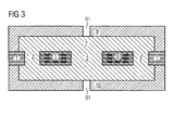
- the core consists of only one part 7 ( FIG. 3 ).
- the legs of the core are arranged in both embodiments in the openings 2, 3 and 4 of the ceramic multilayer body.
- the ferrite core can be built up from individual layers and then mechanically processed ( FIG. 2 ).
- casting of a ceramic slip or plastic deformation of a precisely sized ferrite mass is employed. This can also be done directly on the circuit carrier, as in FIG. 3 shown, done.
- the green-film composite is brought together with a sheath 9, 10, which has a sheath opening 91. Through the sheath opening ferrite mass is filled in as a slip or powder. After drying or pressure / heat treatment, the wrapper can be removed for later reuse. Subsequently, the sintering takes place, forming the ceramic multilayer body and the ferrite core.
Landscapes
- Engineering & Computer Science (AREA)
- Power Engineering (AREA)
- Manufacturing & Machinery (AREA)
- Microelectronics & Electronic Packaging (AREA)
- Coils Or Transformers For Communication (AREA)
- Soft Magnetic Materials (AREA)
Abstract
Description
- Die Erfindung betrifft ein monolithisches induktives Bauelement. Daneben werden ein Verfahren zum Herstellen des Bauelements und eine Verwendung des Bauelements angegeben.
- Ein Keramischer Mehrschichtkörper bietet hinsichtlich einer Miniaturisierung den Vorteil, dass in dessen Volumen elektrische Bauelemente, beispielsweise Leiterbahnen, Widerstände, Kapazitäten und Induktivitäten integriert werden können. Bekannte Herstellungsverfahren sind die HTCC(High Temperatur Cofired Ceramics)- und LTCC(Low Temperatur Cofired Ceramics)-Technologie. Bei diesen Technologie werden ungesinterte keramische Grünfolien unter Verwendung metallgefüllter, elektrisch leitfähiger Pasten in Stanz- und Siebdruckverfahren mit Durchkontaktierungen und planaren Leitungsstrukturen versehen und anschließend im Stapel zusammen gesintert. Dabei entstehen thermisch belastbare, hermetisch dichte, planare Mehrschicht-Substrate. Diese Mehrschicht-Substrate können als Schaltungsträger weiterer Bauelemente fungieren. Der Vorteil der LTCC-Technologie liegt darin, dass eine Dichtbrandtemperatur so niedrig ist, das bei relativ niedriger Temperatur schmelzende und elektrisch hochleitfähige Metalle wie Silber oder Kupfer zur Integration der Bauelemente verwendet werden können.
- Für viele Anwendungsgebiete, beispielsweise Strom- und Spannungstransformation oder Tiefpassfilter in leistungselektronischen Schaltungen, sind wegen der niedrigeren Frequenzen (im MHz-Bereich) induktive Bauelemente mit besserer magnetischer Kopplung auf Basis magnetischer Werkstoffe erforderlich, die den magnetischen Fluss verstärken und formen können. Hierfür sind zahlreiche Varianten von Spulen- und Transformatorkernen aus ferritischer Keramik verfügbar, die sich nachträglich mit Hilfe von Metallklammern an den erwähnten planaren Schaltungsträgern befestigen lassen.
- Die Integration solcher induktiver Bauelemente hat sich wegen divergierender Ansprüche an Material- und Prozesstechnik noch nicht etablieren können. Es treten vor allem zwei Probleme auf:
- Eine Steigerung der magnetischen Leistungsfähigkeit von Ferriten, d.h. eine Erhöhung der Permeabilität des Kernmaterials, mit Hilfe keramischer Technologien geht erfahrungsgemäß einher mit einer Abnahme des spezifischen Widerstandes des Kernmaterials und damit der Reduzierung der wichtigen Gleichspannungs-Isolation zwischen Primär- und Sekundärseite des Transformators.
- Sind Stromwicklungen homogen in Ferrit-Werkstoff eingebettet, so können sich magnetische Feldlinien teilweise auf kürzeren Wegen schließen ohne zur magnetischen Verkopplung der Windungen beizutragen; solche Streuinduktivitäten reduzieren die Leistungsfähigkeit des induktiven Bauelements.
- Beide Schwierigkeiten können grundsätzlich durch Einbettung der Strom führenden Windungen in gut isolierendes Material geringer Permeabilität gelöst werden. Eine derartige Lösung ist aus der
US 5,349,743 A bekannt. Darin ist ein Verfahren zum Herstellen eines monolithischen keramischen Mehrschichtkörpers mit integriertem Transformator bekannt. Dabei wird auf die LTCC-Technologie zurückgegriffen, wobei ein Werkstoff mit niedriger Permeabilität bei einem relativ hohen spezifischen elektrischen Widerstand und ein Werkstoff mit höherer Permeabilität bei einem relativ niedrigen spezifischen Widerstand verwendet werden. Die Integration dieser beiden Werkstoffe erfolgt durch Ausstanzen von Öffnungen in den Grünfolien des einen Werkstoffs, Füllen der Öffnungen mit Folienstücken oder Folienstapeln des anderen Werkstoffs und anschließendes gemeinsames Sintern. - Dieser Prozess, der im Grunde eine laterale Strukturierung von Grünfolien beinhaltet, ist aufwändig und relativ teuer.
- Aus der
US 5 655 287 A , welche als nächstliegender Stand der Technik angesehen wird, ist ein monolithisches Induktives Bauelement bekannt, sowie ein Herstellverfahren mit folgenden Schritten: - Bereitstellen eines Grünkörpers mit einem Grünfolienverbund zur Bildung eines keramischen Mehrschichtkörpers mit einer integrierten Wicklung und einem Formkörper aus ferritischen Kernmaterial,
- Wärmebehandeln des Grünkörpers, wobei aus dem Grünfolienverbund ein keramischer Mehrschichtkörper mit integrierter Wicklung und aus dem Formkörper ein magnetischer Kern mit dem ferritischen Kernmaterial entsteht.
- Aufgabe der Erfindung ist es daher, aufzuzeigen, wie ein induktives Bauelements in einem keramischen Mehrschichtkörper integriert werden kann.
- Zur Lösung der Aufgabe wird gemäß dem unabhängigen Anspruch 1 ein Verfahren zum Herstellen des monolithischen Bauelements mit folgenden Verfahrensschritten angegeben: a) Bereitstellen eines Grünkörpers mit einem Grünfolienverbund zur Bildung des keramischen Mehrschichtkörpers mit der integrierten Wicklung und einem Formkörper mit dem ferritischen Kernmaterial, b) Wärmebehandeln des Grünkörpers, wobei aus dem Grünfolienverbund der keramische Mehrschichtkörper mit integrierter Wicklung und aus dem Formkörper der magnetische Kern mit dem ferritischen Kernmaterial entsteht, dadurch gekennzeichnet, daß im Verfahrensschritt
a) der Grünfolienverbund mit einer Umhüllung Zusammengebracht wird, so dass ein Hohlraum mit einer Hohlraumöffnung zwischen der Umhüllung und dem Grünfolienverbund entsteht, und der Hohlraum durch die Hohlraumöffnung mit dem ferritischen Kernmaterial befüllt wird. - Der Grünkörper ist ein Grünfolienverbund. Der Formkörper ist ein Grünkörper mit frei geformtem ferritischen Kernmaterial. Grünfolienverbund und Formkörper bilden zusammen einen (gesamten) Grünkörper, der einem Cofiring-Prozess zugeführt wird.
- Der Formkörper mit dem ferritischen Keramikmaterial kann gemäß anderen beispielhaften Verfahren ein bereits verdichteter ferritischer Kern sein. Gemäß der Erfindung aber ist der Formkörper selbst ein Grünkörper. Dies bedeutet, dass bei der Wärmebehandlung ein Verdichten des ferritischen Keramikmaterials stattfindet. Unter Grünkörper ist allgemein ein keramischer Körper mit noch nicht verdichtetem Keramikmaterial. Der Grünkörper kann organische Additive wie Binder und Dispergator aufweisen. Der Grünkörper kann aber auch lediglich ein Pressling aus dem ferritischen Kernmaterial bzw. von Ausgangsstufen des ferritischen Kernmaterials bestehen. Aus den Ausgangsstufen bildet sich Kernmaterials bestehen. Aus den Ausgangsstufen bildet sich während der Wärmebehandlung das ferritische Keramikmaterial. Der Grünfolienverbund und der Formkörper werden in einem gemeinsamen Wärmebehandlungsschritt (Cofiring) zum monolithischen, also einstückigen induktiven Bauelement vereint.
- Im Hinblick auf die eingangs beschriebene Problematik ist es besonders vorteilhaft, die Wicklung im keramischen Mehrschichtkörper elektrisch zu isolieren. Daher weist gemäß einer besonderen Ausgestaltung der keramische Mehrschichtkörper dielektrisches Keramikmaterial auf.
- Zur Bildung eines effizienten induktiven Bauelements kann der Folienverbund Öffnungen aufweisen, in die das Formteil hineinragt. Beispielsweise ist eine derartige Öffnung von einer im Folienverbund mit Hilfe einer elektrisch leitfähigen Paste eingebrachten Wicklung umgeben.
- Das Formteil kann einteilig sein. Vorzugsweise ist das Formteil zwei- oder mehrteilig. Es besteht aus mindestens zwei Teilen. Dadurch kann eine effiziente Steuerung des magnetischen Flusses mit Hilfe des Kerns erzielt werden. So können durch Realisierung eines Luftspalts zwischen den Teilen des Kerns die auftretenden Streuinduktivitäten beeinflusst werden. Der Luftspalt kann dabei von einer dünnen keramischen Schicht des keramischen Mehrschichtkörpers mit niedriger Permittivität gebildet sein. Dazu wird beispielsweise die oben beschriebene Öffnung des Folienverbunds als Sackloch ausgestaltet, das durch Pastenoder Pulverprozessierung mit Segmenten des ferritischen Formteils gefüllt wird.
- Bei dem Verfahren werden die Funktionen der magnetischen Permeabilität und der elektrischen Isolation in ihren jeweiligen Raumgebieten des Bauelements durch jeweils maßgeschneiderte spezifische Keramiken verwirklicht, wodurch eine hohe Wirksamkeit des Designs und der Anforderung und Anwendung des Bauteils resultieren. Bedarfsabhängig können dabei unterschiedliche dielektrische und ferritische Keramikmaterialien verwendet werden. Soll das induktive Bauteil bei hohen Frequenzen, beispielsweise im Bereich zwischen 1 und 2 GHz verwendet werden, können bevorzugt Hexa-Ferrit-Keramiken, insbesondere Barium-Hexa-Ferrit-Keramiken verwendet werden. Diese weisen eine Permeabilität zwischen etwa 10 und 30 auf.
- Eine zweite Klasse von Keramiken kann dann verwendet werden, wenn Frequenzen im mittleren Bereich von etwa 10 bis etwa 30 MHz erforderlich sind. Dabei können beispielsweise CuNiZn-Ferrit-Materialien verwendet werden. Die Permeabilität von ferritischen Keramiken, die für Bauelemente zur Verwendung in diesem mittleren Frequenzbereich herangezogen werden, weisen Permeabilitätswerte von etwa 150 bis etwa 500 auf.
- Darüber hinaus ist eine weitere Klasse von Keramiken vorgesehen, die für Bauelemente im relativ niedrigen Frequenzbereich zwischen etwa 1 bis etwa 3 MHz verwendet werden. Dabei können beispielsweise MnZn-Ferrit-Materialien eingesetzt werden. Bevorzugt weisen Keramiken, welche in dieser Klasse eingesetzt werden, Permeabilitätswerte zwischen etwa 500 und 1000 auf.
- Die Erfindung kann in der HTCC-Technologie eingesetzt werden. Besonders vorteilhaft ist es aber, die Keramikmaterialien derart auszuwählen, dass eine Verdichtung bei relativ niedriger Temperatur stattfindet und damit die LTCC-Technolgie zum Einsatz kommen kann. In einer besonderen Ausgestaltung werden daher Grünfolien und/oder ein ferritisches Keramikmaterial mit Glas verwendet. Ein Glasanteil in einer Grünfolie bzw. im ferritischen Keramikmaterial sorgt für eine Verdichtung bei niedrigeren Temperaturen. Beim Sinterprozess entsteht eine Glaskeramik mit keramischer Phase und Glasphase. Das ferritische Keramikmaterial und/oder das dielektrische Keramikmaterial weisen Glas auf.
- Das Formteil kann gemäß anderen beispielhaften Verfahren vorgefertigt sein. Dies bedeutet, dass das Formteil vor dem Zusammenbringen mit dem Grünfolienverbund gefertigt wird. Gemäß der Erfindung wird aber das Formteil während des Zusammenbringens mit dem Grünfolienverbund hergestellt. Erfindungsgemäß wird daher zum Bereitstellen des Grünkörpers der Grünfolienverbund mit einer Umhüllung zusammengebracht, so dass ein Hohlraum mit einer Hohlraumöffnung zwischen der Umhüllung und dem Grünfolienverbund entsteht, und der Hohlraum durch die Hohlraumöffnung mit dem noch formbaren ferritischen Kernmaterial befüllt wird. Der Hohlraum wird beispielsweise mit dem oxidischen Ausgangsmaterial in Form eines Schüttgutes befüllt. Denkbar ist aber auch das Befüllen des Hohlraums mit einem Schlicker, der das ferritische Kernmaterial bzw. das Ausgangsmaterial des Kernmaterials enthält.
- Gemäß einer besonderen Ausgestaltung weist der Formkörper einen ferritischen Schlicker oder rieselfähiges ferritisches Grünpulver auf. Der Formkörper wird vor Entfernung der Umhüllung getrocknet bzw. unter Druck/Temperatur verdichtet.
- Die Umhüllung ist vorzugsweise elastisch verformbar. Dies bedeutet, dass von außen Druck auf das im Hohlraum eingefüllte, beispielsweise pulverförmige ferritische Kernmaterial ausgeübt werden kann, so dass eine stabile, selbsttragende Ferritform entsteht. Vorzugsweise wird dazu eine Umhüllung aus einem Silikon verwendet. Andere elastisch verformbare Umhüllungsmaterialien sind ebenfalls denkbar.
- Die Umhüllung kann zur Wärmebehandlung im Verbund mit dem Formteil und des Grünfolienverbund verbleiben. Vorzugsweise besteht die Umhüllung dazu aus einem organischen Material, das beim Wärmebehandeln aufoxidiert und über die Gasphase entfernt wird. Denkbar ist insbesondere aber auch, dass die Umhüllung nach dem Bilden des Formteils und vor dem Wärmebehandeln entfernt wird. Dazu kann die Umhüllung im Hohlraum einen Antihaftfilm aufweisen, der eine Trennung von Formteil und Umhüllung vereinfacht.
- Besonders vorteilhaft ist, dass das Verfahren im Nutzen durchgeführt werden kann. Es kann eine Vielzahl von Bauelementen parallel hergestellt werden.
- Die Ausgestaltung des induktiven Bauelements ist beliebig. Vorzugsweise weist das induktive Bauelement mindestens eine Spule und/oder mindestens einen Transformator auf.
- Verwendung findet das Bauelement in der Leistungselektronik, beispielsweise zur Strom- oder Spannungstransformation oder als Tiefpassfilter. Beispielsweise ist das Bauelement ein Schaltungselement eines elektronischen Vorschaltgeräts (EVG) für eine Entladungslampe.
- Zusammenfassend ergeben sich mit der Erfindung folgende besonderen Vorteile:
- Durch vollkeramische Bauweise erzielt das Bauelement eine hohe Temperaturverträglichkeit. Es ist dadurch für den Einbau in der Nähe von Wärmequellen, z.B. Lampen und Motoren geeignet.
- Niedrig sinterndes Ferritmaterial, z.B. spezielles MnZn-Ferrit, ermöglicht kostengünstige Fertigung im Nutzen in einem einzigen Sinterprozess zusammen mit dem keramischen Mehrschichtkörper (Platine).
- Durch monolithische Integration des Ferrits werden Temperaturdifferenzen zur Platine reduziert.
- Durch gezielten Einsatz des Ferrits allein am induktiven Bauelement wird eine kostengünstige Integrierbarkeit mit weiteren Schaltungskomponenten erreicht. Es sind keine ganzflächigen Ferrite wie bei einer einfachen, durchgängigen Folientechnik erforderlich.
- Mit der Erfindung kann ein Ferritvolumen minimiert werden. Durch das minimierte Ferritvolumen werden thermische Spannungen zwischen den verschiedenen Werkstoffen minimiert. Dies führt zu einer hohen Stabilität und sichereren Prozessführung.
- Die Ferritformteile können separat oder direkt auf dem Mehrschichtkörper in Hohlformen durch Verpressung von Grünpulver, durch Spritzguss oder ähnliche Verfahren hergestellt werden. Es ist somit nicht erforderlich, kleine Folienstücke zu handhaben.
- Eine Bauhöhe des Ferritkerns unterliegt geringeren Einschränkungen als beim Aufbau aus keramischen Grünfolien, so dass ein konstanter magnetischer Querschnitt ausreichender Größe entlang der gesamten magnetischen Weglänge erreicht und eine Überlastung des Ferritkerns vermieden werden.
- Die Funktionen der magnetischen Permeabilität und der elektrischen Isolation werden in ihren jeweiligen Raumgebieten durch jeweils maßgeschneiderte spezifische Keramiken verwirklicht, so dass hohe Wirksamkeit des Designs und hohe Performance des Bauteils resultieren.
- Anhand mehrer Ausführungsbeispiele und der dazugehörigen Figuren wird die Erfindung im Folgenden näher beschrieben. Die Figuren sind schematisch und stellen keine maßstabsgetreuen Abbildungen dar.
- Figuren 1 und 2
- zeigen jeweils ein monolithisches induktives Bauelement in einem seitlichen Querschnitt.
- Figur 3
- deutet ein Verfahren zum Herstellen eines monolithischen induktiven Bauelements an.
- Mit Hilfe der LTCC-Technologie wird ein monolithischer keramischer Mehrschichtkörper mit integriertem induktivem Bauelement hergestellt. Das induktive Bauelement ist ein Transformator. Die verwendeten keramischen Grünfolien weisen Glasanteile auf, so dass bei relativ niedriger Temperatur (unter 900° C) gesintert werden kann.
- Die ungesinterte Ferritmasse wird anschließend mit dem Grünfolienverbund zum gemeinsamen Sintern (Cofiring) verbunden.
- Die
Figuren 1 bis 3 zeigen jeweils einen planaren Transformators bzw. eine planare Spule in einem Schnitt senkrecht zum Schaltungsträger mit entsprechenden funktionellen Werkstoffen und Komponenten. - Das Bauelement besteht aus einem keramischen Mehrschichtkörper (mehrlagige Platine) 1 mit Öffnungen 2, 3 und 4. In den Bereichen 5 und 6 des Mehrschichtkörpers sind geschlossene, stromführende Windungen zwischen den Schichten eingebettet. Durch ein geeignetes Layout wird dabei beispielsweise erreicht, dass alle Ströme im Bereich 5 in die Bildebene hinein und im Bereich 6 aus ihr heraus fließen, so dass in der Öffnung 2 durch Überlagerung der Beiträge eine hohe magnetische Flussdichte zustande kommt.
- Der Transformator ist dabei durch zwei Spulen realisiert, die keine elektrisch leitende Verbindung untereinander besitzen, aber durch das Magnetfeld (induktiv) miteinander verkoppelt sind.
- Der Kern mit dem ferritischen Material besteht aus zwei Teilen 7 und 8 (
Figuren 1 und 2 ). Gemäß einer Alternativen Ausführungsform ist der Kern einstückig. Der Kern besteht nur aus einem einzigen Teil 7 (Figur 3 ). Die Schenkel des Kerns sind in beiden Ausführungsbeispielen in den Öffnungen 2, 3 und 4 des keramischen Mehrschichtkörpers angeordnet. - Zur Herstellung eines Formteils mit dem ferritischen Keramikmaterial werden unterschiedliche Formgebungsverfahren eingesetzt.
- Gemäß anderen beispielhaften Verfahren kann der Ferritkern aus einzelnen Lagen aufgebaut und dann mechanisch bearbeitet werden (
Figur 2 ). Alternativ dazu wird ein Gießen eines keramischen Schlickers oder die plastische Verformung einer genau bemessenen Ferritmasse eingesetzt. Dies kann z.B. auch direkt auf dem Schaltungsträger, wie inFigur 3 dargestellt, erfolgen. Dazu wird erfindungsgemäß der Grünfolienverbund mit einer Umhüllung 9, 10 zusammengebracht, die eine Umhüllungsöffnung 91 aufweist. Durch die Umhüllungsöffnung wird Ferritmasse als Schlicker oder Pulver eingefüllt. Nach Trocknung bzw. Druck/Wärmebehandlung kann die Umhüllung für spätere Wiederverwendung entfernt werden. Anschließend erfolgt die Sinterung, wobei sich der keramische Mehrschichtkörper und der Ferritkern bilden.
Claims (10)
- Verfahren zum Herstellen eines monolithischen induktiven Bauelements mit folgenden Verfahrensschritten:a) Bereitstellen eines Grünkörpers mit einem Grünfolienverbund zur Bildung eines keramischen Mehrschichtkörpers (1) mit einer integrierten Wicklung und einem Formkörper aus ferritischem Kernmaterial,b) Wärmebehandeln des Grünkörpers, wobei aus dem Grünfolienverbund ein keramischer Mehrschichtkörper (1) mit integrierter Wicklung und aus dem Formkörper ein magnetischer Kern (7) mit dem ferritischen Kernmaterial entsteht,dadurch gekennzeichnet, dass im Verfahrensschritt a) der Grünfolienverbund mit einer Umhüllung (9, 10) zusammengebracht wird, so dass ein Hohlraum mit einer Hohlraumöffnung (91) zwischen der Umhüllung und dem Grünfolienverbund entsteht, und der Hohlraum durch die Hohlraumöffnung mit dem ferritischen Kernmaterial befüllt wird.
- Verfahren nach Anspruch 1, wobei der Formkörper einen ferritischen Schlicker oder rieselfähiges ferritisches Grünpulver aufweist und der Formkörper vor Entfernung der Umhüllung getrocknet bzw. unter Druck/Temperatur verdichtet wird.
- Verfahren nach Anspruch 1 oder 2, wobei die Umhüllung vor dem Wärmebehandeln entfernt wird.
- Verfahren nach einem Ansprüche 1 bis 3, wobei eine Umhüllung aus einem Silikon verwendet wird.
- Verfahren nach Anspruch 3 oder 4, wobei die Umhüllung im Hohlraum mit einem Antihaftfilm versehen ist.
- Verfahren nach einem der Ansprüche 3 bis 5, wobei eine Vielzahl von induktiven monolithischen Bauelementen im Nutzen hergestellt wird.
- Verfahren nach einem der vorhergehenden Ansprüche, wobei der keramische Mehrschichtkörper (1) dielektrisches Keramikmaterial aufweist.
- Verfahren nach Anspruch 7, wobei der Formkörper zweiteilig ist.
- Verfahren nach einem der Ansprüche 7 oder 8, wobei das ferritische Kernmaterial und/oder das dielektrische Keramikmaterial Glas aufweisen.
- Verfahren nach einem der Ansprüche 7 bis 9, wobei das induktive Bauelement eine Induktionsspule und/oder einen Transformator aufweist.
Applications Claiming Priority (2)
| Application Number | Priority Date | Filing Date | Title |
|---|---|---|---|
| DE102007028239A DE102007028239A1 (de) | 2007-06-20 | 2007-06-20 | Monolithisches induktives Bauelement, Verfahren zum Herstellen des Bauelements und Verwendung des Bauelements |
| PCT/EP2008/057675 WO2008155344A1 (de) | 2007-06-20 | 2008-06-18 | Monolithisches induktives bauelement, verfahren zum herstellen des bauelements und verwendung des bauelements |
Publications (3)
| Publication Number | Publication Date |
|---|---|
| EP2158597A1 EP2158597A1 (de) | 2010-03-03 |
| EP2158597B1 true EP2158597B1 (de) | 2012-08-15 |
| EP2158597B8 EP2158597B8 (de) | 2012-09-26 |
Family
ID=39722492
Family Applications (1)
| Application Number | Title | Priority Date | Filing Date |
|---|---|---|---|
| EP08761143A Not-in-force EP2158597B8 (de) | 2007-06-20 | 2008-06-18 | Monolithisches induktives bauelement, verfahren zum herstellen des bauelements und verwendung des bauelements |
Country Status (6)
| Country | Link |
|---|---|
| US (1) | US8695208B2 (de) |
| EP (1) | EP2158597B8 (de) |
| KR (1) | KR101511058B1 (de) |
| CN (1) | CN101681714B (de) |
| DE (1) | DE102007028239A1 (de) |
| WO (1) | WO2008155344A1 (de) |
Families Citing this family (11)
| Publication number | Priority date | Publication date | Assignee | Title |
|---|---|---|---|---|
| JP5398676B2 (ja) * | 2009-09-24 | 2014-01-29 | 日本碍子株式会社 | コイル埋設型インダクタおよびその製造方法 |
| CN101789311A (zh) * | 2010-02-11 | 2010-07-28 | 深圳顺络电子股份有限公司 | 一种ltcc低温共烧陶瓷平面变压器 |
| CN101777413A (zh) * | 2010-02-11 | 2010-07-14 | 深圳顺络电子股份有限公司 | 一种ltcc低温共烧陶瓷功率电感器 |
| DE102011112826B4 (de) | 2011-05-23 | 2020-06-18 | Micro-Epsilon Messtechnik Gmbh & Co. Kg | Sensor und Verfahren zur Herstellung des Sensors |
| CN102683789B (zh) * | 2012-04-28 | 2015-11-18 | 深圳光启创新技术有限公司 | 一种谐振子及制备方法 |
| FR3009884B1 (fr) * | 2013-08-26 | 2016-12-09 | Centre Nat De La Rech Scient (C N R S) | Procede de fabrication d'un composant electromagnetique monolithique et composant magnetique monolithique associe |
| DE102016223039A1 (de) * | 2016-11-22 | 2018-05-24 | Audi Ag | Abschirmeinrichtung für eine am Unterboden eines Kraftfahrzeugs angeordnete Induktionsspule und damit ausgestattetes Kraftfahrzeug |
| CN108155888A (zh) * | 2018-01-05 | 2018-06-12 | 北京航天微电科技有限公司 | 一种用于抑制电源电磁干扰的ltcc大功率emi滤波器 |
| CN108807439B (zh) * | 2018-05-25 | 2020-09-25 | 复旦大学 | 一种基于高温共烧陶瓷的线阵图像传感器封装方法 |
| US11398334B2 (en) | 2018-07-30 | 2022-07-26 | At&S Austria Technologie & Systemtechnik Aktiengesellschaft | Component carrier comprising embedded inductor with an inlay |
| CN117238607B (zh) * | 2023-10-30 | 2025-04-29 | 北半球技术(苏州)有限公司 | 一种电感器及其制造方法 |
Family Cites Families (16)
| Publication number | Priority date | Publication date | Assignee | Title |
|---|---|---|---|---|
| DE69119557T2 (de) * | 1990-11-30 | 1996-10-17 | Intermetallics Co Ltd | Verfahren und Apparat zur Dauermagnet-Herstellung durch Formieren eines grünen und gesinterten Kompakts |
| US5087804A (en) * | 1990-12-28 | 1992-02-11 | Metcal, Inc. | Self-regulating heater with integral induction coil and method of manufacture thereof |
| US5349743A (en) | 1991-05-02 | 1994-09-27 | At&T Bell Laboratories | Method of making a multilayer monolithic magnet component |
| JPH0555044A (ja) * | 1991-08-23 | 1993-03-05 | Matsushita Electric Ind Co Ltd | インダクタンス部品およびその製造方法 |
| JP3099500B2 (ja) * | 1992-01-31 | 2000-10-16 | 株式会社村田製作所 | 複合積層トランス及びその製造方法 |
| JP3132786B2 (ja) * | 1992-08-19 | 2001-02-05 | 太陽誘電株式会社 | 積層チップインダクタおよびその製造方法 |
| JP3158757B2 (ja) * | 1993-01-13 | 2001-04-23 | 株式会社村田製作所 | チップ型コモンモードチョークコイル及びその製造方法 |
| TW265450B (en) * | 1994-06-30 | 1995-12-11 | At & T Corp | Devices using metallized magnetic substrates |
| US5945902A (en) * | 1997-09-22 | 1999-08-31 | Zefv Lipkes | Core and coil structure and method of making the same |
| JPH11171645A (ja) * | 1997-12-09 | 1999-06-29 | Hitachi Metals Ltd | 電子部品 |
| CN1141722C (zh) * | 1998-08-10 | 2004-03-10 | 广东肇庆风华电子工程开发有限公司 | 高性能低温烧结多层片式电感器制作工艺 |
| JP3449350B2 (ja) * | 2000-11-09 | 2003-09-22 | 株式会社村田製作所 | 積層セラミック電子部品の製造方法及び積層セラミック電子部品 |
| JP3685720B2 (ja) * | 2001-02-16 | 2005-08-24 | 三洋電機株式会社 | 積層型複合デバイス及びその製造方法 |
| EP1367611A4 (de) * | 2001-03-08 | 2010-01-13 | Panasonic Corp | Induktivitätsbauelement und verfahren zu seiner herstellung |
| JP2004200227A (ja) * | 2002-12-16 | 2004-07-15 | Alps Electric Co Ltd | プリントインダクタ |
| JP5204403B2 (ja) * | 2003-09-04 | 2013-06-05 | コーニンクレッカ フィリップス エレクトロニクス エヌ ヴィ | フェライト高分子コアを有する端数巻き変圧器 |
-
2007
- 2007-06-20 DE DE102007028239A patent/DE102007028239A1/de not_active Ceased
-
2008
- 2008-06-18 WO PCT/EP2008/057675 patent/WO2008155344A1/de not_active Ceased
- 2008-06-18 EP EP08761143A patent/EP2158597B8/de not_active Not-in-force
- 2008-06-18 KR KR1020107001342A patent/KR101511058B1/ko not_active Expired - Fee Related
- 2008-06-18 US US12/602,799 patent/US8695208B2/en not_active Expired - Fee Related
- 2008-06-18 CN CN200880021235.1A patent/CN101681714B/zh not_active Expired - Fee Related
Also Published As
| Publication number | Publication date |
|---|---|
| KR101511058B1 (ko) | 2015-04-10 |
| US8695208B2 (en) | 2014-04-15 |
| EP2158597A1 (de) | 2010-03-03 |
| CN101681714B (zh) | 2012-08-22 |
| CN101681714A (zh) | 2010-03-24 |
| WO2008155344A1 (de) | 2008-12-24 |
| US20100171582A1 (en) | 2010-07-08 |
| DE102007028239A1 (de) | 2009-01-02 |
| EP2158597B8 (de) | 2012-09-26 |
| KR20100042627A (ko) | 2010-04-26 |
Similar Documents
| Publication | Publication Date | Title |
|---|---|---|
| EP2158597B1 (de) | Monolithisches induktives bauelement, verfahren zum herstellen des bauelements und verwendung des bauelements | |
| EP2018643B1 (de) | Induktives bauelement und verfahren zum herstellen eines induktiven bauelements | |
| DE69231827T2 (de) | Verfahren zur Herstellung von magnetischer Vielschicht-Komponenten | |
| US6459351B1 (en) | Multilayer component having inductive impedance | |
| DE69332599T2 (de) | Bei niedriger Temperatur gesinterte keramische Bandstruktur mit gleichzeitig gesintertem ferromagnetischen Element | |
| JP4969242B2 (ja) | 内蔵トロイダルインダクタ | |
| KR101994722B1 (ko) | 적층형 전자부품 | |
| US6504466B1 (en) | Lamination-type coil component and method of producing the same | |
| DE19838587B4 (de) | Induktivität und Verfahren zum Herstellen eines Induktivität | |
| DE102009046183A1 (de) | Vorrichtung mit einem magnetischen Bauelement und Verfahren zu dessen Herstellung | |
| EP3547338A1 (de) | Elektronisches bauelement und verfahren zu dessen herstellung | |
| EP2401897B1 (de) | Mehrlagiger schaltungsträger und verfahren zu dessen herstellung | |
| WO2018095757A1 (de) | Transformatorvorrichtung, transformator und verfahren zur herstellung einer transformatorvorrichtung | |
| DE102008034691A1 (de) | Keramischer Mehrschichtkörper, Induktives Bauelement mit dem Mehrschichtkörper und Verfahren zum Herstellen des Mehrschichtkörpers | |
| DE19639881C2 (de) | Verfahren zum Herstellen eines induktiven Bauelements | |
| DE4312455A1 (de) | Nicht-reziprokes Schaltungselement | |
| DE3628021A1 (de) | Chip-bauteil mit wenigstens einer spule und verfahren zu dessen herstellung | |
| DE102007028240B3 (de) | Verfahren zum Herstellen eines keramischen Mehrschichtkörpers mit lateral strukturierter Keramiklage | |
| JP2921594B2 (ja) | 積層チップ・インダクタの製造方法 | |
| WO2017162376A1 (de) | Verfahren zur herstellung eines ableiters und ableiter | |
| JP2983049B2 (ja) | 積層チップ・インダクタの製造方法 | |
| JPH08330137A (ja) | 積層インダクタ | |
| JPH0818376A (ja) | 分布定数型ノイズフィルタ | |
| KR100649681B1 (ko) | 비어홀로서 금속체가 삽입된 칩부품과 그 제조방법 | |
| JPH0660134U (ja) | 積層チップemi除去フィルタ |
Legal Events
| Date | Code | Title | Description |
|---|---|---|---|
| PUAI | Public reference made under article 153(3) epc to a published international application that has entered the european phase |
Free format text: ORIGINAL CODE: 0009012 |
|
| 17P | Request for examination filed |
Effective date: 20090929 |
|
| AK | Designated contracting states |
Kind code of ref document: A1 Designated state(s): AT BE BG CH CY CZ DE DK EE ES FI FR GB GR HR HU IE IS IT LI LT LU LV MC MT NL NO PL PT RO SE SI SK TR |
|
| AX | Request for extension of the european patent |
Extension state: AL BA MK RS |
|
| DAX | Request for extension of the european patent (deleted) | ||
| 17Q | First examination report despatched |
Effective date: 20111007 |
|
| GRAP | Despatch of communication of intention to grant a patent |
Free format text: ORIGINAL CODE: EPIDOSNIGR1 |
|
| RAP1 | Party data changed (applicant data changed or rights of an application transferred) |
Owner name: OSRAM AG |
|
| GRAS | Grant fee paid |
Free format text: ORIGINAL CODE: EPIDOSNIGR3 |
|
| GRAA | (expected) grant |
Free format text: ORIGINAL CODE: 0009210 |
|
| AK | Designated contracting states |
Kind code of ref document: B1 Designated state(s): AT BE BG CH CY CZ DE DK EE ES FI FR GB GR HR HU IE IS IT LI LT LU LV MC MT NL NO PL PT RO SE SI SK TR |
|
| REG | Reference to a national code |
Ref country code: AT Ref legal event code: REF Ref document number: 571200 Country of ref document: AT Kind code of ref document: T Effective date: 20120815 Ref country code: GB Ref legal event code: FG4D Free format text: NOT ENGLISH Ref country code: CH Ref legal event code: EP |
|
| REG | Reference to a national code |
Ref country code: IE Ref legal event code: FG4D Free format text: LANGUAGE OF EP DOCUMENT: GERMAN |
|
| RAP2 | Party data changed (patent owner data changed or rights of a patent transferred) |
Owner name: SIEMENS AKTIENGESELLSCHAFT |
|
| REG | Reference to a national code |
Ref country code: DE Ref legal event code: R096 Ref document number: 502008007966 Country of ref document: DE Effective date: 20121011 |
|
| REG | Reference to a national code |
Ref country code: DE Ref legal event code: R081 Ref document number: 502008007966 Country of ref document: DE Owner name: SIEMENS AKTIENGESELLSCHAFT, DE Free format text: FORMER OWNER: OSRAM AG, 81543 MUENCHEN, DE Effective date: 20121015 |
|
| REG | Reference to a national code |
Ref country code: NL Ref legal event code: VDEP Effective date: 20120815 |
|
| PG25 | Lapsed in a contracting state [announced via postgrant information from national office to epo] |
Ref country code: FI Free format text: LAPSE BECAUSE OF FAILURE TO SUBMIT A TRANSLATION OF THE DESCRIPTION OR TO PAY THE FEE WITHIN THE PRESCRIBED TIME-LIMIT Effective date: 20120815 Ref country code: HR Free format text: LAPSE BECAUSE OF FAILURE TO SUBMIT A TRANSLATION OF THE DESCRIPTION OR TO PAY THE FEE WITHIN THE PRESCRIBED TIME-LIMIT Effective date: 20120815 Ref country code: CY Free format text: LAPSE BECAUSE OF FAILURE TO SUBMIT A TRANSLATION OF THE DESCRIPTION OR TO PAY THE FEE WITHIN THE PRESCRIBED TIME-LIMIT Effective date: 20120815 Ref country code: NO Free format text: LAPSE BECAUSE OF FAILURE TO SUBMIT A TRANSLATION OF THE DESCRIPTION OR TO PAY THE FEE WITHIN THE PRESCRIBED TIME-LIMIT Effective date: 20121115 Ref country code: LT Free format text: LAPSE BECAUSE OF FAILURE TO SUBMIT A TRANSLATION OF THE DESCRIPTION OR TO PAY THE FEE WITHIN THE PRESCRIBED TIME-LIMIT Effective date: 20120815 Ref country code: IS Free format text: LAPSE BECAUSE OF FAILURE TO SUBMIT A TRANSLATION OF THE DESCRIPTION OR TO PAY THE FEE WITHIN THE PRESCRIBED TIME-LIMIT Effective date: 20121215 |
|
| PG25 | Lapsed in a contracting state [announced via postgrant information from national office to epo] |
Ref country code: PL Free format text: LAPSE BECAUSE OF FAILURE TO SUBMIT A TRANSLATION OF THE DESCRIPTION OR TO PAY THE FEE WITHIN THE PRESCRIBED TIME-LIMIT Effective date: 20120815 Ref country code: PT Free format text: LAPSE BECAUSE OF FAILURE TO SUBMIT A TRANSLATION OF THE DESCRIPTION OR TO PAY THE FEE WITHIN THE PRESCRIBED TIME-LIMIT Effective date: 20121217 Ref country code: SE Free format text: LAPSE BECAUSE OF FAILURE TO SUBMIT A TRANSLATION OF THE DESCRIPTION OR TO PAY THE FEE WITHIN THE PRESCRIBED TIME-LIMIT Effective date: 20120815 Ref country code: LV Free format text: LAPSE BECAUSE OF FAILURE TO SUBMIT A TRANSLATION OF THE DESCRIPTION OR TO PAY THE FEE WITHIN THE PRESCRIBED TIME-LIMIT Effective date: 20120815 Ref country code: SI Free format text: LAPSE BECAUSE OF FAILURE TO SUBMIT A TRANSLATION OF THE DESCRIPTION OR TO PAY THE FEE WITHIN THE PRESCRIBED TIME-LIMIT Effective date: 20120815 Ref country code: GR Free format text: LAPSE BECAUSE OF FAILURE TO SUBMIT A TRANSLATION OF THE DESCRIPTION OR TO PAY THE FEE WITHIN THE PRESCRIBED TIME-LIMIT Effective date: 20121116 |
|
| RAP2 | Party data changed (patent owner data changed or rights of a patent transferred) |
Owner name: SIEMENS AKTIENGESELLSCHAFT |
|
| PG25 | Lapsed in a contracting state [announced via postgrant information from national office to epo] |
Ref country code: NL Free format text: LAPSE BECAUSE OF FAILURE TO SUBMIT A TRANSLATION OF THE DESCRIPTION OR TO PAY THE FEE WITHIN THE PRESCRIBED TIME-LIMIT Effective date: 20120815 |
|
| PG25 | Lapsed in a contracting state [announced via postgrant information from national office to epo] |
Ref country code: CZ Free format text: LAPSE BECAUSE OF FAILURE TO SUBMIT A TRANSLATION OF THE DESCRIPTION OR TO PAY THE FEE WITHIN THE PRESCRIBED TIME-LIMIT Effective date: 20120815 Ref country code: ES Free format text: LAPSE BECAUSE OF FAILURE TO SUBMIT A TRANSLATION OF THE DESCRIPTION OR TO PAY THE FEE WITHIN THE PRESCRIBED TIME-LIMIT Effective date: 20121126 Ref country code: EE Free format text: LAPSE BECAUSE OF FAILURE TO SUBMIT A TRANSLATION OF THE DESCRIPTION OR TO PAY THE FEE WITHIN THE PRESCRIBED TIME-LIMIT Effective date: 20120815 Ref country code: DK Free format text: LAPSE BECAUSE OF FAILURE TO SUBMIT A TRANSLATION OF THE DESCRIPTION OR TO PAY THE FEE WITHIN THE PRESCRIBED TIME-LIMIT Effective date: 20120815 Ref country code: RO Free format text: LAPSE BECAUSE OF FAILURE TO SUBMIT A TRANSLATION OF THE DESCRIPTION OR TO PAY THE FEE WITHIN THE PRESCRIBED TIME-LIMIT Effective date: 20120815 |
|
| PG25 | Lapsed in a contracting state [announced via postgrant information from national office to epo] |
Ref country code: SK Free format text: LAPSE BECAUSE OF FAILURE TO SUBMIT A TRANSLATION OF THE DESCRIPTION OR TO PAY THE FEE WITHIN THE PRESCRIBED TIME-LIMIT Effective date: 20120815 Ref country code: IT Free format text: LAPSE BECAUSE OF FAILURE TO SUBMIT A TRANSLATION OF THE DESCRIPTION OR TO PAY THE FEE WITHIN THE PRESCRIBED TIME-LIMIT Effective date: 20120815 |
|
| PLBE | No opposition filed within time limit |
Free format text: ORIGINAL CODE: 0009261 |
|
| STAA | Information on the status of an ep patent application or granted ep patent |
Free format text: STATUS: NO OPPOSITION FILED WITHIN TIME LIMIT |
|
| 26N | No opposition filed |
Effective date: 20130516 |
|
| PG25 | Lapsed in a contracting state [announced via postgrant information from national office to epo] |
Ref country code: BG Free format text: LAPSE BECAUSE OF FAILURE TO SUBMIT A TRANSLATION OF THE DESCRIPTION OR TO PAY THE FEE WITHIN THE PRESCRIBED TIME-LIMIT Effective date: 20121115 |
|
| REG | Reference to a national code |
Ref country code: DE Ref legal event code: R097 Ref document number: 502008007966 Country of ref document: DE Effective date: 20130516 |
|
| BERE | Be: lapsed |
Owner name: OSRAM A.G. Effective date: 20130630 |
|
| PG25 | Lapsed in a contracting state [announced via postgrant information from national office to epo] |
Ref country code: MC Free format text: LAPSE BECAUSE OF FAILURE TO SUBMIT A TRANSLATION OF THE DESCRIPTION OR TO PAY THE FEE WITHIN THE PRESCRIBED TIME-LIMIT Effective date: 20120815 |
|
| REG | Reference to a national code |
Ref country code: CH Ref legal event code: PL |
|
| REG | Reference to a national code |
Ref country code: IE Ref legal event code: MM4A |
|
| PG25 | Lapsed in a contracting state [announced via postgrant information from national office to epo] |
Ref country code: BE Free format text: LAPSE BECAUSE OF NON-PAYMENT OF DUE FEES Effective date: 20130630 |
|
| PG25 | Lapsed in a contracting state [announced via postgrant information from national office to epo] |
Ref country code: LI Free format text: LAPSE BECAUSE OF NON-PAYMENT OF DUE FEES Effective date: 20130630 Ref country code: IE Free format text: LAPSE BECAUSE OF NON-PAYMENT OF DUE FEES Effective date: 20130618 Ref country code: CH Free format text: LAPSE BECAUSE OF NON-PAYMENT OF DUE FEES Effective date: 20130630 |
|
| REG | Reference to a national code |
Ref country code: AT Ref legal event code: MM01 Ref document number: 571200 Country of ref document: AT Kind code of ref document: T Effective date: 20130618 |
|
| PG25 | Lapsed in a contracting state [announced via postgrant information from national office to epo] |
Ref country code: AT Free format text: LAPSE BECAUSE OF NON-PAYMENT OF DUE FEES Effective date: 20130618 |
|
| PG25 | Lapsed in a contracting state [announced via postgrant information from national office to epo] |
Ref country code: MT Free format text: LAPSE BECAUSE OF FAILURE TO SUBMIT A TRANSLATION OF THE DESCRIPTION OR TO PAY THE FEE WITHIN THE PRESCRIBED TIME-LIMIT Effective date: 20120815 |
|
| REG | Reference to a national code |
Ref country code: FR Ref legal event code: PLFP Year of fee payment: 8 |
|
| PG25 | Lapsed in a contracting state [announced via postgrant information from national office to epo] |
Ref country code: TR Free format text: LAPSE BECAUSE OF FAILURE TO SUBMIT A TRANSLATION OF THE DESCRIPTION OR TO PAY THE FEE WITHIN THE PRESCRIBED TIME-LIMIT Effective date: 20120815 |
|
| PG25 | Lapsed in a contracting state [announced via postgrant information from national office to epo] |
Ref country code: HU Free format text: LAPSE BECAUSE OF FAILURE TO SUBMIT A TRANSLATION OF THE DESCRIPTION OR TO PAY THE FEE WITHIN THE PRESCRIBED TIME-LIMIT; INVALID AB INITIO Effective date: 20080618 Ref country code: LU Free format text: LAPSE BECAUSE OF NON-PAYMENT OF DUE FEES Effective date: 20130618 |
|
| PGFP | Annual fee paid to national office [announced via postgrant information from national office to epo] |
Ref country code: GB Payment date: 20150608 Year of fee payment: 8 |
|
| PGFP | Annual fee paid to national office [announced via postgrant information from national office to epo] |
Ref country code: FR Payment date: 20150610 Year of fee payment: 8 |
|
| PGFP | Annual fee paid to national office [announced via postgrant information from national office to epo] |
Ref country code: DE Payment date: 20150821 Year of fee payment: 8 |
|
| REG | Reference to a national code |
Ref country code: DE Ref legal event code: R119 Ref document number: 502008007966 Country of ref document: DE |
|
| GBPC | Gb: european patent ceased through non-payment of renewal fee |
Effective date: 20160618 |
|
| REG | Reference to a national code |
Ref country code: FR Ref legal event code: ST Effective date: 20170228 |
|
| PG25 | Lapsed in a contracting state [announced via postgrant information from national office to epo] |
Ref country code: DE Free format text: LAPSE BECAUSE OF NON-PAYMENT OF DUE FEES Effective date: 20170103 Ref country code: FR Free format text: LAPSE BECAUSE OF NON-PAYMENT OF DUE FEES Effective date: 20160630 |
|
| PG25 | Lapsed in a contracting state [announced via postgrant information from national office to epo] |
Ref country code: GB Free format text: LAPSE BECAUSE OF NON-PAYMENT OF DUE FEES Effective date: 20160618 |