EP2219240A2 - Lichtemittierendes Halbleiterbauelement - Google Patents
Lichtemittierendes Halbleiterbauelement Download PDFInfo
- Publication number
- EP2219240A2 EP2219240A2 EP10153590A EP10153590A EP2219240A2 EP 2219240 A2 EP2219240 A2 EP 2219240A2 EP 10153590 A EP10153590 A EP 10153590A EP 10153590 A EP10153590 A EP 10153590A EP 2219240 A2 EP2219240 A2 EP 2219240A2
- Authority
- EP
- European Patent Office
- Prior art keywords
- layer
- light emitting
- emitting device
- semiconductor light
- isolation
- Prior art date
- Legal status (The legal status is an assumption and is not a legal conclusion. Google has not performed a legal analysis and makes no representation as to the accuracy of the status listed.)
- Granted
Links
Images


Classifications
-
- H—ELECTRICITY
- H10—SEMICONDUCTOR DEVICES; ELECTRIC SOLID-STATE DEVICES NOT OTHERWISE PROVIDED FOR
- H10H—INORGANIC LIGHT-EMITTING SEMICONDUCTOR DEVICES HAVING POTENTIAL BARRIERS
- H10H20/00—Individual inorganic light-emitting semiconductor devices having potential barriers, e.g. light-emitting diodes [LED]
- H10H20/80—Constructional details
- H10H20/84—Coatings, e.g. passivation layers or antireflective coatings
- H10H20/841—Reflective coatings, e.g. dielectric Bragg reflectors
-
- H—ELECTRICITY
- H10—SEMICONDUCTOR DEVICES; ELECTRIC SOLID-STATE DEVICES NOT OTHERWISE PROVIDED FOR
- H10H—INORGANIC LIGHT-EMITTING SEMICONDUCTOR DEVICES HAVING POTENTIAL BARRIERS
- H10H20/00—Individual inorganic light-emitting semiconductor devices having potential barriers, e.g. light-emitting diodes [LED]
- H10H20/01—Manufacture or treatment
- H10H20/011—Manufacture or treatment of bodies, e.g. forming semiconductor layers
- H10H20/018—Bonding of wafers
Definitions
- the embodiment relates to a semiconductor light emitting device and a method of manufacturing the same.
- Group III-V nitride semiconductors are spotlighted as core materials of light emitting diodes (LEDs) or laser diodes (LDs) due to physical and chemical characteristics.
- the group III-V nitride semiconductors include semiconductor materials having a composition formula of In x Al y Ga 1-x-y N (0 ⁇ x ⁇ 1, 0 ⁇ y ⁇ 1, 0 ⁇ x+y ⁇ 1).
- the LED is a kind of a semiconductor device, which transmits signals by converting electricity into light using the characteristic of a compound semiconductor and is used as a light source.
- the LED and LD employing such nitride semiconductors have been mainly used in light emitting devices to obtain light, and have been applied to various appliances (e.g., a light emitting part of a key pad of a portable phone, an electric bulletin board, an illumination device) as a light source.
- various appliances e.g., a light emitting part of a key pad of a portable phone, an electric bulletin board, an illumination device
- the embodiment provides a semiconductor light emitting device and a method of manufacturing the same, capable of preventing the loss of light efficiency from a lateral side of a light emitting structure.
- the embodiment relates to a semiconductor light emitting device and a method of manufacturing the same, capable of preventing delamination and breaking by interposing a metal layer between isolation layers.
- the semiconductor light emitting device includes a light emitting structure including a first conductive semiconductor layer, an active layer, and a second conductive semiconductor layer, a plurality of isolation layers formed along an outer peripheral portion of the light emitting structure below the light emitting structure, a metal layer interposed between the isolation layers, and a second electrode layer formed below the light emitting structure.
- the semiconductor light emitting device includes a light emitting structure including a first conductive semiconductor layer, an active layer, and a second conductive semiconductor layer, a first isolation layer disposed along an outer peripheral portion of the light emitting structure below the light emitting structure, a metal layer disposed below the first isolation layer, a second isolation layer disposed below the metal layer, and a second electrode layer disposed below the second conductive semiconductor layer.
- a method of manufacturing the semiconductor light emitting device is as follows.
- a light emitting structure including a first conductive semiconductor layer, an active layer, and a second conductive semiconductor layer is formed.
- a first isolation layer is formed along an outer peripheral portion of the light emitting structure.
- a metal layer is formed on the first isolation layer.
- a second isolation layer is formed on the metal layer.
- a second electrode layer is formed on the light emitting structure and the second isolation layer.
- an adhesive strength can be improved between a light emitting structure and another layer.
- light extraction efficiency of the semiconductor light emitting device can be improved, and delamination can be prevented.
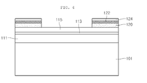
- FIG. 1 is a view showing a semiconductor light emitting device 100 according to the embodiment.
- the semiconductor light emitting device 100 includes a light emitting structure 110, a first electrode layer 119, a first isolation layer 120, a metal layer 122, a second isolation layer 124, a second electrode layer 130, and a conductive support member 140.
- the light emitting structure 110 includes a first conductive semiconductor layer 111, an active layer 113, and a second conductive semiconductor layer 115.
- the active layer 113 is interposed between the first and second conductive semiconductor layers 111 and 115.
- the first conductive semiconductor layer 111 may be realized by using at least one semiconductor layer doped with first conductive dopants.
- the first conductive semiconductor layer 111 may be realized by using a group III-V compound semiconductor.
- the first conductive semiconductor layer 111 may be formed of at least one of GaN, InN, AlN, InGaN, AlGaN, InAlGaN, and AlInN.
- the first conductive semiconductor layer 111 is an N-type semiconductor layer
- the first conductive dopant may be an N-type dopant.
- the N-type dopant may be selected from among V-group elements.
- the first conductive semiconductor layer 111 may be disposed thereon with the first electrode layer 119 having a predetermined pattern.
- concave-convex shape roughness may be formed on a portion of a top surface of the first conductive semiconductor layer 111 or the entire portion of the top surface of the first conductive semiconductor layer 111.
- the active layer 113 is disposed below the first conductive semiconductor layer 111.
- the active layer 113 may have a single quantum well (SQW) structure or a multiple quantum well (MQW) structure.
- the active layer 113 may be formed at a cycle of a well layer and a barrier layer by using group III-V compound semiconductor materials.
- the active layer 113 may be formed at a cycle of an InGaN well layer/GaN barrier layer or an AlGaN well layer/GaN barrier layer.
- the active layer 113 includes a material having a band-gap energy corresponding to the wavelength of light to be emitted. For example, if blue light having a wavelength in the range of 460 nm to 470 nm is emitted, the active layer 113 may be formed in the SQW structure or the MQW structure at a cycle of the InGaN well layer/GaN barrier layer. For example, the active layer 113 may be realized to emit light in a visible ray region having blue, red, and green wavelengths. In addition, the active layer 113 may be realized to emit light in an ultraviolet ray region.
- a conductive clad layer may be disposed above and/or below the active layer 113.
- the conductive clad layer may include an AlGaN layer.
- the second conductive semiconductor layer 115 may be disposed below the active layer 113.
- the second conductive semiconductor layer 115 may be realized by using at least one semiconductor layer doped with second conductive dopants.
- the second conductive semiconductor layer 115 may be realized by using a group III-V compound semiconductor.
- the second conductive semiconductor layer 115 may be formed of at least one of GaN, InN, AlN, InGaN, AlGaN, InAlGaN, and AlInN.
- the second conductive semiconductor layer 115 is a P-type semiconductor layer
- the second conductive dopant may be a P-type dopant.
- the P-type dopant may be selected from among group III elements.
- a third conductive semiconductor layer may be additionally disposed below the second conductive semiconductor layer 115. If the conductive semiconductor layer 111 is a P-type semiconductor layer, the second conductive semiconductor layer 115 may be realized as an N-type semiconductor layer. The third conductive semiconductor layer may be realized as a semiconductor layer doped with P-type dopants.
- the light emitting structure 110 may include one of an N-P junction structure, a P-N junction structure, an N-P-N junction structure, and a P-N-P junction structure.
- the first isolation layer 120 and the second electrode layer 130 are disposed below the second conductive semiconductor layer 115.
- An inner portion of the first isolation layer 120 is formed along an outer peripheral portion of the second conductive semiconductor layer 115 below the second conductive semiconductor layer 115.
- An outer portion of the first isolation layer 120 extends outward below the second conductive semiconductor layer 115 and is exposed along an outer region 118 of the light emitting structure 110.
- the first isolation layer 120 may be formed in the form of a frame by using a conductive transmissive material having light transmittance or an insulating material.
- the first isolation layer 120 is formed along a lower portion of the second conductive semiconductor layer 115.
- the first isolation layer 120 may be formed of a conductive transmissive material such as ITO, IZO, IZTO, IAZO, IGZO, IGTO, AZO, or ATO.
- the first isolation layer 120 may include a metal oxide such as a transparent conductive oxide (TCO).
- the first isolation layer 120 includes a conductive transmissive material, the first isolation layer 120 transmits a laser beam irradiated in a mesa etching process. Accordingly, when the laser beam is irradiated, an outer portion of the light emitting structure 110 is not damaged, so that light emitting efficiency can be improved.
- the first isolation layer 120 may be formed of an insulating material such as SiO 2 , SiO x , SiO x N y , Si 3 N 4 , Al 2 O 3 , or TiO 2 . According to the embodiment, the first isolation layer 120 spaces the conductive support member 140 apart from the light emitting structure 110. The first isolation layer 120 can increase the adhesive strength with the second conductive semiconductor layer 115.
- the metal layer 122 may be formed below the first isolation layer 120.
- the metal layer 122 may be formed of at least one layer made of metal having a high reflective index, in which the metal may be selected from the group consisting of Ag, Ni, Al, Rh, Pd, Ir, Ru, Mg, Zn, Pt, Au, Hf, and the combination thereof.
- the second isolation layer 124 may be disposed below the metal layer 122.
- the second isolation layer 124 may be formed of at least one selected from the group consisting of ITO, IZO, IZTO, IAZO, IGZO, IGTO, AZO, ATO, SiO 2 , SiO x , SiO x N y , Si 3 N 4 , Al 2 O 3 , TiO 2 .
- the first isolation layer 120 and the second isolation layer 124 may include the same material or different materials.
- the first isolation layer 120 may be thicker than the second isolation layer 124.
- the first isolation layer 120 may be thicker than the second electrode layer 130.
- the first isolation layer 120, the metal layer 122, the second isolation layer 124, and the second electrode layer 130 may have various thicknesses and the relative thickness thereof may be changed.
- the second isolation layer 124 may be thicker than the first isolation layer 120.
- the first isolation layer 120, the metal layer 122, and the second isolation layer 124 may be formed in-situ by using one equipment.
- the metal layer 122 is interposed between the first and second isolation layers 120 and 124, so that an inter-layer adhesive strength can be improved, thereby preventing delamination.
- the second electrode layer 130 may be disposed below the light emitting structure 110.
- the second electrode layer 130 may be disposed below an inner portion of the light emitting structure 110.
- the second electrode layer 130 may be formed of at least one layer made of at least one selected from the group consisting of Ag, Ni, Al, Rh, Pd, Ir, Ru, Mg, Zn, Pt, Au, Hf, and the combination thereof.
- the second electrode layer 130 is not integrated with the metal layer 122, the second electrode layer 130 and the metal layer 122 can be prevented from interfering with each other due to thermal expansion.
- An ohmic layer (not shown) having a predetermined pattern may be formed between the second electrode layer 130 and the second conductive semiconductor layer 115.
- the pattern of the ohmic layer may have the shape of a matrix, a cross, a polygon, or a circle.
- the ohmic layer may be formed of ITO, IZO, IZTO, IAZO, IGZO, IGTO, AZO, or ATO.
- the ohmic layer may include a conductive oxide or metal.
- the ohmic layer may be realized in a single layer structure or a multiple layer structure by using at least one of ITO, IZO, IZTO, IAZO, IGZO, IGTO, AZO, ATO, GZO, IrOx, RuOx, RuOx/ITO, Ni, Ag, Ni/IrOx/Au, and Ni/IrOx/Au/ITO.
- the conductive support member 140 may be disposed below the second electrode layer 130.
- the conductive support member 140 is a base substrate.
- the conductive support member 140 may be realized by using Cu, Au, Ni, Mo, Cu-W, or a carrier wafer including a material such as Si, Ge, GaA, ZnO, SiC, GaN, SiGe, or Ga 2 O 3 .
- the conductive support member 140 may be realized by using a conductive sheet.
- the conductive support member 140 may be bonded or prepared as a plated layer. In addition, the conductive support member 140 may be attached as a conductive sheet.
- FIGS. 2 to 9 are sectional views showing the manufacturing process of the semiconductor light emitting device according to the embodiment.
- the first conductive semiconductor layer 111 is formed on a substrate 101.
- the active layer 113 is formed on the first conductive semiconductor layer 111, and the second conductive semiconductor layer 115 is formed on the active layer 113.
- the substrate 101 may include one selected from the group consisting of Al 2 0 3 , GaN, SiC, ZnO, Si, GaP, InP, and GaAs.
- a predetermined concave-convex pattern may be formed on the substrate 101.
- the substrate 101 may be disposed thereon with another semiconductor layer such as a buffer layer and/or an undoped semiconductor layer, but the embodiment is not limited thereto.
- the first semiconductor layer 111 may be realized as an N-type semiconductor layer.
- the second semiconductor layer 115 may be realized as a P-type semiconductor layer.
- the first semiconductor layer 111 may be realized as a P-type semiconductor layer and the second semiconductor layer 115 may be realized as an N-type semiconductor layer.
- An additional semiconductor layer such as a buffer layer and/or an undoped semiconductor layer may be formed between the substrate 101 and the first conductive semiconductor layer 111. After thin film growth, the additional layer may be separated or removed from the structure.
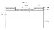
- the first isolation layer 120 is formed on an outer peripheral portion of the second conductive semiconductor layer 115.
- the first isolation layer 120 may be formed through a photolithography process.
- the first isolation layer 120 is formed in the form of a frame at the outer peripheral portion of the second conductive semiconductor layer 115.
- the first isolation layer 120 may be disposed in the form of a frame at an edge area of the second conductive semiconductor layer 115 in each chip.
- the first isolation layer 120 may be formed of a material selected from ITO, IZO, IZTO, IAZO, IGZO, IGTO, AZO, ATO, SiO 2 , SiO x , SiO x N y , Si 3 N 4 , Al 2 O 3 , and TiO 2 .
- the metal layer 122 is formed on the first isolation layer 120, and the second isolation layer 124 is formed on the metal layer 122.
- the first isolation layer 120, the metal layer 122, and the second isolation layer 124 are sequentially stacked on each other.
- the first isolation layer 120, the metal layer 122, and the second isolation layer 124 are sequentially formed through an in-situ process in the same chamber.
- the first isolation layer 120, the metal layer 122, and the second isolation layer 124 have a thickness of a few ⁇ ms or a few tens of ⁇ ms or less.
- the metal layer 122 may be formed of at least one layer made of a material selected from the group consisting of Ag, Ni, Al, Rh, Pd, Ir, Ru, Mg, Zn, Pt, Au, Hf, and the combination thereof.
- the metal layer 122 may be formed between a plurality of isolation layers 120 and 124. Accordingly, the first and second isolation layers 120 and 124 can reduce thermal expansion of the metal layer 122. Therefore, delamination can be prevented from occurring at an outer peripheral portion of a chip when a chip separating process is performed. In addition, the metal layer 122 is formed through an in-situ process while forming the first isolation layer 120, thereby improving an adhesive strength.
- the second electrode layer 130 is formed on an inner portion of the second conductive semiconductor layer 115, and the conductive support member 140 is formed on the second electrode layer 130.
- the second electrode layer 130 and the conductive support member 140 serve as a second electrode that is a conductive layer.
- An ohmic layer (not shown) may be formed between the second conductive semiconductor layer 115 and the second electrode layer 130.
- An ohmic layer (not shown) may be formed to have a predetermined pattern.
- the ohmic layer may be formed of ITO, IZO, IZTO, IAZO, IGZO, IGTO, AZO, or ATO.
- the ohmic layer may include a conductive oxide or metal.
- the ohmic layer may be realized in a single layer structure or a multiple layer structure by using at least one of ITO, IZO, IZTO, IAZO, IGZO, IGTO, AZO, ATO, GZO, IrOx, RuOx, RuOx/ITO, Ni, Ag, Ni/IrOx/Au, and Ni/IrOx/Au/ITO.
- the second electrode layer 130 may have a structure including at least one layer made of a material selected from the group consisting of Ag, Ni, Al, Rh, Pd, Ir, Ru, Mg, Zn, Pt, Au, Hf, and the combination thereof.
- the conductive support member 140 is a base substrate.
- the conductive support member 140 may be realized by using Cu, Au, Ni, Mo, Cu-W, or a carrier wafer including a material such as Si, Ge, GaA, ZnO, SiC, GaN, SiGe, or Ga 2 O 3 .
- the conductive support member 140 may be realized by using a conductive sheet.
- the conductive support member 140 may be bonded or prepared as a plated layer.
- the conductive support member 140 may be attached as a conductive sheet.
- the substrate 101 is removed from the first conductive semiconductor layer 111.
- the substrate 101 may be removed through a laser lift off (LLO) process. That is, a laser beam having a predetermined wavelength band is irradiated onto the substrate 101, so that thermal energy is concentrated onto the boundary between the substrate 101 and the first conductive semiconductor layer 111, thereby separating the substrate 101 from the first conductive semiconductor layer 111.
- LLO laser lift off
- the substrate 101 may be separated through another scheme. For example, when a different semiconductor layer such as a buffer layer is interposed between the substrate 101 and the first conductive semiconductor layer 111, wet etchant is injected into the buffer layer to remove the buffer layer, thereby separating the substrate 101 from the first conductive semiconductor layer 111.
- a bottom surface of the first conductive semiconductor layer 111 may be etched through an inductively coupled plasma/reactive ion etching (ICP/RIE) scheme.
- ICP/RIE inductively coupled plasma/reactive ion etching
- the outer portion of a bottom surface of the first isolation layer 120 in the chip boundary region is exposed through a mesa etching scheme.
- the etching scheme may be performed through a dry and/or wet etch scheme.
- the first and second isolation layers 120 and 124 can reduce thermal expansion of the metal layer 122 interposed therebetween. Accordingly, delamination can be prevented at the outer portion of a chip when a chip separating process is performed. As described above, since the metal layer 122 and the second isolation layer 124 are formed in-situ while forming the first isolation layer 120, inter-layer adhesive strength can be improved.
- the first isolation layer 120 includes a conductive material
- a light efficiency can be improved due to the ohmic characteristic of the first isolation layer 120.
- the reflective efficiency of the metal layer 122 can be improved.
- the gap between the conductive support member 140 and the second conductive semiconductor layer 115 can be widened.
- the first conductive semiconductor layer 111 may be formed thereon with the first electrode layer 119 having a predetermined pattern. Before or after the first electrode layer 119 has been formed, the dicing process is performed to provide individual chips.
- the first isolation layer 120 is exposed along the outer region 118 of the light emitting structure 110, and the metal layer 122 is interposed between the first and second isolation layers 120 and 124, thereby preventing delamination and improving reflective efficiency.
- the semiconductor light emitting device according to the embodiments can be applied to various devices, such as a light emitting device package, a backlight unit, and an illumination device.
- the light emitting device package may include a body, a first lead electrode, a second lead electrode, a semiconductor light emitting device according to the embodiments, and a molding member.
- the first lead electrode and the second lead electrode may be disposed at the body.
- the semiconductor light-emitting device may be electrically connected to the first lead electrode and the second lead electrode.
- the molding member may be configured to mold the semiconductor light emitting device.
- the body may be formed to include, for example, silicon material, synthetic resin, or metallic material, and an inclined surface may be formed around the semiconductor light emitting device.
- the first lead electrode and the second lead electrode may be electrically disconnected from each other, and may provide power to the semiconductor light emitting device. Also, the first lead electrode and the second lead electrode may reflect light emitted from the semiconductor light emitting device, thus increasing light efficiency. Also, the first lead electrode and the second lead electrode may serve to discharge heat generated by the semiconductor light emitting device.
- the semiconductor light emitting device may be disposed on the body, or may be disposed on the first lead electrode or the second lead electrode.
- the semiconductor light emitting device may be electrically connected by, for example, a wire to the first lead electrode, and may be connected to the second lead electrode in, for example, a die-bonding configuration.
- the molding member may mold the semiconductor light emitting device to protect the semiconductor light emitting device. Also, a fluorescent material may be included in the molding member to change a wavelength of light emitted from the semiconductor light emitting device.
- the semiconductor light emitting device may be packaged in, for example, a semiconductor substrate, an insulating substrate, or a ceramic substrate (such as resin material or silicon).
- the semiconductor light emitting device according to the embodiments can be applied to a backlight unit.
- the backlight unit can be adapted to a display apparatus such as a liquid crystal display to supply light to the display apparatus.
- the backlight unit may include a light supply part, a light guide plate, and an optical sheet.
- the light emitting device package according to the embodiment can be adapted to the light supply part.
- the backlight unit may not employ the light guide plate.
- the semiconductor light emitting device according to the embodiments can be applied to an illumination device.
- the illumination device may include a case and a light supply module.
- the light supply module may be disposed in the case.
- the light emitting device package according to the embodiments can be adapted to the light supply module.
Landscapes
- Led Devices (AREA)
Priority Applications (1)
| Application Number | Priority Date | Filing Date | Title |
|---|---|---|---|
| EP11158615.2A EP2328189B1 (de) | 2009-02-17 | 2010-02-15 | Lichtemittierendes Halbleiterbauelement |
Applications Claiming Priority (1)
| Application Number | Priority Date | Filing Date | Title |
|---|---|---|---|
| KR1020090013157A KR101014136B1 (ko) | 2009-02-17 | 2009-02-17 | 반도체 발광소자 및 그 제조방법 |
Related Child Applications (2)
| Application Number | Title | Priority Date | Filing Date |
|---|---|---|---|
| EP11158615.2A Division EP2328189B1 (de) | 2009-02-17 | 2010-02-15 | Lichtemittierendes Halbleiterbauelement |
| EP11158615.2 Division-Into | 2011-03-17 |
Publications (3)
| Publication Number | Publication Date |
|---|---|
| EP2219240A2 true EP2219240A2 (de) | 2010-08-18 |
| EP2219240A3 EP2219240A3 (de) | 2010-09-01 |
| EP2219240B1 EP2219240B1 (de) | 2011-10-05 |
Family
ID=42244075
Family Applications (2)
| Application Number | Title | Priority Date | Filing Date |
|---|---|---|---|
| EP11158615.2A Not-in-force EP2328189B1 (de) | 2009-02-17 | 2010-02-15 | Lichtemittierendes Halbleiterbauelement |
| EP10153590A Not-in-force EP2219240B1 (de) | 2009-02-17 | 2010-02-15 | Lichtemittierendes Halbleiterbauelement |
Family Applications Before (1)
| Application Number | Title | Priority Date | Filing Date |
|---|---|---|---|
| EP11158615.2A Not-in-force EP2328189B1 (de) | 2009-02-17 | 2010-02-15 | Lichtemittierendes Halbleiterbauelement |
Country Status (5)
| Country | Link |
|---|---|
| US (1) | US8324643B2 (de) |
| EP (2) | EP2328189B1 (de) |
| KR (1) | KR101014136B1 (de) |
| CN (1) | CN101807635B (de) |
| AT (1) | ATE527697T1 (de) |
Cited By (3)
| Publication number | Priority date | Publication date | Assignee | Title |
|---|---|---|---|---|
| EP2381491A1 (de) * | 2010-04-23 | 2011-10-26 | LG Innotek Co., Ltd. | Leuchtdiode |
| WO2014154566A1 (de) * | 2013-03-28 | 2014-10-02 | Osram Opto Semiconductors Gmbh | Strahlung emittierender halbleiterchip |
| EP2765618A3 (de) * | 2013-02-08 | 2015-11-04 | Kabushiki Kaisha Toshiba | Lichtemittierendes Halbleiterbauelement |
Families Citing this family (2)
| Publication number | Priority date | Publication date | Assignee | Title |
|---|---|---|---|---|
| US9136432B2 (en) | 2010-12-28 | 2015-09-15 | Seoul Viosys Co., Ltd. | High efficiency light emitting diode |
| CN109449077A (zh) * | 2018-10-25 | 2019-03-08 | 山东大学 | 一种光电性能优异的多元非晶金属氧化物半导体薄膜的制备方法 |
Citations (2)
| Publication number | Priority date | Publication date | Assignee | Title |
|---|---|---|---|---|
| US20080035949A1 (en) | 2006-08-11 | 2008-02-14 | Sharp Kabushiki Kaisha | Nitride semiconductor light emitting device and method of manufacturing the same |
| US20090039374A1 (en) | 2007-08-08 | 2009-02-12 | Toyoda Gosei Co., Ltd. | Flip chip type light-emitting element |
Family Cites Families (13)
| Publication number | Priority date | Publication date | Assignee | Title |
|---|---|---|---|---|
| JPH0487381A (ja) | 1990-07-31 | 1992-03-19 | Eastman Kodak Japan Kk | 発光ダイオードアレイチップ |
| KR100909733B1 (ko) * | 2002-01-28 | 2009-07-29 | 니치아 카가쿠 고교 가부시키가이샤 | 지지기판을 갖는 질화물 반도체소자 및 그 제조방법 |
| TW577178B (en) * | 2002-03-04 | 2004-02-21 | United Epitaxy Co Ltd | High efficient reflective metal layer of light emitting diode |
| US6903381B2 (en) | 2003-04-24 | 2005-06-07 | Opto Tech Corporation | Light-emitting diode with cavity containing a filler |
| KR100670928B1 (ko) | 2004-11-29 | 2007-01-17 | 서울옵토디바이스주식회사 | GaN계 화합물 반도체 발광 소자 및 그 제조 방법 |
| US7335924B2 (en) * | 2005-07-12 | 2008-02-26 | Visual Photonics Epitaxy Co., Ltd. | High-brightness light emitting diode having reflective layer |
| KR100640496B1 (ko) | 2005-11-23 | 2006-11-01 | 삼성전기주식회사 | 수직구조 질화갈륨계 발광다이오드 소자 |
| JP4946195B2 (ja) | 2006-06-19 | 2012-06-06 | サンケン電気株式会社 | 半導体発光素子及びその製造方法 |
| KR100867541B1 (ko) | 2006-11-14 | 2008-11-06 | 삼성전기주식회사 | 수직형 발광 소자의 제조 방법 |
| DE102007029370A1 (de) | 2007-05-04 | 2008-11-06 | Osram Opto Semiconductors Gmbh | Halbleiterchip und Verfahren zur Herstellung eines Halbleiterchips |
| EP2174351A1 (de) | 2007-07-26 | 2010-04-14 | The Regents of the University of California | Lichtemittierende dioden mit einer p-typ-oberfläche |
| US8026527B2 (en) * | 2007-12-06 | 2011-09-27 | Bridgelux, Inc. | LED structure |
| TWI370560B (en) * | 2007-12-14 | 2012-08-11 | Delta Electronics Inc | Light-emitting diode device and manufacturing method thereof |
-
2009
- 2009-02-17 KR KR1020090013157A patent/KR101014136B1/ko not_active Expired - Fee Related
-
2010
- 2010-02-15 EP EP11158615.2A patent/EP2328189B1/de not_active Not-in-force
- 2010-02-15 EP EP10153590A patent/EP2219240B1/de not_active Not-in-force
- 2010-02-15 AT AT10153590T patent/ATE527697T1/de not_active IP Right Cessation
- 2010-02-16 US US12/706,465 patent/US8324643B2/en not_active Expired - Fee Related
- 2010-02-20 CN CN2010101215572A patent/CN101807635B/zh not_active Expired - Fee Related
Patent Citations (2)
| Publication number | Priority date | Publication date | Assignee | Title |
|---|---|---|---|---|
| US20080035949A1 (en) | 2006-08-11 | 2008-02-14 | Sharp Kabushiki Kaisha | Nitride semiconductor light emitting device and method of manufacturing the same |
| US20090039374A1 (en) | 2007-08-08 | 2009-02-12 | Toyoda Gosei Co., Ltd. | Flip chip type light-emitting element |
Cited By (7)
| Publication number | Priority date | Publication date | Assignee | Title |
|---|---|---|---|---|
| EP2381491A1 (de) * | 2010-04-23 | 2011-10-26 | LG Innotek Co., Ltd. | Leuchtdiode |
| US8232577B2 (en) | 2010-04-23 | 2012-07-31 | Lg Innotek Co., Ltd. | Light emitting device |
| US8866173B2 (en) | 2010-04-23 | 2014-10-21 | Lg Innotek Co., Ltd. | Light emitting device |
| EP2765618A3 (de) * | 2013-02-08 | 2015-11-04 | Kabushiki Kaisha Toshiba | Lichtemittierendes Halbleiterbauelement |
| US9337396B2 (en) | 2013-02-08 | 2016-05-10 | Kabushiki Kaisha Toshiba | Semiconductor light emitting device |
| WO2014154566A1 (de) * | 2013-03-28 | 2014-10-02 | Osram Opto Semiconductors Gmbh | Strahlung emittierender halbleiterchip |
| US9627587B2 (en) | 2013-03-28 | 2017-04-18 | Osram Opto Semiconductors Gmbh | Radiation-emitting semiconductor chip comprising a structured mirror layer which is electrically non-conductive during operation |
Also Published As
| Publication number | Publication date |
|---|---|
| KR101014136B1 (ko) | 2011-02-10 |
| EP2219240B1 (de) | 2011-10-05 |
| US8324643B2 (en) | 2012-12-04 |
| CN101807635A (zh) | 2010-08-18 |
| US20100207128A1 (en) | 2010-08-19 |
| EP2328189B1 (de) | 2016-09-07 |
| EP2328189A1 (de) | 2011-06-01 |
| EP2219240A3 (de) | 2010-09-01 |
| KR20100093977A (ko) | 2010-08-26 |
| ATE527697T1 (de) | 2011-10-15 |
| CN101807635B (zh) | 2013-04-03 |
Similar Documents
| Publication | Publication Date | Title |
|---|---|---|
| EP2390926B1 (de) | Lichtemittierende Vorrichtung, Herstellungsverfahren für die lichtemittierende Vorrichtung, Gehäuse für lichtemittierende Vorrichtung und Beleuchtungseinheit | |
| EP2434545B1 (de) | Licht emittierende Vorrichtung | |
| CN105679908B (zh) | 发光器件 | |
| JP2017079335A (ja) | 発光素子 | |
| EP2219238B1 (de) | Lichtemittierende Halbleitervorrichtung | |
| EP2383802B1 (de) | Lichtemittierende Vorrichtung, Herstellungsverfahren für die lichtemittierende Vorrichtung, Gehäuse für lichtemittierende Vorrichtung | |
| US8987753B2 (en) | Light emitting device and light emitting device package | |
| KR101064049B1 (ko) | 반도체 발광소자 및 그 제조방법, 발광소자 패키지 | |
| EP2228840A1 (de) | Lichtemittierende Vorrichtung, Verfahren zu deren Herstellung, lichtemittierender Apparat und Beleuchtungssystem | |
| EP2328189B1 (de) | Lichtemittierendes Halbleiterbauelement | |
| US8421098B2 (en) | Semiconductor light emitting device having a roughness on a channel layer | |
| EP2390934A2 (de) | Lichtemittierende Vorrichtung und lichtemittierende Vorrichtungsverpackung | |
| KR20100054339A (ko) | 반도체 발광소자 및 그 제조방법 | |
| CN101807641B (zh) | 半导体发光器件 | |
| KR20120045635A (ko) | 발광 소자, 발광 소자 제조방법, 발광 소자 패키지 및 조명 시스템 | |
| KR20120045636A (ko) | 발광 소자, 발광 소자 제조방법, 발광 소자 패키지 및 조명 시스템 | |
| KR20120052789A (ko) | 발광 소자 |
Legal Events
| Date | Code | Title | Description |
|---|---|---|---|
| PUAI | Public reference made under article 153(3) epc to a published international application that has entered the european phase |
Free format text: ORIGINAL CODE: 0009012 |
|
| PUAL | Search report despatched |
Free format text: ORIGINAL CODE: 0009013 |
|
| 17P | Request for examination filed |
Effective date: 20100217 |
|
| AK | Designated contracting states |
Kind code of ref document: A2 Designated state(s): AT BE BG CH CY CZ DE DK EE ES FI FR GB GR HR HU IE IS IT LI LT LU LV MC MK MT NL NO PL PT RO SE SI SK SM TR |
|
| AX | Request for extension of the european patent |
Extension state: AL BA RS |
|
| AK | Designated contracting states |
Kind code of ref document: A3 Designated state(s): AT BE BG CH CY CZ DE DK EE ES FI FR GB GR HR HU IE IS IT LI LT LU LV MC MK MT NL NO PL PT RO SE SI SK SM TR |
|
| AX | Request for extension of the european patent |
Extension state: AL BA RS |
|
| RIC1 | Information provided on ipc code assigned before grant |
Ipc: H01L 33/44 20100101AFI20100621BHEP Ipc: H01L 33/00 20100101ALN20100621BHEP Ipc: H01L 33/46 20100101ALI20100729BHEP |
|
| RAP1 | Party data changed (applicant data changed or rights of an application transferred) |
Owner name: LG INNOTEK CO., LTD. |
|
| 17Q | First examination report despatched |
Effective date: 20101012 |
|
| RIC1 | Information provided on ipc code assigned before grant |
Ipc: H01L 33/00 20100101ALN20110211BHEP Ipc: H01L 33/46 20100101ALI20110211BHEP Ipc: H01L 33/44 20100101AFI20110211BHEP |
|
| GRAP | Despatch of communication of intention to grant a patent |
Free format text: ORIGINAL CODE: EPIDOSNIGR1 |
|
| GRAS | Grant fee paid |
Free format text: ORIGINAL CODE: EPIDOSNIGR3 |
|
| GRAA | (expected) grant |
Free format text: ORIGINAL CODE: 0009210 |
|
| AK | Designated contracting states |
Kind code of ref document: B1 Designated state(s): AT BE BG CH CY CZ DE DK EE ES FI FR GB GR HR HU IE IS IT LI LT LU LV MC MK MT NL NO PL PT RO SE SI SK SM TR |
|
| REG | Reference to a national code |
Ref country code: GB Ref legal event code: FG4D |
|
| REG | Reference to a national code |
Ref country code: CH Ref legal event code: EP |
|
| REG | Reference to a national code |
Ref country code: IE Ref legal event code: FG4D |
|
| REG | Reference to a national code |
Ref country code: DE Ref legal event code: R096 Ref document number: 602010000236 Country of ref document: DE Effective date: 20111201 |
|
| REG | Reference to a national code |
Ref country code: NL Ref legal event code: T3 |
|
| PG25 | Lapsed in a contracting state [announced via postgrant information from national office to epo] |
Ref country code: SI Free format text: LAPSE BECAUSE OF FAILURE TO SUBMIT A TRANSLATION OF THE DESCRIPTION OR TO PAY THE FEE WITHIN THE PRESCRIBED TIME-LIMIT Effective date: 20111005 |
|
| LTIE | Lt: invalidation of european patent or patent extension |
Effective date: 20111005 |
|
| REG | Reference to a national code |
Ref country code: AT Ref legal event code: MK05 Ref document number: 527697 Country of ref document: AT Kind code of ref document: T Effective date: 20111005 |
|
| PG25 | Lapsed in a contracting state [announced via postgrant information from national office to epo] |
Ref country code: LT Free format text: LAPSE BECAUSE OF FAILURE TO SUBMIT A TRANSLATION OF THE DESCRIPTION OR TO PAY THE FEE WITHIN THE PRESCRIBED TIME-LIMIT Effective date: 20111005 Ref country code: BE Free format text: LAPSE BECAUSE OF FAILURE TO SUBMIT A TRANSLATION OF THE DESCRIPTION OR TO PAY THE FEE WITHIN THE PRESCRIBED TIME-LIMIT Effective date: 20111005 Ref country code: IS Free format text: LAPSE BECAUSE OF FAILURE TO SUBMIT A TRANSLATION OF THE DESCRIPTION OR TO PAY THE FEE WITHIN THE PRESCRIBED TIME-LIMIT Effective date: 20120205 Ref country code: NO Free format text: LAPSE BECAUSE OF FAILURE TO SUBMIT A TRANSLATION OF THE DESCRIPTION OR TO PAY THE FEE WITHIN THE PRESCRIBED TIME-LIMIT Effective date: 20120105 |
|
| PG25 | Lapsed in a contracting state [announced via postgrant information from national office to epo] |
Ref country code: HR Free format text: LAPSE BECAUSE OF FAILURE TO SUBMIT A TRANSLATION OF THE DESCRIPTION OR TO PAY THE FEE WITHIN THE PRESCRIBED TIME-LIMIT Effective date: 20111005 Ref country code: SE Free format text: LAPSE BECAUSE OF FAILURE TO SUBMIT A TRANSLATION OF THE DESCRIPTION OR TO PAY THE FEE WITHIN THE PRESCRIBED TIME-LIMIT Effective date: 20111005 Ref country code: GR Free format text: LAPSE BECAUSE OF FAILURE TO SUBMIT A TRANSLATION OF THE DESCRIPTION OR TO PAY THE FEE WITHIN THE PRESCRIBED TIME-LIMIT Effective date: 20120106 Ref country code: LV Free format text: LAPSE BECAUSE OF FAILURE TO SUBMIT A TRANSLATION OF THE DESCRIPTION OR TO PAY THE FEE WITHIN THE PRESCRIBED TIME-LIMIT Effective date: 20111005 Ref country code: PT Free format text: LAPSE BECAUSE OF FAILURE TO SUBMIT A TRANSLATION OF THE DESCRIPTION OR TO PAY THE FEE WITHIN THE PRESCRIBED TIME-LIMIT Effective date: 20120206 |
|
| PG25 | Lapsed in a contracting state [announced via postgrant information from national office to epo] |
Ref country code: CY Free format text: LAPSE BECAUSE OF FAILURE TO SUBMIT A TRANSLATION OF THE DESCRIPTION OR TO PAY THE FEE WITHIN THE PRESCRIBED TIME-LIMIT Effective date: 20111005 |
|
| PG25 | Lapsed in a contracting state [announced via postgrant information from national office to epo] |
Ref country code: DK Free format text: LAPSE BECAUSE OF FAILURE TO SUBMIT A TRANSLATION OF THE DESCRIPTION OR TO PAY THE FEE WITHIN THE PRESCRIBED TIME-LIMIT Effective date: 20111005 Ref country code: BG Free format text: LAPSE BECAUSE OF FAILURE TO SUBMIT A TRANSLATION OF THE DESCRIPTION OR TO PAY THE FEE WITHIN THE PRESCRIBED TIME-LIMIT Effective date: 20120105 Ref country code: CZ Free format text: LAPSE BECAUSE OF FAILURE TO SUBMIT A TRANSLATION OF THE DESCRIPTION OR TO PAY THE FEE WITHIN THE PRESCRIBED TIME-LIMIT Effective date: 20111005 Ref country code: EE Free format text: LAPSE BECAUSE OF FAILURE TO SUBMIT A TRANSLATION OF THE DESCRIPTION OR TO PAY THE FEE WITHIN THE PRESCRIBED TIME-LIMIT Effective date: 20111005 Ref country code: SK Free format text: LAPSE BECAUSE OF FAILURE TO SUBMIT A TRANSLATION OF THE DESCRIPTION OR TO PAY THE FEE WITHIN THE PRESCRIBED TIME-LIMIT Effective date: 20111005 |
|
| PLBE | No opposition filed within time limit |
Free format text: ORIGINAL CODE: 0009261 |
|
| STAA | Information on the status of an ep patent application or granted ep patent |
Free format text: STATUS: NO OPPOSITION FILED WITHIN TIME LIMIT |
|
| PG25 | Lapsed in a contracting state [announced via postgrant information from national office to epo] |
Ref country code: PL Free format text: LAPSE BECAUSE OF FAILURE TO SUBMIT A TRANSLATION OF THE DESCRIPTION OR TO PAY THE FEE WITHIN THE PRESCRIBED TIME-LIMIT Effective date: 20111005 Ref country code: IT Free format text: LAPSE BECAUSE OF FAILURE TO SUBMIT A TRANSLATION OF THE DESCRIPTION OR TO PAY THE FEE WITHIN THE PRESCRIBED TIME-LIMIT Effective date: 20111005 Ref country code: RO Free format text: LAPSE BECAUSE OF FAILURE TO SUBMIT A TRANSLATION OF THE DESCRIPTION OR TO PAY THE FEE WITHIN THE PRESCRIBED TIME-LIMIT Effective date: 20111005 |
|
| 26N | No opposition filed |
Effective date: 20120706 |
|
| PG25 | Lapsed in a contracting state [announced via postgrant information from national office to epo] |
Ref country code: MC Free format text: LAPSE BECAUSE OF NON-PAYMENT OF DUE FEES Effective date: 20120229 |
|
| REG | Reference to a national code |
Ref country code: DE Ref legal event code: R097 Ref document number: 602010000236 Country of ref document: DE Effective date: 20120706 |
|
| REG | Reference to a national code |
Ref country code: IE Ref legal event code: MM4A |
|
| PG25 | Lapsed in a contracting state [announced via postgrant information from national office to epo] |
Ref country code: AT Free format text: LAPSE BECAUSE OF FAILURE TO SUBMIT A TRANSLATION OF THE DESCRIPTION OR TO PAY THE FEE WITHIN THE PRESCRIBED TIME-LIMIT Effective date: 20111005 Ref country code: IE Free format text: LAPSE BECAUSE OF NON-PAYMENT OF DUE FEES Effective date: 20120215 |
|
| PG25 | Lapsed in a contracting state [announced via postgrant information from national office to epo] |
Ref country code: MK Free format text: LAPSE BECAUSE OF FAILURE TO SUBMIT A TRANSLATION OF THE DESCRIPTION OR TO PAY THE FEE WITHIN THE PRESCRIBED TIME-LIMIT Effective date: 20111005 |
|
| PG25 | Lapsed in a contracting state [announced via postgrant information from national office to epo] |
Ref country code: ES Free format text: LAPSE BECAUSE OF FAILURE TO SUBMIT A TRANSLATION OF THE DESCRIPTION OR TO PAY THE FEE WITHIN THE PRESCRIBED TIME-LIMIT Effective date: 20120116 |
|
| PG25 | Lapsed in a contracting state [announced via postgrant information from national office to epo] |
Ref country code: FI Free format text: LAPSE BECAUSE OF FAILURE TO SUBMIT A TRANSLATION OF THE DESCRIPTION OR TO PAY THE FEE WITHIN THE PRESCRIBED TIME-LIMIT Effective date: 20111005 |
|
| PG25 | Lapsed in a contracting state [announced via postgrant information from national office to epo] |
Ref country code: MT Free format text: LAPSE BECAUSE OF FAILURE TO SUBMIT A TRANSLATION OF THE DESCRIPTION OR TO PAY THE FEE WITHIN THE PRESCRIBED TIME-LIMIT Effective date: 20111005 |
|
| PG25 | Lapsed in a contracting state [announced via postgrant information from national office to epo] |
Ref country code: TR Free format text: LAPSE BECAUSE OF FAILURE TO SUBMIT A TRANSLATION OF THE DESCRIPTION OR TO PAY THE FEE WITHIN THE PRESCRIBED TIME-LIMIT Effective date: 20111005 |
|
| PG25 | Lapsed in a contracting state [announced via postgrant information from national office to epo] |
Ref country code: LU Free format text: LAPSE BECAUSE OF NON-PAYMENT OF DUE FEES Effective date: 20120215 Ref country code: SM Free format text: LAPSE BECAUSE OF FAILURE TO SUBMIT A TRANSLATION OF THE DESCRIPTION OR TO PAY THE FEE WITHIN THE PRESCRIBED TIME-LIMIT Effective date: 20111005 |
|
| PG25 | Lapsed in a contracting state [announced via postgrant information from national office to epo] |
Ref country code: HU Free format text: LAPSE BECAUSE OF FAILURE TO SUBMIT A TRANSLATION OF THE DESCRIPTION OR TO PAY THE FEE WITHIN THE PRESCRIBED TIME-LIMIT Effective date: 20100215 |
|
| REG | Reference to a national code |
Ref country code: CH Ref legal event code: PL |
|
| PG25 | Lapsed in a contracting state [announced via postgrant information from national office to epo] |
Ref country code: CH Free format text: LAPSE BECAUSE OF NON-PAYMENT OF DUE FEES Effective date: 20140228 Ref country code: LI Free format text: LAPSE BECAUSE OF NON-PAYMENT OF DUE FEES Effective date: 20140228 |
|
| REG | Reference to a national code |
Ref country code: FR Ref legal event code: PLFP Year of fee payment: 6 |
|
| REG | Reference to a national code |
Ref country code: FR Ref legal event code: PLFP Year of fee payment: 7 |
|
| REG | Reference to a national code |
Ref country code: FR Ref legal event code: PLFP Year of fee payment: 8 |
|
| REG | Reference to a national code |
Ref country code: FR Ref legal event code: PLFP Year of fee payment: 9 |
|
| PGFP | Annual fee paid to national office [announced via postgrant information from national office to epo] |
Ref country code: NL Payment date: 20180108 Year of fee payment: 9 |
|
| PGFP | Annual fee paid to national office [announced via postgrant information from national office to epo] |
Ref country code: GB Payment date: 20180108 Year of fee payment: 9 Ref country code: DE Payment date: 20180105 Year of fee payment: 9 |
|
| PGFP | Annual fee paid to national office [announced via postgrant information from national office to epo] |
Ref country code: FR Payment date: 20180111 Year of fee payment: 9 |
|
| REG | Reference to a national code |
Ref country code: DE Ref legal event code: R119 Ref document number: 602010000236 Country of ref document: DE |
|
| REG | Reference to a national code |
Ref country code: NL Ref legal event code: MM Effective date: 20190301 |
|
| GBPC | Gb: european patent ceased through non-payment of renewal fee |
Effective date: 20190215 |
|
| PG25 | Lapsed in a contracting state [announced via postgrant information from national office to epo] |
Ref country code: NL Free format text: LAPSE BECAUSE OF NON-PAYMENT OF DUE FEES Effective date: 20190301 Ref country code: GB Free format text: LAPSE BECAUSE OF NON-PAYMENT OF DUE FEES Effective date: 20190215 Ref country code: DE Free format text: LAPSE BECAUSE OF NON-PAYMENT OF DUE FEES Effective date: 20190903 |
|
| PG25 | Lapsed in a contracting state [announced via postgrant information from national office to epo] |
Ref country code: FR Free format text: LAPSE BECAUSE OF NON-PAYMENT OF DUE FEES Effective date: 20190228 |