EP2246968A1 - Drive circuit for inductive load - Google Patents
Drive circuit for inductive load Download PDFInfo
- Publication number
- EP2246968A1 EP2246968A1 EP09712300A EP09712300A EP2246968A1 EP 2246968 A1 EP2246968 A1 EP 2246968A1 EP 09712300 A EP09712300 A EP 09712300A EP 09712300 A EP09712300 A EP 09712300A EP 2246968 A1 EP2246968 A1 EP 2246968A1
- Authority
- EP
- European Patent Office
- Prior art keywords
- transistors
- inductive load
- transistor
- switched
- drive
- Prior art date
- Legal status (The legal status is an assumption and is not a legal conclusion. Google has not performed a legal analysis and makes no representation as to the accuracy of the status listed.)
- Granted
Links
Images

Classifications
-
- H—ELECTRICITY
- H02—GENERATION; CONVERSION OR DISTRIBUTION OF ELECTRIC POWER
- H02M—APPARATUS FOR CONVERSION BETWEEN AC AND AC, BETWEEN AC AND DC, OR BETWEEN DC AND DC, AND FOR USE WITH MAINS OR SIMILAR POWER SUPPLY SYSTEMS; CONVERSION OF DC OR AC INPUT POWER INTO SURGE OUTPUT POWER; CONTROL OR REGULATION THEREOF
- H02M1/00—Details of apparatus for conversion
- H02M1/32—Means for protecting converters other than automatic disconnection
-
- H—ELECTRICITY
- H02—GENERATION; CONVERSION OR DISTRIBUTION OF ELECTRIC POWER
- H02M—APPARATUS FOR CONVERSION BETWEEN AC AND AC, BETWEEN AC AND DC, OR BETWEEN DC AND DC, AND FOR USE WITH MAINS OR SIMILAR POWER SUPPLY SYSTEMS; CONVERSION OF DC OR AC INPUT POWER INTO SURGE OUTPUT POWER; CONTROL OR REGULATION THEREOF
- H02M7/00—Conversion of AC power input into DC power output; Conversion of DC power input into AC power output
- H02M7/42—Conversion of DC power input into AC power output without possibility of reversal
- H02M7/44—Conversion of DC power input into AC power output without possibility of reversal by static converters
- H02M7/48—Conversion of DC power input into AC power output without possibility of reversal by static converters using discharge tubes with control electrode or semiconductor devices with control electrode
- H02M7/53—Conversion of DC power input into AC power output without possibility of reversal by static converters using discharge tubes with control electrode or semiconductor devices with control electrode using devices of a triode or transistor type requiring continuous application of a control signal
- H02M7/537—Conversion of DC power input into AC power output without possibility of reversal by static converters using discharge tubes with control electrode or semiconductor devices with control electrode using devices of a triode or transistor type requiring continuous application of a control signal using semiconductor devices only, e.g. single switched pulse inverters
- H02M7/5387—Conversion of DC power input into AC power output without possibility of reversal by static converters using discharge tubes with control electrode or semiconductor devices with control electrode using devices of a triode or transistor type requiring continuous application of a control signal using semiconductor devices only, e.g. single switched pulse inverters in a bridge configuration
- H02M7/53871—Conversion of DC power input into AC power output without possibility of reversal by static converters using discharge tubes with control electrode or semiconductor devices with control electrode using devices of a triode or transistor type requiring continuous application of a control signal using semiconductor devices only, e.g. single switched pulse inverters in a bridge configuration with automatic control of output voltage or current
-
- H—ELECTRICITY
- H02—GENERATION; CONVERSION OR DISTRIBUTION OF ELECTRIC POWER
- H02M—APPARATUS FOR CONVERSION BETWEEN AC AND AC, BETWEEN AC AND DC, OR BETWEEN DC AND DC, AND FOR USE WITH MAINS OR SIMILAR POWER SUPPLY SYSTEMS; CONVERSION OF DC OR AC INPUT POWER INTO SURGE OUTPUT POWER; CONTROL OR REGULATION THEREOF
- H02M3/00—Conversion of DC power input into DC power output
- H02M3/02—Conversion of DC power input into DC power output without intermediate conversion into AC
- H02M3/04—Conversion of DC power input into DC power output without intermediate conversion into AC by static converters
- H02M3/10—Conversion of DC power input into DC power output without intermediate conversion into AC by static converters using discharge tubes with control electrode or semiconductor devices with control electrode
- H02M3/145—Conversion of DC power input into DC power output without intermediate conversion into AC by static converters using discharge tubes with control electrode or semiconductor devices with control electrode using devices of a triode or transistor type requiring continuous application of a control signal
- H02M3/155—Conversion of DC power input into DC power output without intermediate conversion into AC by static converters using discharge tubes with control electrode or semiconductor devices with control electrode using devices of a triode or transistor type requiring continuous application of a control signal using semiconductor devices only
- H02M3/1555—Conversion of DC power input into DC power output without intermediate conversion into AC by static converters using discharge tubes with control electrode or semiconductor devices with control electrode using devices of a triode or transistor type requiring continuous application of a control signal using semiconductor devices only for the generation of a regulated current to a load whose impedance is substantially inductive
Definitions
- the present invention relates to a drive circuit for inductive loads such as solenoids, motors and coils, and more particularly to detection of ground faults around inductive loads.
- Patent document 1 JP 11-81105 A discloses a pull-down apparatus for a knitted fabric in a knitting machine such as a flat knitting machine. In a flat knitting machine, the knitted fabric is pulled down under a needle bed. JP 11-81105 A discloses a pull-down apparatus that can release pull-down independently at respective positions within the knitted fabric, according to, for instance, the needle bed racking and the speed within which the knitted fabric moves over the needle bed. Solenoids are used to switch pull-down on and off. For instance, several tens of solenoids are controlled in parallel, so that pull-down can be engaged or released depending on the position within the knitted fabric.
- Patent document 2 JP 62-6663 Y2 discloses a drive circuit for an inductive load.
- An H-shaped bridge is made up of four switches, and a coil is disposed at the horizontal side of the H-shaped bridge. Two switches along a diagonal of the bridge are switched on simultaneously, to apply current to the coil. Current can be applied thus to the coil from both directions, i.e. when current flows from the top left towards the bottom right of the bridge, and when current flows from the top right to the bottom left.
- Such a circuit is appropriate for applying current both upon solenoid setting and upon solenoid resetting.
- the circuit is also appropriate for causing current to flow through the coil in both directions using a brushless motor drive.
- Patent document 3 JP 2005-210871 A , Fig. 5, illustrates a typical detection circuit.
- a sensing resistor is disposed between a bridge having a built-in coil and a direct-current power supply.
- the circuit detects an increase in voltage at the sensing resistor when overcurrent flows on account of a ground fault.
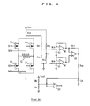
- Fig. 4 illustrates an example of such a circuit.
- the reference numeral 12 denotes a coil that is disposed between the mid-point between a first FET 14 and a second FET 16, and the mid-point between a third FET 15 and a fourth FET 17.
- the reference numerals S1 to S4 are gate signals to the FETs 14 to 17.
- the reference numerals R8 to R18 denote resistors.
- R10 is a sensing resistor and R8, R9 are resistors for generating a reference potential of a comparator 22.
- the reference numeral Vcc denotes a power supply, for instance of 12 V or 30 V, of the coil 12, and Vcc2 denotes a power supply, for instance, of 5 V.
- the reference numerals 40, 41 denote buffers, and the reference numeral 42 denotes a differential amplifier.
- the voltage of the sensing resistor R10 is monitored, since the first and second FETs 14, 15 break down on account of overcurrent when a ground fault occurs.
- the sensing precision of the circuit of Fig. 4 drops due to variability in the resistors R11 to R14.
- a differential amplifier circuit comprising the buffers 40, 41 and the differential amplifier 42, is thus required. This entails a non-negligible cost in order to drive several tens of coils 12 connected in parallel. Therefore, the inventors studied detection of ground faults in inductive loads using small-scale circuits, and arrived as a result at the present invention.
- the drive circuit for an inductive load of the present invention is provided with: an inductive load disposed between a midpoint between a first and a second transistor connected in series and a midpoint between a third and a fourth transistor connected in series;
- switching of the inductive load is controlled through switching on/off of the first to fourth transistors
- the detection means comprises a comparator that compares the voltage applied to the sensing resistor with the threshold value, and means for detecting that a comparator signal does not change for the predetermined time or longer, and for turning off the drive signals.
- duty ratios at which the first and third transistors are switched on are each greater than duty ratios at which the second and fourth transistors are switched on, in such a manner that the fourth transistor is switched on/off during the period over which the first transistor is switched on, and the second transistor is switched on/off during the period over which the third transistor is switched on.
- the on-duty ratio of the first transistor need not be identical to the on-duty ratio of the third transistor.
- the on-duty ratio of the second transistor need not be identical to the on-duty ratio of the fourth transistor.
- ground shorts can be detected accurately, also at the inductive load, by detecting ground shorts when the voltage applied to the sensing resistor is continuously equal to or lower, for a predetermined period of time or longer, than a threshold value for ground short detection. Detection of ground shorts, however, is delayed in the above procedure.
- a protective resistor is provided to lower the potential at the source or emitter of the first or third transistor, to limit as a result the current at the first or third transistor, and prolong thereby the time until breakdown due to overcurrent from a ground short.
- the detection means can be configured in a simple manner using a comparator that compares a voltage applied to the sensing resistor with a threshold value, and means for detecting that a comparator signal does not change for a predetermined time or longer, and for turning off the drive signals.
- the duty ratios at which the first and third transistors are switched on are each greater than the duty ratios at which the second and fourth transistors are switched on, in such a manner that the fourth transistor is switched on/off during the period over which the first transistor is switched on, and the second transistor is switched on/off during the period over which the third transistor is switched on.
- the first and third transistors on the high-potential side may have a lower speed than the second and fourth transistors on the low-potential side. This allows reducing component costs.
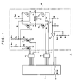
- Figs. 1 to 3 illustrate a drive circuit for an inductive load 2.
- the reference numeral 4 denotes a gate array, which may also be a microprocessor or the like
- the reference numeral 6 denotes an individual circuit provided for each coil 12
- the reference numerals 8, 9 denote each a drive IC for driving the individual circuit 6, such that for instance several tens of individual circuits 6 are driven in parallel.
- the individual circuit 6 outputs a ground fault detection signal from the comparator 22.
- the detected signal is inputted into a flip-flop array 10 provided in the gate array 4, such that the drive circuit 2 is stopped when a ground fault is detected.
- the reference numeral 12 denotes a coil, herein a solenoid coil, but which may also be a simple coil, a brushless motor coil or the like.
- the reference numerals 14 to 17 denote switching FETs, from among which FETs 14, 15 are high-voltage FETs according to the power supply Vcc, and the FETs 16, 17 are low-voltage FETs. The switching time of FETs 16, 17 is shorter than that of FETs 14, 15.
- FETs 14, 16 are disposed in series, between a protective resistor R1 on the side of the power supply Vcc and a sensing resistor R2 on the ground side.
- FETs 15, 17 are disposed in series between the protective resistor R1 and the sensing resistor R2.
- the coil 12 is disposed between the midpoint between FETs 14, 16 and the midpoint between FETs 15, 17.
- the reference numeral S denotes the sources, D the drains and G the gates of FETs 14, 15.
- R4 to R7 denote resistors for determining the potential of a gate signal G that is applied to FETs 14, 15.
- the reference numeral R3 is a resistor on the input side of the comparator 22, C1 is a capacitor, and R8, R9 are resistors for generating a reference potential of the comparator 22.
- the power supply Vcc is set, for instance to 30 V or 12 V, and the power supply Vcc2 to 5 V or 3 V. However, the power supply Vcc2 may be omitted, in which case only the power supply Vcc is provided.
- the protective resistor R1 and the sensing resistor R2 have a resistance, for instance, ranging from about 0.1 to 10 ⁇ .
- the drive circuit 2 is built into an actuator of a knitted fabric pl-down apparatus in a flat knitting machine.
- the drive circuit 2 drives a pawl or locking member for pulling a knitted fabric down, by way of a solenoid having the coil 12 built thereinto.
- the coil 12 is energized not only upon switching of the solenoid state, but also after switching of the solenoid state, as well as upon switching to a rise position (Set) and a sink position (Reset) of the solenoid.
- Several tens of individual circuits 6 are disposed in parallel in the pull-down apparatus. The individual circuits 6 are controlled by the gate array 4 and the drive ICs 8, 9.
- the drive circuit 2 may also be used in a solenoid for controlling carrier hauling, or a solenoid for driving cams in the carriage of a flat knitting machine.
- the drive circuit 2 can be used, for instance, for driving brushless motor coils.
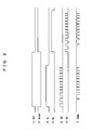
- Fig. 2 illustrates drive waveforms at the individual circuit 6.
- Fig. 2 , 1 depicts the waveform of a set signal for setting the rise position of a solenoid through energization of the coil 12 from the FET 14 side to the FET 17 side; 2) depicts the waveform of a reset signal for resetting the solenoid through energization from FET 15 to the FET 16 side.
- the set signal and the reset signal are virtual signals in the drive ICs 8, 9.
- Fig. 2 , 3 depicts the waveform of a signal Su that is applied to the gate of FET 14, and 4) depicts the waveform of a signal Ru that is applied to the gate of FET 15.
- the widths of the signals Su, Ru are shorter than the widths of the signal Set and the signal Reset, but may be identical to the widths of the latter.
- Fig. 2 , 5) depicts the waveform of a signal Sd that is applied to the gate of FET 17, and 6) depicts the waveform of a signal Rd that is applied to the gate of FET 16.
- the signals in 3) to 6) are depicted as active HIGH, but in actuality are active LOW signals.
- Fig. 3 1
- Fig. 3 1
- the duty ratio at which the gate signal is switched on is initially high but smaller later on.
- the response of the coil 12 to the switching of FETs 14 to 17 is slow.
- the current flows as illustrated in 2), such that the same current flows through the sensing resistor R2 in the absence of a ground fault.
- the threshold value of the comparator 22 is determined as indicated by the dashed line of 2) in Fig. 3 , whereupon the output of the comparator changes as depicted in 3) of Fig. 3 . If both FETs 16, 17 are off, the output of the comparator is kept HIGH.
- the current flowing through the sensing resistor R2 is small during a short time after switching of the state of the coil 12, even when FET 16 or 17 is on.
- T1 is set as a time longer than the time elapsed since switching of the state of the coil 12 until the current flowing through the sensing resistor R2 is equal to or greater than the threshold value. This time is also set to be longer than one period upon switching control of FETs 16, 17. An anomaly is deemed to have occurred in the individual circuit 6 if the comparator 22 does not output even a single LOW during the time T1, i.e. if the state of the comparator 22 does not change during the time T1.
- the protective resistor R1 is provided in order to make the time until breakdown ofFETs 14, 15 longer than the ground fault detection period T1.
- the source potential of FETs 14, 15 drops on account of protective resistor R1, and the gate potential difference decreases.
- the current flowing through FETs 14, 15 is limited thereby, and the time until breakdown can be made longer than the above period T1.
- the current flowing through the sensing resistor R2 becomes substantially 0.
- the voltage of the sensing resistor R2 varies in synchrony with the switching on/off of FETs 16, 17, but this variation is small.
- the above variation is detected by the comparator 22.
- the detection threshold value is determined by the resistors R8, R9, but the threshold value may also be generated by way of a Zener diode or the like, instead of resistors.
- the flip-flop array 10 of the gate array 4 detects that the comparator 22 has not changed to LOW even a single time during the period T1. For instance, a flip-flop circuit is provided in the flip-flop array 10 for each individual circuit 6, such that each flip-flop circuit is set at the LOW signal from the comparator 22.
- the presence or absence of ground faults can be detected by checking the output of the flip-flop circuit every period T1, and by resetting next the flip-flop circuit. Upon detection of a ground fault, for instance, the flat knitting machine is stopped, an anomaly is displayed, and driving of all the individual circuits 6 is discontinued, to prevent breakdown of FETs 14 to 17.
- the present embodiment describes an application in the pull-down apparatus of a flat knitting machine, but the drive circuit 2 may be used for any other application.
- the switches used in the embodiment are FET switches 14 to 17, but bipolar transistors or the like may also be used for switching.
- the bases ofPNP bipolar transistors are disposed at the positions of the gates, emitters at the position of the sources, and collectors at the position of the drains, ofFETs 14, 15 in the embodiment.
- FETs 14, 15 are driven with wide pulses, and FETs 16, 17 with narrow pulses, in order to reduce the influence of, for instance, parasitic capacitance at the high-voltage FETs 14, 15.
- narrow pulses may be applied for instance to FETs 14, 15, and wide pulses to FETs 16, 17, in a case where FETs 14, 15 are high-speed FETs.
- the coil 12 is controlled through switching, but the embodiment is not limited thereto.
Landscapes
- Engineering & Computer Science (AREA)
- Power Engineering (AREA)
- Electronic Switches (AREA)
Abstract
Description
- The present invention relates to a drive circuit for inductive loads such as solenoids, motors and coils, and more particularly to detection of ground faults around inductive loads.
- Patent document 1:
JP 11-81105 A JP 11-81105 A - Patent document 2:
JP 62-6663 Y2 - Ground faults (shorts to ground) must be detected upon driving of inductive loads such as solenoids or the like. Patent document 3:
JP 2005-210871 A Fig. 4 illustrates an example of such a circuit. In the figure, thereference numeral 12 denotes a coil that is disposed between the mid-point between afirst FET 14 and asecond FET 16, and the mid-point between athird FET 15 and afourth FET 17. The reference numerals S1 to S4 are gate signals to theFETs 14 to 17. The reference numerals R8 to R18 denote resistors. Among these, R10 is a sensing resistor and R8, R9 are resistors for generating a reference potential of acomparator 22. The reference numeral Vcc denotes a power supply, for instance of 12 V or 30 V, of thecoil 12, and Vcc2 denotes a power supply, for instance, of 5 V. Thereference numerals reference numeral 42 denotes a differential amplifier. The voltage of the sensing resistor R10 is monitored, since the first andsecond FETs - The sensing precision of the circuit of
Fig. 4 drops due to variability in the resistors R11 to R14. A differential amplifier circuit, comprising thebuffers differential amplifier 42, is thus required. This entails a non-negligible cost in order to drive several tens ofcoils 12 connected in parallel. Therefore, the inventors studied detection of ground faults in inductive loads using small-scale circuits, and arrived as a result at the present invention. - Patent document 1:
JP 11-81105 A - Patent document 2:
JP 62-6663 Y2 - Patent document 3:
JP 2005-210871 A - It is an object of the present invention to allow detecting ground shorts using a simple, low-cost circuit, and to prevent breakdown of drive transistors.
- The drive circuit for an inductive load of the present invention is provided with: an inductive load disposed between a midpoint between a first and a second transistor connected in series and a midpoint between a third and a fourth transistor connected in series;
- a protective resistor disposed between sources or emitters of the first and third transistors and a direct-current power supply, and a sensing resistor disposed between low-potential sides of the second and fourth transistors and ground;
- drive means for driving the first and third transistors through input of drive signals, each having a fixed potential, to gates or bases thereof; and
- detection means for switching off the drive signals from the drive means when, during powering of the inductive load, a voltage applied to the sensing resistor is continuously equal to or lower, for a predetermined period of time or longer, than a threshold value for ground short detection.
- Preferably, switching of the inductive load is controlled through switching on/off of the first to fourth transistors, and
the detection means comprises a comparator that compares the voltage applied to the sensing resistor with the threshold value, and means for detecting that a comparator signal does not change for the predetermined time or longer, and for turning off the drive signals.
More preferably, duty ratios at which the first and third transistors are switched on are each greater than duty ratios at which the second and fourth transistors are switched on, in such a manner that the fourth transistor is switched on/off during the period over which the first transistor is switched on, and the second transistor is switched on/off during the period over which the third transistor is switched on. The on-duty ratio of the first transistor need not be identical to the on-duty ratio of the third transistor. The on-duty ratio of the second transistor need not be identical to the on-duty ratio of the fourth transistor. - The current flowing to a sensing resistor decreases when a ground short occurs. However, the current response to a control signal is delayed at the inductive load, and hence the current flowing to a sensing resistor may be small in some cases, even in a normal state. Therefore, ground shorts can be detected accurately, also at the inductive load, by detecting ground shorts when the voltage applied to the sensing resistor is continuously equal to or lower, for a predetermined period of time or longer, than a threshold value for ground short detection. Detection of ground shorts, however, is delayed in the above procedure. Therefore, a protective resistor is provided to lower the potential at the source or emitter of the first or third transistor, to limit as a result the current at the first or third transistor, and prolong thereby the time until breakdown due to overcurrent from a ground short. The above configuration allows detecting ground shorts accurately, and preventing breakdown of the first or third transistor, while avoiding loss of sensing precision at the resistor bridge and greater costs incurred by a differential amplifier circuit.
- The detection means can be configured in a simple manner using a comparator that compares a voltage applied to the sensing resistor with a threshold value, and means for detecting that a comparator signal does not change for a predetermined time or longer, and for turning off the drive signals.
Further, the duty ratios at which the first and third transistors are switched on are each greater than the duty ratios at which the second and fourth transistors are switched on, in such a manner that the fourth transistor is switched on/off during the period over which the first transistor is switched on, and the second transistor is switched on/off during the period over which the third transistor is switched on. Thereby, the first and third transistors on the high-potential side may have a lower speed than the second and fourth transistors on the low-potential side. This allows reducing component costs. -
-
Fig. 1 is a block diagram of a drive circuit in an example; -
Fig. 2 is a set of waveform diagrams in an example, wherein 1) depicts the waveform of a set signal Set, 2) depicts the waveform of a reset signal Reset, 3) depicts the waveform of a gate signal Su of a setting FET on a high-potential side, 4) depicts the waveform of a gate signal Ru of a resetting FET on a high-potential side, 5) depicts the waveform of a gate signal Sd of a setting FET on a low-potential side, 6) depicts the waveform of a gate signal Rd of a resetting FET on a low-potential side, and 7) depicts a signal of a comparator for ground fault detection; -
Fig. 3 is a set of waveform diagrams of current flowing through a sensing resistor in an example, wherein 1) depicts a gate signal in a low-potential side FET, 2) depicts current flowing through a sensing resistor, and 3) depicts a comparator signal; and -
Fig. 4 is a block diagram of a drive circuit in a conventional example. -
- 2
- drive circuit
- 4
- gate array
- 6
- individual circuit
- 8, 9
- drive IC
- 10
- flip-flop array
- 12
- coil
- 14 to 17
- FET
- 20,21
- FET
- 22
- comparator
- 40, 41
- buffer
- 42
- differential amplifier
- R1 to R18
- resistor
- C1 to C4
- capacitor
- Vcc, Vcc2
- power supply
- Preferred embodiments of the present invention are described below.
-
Figs. 1 to 3 illustrate a drive circuit for aninductive load 2. InFig. 1 , thereference numeral 4 denotes a gate array, which may also be a microprocessor or the like, thereference numeral 6 denotes an individual circuit provided for eachcoil 12, the reference numerals 8, 9 denote each a drive IC for driving theindividual circuit 6, such that for instance several tens ofindividual circuits 6 are driven in parallel. Theindividual circuit 6 outputs a ground fault detection signal from thecomparator 22. The detected signal is inputted into a flip-flop array 10 provided in thegate array 4, such that thedrive circuit 2 is stopped when a ground fault is detected. - In the
individual circuit 6, thereference numeral 12 denotes a coil, herein a solenoid coil, but which may also be a simple coil, a brushless motor coil or the like. The reference numerals 14 to 17 denote switching FETs, from among whichFETs FETs FETs FETs FETs FETs coil 12 is disposed between the midpoint betweenFETs FETs FETs -
FET 20drives FET 14, andFET 21drives FET 15.FETs FETs comparator 22, C1 is a capacitor, and R8, R9 are resistors for generating a reference potential of thecomparator 22. The power supply Vcc is set, for instance to 30 V or 12 V, and the power supply Vcc2 to 5 V or 3 V. However, the power supply Vcc2 may be omitted, in which case only the power supply Vcc is provided. The protective resistor R1 and the sensing resistor R2 have a resistance, for instance, ranging from about 0.1 to 10 Ω. - The
drive circuit 2 is built into an actuator of a knitted fabric pl-down apparatus in a flat knitting machine. For instance, thedrive circuit 2 drives a pawl or locking member for pulling a knitted fabric down, by way of a solenoid having thecoil 12 built thereinto. Thecoil 12 is energized not only upon switching of the solenoid state, but also after switching of the solenoid state, as well as upon switching to a rise position (Set) and a sink position (Reset) of the solenoid. Several tens ofindividual circuits 6 are disposed in parallel in the pull-down apparatus. Theindividual circuits 6 are controlled by thegate array 4 and the drive ICs 8, 9. Other than in the knitted fabric pull-down apparatus of a flat knitting machine, thedrive circuit 2 may also be used in a solenoid for controlling carrier hauling, or a solenoid for driving cams in the carriage of a flat knitting machine. In addition, thedrive circuit 2 can be used, for instance, for driving brushless motor coils. -
Fig. 2 illustrates drive waveforms at theindividual circuit 6. InFig. 2 ,1 ) depicts the waveform of a set signal for setting the rise position of a solenoid through energization of thecoil 12 from theFET 14 side to theFET 17 side; 2) depicts the waveform of a reset signal for resetting the solenoid through energization fromFET 15 to theFET 16 side. The set signal and the reset signal are virtual signals in the drive ICs 8, 9. InFig. 2 ,3 ) depicts the waveform of a signal Su that is applied to the gate ofFET 14, and 4) depicts the waveform of a signal Ru that is applied to the gate ofFET 15. In the present embodiment, the widths of the signals Su, Ru are shorter than the widths of the signal Set and the signal Reset, but may be identical to the widths of the latter. InFig. 2 , 5) depicts the waveform of a signal Sd that is applied to the gate ofFET 17, and 6) depicts the waveform of a signal Rd that is applied to the gate ofFET 16. The signals in 3) to 6) are depicted as active HIGH, but in actuality are active LOW signals. - When the signals Su, Sd are both HIGH, a setting current flows through the
coil 12. When the signals Ru, Rd are both HIGH, there flows a reset signal. Thecoil 12 is chopped and the rise is slow until the current stabilizes on account of the inductive load. Therefore, a higher duty ratio is set initially for the signals Sd, Rd. The duty ratio is reduced subsequently. At the LOW period of signals Su, Ru, the duty ratio is for instance set to 0. The corresponding output waveform of thecomparator 22 is depicted in 7) ofFig. 2 . This waveform is a waveform when there is no ground fault. - In
Fig. 3 ,1 ) depicts the current flowing through the gate signal ofFETs comparator 22. The duty ratio at which the gate signal is switched on is initially high but smaller later on. The response of thecoil 12 to the switching ofFETs 14 to 17 is slow. InFig. 3 , therefore, the current flows as illustrated in 2), such that the same current flows through the sensing resistor R2 in the absence of a ground fault. The threshold value of thecomparator 22 is determined as indicated by the dashed line of 2) inFig. 3 , whereupon the output of the comparator changes as depicted in 3) ofFig. 3 . If bothFETs coil 12, even whenFET - Accordingly, T1 is set as a time longer than the time elapsed since switching of the state of the
coil 12 until the current flowing through the sensing resistor R2 is equal to or greater than the threshold value. This time is also set to be longer than one period upon switching control ofFETs individual circuit 6 if thecomparator 22 does not output even a single LOW during the time T1, i.e. if the state of thecomparator 22 does not change during the time T1. - The operation in the present embodiment is explained returning to
Fig. 1 . To set the solenoid,FET 14 andFET 17 are switched on with the waveform ofFig. 2 .FET 15 andFET 16 are operated to reset the solenoid. An overcurrent flows throughFET 14 orFET 15 when a ground fault occurs on account of a wiring short during assembly of the solenoid, or when a ground fault occurs for some other cause after assembly. The points of ground fault occurrence are indicated by P1, P2 inFig. 1 . For instance, overcurrent flows throughFET 14, and the latter breaks down, when a ground fault occurs at point P1. Likewise, overcurrent flows throughFET 15, and the latter breaks down, when a ground fault occurs at point P2. The protective resistor R1 is provided in order to make the time untilbreakdown ofFETs FETs FETs - When a ground fault occurs, the current flowing through the sensing resistor R2 becomes substantially 0. Normally, the voltage of the sensing resistor R2 varies in synchrony with the switching on/off of
FETs comparator 22. The detection threshold value is determined by the resistors R8, R9, but the threshold value may also be generated by way of a Zener diode or the like, instead of resistors. Next, the flip-flop array 10 of thegate array 4 detects that thecomparator 22 has not changed to LOW even a single time during the period T1. For instance, a flip-flop circuit is provided in the flip-flop array 10 for eachindividual circuit 6, such that each flip-flop circuit is set at the LOW signal from thecomparator 22. The presence or absence of ground faults can be detected by checking the output of the flip-flop circuit every period T1, and by resetting next the flip-flop circuit. Upon detection of a ground fault, for instance, the flat knitting machine is stopped, an anomaly is displayed, and driving of all theindividual circuits 6 is discontinued, to prevent breakdown ofFETs 14 to 17. - The following effects are elicited in the present embodiment.
- (1) No resistor bridge of
Fig. 4 is used for ground fault detection. Accordingly, no errors occur on account of resistor variability. - (2) No differential amplifying circuit is required for ground fault detection.
- (3) Accordingly, ground faults can be detected with high precision using a small-scale circuit, whereby ground fault detection costs can be reduced.
- (4) Ground faults are detected on the basis of the absence of even a single change to LOW by the
comparator 22 during a time T1 that is shorter than the breakdown time ofFETs coil 12 is switched and controlled by theFETs 14 to 17. - (5) The time required for ground fault detection is at most T1. Therefore, the breakdown time of
FETs - The present embodiment describes an application in the pull-down apparatus of a flat knitting machine, but the
drive circuit 2 may be used for any other application. Also, the switches used in the embodiment areFET switches 14 to 17, but bipolar transistors or the like may also be used for switching. In this case, the bases ofPNP bipolar transistors are disposed at the positions of the gates, emitters at the position of the sources, and collectors at the position of the drains,ofFETs FETs FETs voltage FETs FETs FETs coil 12 is controlled through switching, but the embodiment is not limited thereto.
Claims (3)
- A drive circuit for an inductive load, characterized by comprising:an inductive load disposed between a midpoint between a first and a second transistor connected in series and a midpoint between a third and a fourth transistor connected in series;a protective resistor disposed between sources or emitters of the first and third transistors and a direct-current power supply, and a sensing resistor disposed between low-potential sides of the second and fourth transistors and ground;drive means for driving the first and third transistors through input of drive signals, each having a fixed potential, to gates or bases thereof; anddetection means for switching off the drive signals from the drive means when, during powering of the inductive load, a voltage applied to the sensing resistor is continuously equal to or lower, for a predetermined period of time or longer, than a threshold value for ground short detection.
- The drive circuit for an inductive load according to claim 1, characterized in that
switching of the inductive load is controlled through switching on/off of the first to fourth transistors,
and in that
the detection means comprises a comparator that compares the voltage applied to the sensing resistor with the threshold value, and means for detecting that a comparator signal does not change for the predetermined time or longer, and for turning off the drive signals. - The drive circuit for an inductive load according to claim 1 or 2, characterized in that duty ratios at which the first and third transistors are switched on are each greater than duty ratios at which the second and fourth transistors are switched on, in such a manner that the fourth transistor is switched on/off during the period over which the first transistor is switched on, and the second transistor is switched on/off during the period over which the third transistor is switched on.
Applications Claiming Priority (2)
| Application Number | Priority Date | Filing Date | Title |
|---|---|---|---|
| JP2008037273 | 2008-02-19 | ||
| PCT/JP2009/052491 WO2009104535A1 (en) | 2008-02-19 | 2009-02-16 | Drive circuit for inductive load |
Publications (3)
| Publication Number | Publication Date |
|---|---|
| EP2246968A1 true EP2246968A1 (en) | 2010-11-03 |
| EP2246968A4 EP2246968A4 (en) | 2015-01-07 |
| EP2246968B1 EP2246968B1 (en) | 2017-05-17 |
Family
ID=40985416
Family Applications (1)
| Application Number | Title | Priority Date | Filing Date |
|---|---|---|---|
| EP09712300.4A Not-in-force EP2246968B1 (en) | 2008-02-19 | 2009-02-16 | Drive circuit for inductive load |
Country Status (4)
| Country | Link |
|---|---|
| EP (1) | EP2246968B1 (en) |
| JP (1) | JP5436230B2 (en) |
| CN (1) | CN102067422B (en) |
| WO (1) | WO2009104535A1 (en) |
Cited By (1)
| Publication number | Priority date | Publication date | Assignee | Title |
|---|---|---|---|---|
| EP2717445A1 (en) * | 2012-10-04 | 2014-04-09 | Schneider Toshiba Inverter Europe SAS | Control method in a power converter to ensure the detectability of a short-circuit |
Families Citing this family (5)
| Publication number | Priority date | Publication date | Assignee | Title |
|---|---|---|---|---|
| JP6122257B2 (en) * | 2012-07-04 | 2017-04-26 | ローム株式会社 | DC / DC converter and control circuit thereof, power supply using the same, power adapter, and electronic device |
| CN102780383B (en) * | 2012-07-18 | 2014-10-08 | 华为技术有限公司 | Silicon controlled rectifier driving method and device |
| FR3013919B1 (en) * | 2013-11-22 | 2016-01-08 | Continental Automotive France | SHORT-CIRCUIT DETECTION IN A SWITCHING STRUCTURE |
| CN106464247B (en) * | 2014-05-28 | 2019-07-23 | 夏普株式会社 | Drive circuit |
| TWI587612B (en) * | 2015-03-10 | 2017-06-11 | 立錡科技股份有限公司 | Power converter, switch control circuit and short circuit detection method for current sensing resistor of the power converter |
Family Cites Families (5)
| Publication number | Priority date | Publication date | Assignee | Title |
|---|---|---|---|---|
| JPS6025113U (en) | 1983-07-27 | 1985-02-20 | 横河電機株式会社 | solenoid drive circuit |
| JP3457161B2 (en) | 1997-09-05 | 2003-10-14 | 株式会社島精機製作所 | Fabric lowering device for flat knitting machine |
| JP2005210871A (en) | 2004-01-26 | 2005-08-04 | Toshiba Corp | Motor drive control device and motor current detection method |
| JP2007074794A (en) * | 2005-09-06 | 2007-03-22 | Rohm Co Ltd | Overcurrent protective circuit, load driving unit, motor driving unit, electrical equipment, and power unit |
| JP4823650B2 (en) * | 2005-11-16 | 2011-11-24 | ローム株式会社 | Inverter and driving method thereof, and light emitting device and liquid crystal television using the same |
-
2009
- 2009-02-16 WO PCT/JP2009/052491 patent/WO2009104535A1/en not_active Ceased
- 2009-02-16 JP JP2009554294A patent/JP5436230B2/en not_active Expired - Fee Related
- 2009-02-16 CN CN200980105683.4A patent/CN102067422B/en not_active Expired - Fee Related
- 2009-02-16 EP EP09712300.4A patent/EP2246968B1/en not_active Not-in-force
Non-Patent Citations (2)
| Title |
|---|
| LAI R S ET AL: "A PWM METHOD FOR REDUCTION OF SWITCHING LOSS IN A FULL-BRIDGE INVERTER", PROCEEDINGS OF THE ANNUAL APPLIED POWER ELECTRONICS CONFERENCE AND EXPOSITION (APEC). ORLANDO, FEB. 13 - 17, 1994; [PROCEEDINGS OF THE ANNUAL APPLIED POWER ELECTRONICS CONFERENCE AND EXPOSITION (APEC)], NEW YORK, IEEE, US, vol. 1, 13 February 1994 (1994-02-13), pages 122-127, XP000467309, * |
| See also references of WO2009104535A1 * |
Cited By (2)
| Publication number | Priority date | Publication date | Assignee | Title |
|---|---|---|---|---|
| EP2717445A1 (en) * | 2012-10-04 | 2014-04-09 | Schneider Toshiba Inverter Europe SAS | Control method in a power converter to ensure the detectability of a short-circuit |
| FR2996697A1 (en) * | 2012-10-04 | 2014-04-11 | Schneider Toshiba Inverter | CONTROL METHOD IMPLEMENTED IN A POWER CONVERTER TO ENSURE THE DETECTABILITY OF A SHORT-CIRCUIT |
Also Published As
| Publication number | Publication date |
|---|---|
| CN102067422A (en) | 2011-05-18 |
| EP2246968A4 (en) | 2015-01-07 |
| EP2246968B1 (en) | 2017-05-17 |
| JP5436230B2 (en) | 2014-03-05 |
| JPWO2009104535A1 (en) | 2011-06-23 |
| WO2009104535A1 (en) | 2009-08-27 |
| CN102067422B (en) | 2014-03-26 |
Similar Documents
| Publication | Publication Date | Title |
|---|---|---|
| CN205725692U (en) | For driving the gate driver circuit of power switch | |
| EP2246968B1 (en) | Drive circuit for inductive load | |
| US8373957B2 (en) | Load driving circuit and protection method | |
| US10992244B2 (en) | Load driving circuit | |
| KR101350545B1 (en) | Level shifter circuit and gate driver circuit including the same | |
| JP6365330B2 (en) | Abnormality detection circuit | |
| US20120013323A1 (en) | Half bridge apparatus and half bridge control method | |
| US20030020420A1 (en) | Actuator drive circuit | |
| JP2017028649A (en) | Semiconductor integrated circuit | |
| JP2017212583A (en) | Protection circuit of semiconductor element | |
| JP3577478B2 (en) | Inverter device | |
| EP1800394A2 (en) | Current limiting circuit for high-speed low-side driver outputs | |
| KR101529149B1 (en) | Three phase aprratus for driving gate | |
| JP5810973B2 (en) | Switching element drive circuit | |
| JP2016192695A (en) | Inductive load drive unit | |
| JP5423624B2 (en) | Overcurrent protection circuit | |
| JP4727360B2 (en) | Gate circuit of insulated gate semiconductor device | |
| JP2014216703A (en) | Load drive circuit | |
| JP4214948B2 (en) | Load drive circuit | |
| JP2007525875A (en) | High voltage pulse driver using capacitive coupling | |
| CN107112961B (en) | gate drive circuit | |
| JP2007146336A (en) | Knitting machine | |
| JP4124363B2 (en) | PWM output circuit | |
| KR100856760B1 (en) | DC power supply control circuit with multiple control inputs | |
| JP5452399B2 (en) | Semiconductor device |
Legal Events
| Date | Code | Title | Description |
|---|---|---|---|
| PUAI | Public reference made under article 153(3) epc to a published international application that has entered the european phase |
Free format text: ORIGINAL CODE: 0009012 |
|
| 17P | Request for examination filed |
Effective date: 20100817 |
|
| AK | Designated contracting states |
Kind code of ref document: A1 Designated state(s): AT BE BG CH CY CZ DE DK EE ES FI FR GB GR HR HU IE IS IT LI LT LU LV MC MK MT NL NO PL PT RO SE SI SK TR |
|
| AX | Request for extension of the european patent |
Extension state: AL BA RS |
|
| DAX | Request for extension of the european patent (deleted) | ||
| REG | Reference to a national code |
Ref country code: DE Ref legal event code: R079 Ref document number: 602009046122 Country of ref document: DE Free format text: PREVIOUS MAIN CLASS: H02M0007480000 Ipc: H02M0001320000 |
|
| A4 | Supplementary search report drawn up and despatched |
Effective date: 20141210 |
|
| RIC1 | Information provided on ipc code assigned before grant |
Ipc: H02M 7/5387 20070101ALI20141204BHEP Ipc: H02M 1/32 20070101AFI20141204BHEP Ipc: H02M 7/48 20070101ALI20141204BHEP |
|
| 17Q | First examination report despatched |
Effective date: 20151207 |
|
| GRAP | Despatch of communication of intention to grant a patent |
Free format text: ORIGINAL CODE: EPIDOSNIGR1 |
|
| INTG | Intention to grant announced |
Effective date: 20161207 |
|
| GRAS | Grant fee paid |
Free format text: ORIGINAL CODE: EPIDOSNIGR3 |
|
| GRAA | (expected) grant |
Free format text: ORIGINAL CODE: 0009210 |
|
| AK | Designated contracting states |
Kind code of ref document: B1 Designated state(s): AT BE BG CH CY CZ DE DK EE ES FI FR GB GR HR HU IE IS IT LI LT LU LV MC MK MT NL NO PL PT RO SE SI SK TR |
|
| REG | Reference to a national code |
Ref country code: GB Ref legal event code: FG4D |
|
| REG | Reference to a national code |
Ref country code: CH Ref legal event code: EP |
|
| REG | Reference to a national code |
Ref country code: IE Ref legal event code: FG4D |
|
| REG | Reference to a national code |
Ref country code: AT Ref legal event code: REF Ref document number: 895276 Country of ref document: AT Kind code of ref document: T Effective date: 20170615 |
|
| REG | Reference to a national code |
Ref country code: DE Ref legal event code: R096 Ref document number: 602009046122 Country of ref document: DE |
|
| REG | Reference to a national code |
Ref country code: NL Ref legal event code: MP Effective date: 20170517 |
|
| REG | Reference to a national code |
Ref country code: LT Ref legal event code: MG4D |
|
| REG | Reference to a national code |
Ref country code: AT Ref legal event code: MK05 Ref document number: 895276 Country of ref document: AT Kind code of ref document: T Effective date: 20170517 |
|
| PG25 | Lapsed in a contracting state [announced via postgrant information from national office to epo] |
Ref country code: HR Free format text: LAPSE BECAUSE OF FAILURE TO SUBMIT A TRANSLATION OF THE DESCRIPTION OR TO PAY THE FEE WITHIN THE PRESCRIBED TIME-LIMIT Effective date: 20170517 Ref country code: NO Free format text: LAPSE BECAUSE OF FAILURE TO SUBMIT A TRANSLATION OF THE DESCRIPTION OR TO PAY THE FEE WITHIN THE PRESCRIBED TIME-LIMIT Effective date: 20170817 Ref country code: AT Free format text: LAPSE BECAUSE OF FAILURE TO SUBMIT A TRANSLATION OF THE DESCRIPTION OR TO PAY THE FEE WITHIN THE PRESCRIBED TIME-LIMIT Effective date: 20170517 Ref country code: GR Free format text: LAPSE BECAUSE OF FAILURE TO SUBMIT A TRANSLATION OF THE DESCRIPTION OR TO PAY THE FEE WITHIN THE PRESCRIBED TIME-LIMIT Effective date: 20170818 Ref country code: LT Free format text: LAPSE BECAUSE OF FAILURE TO SUBMIT A TRANSLATION OF THE DESCRIPTION OR TO PAY THE FEE WITHIN THE PRESCRIBED TIME-LIMIT Effective date: 20170517 Ref country code: FI Free format text: LAPSE BECAUSE OF FAILURE TO SUBMIT A TRANSLATION OF THE DESCRIPTION OR TO PAY THE FEE WITHIN THE PRESCRIBED TIME-LIMIT Effective date: 20170517 Ref country code: ES Free format text: LAPSE BECAUSE OF FAILURE TO SUBMIT A TRANSLATION OF THE DESCRIPTION OR TO PAY THE FEE WITHIN THE PRESCRIBED TIME-LIMIT Effective date: 20170517 |
|
| PG25 | Lapsed in a contracting state [announced via postgrant information from national office to epo] |
Ref country code: LV Free format text: LAPSE BECAUSE OF FAILURE TO SUBMIT A TRANSLATION OF THE DESCRIPTION OR TO PAY THE FEE WITHIN THE PRESCRIBED TIME-LIMIT Effective date: 20170517 Ref country code: NL Free format text: LAPSE BECAUSE OF FAILURE TO SUBMIT A TRANSLATION OF THE DESCRIPTION OR TO PAY THE FEE WITHIN THE PRESCRIBED TIME-LIMIT Effective date: 20170517 Ref country code: PL Free format text: LAPSE BECAUSE OF FAILURE TO SUBMIT A TRANSLATION OF THE DESCRIPTION OR TO PAY THE FEE WITHIN THE PRESCRIBED TIME-LIMIT Effective date: 20170517 Ref country code: IS Free format text: LAPSE BECAUSE OF FAILURE TO SUBMIT A TRANSLATION OF THE DESCRIPTION OR TO PAY THE FEE WITHIN THE PRESCRIBED TIME-LIMIT Effective date: 20170917 Ref country code: SE Free format text: LAPSE BECAUSE OF FAILURE TO SUBMIT A TRANSLATION OF THE DESCRIPTION OR TO PAY THE FEE WITHIN THE PRESCRIBED TIME-LIMIT Effective date: 20170517 Ref country code: BG Free format text: LAPSE BECAUSE OF FAILURE TO SUBMIT A TRANSLATION OF THE DESCRIPTION OR TO PAY THE FEE WITHIN THE PRESCRIBED TIME-LIMIT Effective date: 20170817 |
|
| PG25 | Lapsed in a contracting state [announced via postgrant information from national office to epo] |
Ref country code: EE Free format text: LAPSE BECAUSE OF FAILURE TO SUBMIT A TRANSLATION OF THE DESCRIPTION OR TO PAY THE FEE WITHIN THE PRESCRIBED TIME-LIMIT Effective date: 20170517 Ref country code: DK Free format text: LAPSE BECAUSE OF FAILURE TO SUBMIT A TRANSLATION OF THE DESCRIPTION OR TO PAY THE FEE WITHIN THE PRESCRIBED TIME-LIMIT Effective date: 20170517 Ref country code: SK Free format text: LAPSE BECAUSE OF FAILURE TO SUBMIT A TRANSLATION OF THE DESCRIPTION OR TO PAY THE FEE WITHIN THE PRESCRIBED TIME-LIMIT Effective date: 20170517 Ref country code: RO Free format text: LAPSE BECAUSE OF FAILURE TO SUBMIT A TRANSLATION OF THE DESCRIPTION OR TO PAY THE FEE WITHIN THE PRESCRIBED TIME-LIMIT Effective date: 20170517 Ref country code: CZ Free format text: LAPSE BECAUSE OF FAILURE TO SUBMIT A TRANSLATION OF THE DESCRIPTION OR TO PAY THE FEE WITHIN THE PRESCRIBED TIME-LIMIT Effective date: 20170517 |
|
| REG | Reference to a national code |
Ref country code: DE Ref legal event code: R097 Ref document number: 602009046122 Country of ref document: DE |
|
| PLBE | No opposition filed within time limit |
Free format text: ORIGINAL CODE: 0009261 |
|
| STAA | Information on the status of an ep patent application or granted ep patent |
Free format text: STATUS: NO OPPOSITION FILED WITHIN TIME LIMIT |
|
| 26N | No opposition filed |
Effective date: 20180220 |
|
| PG25 | Lapsed in a contracting state [announced via postgrant information from national office to epo] |
Ref country code: SI Free format text: LAPSE BECAUSE OF FAILURE TO SUBMIT A TRANSLATION OF THE DESCRIPTION OR TO PAY THE FEE WITHIN THE PRESCRIBED TIME-LIMIT Effective date: 20170517 |
|
| REG | Reference to a national code |
Ref country code: CH Ref legal event code: PL |
|
| PG25 | Lapsed in a contracting state [announced via postgrant information from national office to epo] |
Ref country code: MC Free format text: LAPSE BECAUSE OF FAILURE TO SUBMIT A TRANSLATION OF THE DESCRIPTION OR TO PAY THE FEE WITHIN THE PRESCRIBED TIME-LIMIT Effective date: 20170517 |
|
| GBPC | Gb: european patent ceased through non-payment of renewal fee |
Effective date: 20180216 |
|
| REG | Reference to a national code |
Ref country code: IE Ref legal event code: MM4A |
|
| REG | Reference to a national code |
Ref country code: BE Ref legal event code: MM Effective date: 20180228 |
|
| PG25 | Lapsed in a contracting state [announced via postgrant information from national office to epo] |
Ref country code: LU Free format text: LAPSE BECAUSE OF NON-PAYMENT OF DUE FEES Effective date: 20180216 Ref country code: LI Free format text: LAPSE BECAUSE OF NON-PAYMENT OF DUE FEES Effective date: 20180228 Ref country code: CH Free format text: LAPSE BECAUSE OF NON-PAYMENT OF DUE FEES Effective date: 20180228 |
|
| REG | Reference to a national code |
Ref country code: FR Ref legal event code: ST Effective date: 20181031 |
|
| PG25 | Lapsed in a contracting state [announced via postgrant information from national office to epo] |
Ref country code: IE Free format text: LAPSE BECAUSE OF NON-PAYMENT OF DUE FEES Effective date: 20180216 |
|
| PG25 | Lapsed in a contracting state [announced via postgrant information from national office to epo] |
Ref country code: GB Free format text: LAPSE BECAUSE OF NON-PAYMENT OF DUE FEES Effective date: 20180216 Ref country code: BE Free format text: LAPSE BECAUSE OF NON-PAYMENT OF DUE FEES Effective date: 20180228 Ref country code: FR Free format text: LAPSE BECAUSE OF NON-PAYMENT OF DUE FEES Effective date: 20180228 |
|
| PG25 | Lapsed in a contracting state [announced via postgrant information from national office to epo] |
Ref country code: MT Free format text: LAPSE BECAUSE OF NON-PAYMENT OF DUE FEES Effective date: 20180216 |
|
| PG25 | Lapsed in a contracting state [announced via postgrant information from national office to epo] |
Ref country code: TR Free format text: LAPSE BECAUSE OF FAILURE TO SUBMIT A TRANSLATION OF THE DESCRIPTION OR TO PAY THE FEE WITHIN THE PRESCRIBED TIME-LIMIT Effective date: 20170517 |
|
| PG25 | Lapsed in a contracting state [announced via postgrant information from national office to epo] |
Ref country code: PT Free format text: LAPSE BECAUSE OF FAILURE TO SUBMIT A TRANSLATION OF THE DESCRIPTION OR TO PAY THE FEE WITHIN THE PRESCRIBED TIME-LIMIT Effective date: 20170517 Ref country code: HU Free format text: LAPSE BECAUSE OF FAILURE TO SUBMIT A TRANSLATION OF THE DESCRIPTION OR TO PAY THE FEE WITHIN THE PRESCRIBED TIME-LIMIT; INVALID AB INITIO Effective date: 20090216 |
|
| PG25 | Lapsed in a contracting state [announced via postgrant information from national office to epo] |
Ref country code: CY Free format text: LAPSE BECAUSE OF FAILURE TO SUBMIT A TRANSLATION OF THE DESCRIPTION OR TO PAY THE FEE WITHIN THE PRESCRIBED TIME-LIMIT Effective date: 20170517 Ref country code: MK Free format text: LAPSE BECAUSE OF NON-PAYMENT OF DUE FEES Effective date: 20170517 |
|
| PGFP | Annual fee paid to national office [announced via postgrant information from national office to epo] |
Ref country code: DE Payment date: 20231220 Year of fee payment: 16 |
|
| PGFP | Annual fee paid to national office [announced via postgrant information from national office to epo] |
Ref country code: IT Payment date: 20240111 Year of fee payment: 16 |
|
| REG | Reference to a national code |
Ref country code: DE Ref legal event code: R119 Ref document number: 602009046122 Country of ref document: DE |
|
| PG25 | Lapsed in a contracting state [announced via postgrant information from national office to epo] |
Ref country code: DE Free format text: LAPSE BECAUSE OF NON-PAYMENT OF DUE FEES Effective date: 20250902 |
|
| PG25 | Lapsed in a contracting state [announced via postgrant information from national office to epo] |
Ref country code: IT Free format text: LAPSE BECAUSE OF NON-PAYMENT OF DUE FEES Effective date: 20250216 |