EP2317501B1 - Verfahren und Vorrichtung zur Ansteuerung einer Flüssigkristallanzeige - Google Patents
Verfahren und Vorrichtung zur Ansteuerung einer Flüssigkristallanzeige Download PDFInfo
- Publication number
- EP2317501B1 EP2317501B1 EP10163162.0A EP10163162A EP2317501B1 EP 2317501 B1 EP2317501 B1 EP 2317501B1 EP 10163162 A EP10163162 A EP 10163162A EP 2317501 B1 EP2317501 B1 EP 2317501B1
- Authority
- EP
- European Patent Office
- Prior art keywords
- control signal
- pixel
- polarity control
- gate
- image data
- Prior art date
- Legal status (The legal status is an assumption and is not a legal conclusion. Google has not performed a legal analysis and makes no representation as to the accuracy of the status listed.)
- Active
Links
Images


Classifications
-
- G—PHYSICS
- G09—EDUCATION; CRYPTOGRAPHY; DISPLAY; ADVERTISING; SEALS
- G09G—ARRANGEMENTS OR CIRCUITS FOR CONTROL OF INDICATING DEVICES USING STATIC MEANS TO PRESENT VARIABLE INFORMATION
- G09G3/00—Control arrangements or circuits, of interest only in connection with visual indicators other than cathode-ray tubes
- G09G3/20—Control arrangements or circuits, of interest only in connection with visual indicators other than cathode-ray tubes for presentation of an assembly of a number of characters, e.g. a page, by composing the assembly by combination of individual elements arranged in a matrix no fixed position being assigned to or needed to be assigned to the individual characters or partial characters
- G09G3/34—Control arrangements or circuits, of interest only in connection with visual indicators other than cathode-ray tubes for presentation of an assembly of a number of characters, e.g. a page, by composing the assembly by combination of individual elements arranged in a matrix no fixed position being assigned to or needed to be assigned to the individual characters or partial characters by control of light from an independent source
- G09G3/36—Control arrangements or circuits, of interest only in connection with visual indicators other than cathode-ray tubes for presentation of an assembly of a number of characters, e.g. a page, by composing the assembly by combination of individual elements arranged in a matrix no fixed position being assigned to or needed to be assigned to the individual characters or partial characters by control of light from an independent source using liquid crystals
- G09G3/3611—Control of matrices with row and column drivers
- G09G3/3614—Control of polarity reversal in general
-
- G—PHYSICS
- G09—EDUCATION; CRYPTOGRAPHY; DISPLAY; ADVERTISING; SEALS
- G09G—ARRANGEMENTS OR CIRCUITS FOR CONTROL OF INDICATING DEVICES USING STATIC MEANS TO PRESENT VARIABLE INFORMATION
- G09G3/00—Control arrangements or circuits, of interest only in connection with visual indicators other than cathode-ray tubes
- G09G3/20—Control arrangements or circuits, of interest only in connection with visual indicators other than cathode-ray tubes for presentation of an assembly of a number of characters, e.g. a page, by composing the assembly by combination of individual elements arranged in a matrix no fixed position being assigned to or needed to be assigned to the individual characters or partial characters
- G09G3/34—Control arrangements or circuits, of interest only in connection with visual indicators other than cathode-ray tubes for presentation of an assembly of a number of characters, e.g. a page, by composing the assembly by combination of individual elements arranged in a matrix no fixed position being assigned to or needed to be assigned to the individual characters or partial characters by control of light from an independent source
- G09G3/36—Control arrangements or circuits, of interest only in connection with visual indicators other than cathode-ray tubes for presentation of an assembly of a number of characters, e.g. a page, by composing the assembly by combination of individual elements arranged in a matrix no fixed position being assigned to or needed to be assigned to the individual characters or partial characters by control of light from an independent source using liquid crystals
- G09G3/3607—Control arrangements or circuits, of interest only in connection with visual indicators other than cathode-ray tubes for presentation of an assembly of a number of characters, e.g. a page, by composing the assembly by combination of individual elements arranged in a matrix no fixed position being assigned to or needed to be assigned to the individual characters or partial characters by control of light from an independent source using liquid crystals for displaying colours or for displaying grey scales with a specific pixel layout, e.g. using sub-pixels
-
- G—PHYSICS
- G09—EDUCATION; CRYPTOGRAPHY; DISPLAY; ADVERTISING; SEALS
- G09G—ARRANGEMENTS OR CIRCUITS FOR CONTROL OF INDICATING DEVICES USING STATIC MEANS TO PRESENT VARIABLE INFORMATION
- G09G2310/00—Command of the display device
- G09G2310/02—Addressing, scanning or driving the display screen or processing steps related thereto
- G09G2310/0202—Addressing of scan or signal lines
- G09G2310/0213—Addressing of scan or signal lines controlling the sequence of the scanning lines with respect to the patterns to be displayed, e.g. to save power
-
- G—PHYSICS
- G09—EDUCATION; CRYPTOGRAPHY; DISPLAY; ADVERTISING; SEALS
- G09G—ARRANGEMENTS OR CIRCUITS FOR CONTROL OF INDICATING DEVICES USING STATIC MEANS TO PRESENT VARIABLE INFORMATION
- G09G2310/00—Command of the display device
- G09G2310/02—Addressing, scanning or driving the display screen or processing steps related thereto
- G09G2310/0264—Details of driving circuits
- G09G2310/0297—Special arrangements with multiplexing or demultiplexing of display data in the drivers for data electrodes, in a pre-processing circuitry delivering display data to said drivers or in the matrix panel, e.g. multiplexing plural data signals to one D/A converter or demultiplexing the D/A converter output to multiple columns
-
- G—PHYSICS
- G09—EDUCATION; CRYPTOGRAPHY; DISPLAY; ADVERTISING; SEALS
- G09G—ARRANGEMENTS OR CIRCUITS FOR CONTROL OF INDICATING DEVICES USING STATIC MEANS TO PRESENT VARIABLE INFORMATION
- G09G2320/00—Control of display operating conditions
- G09G2320/02—Improving the quality of display appearance
- G09G2320/0247—Flicker reduction other than flicker reduction circuits used for single beam cathode-ray tubes
-
- G—PHYSICS
- G09—EDUCATION; CRYPTOGRAPHY; DISPLAY; ADVERTISING; SEALS
- G09G—ARRANGEMENTS OR CIRCUITS FOR CONTROL OF INDICATING DEVICES USING STATIC MEANS TO PRESENT VARIABLE INFORMATION
- G09G2320/00—Control of display operating conditions
- G09G2320/06—Adjustment of display parameters
- G09G2320/0686—Adjustment of display parameters with two or more screen areas displaying information with different brightness or colours
-
- G—PHYSICS
- G09—EDUCATION; CRYPTOGRAPHY; DISPLAY; ADVERTISING; SEALS
- G09G—ARRANGEMENTS OR CIRCUITS FOR CONTROL OF INDICATING DEVICES USING STATIC MEANS TO PRESENT VARIABLE INFORMATION
- G09G2330/00—Aspects of power supply; Aspects of display protection and defect management
- G09G2330/02—Details of power systems and of start or stop of display operation
- G09G2330/021—Power management, e.g. power saving
-
- G—PHYSICS
- G09—EDUCATION; CRYPTOGRAPHY; DISPLAY; ADVERTISING; SEALS
- G09G—ARRANGEMENTS OR CIRCUITS FOR CONTROL OF INDICATING DEVICES USING STATIC MEANS TO PRESENT VARIABLE INFORMATION
- G09G2360/00—Aspects of the architecture of display systems
- G09G2360/16—Calculation or use of calculated indices related to luminance levels in display data
Definitions
- the present invention relates generally to a liquid crystal display (LCD), and more particularly, to a source driver of a display panel for displaying an image data in an adaptive column inversion and methods of driving same.
- LCD liquid crystal display
- LCD Liquid crystal display
- An LCD apparatus includes an LCD panel formed with liquid crystal cells and pixel elements with each associating with a corresponding liquid crystal cell and having a liquid crystal capacitor and a storage capacitor, a thin film transistor (TFT) electrically coupled with the liquid crystal capacitor and the storage capacitor.
- TFT thin film transistor
- These pixel elements are substantially arranged in the form of a matrix having a number of pixel rows and a number of pixel columns.
- scanning signals generated from a gate driver, are sequentially applied to the number of pixel rows, through a plurality of scanning lines along the row direction, for sequentially turning on the pixel elements row-by-row.
- source signals of an image to be displayed, generated from a source driver, for the pixel row are simultaneously applied to the number of pixel columns, through a plurality of data lines arranged crossing over the plurality of scanning lines along the column direction, so as to charge the corresponding liquid crystal capacitor and storage capacitor of the pixel row for aligning orientations of the corresponding liquid crystal cells associated with the pixel row to control light transmittance therethrough.
- all pixel elements are supplied with corresponding source signals of the image signal, thereby displaying the image signal thereon.
- Liquid crystal molecules have a definite orientational alignment as a result of their long, thin shapes.
- the orientations of liquid crystal molecules in liquid crystal cells of an LCD panel play a crucial role in the transmittance of light therethrough. It is known if a substantially high voltage is applied between the liquid crystal layer for a long period of time, the optical transmission characteristics of the liquid crystal molecules may change. This change may be permanent, causing an irreversible degradation in the display quality of the LCD panel.
- the polarity of the voltage signals applied on the LC cell has to be changed continuously.
- a source driver is configured to generate such voltage signals having their polarity alternated according to an inversion scheme such as frame inversion, row inversion, column inversion, dot inversion, or 2-line inversion.
- the display quality of an image in a dot inversion or a 2-line inversion is better than that in other inversion schemes; however, the power consumption is higher comparing to that in the other inversion schemes.
- the column invention may result in a low consumption of power, but there are issues such as crosstalks and vertical flickers.
- the display quality of an image is similar to that of the dot inversion, while its power consumption is similar to that of the column invention.
- crosstalks and horizontal bright and dark lines may occur in the zig-zag scheme.
- US 2006/0092120 A1 and US 2006/0022929 A1 both describe a liquid crystal display device having a control unit, a gate driving unit, a data driving unit and a liquid crystal panel.
- EP 2 075 788 A2 and US 2003/227428 A1 describe alternative signal-line driving circuits for a liquid crystal display.
- US 2006/0092120 A1 in particular includes a LCD controlling unit which is configured to control a liquid crystal panel.
- the controlling unit includes an image judging unit and a method determining unit.
- the image judging unit is configured to compare a gradation of each pixel of image data with a reference gradation.
- the method determining unit is configured to determine an inversion driving method for displaying the image data on the liquid crystal panel every plurality of pixels of less than one frame in the image data as a selection inversion driving method based on the comparison result.
- the present invention relates to a source driver for driving a display panel to display an image data in an adaptive column inversion, where the display panel comprises a plurality of pixels spatially arranged in a matrix form and a plurality of data lines, each data line being associated with pixels of a corresponding pixel column, where the image data is decomposed into a number of frames, and each frame of the image data is mapped onto the pixel matrix with grey levels such that a grey level associated with a pixel is corresponding to the shade of grey of the frame to be displayed at the pixel.
- the source driver includes a data processing unit adapted for determining the grey levels of the image data mapped onto the pixel matrix, a MUX coupled to the data processing unit and adapted for receiving a frame polarity control signal, FramePOL, and a pixel polarity control signal, XPOL, and outputting a polarity control signal, POL, that is corresponding one of FramePOL and XPOL according to the determined grey levels of the image data, and a switch module coupled to the MUX and controlled by the polarity control signal POL, a first digital-to-analog converter with a positive polarity (PDAC) adapted for receiving a first digital signal associated with the image data and converting the first digital signal into a first analog signal, a second digital-to-analog converter with a negative polarity (NDAC) adapted for receiving a second digital signal associated with the image data and converting the second digital signal into a second analog signal, a first operational amplifier coupled to the PDAC and the NDAC through
- the data processing unit comprises a logic circuit adapted for determining N most-significant bits (MSBs) of the image data mapped onto two neighboring data lines, such that when all of the N MSBs is equal to 1 or 0, the output of the logic circuit is 1, otherwise, the output of the logic circuit is 0, N being a positive integer, where when the output of the logic circuit is 1, the MUX selects the frame polarity control signal FramePOL, and when the output of the logic circuit is 0, the MUX selects the pixel polarity control signal POL.
- N 4.
- the first and second analog signals have positive and negative polarities, respectively.
- the first and second data signals have positive and negative polarities, respectively.
- the polarity control signal POL has a low state and a high state, where when the polarity control signal POL is in the high state, each odd data line of the plurality of data line receives the first data signal, while each even data line of the plurality of data line receives the second data signal, and where when the polarity control signal POL is in the low state, each odd data line of the plurality of data line receives the second data signal, while each even data line of the plurality of data line receives the first data signal.
- the present invention relates to a source driver for driving a display panel to display an image data in an adaptive column inversion, where the display panel comprises a plurality of pixels spatially arranged in a matrix form and a plurality of data lines, each data line being associated with pixels of a corresponding pixel column, where the image data is decomposed into a number of frames, and each frame of the image data is mapped onto the pixel matrix with grey levels such that a grey level associated with a pixel is corresponding to the shade of grey of the frame to be displayed at the pixel.
- the source driver includes a data processing unit having a logic circuit adapted for determining N MSBs of image data signals mapped onto two neighboring data lines, such that when all of the N MSBs is equal to 1 or 0, the output of the logic circuit is 1, otherwise, the output of the logic circuit is 0, where N is a positive integer, and a MUX coupled to the data processing unit and adapted for receiving a frame polarity control signal, FramePOL, and a pixel polarity control signal, XPOL, and selectively outputting the frame polarity control signal FramePOL when the output of the logic circuit is 1, or the pixel polarity control signal POL when the output of the logic circuit is 0, as a polarity control signal, POL.
- pixels of the pixel matrix associated with the neighboring data lines are driven with a column inversion, while the other pixels of the pixel matrix are driven with one of a dot inversion and a 2-line inversion.
- the source driver further includes a switch module coupled to the MUX and controlled by the polarity control signal POL, a PDAC adapted for receiving a first digital signal associated with the image data and converting the first digital signal into a first analog signal, a NDAC adapted for receiving a second digital signal associated with the image data and converting the second digital signal into a second analog signal, a first operational amplifier coupled to the PDAC and the NDAC through the switch module and adapted for receiving one of the first analog signal from the PDAC and the second analog signal from the NDAC and outputting a first data signal to an odd data line of the plurality of data line, and a second operational amplifier coupled to the PDAC and the NDAC through the switch module and adapted for receiving the other of the first analog signal from the PDAC and the second analog signal from the NDAC and outputting a second data signal to an even data line of the plurality of data line.
- a switch module coupled to the MUX and controlled by the polarity control signal POL
- PDAC adapted for receiving a first digital
- the first and second analog signals have positive and negative polarities, respectively.
- the first and second data signals have positive and negative polarities, respectively.
- the polarity control signal POL has a low state and a high state, where when the polarity control signal POL is in the high state, each odd data line of the plurality of data line receives the first data signal, while each even data line of the plurality of data line receives the second data signal, and where when the polarity control signal POL is in the low state, each odd data line of the plurality of data line receives the second data signal, while each even data line of the plurality of data line receives the first data signal.
- the present invention relates to a method for driving a display panel to display an image data in an adaptive column inversion, where the display panel comprises a plurality of pixels spatially arranged in a matrix form and a plurality of data lines, each data line being associated with pixels of a corresponding pixel column.
- the method comprises the steps of inputting an image data to be displayed, where the image data is decomposed into a number of frames, and each frame of the image data is mapped onto the pixel matrix with grey levels such that a grey level associated with a pixel is corresponding to the shade of grey of the frame to be displayed at the pixel, determining N MSBs of image data signals mapped onto two neighboring data lines, N being a positive integer, selecting a frame polarity control signal, FramePOL, when all of the N MSBs of the image data signals mapped onto the two neighboring data lines is equal to 1 or 0, or a pixel polarity control signal, XPOL, when the N MSBs comprise 1 and 0, as a polarity control signal, POL, and displaying the image data in a column inversion in pixels of the pixel matrix when the frame polarity control signal FramePOL is selected and in one of a dot inversion and a 2-line inversion in the other pixels of the pixel matrix when the pixel polarity control
- the determining step is performed with a data processing unit having a logic circuit adapted such that when all of the N MSBs is equal to 1 or 0, the output of the logic circuit is 1, otherwise, the output of the logic circuit is 0, where N is a positive integer.
- the selecting step is performed with a MUX adapted such that when the output of the logic circuit is 1, the MUX selects the frame polarity control signal FramePOL, and when the output of the logic circuit is 0, the MUX selects the pixel polarity control signal POL.
- the present invention relates to a source driver for driving a display panel to display an image data in an adaptive column inversion, wherein the display panel comprises a plurality of pixels spatially arranged in a matrix form and a plurality of data lines, each data line being associated with pixels of a corresponding pixel column, wherein the image data is decomposed into a number of frames, and wherein each frame of the image data is mapped onto the pixel matrix with grey levels such that a grey level associated with a pixel is corresponding to the shade of grey of the frame to be displayed at the pixel.
- the source driver comprises a MUX coupled to the data processing unit and adapted for receiving a frame polarity control signal, FramePOL, and a pixel polarity control signal, XPOL, and selectively outputting the frame polarity control signal FramePOL when the output of the logic circuit is 1, or the pixel polarity control signal POL when the output of the logic circuit is 0, as a polarity control signal, POL, and a plurality of driver modules coupled to the MUX, each driver module adapted for receiving two corresponding image data signals and selectively outputting them to a corresponding odd data line and a corresponding even data line of the 2n neighboring data lines according to the control signal POL.
- the logic circuit comprises a plurality of EX-NOR gates and an AND gate coupled to the plurality of EX-NOR gates, adapted for determining N most-significant bits (MSBs) of the image data signals mapped onto each 2n neighboring data lines, such that when all of the N MSBs are equal to 1 or 0, the output of the logic circuit is 1, otherwise, the output of the logic circuit is 0, wherein N is a positive integer.
- MSBs most-significant bits
- the driver module has a switch module coupled to the MUX and controlled by the polarity control signal POL, a first digital-to-analog converter with a positive polarity (PDAC) adapted for receiving a first digital signal associated with the image data and converting the first digital signal into a first analog signal, a second digital-to-analog converter with a negative polarity (NDAC) adapted for receiving a second digital signal associated with the image data and converting the second digital signal into a second analog signal, a first operational amplifier coupled to the PDAC and the NDAC through the switch module and adapted for receiving one of the first analog signal from the PDAC and the second analog signal from the NDAC and outputting a first data signal to an odd data line of the plurality of data line, and a second operational amplifier coupled to the PDAC and the NDAC through the switch module and adapted for receiving the other of the first analog signal from the PDAC and the second analog signal from the NDAC and outputting a second data signal to an even data line of the plurality of
- pixels of the pixel matrix associated with the 2n neighboring data lines are driven with a column inversion, while the other pixels of the pixel matrix are driven with one of a dot inversion and a 2-line inversion.
- control signal POL is the frame polarity control signal FramePOL, and otherwise the polarity control signal POL is the pixel polarity control signal XPOL.
- grey level refers to one of (discrete) shades of grey for an image, or an amount of light perceived by a human for the image. If the brightness of the image is expressed in the form of shades of grey in n bits, n being an integer greater than zero, the grey level takes values from zero representing black, up to (2 n - 1) representing white, with intermediate values representing increasingly light shades of grey. In an LCD device, the amount of light that transmits through liquid crystals is adjusted to represent the grey level.
- this invention in one aspect, relates to a source driver for driving a display panel to display an image data in an adaptive column inversion.
- the display panel has a plurality of pixels spatially arranged in a matrix form and a plurality of data lines, each data line being associated with pixels of a corresponding pixel column.
- the image data is decomposed into a number of frames, where each frame of the image data is mapped onto the pixel matrix with grey levels such that a grey level associated with a pixel is corresponding to the shade of grey of the frame to be displayed at the pixel.
- the image data is processed by for example, a video device (not shown), into a plurality of image data signals expressed in the form of grey levels in k bits, and each image data signal is input to a corresponding data line for display in a pixel column associated with the corresponding data line.
- a video device not shown
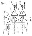
- the source driver 100 includes, among other components, a data processing unit 110, a MUX 120 coupled to the data processing unit 110, a switch module 130 coupled to the MUX 120, a first digital-to-analog converter with a positive polarity (PDAC) 141, a second digital-to-analog converter with a negative polarity (NDAC) 142, and a first operational amplifier 151 and a second operational amplifier 152 coupled to the PDAC 141 and the NDAC 142 through the switch module 130.
- PDAC positive polarity
- NDAC negative polarity
- the data processing unit 110 is adapted for determining the grey levels of the image data 190 mapped onto the pixel matrix, so as to select one or more inversion driving methods to drive the display panel to display the image.
- the data processing unit 110 determines the grey levels of image data signals 190 associated with (or input to) two neighboring data lines 171 and 172.
- the data processing unit 110 determines N most-significant bits (MSBs) of the image data signals 190.
- the MUX 120 is adapted for receiving a frame polarity control signal, FramePOL, and a pixel polarity control signal, XPOL, and outputting a polarity control signal, POL, that is corresponding one of FramePOL and XPOL according to the determined grey levels of the image data.
- the polarity control signal POL is the frame polarity control signal FramePOL
- Ln and Lm are two predetermined grey levels.
- pixels of the pixel matrix associated with the determined grey levels are driven with a column inversion, and the other pixels of the pixel matrix are driven with one of a dot inversion and a 2-line inversion.
- the pixel polarity control signal XPOL is generated from a timing controller (T-con, not shown) and used to determine a data inversion scheme.
- the switch module 130 may includes a pair of switches SW1 and SW2 that are coupled to the PDAC 141, the NDAC 142, the first operational amplifier 151 and the second operational amplifier 152 and controlled by the polarity control signal POL. For example, when the polarity control signal POL is in a high state (H), the output signals of the PDAC 141, the NDAC 142 are respectively delivered to the first operational amplifier 151 and the second operational amplifier 152. Otherwise, when the polarity control signal POL is in a low state (L), the output signals of the PDAC 141, the NDAC 142 are respectively delivered to the second operational amplifier 152 and the first operational amplifier 151.
- H high state
- L low state
- the PDAC 141 is adapted for receiving a first digital signal 191 of the image data and converting the first digital signal 191 into a first analog signal.
- the NDAC 142 is adapted for receiving a second digital signal 192 of the image data and converting the second digital signal 192 into a second analog signal.
- the image data 190 and the first digital signal 191 and the second digital signal 192 are processed of the image to be displayed.
- the image data 190 includes at least the first digital signal 191 and the second digital signal 192.
- the first and second analog signals have positive and negative polarities, respectively.
- the first operational amplifier 151 and the second operational amplifier 152 are coupled to the PDAC 141 and the NDAC 142 through the switch module 130.
- the first operational amplifier 151 is adapted for receiving one of the first analog signal from the PDAC 141 and the second analog signal from the NDAC 142, and outputting a first data signal to an odd data line 161
- the second operational amplifier 152 is adapted for receiving the other of the first analog signal from the PDAC 141 and the second analog signal from the NDAC 142 and outputting a second data signal to an even data line 162.
- the first and second data signals have positive and negative polarities, respectively.
- the odd data line 161 receives the first data signal, while the even data line 162 receives the second data signal, and when the polarity control signal POL is in the low state (L), the odd data line 161 receives the second data signal, while the even data line 162 receives the first data signal.
- the data processing unit 110 includes a logic circuit for determining N MSBs of the image data mapped onto two neighboring data lines.
- the logic circuit includes a first EX-NOR gate 111, a second EX-NOR gate 112 and an AND gate 113 coupled to each other.
- N 4.
- the output of the first EX-NOR gate 111 (or the second EX-NOR gate 112) is true, indicated by 1, only when all of four inputs are the same, i.e., all of the four inputs are 0 or all of the four inputs are 1 in the binary. Otherwise, it is false.
- the output of the AND gate 113 is true, indicated by 1, only when all of the outputs of the first EX-NOR gate 111 and the second EX-NOR gate 112 are true (1).
- the first EX-NOR gate 111 and the second EX-NOR gate 112 are utilized to determine four (4) MSBs of data signals of two neighboring data lines, respectively.
- the output of the logic circuit is true, indicated by 1. Otherwise, the output of the logic circuit is false, indicated by 0.
- the MUX selects the frame polarity control signal FramePOL as the polarity control signal POL, i.e., a column inversion.
- the MUX selects the pixel polarity control signal XPOL as the polarity control signal POL, i.e., a dot inversion or a 2-dot inversion.
- Fig. 3(a) shows schematically an image displayed with a 2-dot inversion.
- Fig. 3(b) shows schematically the image displayed with an adaptive column inversion, that is, S1 and S2 columns are in the column inversion, and S3 and S4 column are in the 2-dot inversion.
- YDIO is corresponding to a start pulse of image frames.
- Each frame has a polarity, FramePOL, which is opposite to that of its immediately prior and/or next frame.
- FramePOL changes every frame.
- XSTB rising edge latch XPOL determines the polarity of each horizontal line.
- Figs. 5 and 6 are two consecutive frames of an image displayed with an adaptive column inversion.
- FramePOL is adapted to control the PDAC, the NDAC, the first and second operational amplifiers, accordingly, the image is displayed in a column inversion.
- FramePOL is adapted to control the PDAC, the NDAC, the first and second operational amplifiers, accordingly, the image is displayed in a column inversion.
- XPOL is adapted to control the PDAC, the NDAC, the first and second operational amplifiers, accordingly, the image is displayed in a 2-dot column inversion, as indicated in area 510.
- the present invention relates to a method for driving a display panel to display an image data in an adaptive column inversion.
- the method includes the following steps: at first, an image data to be displayed is provided.
- the image data is decomposed into a number of frames, where each frame of the image data is mapped onto the pixel matrix with grey levels such that a grey level associated with a pixel is corresponding to the shade of grey of the frame to be displayed at the pixel.
- N MSBs of image data signals mapped onto two neighboring data lines are determined.
- a frame polarity control signal FramePOL is selected as a polarity control signal POL, or when the N MSBs comprise 1 and 0, a pixel polarity control signal XPOL is selected as the polarity control signal, POL.
- the image data is displayed in a column inversion in pixels of the pixel matrix when the frame polarity control signal FramePOL is selected and in one of a dot inversion and a 2-line inversion in the other pixels of the pixel matrix when the pixel polarity control signal XPOL is selected.
- the determining step is performed with a data processing unit having a logic circuit adapted such that when all of the N MSBs is equal to 1 or 0, the output of the logic circuit is 1, otherwise, the output of the logic circuit is 0, wherein N is a positive integer.
- the selecting step is performed with a MUX adapted such that when the output of the logic circuit is 1, the MUX selects the frame polarity control signal FramePOL, and when the output of the logic circuit is 0, the MUX selects the pixel polarity control signal POL.
- Fig. 7 shows schematically a block diagram of a source driver 700 according to another embodiment of the present invention.
- the source driver 700 comprises a data processing unit 710, a MUX 720 coupled to the data processing unit 710, and a plurality of driver modules, DM1, DM2, ..., DMn, 780 coupled to the MUX 720.
- the logic circuit includes 2n EX-NOR gates, D1, D2, ..., D2n, and an AND gate coupled to the 2n EX-NOR gates, D1, D2, ..., D2n.
- Each EX-NOR gate is configured to receive a corresponding image data signal and output 0 or 1 based on the input image data signal. Specifically, if all of N most-significant bits (MSBs) of the input image data signal are equal to 1, or 0, the EX-NOR gate outputs 1, otherwise, it outputs 0. When all of N most-significant bits (MSBs) of the input image data signal are equal to 1, the grey levels of the input image data signal are greater than Lm. When all of N most-significant bits (MSBs) of the input image data signal are equal to 0, the grey levels of the input image data signal are less than Ln.
- the MUX 720 is coupled to the logic circuit and adapted for receiving a frame polarity control signal, FramePOL, and a pixel polarity control signal, XPOL.
- the MUX 720 selects the frame polarity control signal FramePOL as the polarity control signal POL, i.e., a column inversion.
- the MUX 720 selects the pixel polarity control signal XPOL as the polarity control signal POL, i.e., a dot inversion or a 2-dot inversion.
- Each driver module 780 is adapted for receiving two corresponding image data signals 791 and 792 and selectively outputting them to a corresponding odd data line 761 and a corresponding even data line 762 of the 2n neighboring data lines, S1, S2, ..., S2n, according to the control signal POL.
- the corresponding odd data line 761 is one of S1, S3, ..., S2n-1, while the corresponding even data line 762 if one of S2, S4, ..., S2n.
- the driver module 780 has a switch module 730 coupled to the MUX 720, a first digital-to-analog converter with a positive polarity (PDAC) 741, a second digital-to-analog converter with a negative polarity (NDAC) 742, and a first operational amplifier 751 and a second operational amplifier 752 coupled to the PDAC 741 and the NDAC 742 through the switch module 730.
- PDAC positive polarity
- NDAC negative polarity
- the switch module 730 may includes a pair of switches SW1 and SW2 that are coupled to the PDAC 741, the NDAC 742, the first operational amplifier 751 and the second operational amplifier 752 and controlled by the polarity control signal POL. For example, when the polarity control signal POL is in a high state (H), the output signals of the PDAC 741, the NDAC 742 are respectively delivered to the first operational amplifier 751 and the second operational amplifier 752. Otherwise, when the polarity control signal POL is in a low state (L), the output signals of the PDAC 741, the NDAC 742 are respectively delivered to the second operational amplifier 752 and the first operational amplifier 751.
- H high state
- L low state
- the PDAC 741 is adapted for receiving a first digital signal 791 of the image data and converting the first digital signal 791 into a first analog signal.
- the NDAC 742 is adapted for receiving a second digital signal 792 of the image data and converting the second digital signal 792 into a second analog signal.
- the image data 790 and the first digital signal 791 and the second digital signal 792 are processed of the image to be displayed.
- the image data 790 includes at least the first digital signal 791 and the second digital signal 792.
- the first and second analog signals have positive and negative polarities, respectively.
- the first operational amplifier 751 and the second operational amplifier 752 are coupled to the PDAC 741 and the NDAC 742 through the switch module 730.
- the first operational amplifier 751 is adapted for receiving one of the first analog signal from the PDAC 741 and the second analog signal from the NDAC 742, and outputting a first data signal to an odd data line 761
- the second operational amplifier 752 is adapted for receiving the other of the first analog signal from the PDAC 741 and the second analog signal from the NDAC 742 and outputting a second data signal to an even data line 762.
- the first and second data signals have positive and negative polarities, respectively.
- pixels of the pixel matrix associated with the 2n neighboring data lines S1, S2, ..., S2n are driven with a column inversion, while the other pixels of the pixel matrix are driven with one of a dot inversion and a 2-line inversion.
- the display quality of an image in a display device can be substantially improved, while the power consumption can be reduced significantly.
Landscapes
- Engineering & Computer Science (AREA)
- Chemical & Material Sciences (AREA)
- Crystallography & Structural Chemistry (AREA)
- Physics & Mathematics (AREA)
- Computer Hardware Design (AREA)
- General Physics & Mathematics (AREA)
- Theoretical Computer Science (AREA)
- Control Of Indicators Other Than Cathode Ray Tubes (AREA)
- Liquid Crystal (AREA)
- Liquid Crystal Display Device Control (AREA)
Claims (2)
- Quelltreiber (100) zur Ansteuerung eines Anzeigepanels zur Anzeige von Bilddaten (190) mit einer adaptiven Spalteninversion, wobei das Anzeigepanel eine Vielzahl von Pixeln, die räumlich in einer Matrixform angeordnet sind, und eine Vielzahl von Datenleitungen umfasst, wobei jede Datenleitung den Pixeln einer korrespondierenden Pixelspalte zugeordnet ist, wobei die Bilddaten (190) in eine Mehrzahl von Datenübertragungsblöcken (Frames) zerlegt werden, und wobei jeder Datenübertragungsblock der Bilddaten (190) mit Grauwerten auf die Pixelmatrix abgebildet wird, sodass ein mit einem Pixel assoziierter Grauwert der Grauschattierung des Datenübertragungsblocks, der an dem Pixel angezeigt werden soll, entspricht, umfassend:(a) eine Datenverarbeitungseinheit (110, 710), die ausgebildet ist, die Grauwerte der auf die Pixelmatrix abgebildeten Bilddatensignale zu bestimmen, wobei die Datenverarbeitungseinheit (110, 710) eine Logikschaltung umfasst, und wobei die Logikschaltung ein erstes Gatter (111), ein zweites Gatter (112) und ein UND-Gatter (AND gate) (113) umfasst, das mit dem ersten Gatter (111) und dem zweiten Gatter (112) gekoppelt ist, wobei die Logikschaltung zur Bestimmung der N höchstsignifikantesten Bits (MSBs) der auf zwei benachbarte Datenleitungen abgebildeten Bilddaten und zur jeweiligen Bereitstellung der N MSBs an das erste Gatter und das zweite Gatter ausgebildet ist, wobei, wenn alle der N MSBs, die in das erste Gatter (111) eingespeist werden, gleich 1 sind oder wenn alle der in das erste Gatter (111) eingespeisten N MSBs gleich 0 sind, die Ausgabe des ersten Gatters (111) 1 ist, wobei ansonsten die Ausgabe des ersten Gatters (111) 0 ist, wobei, wenn alle der N MSBs, die in das zweite Gatter (112) eingespeist werden, gleich 1 sind oder wenn alle der in das zweite Gatter (112) eingespeisten N MSBs gleich 0 sind, die Ausgabe des zweiten Gatters (112) 1 ist, wobei ansonsten die Ausgabe des zweiten Gatters (112) 0 ist, wobei die Ausgabe des UND-Gatters (113) 1 ist, wenn die Ausgaben des ersten Gatters (111) und des zweiten Gatters (112) 1 sind, wobei ansonsten die Ausgabe des UND-Gatters (113) 0 ist,(b) einen Multiplexer (MUX) (120, 720), der mit der Datenverarbeitungseinheit (110,710) gekoppelt ist und konfiguriert ist, ein Polaritätskontollsignal für den Datenübertragungsblock (Frame), FramePOL, und ein Pixelpolaritätskontollsignal, XPOL, zu empfangen und ein Polaritätskontollsignal, POL, auszugeben, das gemäß den ermittelten Grauwerten der Bilddaten (190) entweder dem FramePOL oder dem XPOL entspricht, wobei, wenn die Ausgabe der Logikschaltung 1 ist, der MUX (120, 720) das Polaritätskontollsignal für den Datenübertragungsblock, FramePOL, auswählt, und wobei, wenn die Ausgabe der Logikschaltung 0 ist, der MUX (120, 720) das Pixelpolaritätskontollsignal, XPOL, auswählt, wobei, wenn der MUX (120, 720) das Polaritätskontollsignal für den Datenübertragungsblock, FramePOL, auswählt, die Pixel der Pixelmatrix, die den benachbarten Datenleitungen zugeordnet sind, durch ein Treibermodul (780) mit einer Spalteninversion angesteuert werden, wohingegen, wenn der MUX (120, 720) das Pixelpolaritätskontollsignal, XPOL, auswählt, die Pixel der Pixelmatrix, die den benachbarten Datenleitungen zugeordnet sind, durch das Treibermodul (780) entweder mit einer Punktinversion oder einer 2-Zeileninversion angesteuert werden, und(c) eine Mehrzahl an Treibermodulen (780), die mit dem MUX (120, 720) gekoppelt sind, wobei jedes Treibermodul (780) umfasst:(a) ein Schaltmodul (130, 730), das mit dem MUX (120, 720) gekoppelt ist und durch das Polaritätskontollsignal POL gesteuert wird,(b) einen ersten Digital-zu-Analog-Konverter (141, 741) mit einer positiven Polarität (PDAC), der ausgebildet ist, ein erstes digitales Signal (191, 791), das den Bilddaten zugeordnet ist, zu empfangen und das erste digitale Signal (191, 791) in ein erstes Analogsignal umzuwandeln,(c) einen zweiten Digital-zu-Analog-Konverter (142, 742) mit einer negative Polarität (NDAC), der ausgebildet ist, ein zweites digitales Signal (192, 792), das den Bilddaten zugeordnet ist, zu empfangen und das zweite digitale Signal (192, 792) in ein zweites Analogsignal umzuwandeln,(d) einen ersten Operationsverstärker (151, 751), der mit dem PDAC und dem NDAC durch das Schaltmodul (130, 730) verbunden ist und ausgebildet ist. entweder das erste Analogsignal von dem PDAC oder das zweite Analogsignal von dem NDAC zu empfangen und ein erstes Datensignal an eine ungerade Datenleitung (161, 761) der Vielzahl von Datenleitungen auszugeben, und(e) einen zweiten Operationsverstärker (152, 752), der mit dem PDAC und dem NDAC durch das Schaltmodul (130, 730) verbunden ist und ausgebildet ist, das übrigbleitaende erste Analogsignal von dem PDAC oder zweite Analogsignal von dem NDAC zu empfangen kann und ein zweites Datensignal an eine gerade Datenleitung (162, 762) der Vielzahl von Datenleitungen auszugeben,wobei das Schaltmodul (130, 730) derart konfiguriert ist,
dass der erste Operationsverstärker (151, 751) durch das Schaltmodul (130, 730) mit dem PDAC verbunden ist, wenn das Polaritätskontollsignal POL in einem hohen Zustand (H) ist, und
dass der erste Operationsverstärker (151, 751) durch das Schaltmodul (130, 730) mit dem NDAC verbunden ist, wenn das Polaritätskontollsignal POL in einem niedrigen Zustand (L) ist,
dass der zweite Operationsverstärker (152, 752) durch das Schaltmodul (130, 730) mit dem PDAC verbunden ist, wenn das Palaritätskontollsignal POL in dem niedrigen Zustand (L) ist, und
dass der zweite Operationsverstärker (152, 752) durch das Schaltmodul (130, 730) mit dem NDAC verbunden ist, wenn das Polaritätskontollsignal POL in dem hohen Zustand (H) ist, wobei das erste und das zweite Analogsignal jeweils positive und negative Polaritäten haben. - Verfahren zur Ansteuerung eines Anzeigepanels zur Anzeige von Bilddaten mit einer adaptiven Spalteninversion, wobei das Anzeigepanel eine Vielzahl von Pixeln, die räumlich in einer Matrixform angeordnet sind, und eine Vielzahl von Datenleitungen umfasst, wobei jede Datenleitung den Pixeln einer korrespondierenden Pixelspalte zugeordnet ist, wobei das Anzeigepanel ferner einen Quelltreiber nach Anspruch 1 umfasst, wobei das Verfahren außerdem die folgende Schritte umfasst:(a) Eingabe von Bilddaten (190), welche angezeigt werden sollen, wobei die Bilddaten (190) in eine Mehrzahl von Datenübertragungsblöcken (Frames) zerlegt werden, und wobei jeder Datenübertragungsblock der Bilddaten (190) mit Grauwerten auf die Pixelmatrix derart abgebildet wird, dass ein einem Pixel zugeordneter Grauwert der Grauschattierung des Datenübertragungsblocks entspricht, der an dem Pixel angezeigt werden soll,(b) Ermittlung der N höchstsignifikantesten Bits (MSBs) der Bilddatensignale (191, 192, 791, 792), die auf zwei benachbarte Datenleitungen (161, 162) abgebildet werden, wobei N eine positive ganze Zahl ist,(c) Auswahl von entweder dem Polaritätskontollsignal für den Datenübertragungsblock, FramePOL, oder dem Pixelpolaritätskontollsignal, XPOL, unter Verwendung der Logikschaltung des Quelltreibers,(d) Anzeige der Bilddaten (190) in einer Spalteninversion in einem den benachbarten Datenleitungen zugeordneten Teil der Pixel der Pixelmatrix, wenn das Polaritätskontollsignal für den Datenübertragungsblock, FramePOL, ausgewählt wird, oder in entweder einer Punktinversion oder einer 2-Zeileninversion in dem den benachbarten Datenleitungen zugeordneten Teil der Pixel der Pixelmatrix, wenn das Pixelpolaritätskontollsignal, XPOL, ausgewählt wird.
Applications Claiming Priority (1)
| Application Number | Priority Date | Filing Date | Title |
|---|---|---|---|
| US12/609,573 US8830155B2 (en) | 2009-10-30 | 2009-10-30 | Method and source driver for driving liquid crystal display |
Publications (2)
| Publication Number | Publication Date |
|---|---|
| EP2317501A1 EP2317501A1 (de) | 2011-05-04 |
| EP2317501B1 true EP2317501B1 (de) | 2016-09-07 |
Family
ID=42771988
Family Applications (1)
| Application Number | Title | Priority Date | Filing Date |
|---|---|---|---|
| EP10163162.0A Active EP2317501B1 (de) | 2009-10-30 | 2010-05-18 | Verfahren und Vorrichtung zur Ansteuerung einer Flüssigkristallanzeige |
Country Status (5)
| Country | Link |
|---|---|
| US (2) | US8830155B2 (de) |
| EP (1) | EP2317501B1 (de) |
| JP (1) | JP5261449B2 (de) |
| CN (2) | CN102820013B (de) |
| TW (1) | TWI416494B (de) |
Families Citing this family (31)
| Publication number | Priority date | Publication date | Assignee | Title |
|---|---|---|---|---|
| US8520033B2 (en) * | 2010-04-21 | 2013-08-27 | Himax Technologies Limited | Source driver of image display systems and methods for driving pixel array |
| KR101308478B1 (ko) * | 2010-12-24 | 2013-09-16 | 엘지디스플레이 주식회사 | 액정표시장치 및 그의 구동 방법 |
| TWI433098B (zh) * | 2011-01-31 | 2014-04-01 | Au Optronics Corp | 液晶顯示面板之驅動單元及其驅動方法 |
| TWI437548B (zh) * | 2011-07-08 | 2014-05-11 | Novatek Microelectronics Corp | 源極驅動器 |
| CN102890903A (zh) * | 2011-07-18 | 2013-01-23 | 联咏科技股份有限公司 | 源极驱动器 |
| US8860645B2 (en) * | 2012-03-20 | 2014-10-14 | Solomon Systech Limited | Adaptive inversion driving for TFT-LCD |
| TWI469532B (zh) * | 2012-06-29 | 2015-01-11 | Raydium Semiconductor Corp | 數位類比轉換器 |
| TWI475547B (zh) * | 2012-07-27 | 2015-03-01 | Raydium Semiconductor Corp | 驅動電路及其運作方法 |
| WO2014080811A1 (ja) * | 2012-11-20 | 2014-05-30 | シャープ株式会社 | 液晶表示装置およびその駆動方法 |
| US9007098B1 (en) * | 2013-03-01 | 2015-04-14 | Iml International | Current mode DVR or PVCOM with integrated resistors |
| TW201516997A (zh) * | 2013-10-29 | 2015-05-01 | Novatek Microelectronics Corp | 源極驅動器及其驅動方法 |
| CN104616613B (zh) * | 2013-11-04 | 2018-05-18 | 联咏科技股份有限公司 | 源极驱动器及其驱动方法 |
| KR102243267B1 (ko) | 2013-11-26 | 2021-04-23 | 삼성디스플레이 주식회사 | 표시 장치 |
| KR102344730B1 (ko) | 2014-12-26 | 2021-12-31 | 엘지디스플레이 주식회사 | 데이터 구동부, 표시장치 및 이의 구동방법 |
| US9830849B2 (en) | 2015-02-09 | 2017-11-28 | Apple Inc. | Entry controlled inversion imbalance compensation |
| CN104732944B (zh) * | 2015-04-09 | 2018-02-13 | 京东方科技集团股份有限公司 | 源极驱动电路、源极驱动方法及显示装置 |
| KR102328583B1 (ko) | 2015-04-30 | 2021-11-18 | 삼성전자주식회사 | 소스 드라이버 및 이를 포함하는 디스플레이 장치 |
| CN104809984B (zh) * | 2015-05-15 | 2016-04-06 | 京东方科技集团股份有限公司 | 源极驱动电路、源极驱动装置、显示面板及显示装置 |
| KR20180001703A (ko) * | 2016-06-27 | 2018-01-05 | 삼성디스플레이 주식회사 | 표시 장치 및 이의 구동 방법 |
| TW201944379A (zh) * | 2018-04-19 | 2019-11-16 | 瑞鼎科技股份有限公司 | 顯示面板驅動裝置及其驅動方法 |
| US10672330B2 (en) | 2018-05-14 | 2020-06-02 | International Business Machines Corporation | Display region filtering based on priority |
| CN111312181B (zh) * | 2018-12-12 | 2022-01-04 | 咸阳彩虹光电科技有限公司 | 一种像素矩阵驱动装置、液晶显示器及像素矩阵驱动方法 |
| US11386863B2 (en) * | 2019-07-17 | 2022-07-12 | Novatek Microelectronics Corp. | Output circuit of driver |
| CN111261125B (zh) * | 2020-03-19 | 2021-10-22 | 合肥京东方显示技术有限公司 | 数据驱动器及其控制方法、显示装置 |
| US11393375B2 (en) * | 2020-09-30 | 2022-07-19 | Himax Technologies Limited | Source driver and polarity inversion control circuit |
| CN113380175B (zh) * | 2021-06-16 | 2022-02-08 | 惠科股份有限公司 | 显示面板的驱动方法和显示设备 |
| CN113741107B (zh) * | 2021-08-31 | 2022-06-03 | 惠科股份有限公司 | 阵列基板、显示面板及显示设备 |
| CN116343695B (zh) | 2021-12-16 | 2025-06-24 | 合肥京东方显示技术有限公司 | 显示面板的驱动方法及显示装置 |
| CN117475944B (zh) * | 2023-03-30 | 2025-11-25 | 广州华星光电半导体显示技术有限公司 | 显示面板 |
| CN116612708B (zh) * | 2023-04-26 | 2026-01-09 | 云谷(固安)科技有限公司 | 显示面板的驱动方法、显示面板和显示装置 |
| CN121237056B (zh) * | 2025-12-03 | 2026-04-17 | 青岛信芯微电子科技股份有限公司 | 显示设备及过驱补偿控制方法 |
Family Cites Families (20)
| Publication number | Priority date | Publication date | Assignee | Title |
|---|---|---|---|---|
| JPH07109544B2 (ja) * | 1991-05-15 | 1995-11-22 | インターナショナル・ビジネス・マシーンズ・コーポレイション | 液晶表示装置並びにその駆動方法及び駆動装置 |
| KR100204794B1 (ko) * | 1996-12-28 | 1999-06-15 | 구본준 | 박막트랜지스터 액정표시장치 |
| JP2000305534A (ja) | 1999-04-26 | 2000-11-02 | Hitachi Ltd | 液晶駆動回路及び液晶表示装置 |
| TW519611B (en) * | 2001-08-01 | 2003-02-01 | Au Optronics Corp | Driving method of power-saving type thin film transistor |
| JP2004012872A (ja) * | 2002-06-07 | 2004-01-15 | Nec Electronics Corp | 表示装置及びその駆動方法 |
| KR100859666B1 (ko) * | 2002-07-22 | 2008-09-22 | 엘지디스플레이 주식회사 | 액정표시장치의 구동장치 및 구동방법 |
| KR100894643B1 (ko) * | 2002-12-03 | 2009-04-24 | 엘지디스플레이 주식회사 | 액정표시장치의 데이터 구동 장치 및 방법 |
| KR100525003B1 (ko) * | 2004-01-29 | 2005-10-31 | 삼성전자주식회사 | 프레임 상쇄 및 하프 디코딩 방법을 채용하는tft-lcd 소스 드라이버 및 소스 라인 구동 방법 |
| JP2005215591A (ja) | 2004-02-02 | 2005-08-11 | Matsushita Electric Ind Co Ltd | 液晶表示装置 |
| TWI259031B (en) * | 2004-04-08 | 2006-07-21 | Chi Mei Optoelectronics Corp | Lamp frequency control system for display |
| JP2006039337A (ja) * | 2004-07-29 | 2006-02-09 | Nec Electronics Corp | 液晶表示装置及びその駆動回路 |
| JP2006126475A (ja) * | 2004-10-28 | 2006-05-18 | Nec Electronics Corp | 液晶表示装置及び液晶表示装置の駆動方法 |
| US20060119557A1 (en) | 2004-12-03 | 2006-06-08 | Toppoly Optoelectronics Corporation | System and method for driving an LCD |
| TWI294604B (en) | 2005-06-15 | 2008-03-11 | Novatek Microelectronics Corp | Display panel |
| US8004482B2 (en) * | 2005-10-14 | 2011-08-23 | Lg Display Co., Ltd. | Apparatus for driving liquid crystal display device by mixing analog and modulated data voltage |
| US7633495B2 (en) * | 2006-02-14 | 2009-12-15 | Tpo Displays Corp. | Driving circuit with low power consumption multiplexer and a display panel and an electronic device using the same |
| KR101423197B1 (ko) * | 2006-12-11 | 2014-07-25 | 삼성디스플레이 주식회사 | 데이터 구동 장치 및 그것을 이용하는 액정 표시 장치 |
| JP2008152076A (ja) | 2006-12-19 | 2008-07-03 | Nec Electronics Corp | 液晶表示装置、ソースドライバ及び液晶表示パネル駆動方法 |
| JP4466735B2 (ja) | 2007-12-28 | 2010-05-26 | ソニー株式会社 | 信号線駆動回路および表示装置、並びに電子機器 |
| KR101303424B1 (ko) * | 2008-06-12 | 2013-09-05 | 엘지디스플레이 주식회사 | 액정표시장치와 그 구동방법 |
-
2009
- 2009-10-30 US US12/609,573 patent/US8830155B2/en active Active
-
2010
- 2010-05-07 TW TW099114675A patent/TWI416494B/zh active
- 2010-05-18 EP EP10163162.0A patent/EP2317501B1/de active Active
- 2010-05-27 CN CN201210289229.2A patent/CN102820013B/zh active Active
- 2010-05-27 CN CN2010101905474A patent/CN101847390B/zh active Active
- 2010-08-10 JP JP2010179124A patent/JP5261449B2/ja active Active
-
2014
- 2014-05-28 US US14/289,500 patent/US9293095B2/en active Active
Also Published As
| Publication number | Publication date |
|---|---|
| JP5261449B2 (ja) | 2013-08-14 |
| TWI416494B (zh) | 2013-11-21 |
| US9293095B2 (en) | 2016-03-22 |
| EP2317501A1 (de) | 2011-05-04 |
| TW201115554A (en) | 2011-05-01 |
| JP2011095721A (ja) | 2011-05-12 |
| US20140267472A1 (en) | 2014-09-18 |
| US20110102471A1 (en) | 2011-05-05 |
| CN101847390B (zh) | 2012-11-21 |
| CN101847390A (zh) | 2010-09-29 |
| CN102820013B (zh) | 2015-01-07 |
| CN102820013A (zh) | 2012-12-12 |
| US8830155B2 (en) | 2014-09-09 |
Similar Documents
| Publication | Publication Date | Title |
|---|---|---|
| EP2317501B1 (de) | Verfahren und Vorrichtung zur Ansteuerung einer Flüssigkristallanzeige | |
| KR101521519B1 (ko) | 표시 패널의 구동 방법 및 이를 수행하기 위한 표시 장치 | |
| KR101286532B1 (ko) | 액정 표시장치와 그 구동방법 | |
| US8416232B2 (en) | Liquid crystal display capable of reducing number of output channels of data driving circuit and preventing degradation of picture quality | |
| US8049698B2 (en) | Liquid crystal display and driving method thereof | |
| JP5373372B2 (ja) | 液晶表示装置の駆動装置及びその駆動方法 | |
| US9704428B2 (en) | Display device and display method | |
| US9978302B2 (en) | Liquid crystal display | |
| US8970637B2 (en) | Unit and method of controlling frame rate and liquid crystal display device using the same | |
| US8872742B2 (en) | LCD and drive method thereof | |
| KR20080002569A (ko) | 액정표시장치 및 이의 구동방법 | |
| CN101025491B (zh) | 液晶显示装置 | |
| KR20080002624A (ko) | 액정 표시장치의 구동장치와 그의 구동방법 | |
| US8035591B2 (en) | Display device and method of driving the same | |
| US8054275B2 (en) | Liquid crystal driving circuit and method with correction coefficients based on current and previous frame gradation ranges | |
| US20110134088A1 (en) | Liquid crystal display capable of providing two sub-gray level voltages to pixels in polarity reversed lows | |
| US20080088615A1 (en) | Driving method for liquid crystal display using block cycle inversion | |
| KR20080054658A (ko) | 액정 표시장치의 구동장치와 그 구동방법 | |
| KR102009441B1 (ko) | 액정표시장치 | |
| US7961166B2 (en) | Liquid crystal display device, driving apparatus thereof and driving method thereof | |
| KR20170008351A (ko) | 표시 장치 및 그 구동 방법 | |
| KR20090113043A (ko) | 데이터 변조 방법, 이를 구비한 액정표시장치 및 그 구동방법 | |
| KR20070078551A (ko) | 액정 표시 장치 및 그 구동 방법 | |
| KR101246571B1 (ko) | 2도트 인버젼 방식의 액정표시장치 | |
| KR102615996B1 (ko) | 액정표시장치 및 이의 동작방법 |
Legal Events
| Date | Code | Title | Description |
|---|---|---|---|
| PUAI | Public reference made under article 153(3) epc to a published international application that has entered the european phase |
Free format text: ORIGINAL CODE: 0009012 |
|
| 17P | Request for examination filed |
Effective date: 20100618 |
|
| AK | Designated contracting states |
Kind code of ref document: A1 Designated state(s): AL AT BE BG CH CY CZ DE DK EE ES FI FR GB GR HR HU IE IS IT LI LT LU LV MC MK MT NL NO PL PT RO SE SI SK SM TR |
|
| AX | Request for extension of the european patent |
Extension state: BA ME RS |
|
| RIN1 | Information on inventor provided before grant (corrected) |
Inventor name: HSU, CHAO-CHING Inventor name: TUNG, MU-LIN Inventor name: CHEN, JEN-CHIEH |
|
| 17Q | First examination report despatched |
Effective date: 20120402 |
|
| GRAP | Despatch of communication of intention to grant a patent |
Free format text: ORIGINAL CODE: EPIDOSNIGR1 |
|
| INTG | Intention to grant announced |
Effective date: 20160323 |
|
| GRAS | Grant fee paid |
Free format text: ORIGINAL CODE: EPIDOSNIGR3 |
|
| GRAA | (expected) grant |
Free format text: ORIGINAL CODE: 0009210 |
|
| AK | Designated contracting states |
Kind code of ref document: B1 Designated state(s): AL AT BE BG CH CY CZ DE DK EE ES FI FR GB GR HR HU IE IS IT LI LT LU LV MC MK MT NL NO PL PT RO SE SI SK SM TR |
|
| REG | Reference to a national code |
Ref country code: GB Ref legal event code: FG4D |
|
| REG | Reference to a national code |
Ref country code: CH Ref legal event code: EP |
|
| REG | Reference to a national code |
Ref country code: IE Ref legal event code: FG4D |
|
| REG | Reference to a national code |
Ref country code: AT Ref legal event code: REF Ref document number: 827481 Country of ref document: AT Kind code of ref document: T Effective date: 20161015 |
|
| REG | Reference to a national code |
Ref country code: DE Ref legal event code: R096 Ref document number: 602010036141 Country of ref document: DE |
|
| REG | Reference to a national code |
Ref country code: LT Ref legal event code: MG4D |
|
| REG | Reference to a national code |
Ref country code: NL Ref legal event code: MP Effective date: 20160907 |
|
| PG25 | Lapsed in a contracting state [announced via postgrant information from national office to epo] |
Ref country code: HR Free format text: LAPSE BECAUSE OF FAILURE TO SUBMIT A TRANSLATION OF THE DESCRIPTION OR TO PAY THE FEE WITHIN THE PRESCRIBED TIME-LIMIT Effective date: 20160907 Ref country code: LT Free format text: LAPSE BECAUSE OF FAILURE TO SUBMIT A TRANSLATION OF THE DESCRIPTION OR TO PAY THE FEE WITHIN THE PRESCRIBED TIME-LIMIT Effective date: 20160907 Ref country code: FI Free format text: LAPSE BECAUSE OF FAILURE TO SUBMIT A TRANSLATION OF THE DESCRIPTION OR TO PAY THE FEE WITHIN THE PRESCRIBED TIME-LIMIT Effective date: 20160907 Ref country code: NO Free format text: LAPSE BECAUSE OF FAILURE TO SUBMIT A TRANSLATION OF THE DESCRIPTION OR TO PAY THE FEE WITHIN THE PRESCRIBED TIME-LIMIT Effective date: 20161207 |
|
| REG | Reference to a national code |
Ref country code: AT Ref legal event code: MK05 Ref document number: 827481 Country of ref document: AT Kind code of ref document: T Effective date: 20160907 |
|
| PG25 | Lapsed in a contracting state [announced via postgrant information from national office to epo] |
Ref country code: LV Free format text: LAPSE BECAUSE OF FAILURE TO SUBMIT A TRANSLATION OF THE DESCRIPTION OR TO PAY THE FEE WITHIN THE PRESCRIBED TIME-LIMIT Effective date: 20160907 Ref country code: NL Free format text: LAPSE BECAUSE OF FAILURE TO SUBMIT A TRANSLATION OF THE DESCRIPTION OR TO PAY THE FEE WITHIN THE PRESCRIBED TIME-LIMIT Effective date: 20160907 Ref country code: GR Free format text: LAPSE BECAUSE OF FAILURE TO SUBMIT A TRANSLATION OF THE DESCRIPTION OR TO PAY THE FEE WITHIN THE PRESCRIBED TIME-LIMIT Effective date: 20161208 Ref country code: ES Free format text: LAPSE BECAUSE OF FAILURE TO SUBMIT A TRANSLATION OF THE DESCRIPTION OR TO PAY THE FEE WITHIN THE PRESCRIBED TIME-LIMIT Effective date: 20160907 Ref country code: SE Free format text: LAPSE BECAUSE OF FAILURE TO SUBMIT A TRANSLATION OF THE DESCRIPTION OR TO PAY THE FEE WITHIN THE PRESCRIBED TIME-LIMIT Effective date: 20160907 |
|
| REG | Reference to a national code |
Ref country code: FR Ref legal event code: PLFP Year of fee payment: 8 |
|
| PG25 | Lapsed in a contracting state [announced via postgrant information from national office to epo] |
Ref country code: RO Free format text: LAPSE BECAUSE OF FAILURE TO SUBMIT A TRANSLATION OF THE DESCRIPTION OR TO PAY THE FEE WITHIN THE PRESCRIBED TIME-LIMIT Effective date: 20160907 Ref country code: EE Free format text: LAPSE BECAUSE OF FAILURE TO SUBMIT A TRANSLATION OF THE DESCRIPTION OR TO PAY THE FEE WITHIN THE PRESCRIBED TIME-LIMIT Effective date: 20160907 |
|
| PG25 | Lapsed in a contracting state [announced via postgrant information from national office to epo] |
Ref country code: CZ Free format text: LAPSE BECAUSE OF FAILURE TO SUBMIT A TRANSLATION OF THE DESCRIPTION OR TO PAY THE FEE WITHIN THE PRESCRIBED TIME-LIMIT Effective date: 20160907 Ref country code: AT Free format text: LAPSE BECAUSE OF FAILURE TO SUBMIT A TRANSLATION OF THE DESCRIPTION OR TO PAY THE FEE WITHIN THE PRESCRIBED TIME-LIMIT Effective date: 20160907 Ref country code: BE Free format text: LAPSE BECAUSE OF FAILURE TO SUBMIT A TRANSLATION OF THE DESCRIPTION OR TO PAY THE FEE WITHIN THE PRESCRIBED TIME-LIMIT Effective date: 20160907 Ref country code: PT Free format text: LAPSE BECAUSE OF FAILURE TO SUBMIT A TRANSLATION OF THE DESCRIPTION OR TO PAY THE FEE WITHIN THE PRESCRIBED TIME-LIMIT Effective date: 20170109 Ref country code: SM Free format text: LAPSE BECAUSE OF FAILURE TO SUBMIT A TRANSLATION OF THE DESCRIPTION OR TO PAY THE FEE WITHIN THE PRESCRIBED TIME-LIMIT Effective date: 20160907 Ref country code: IS Free format text: LAPSE BECAUSE OF FAILURE TO SUBMIT A TRANSLATION OF THE DESCRIPTION OR TO PAY THE FEE WITHIN THE PRESCRIBED TIME-LIMIT Effective date: 20170107 Ref country code: BG Free format text: LAPSE BECAUSE OF FAILURE TO SUBMIT A TRANSLATION OF THE DESCRIPTION OR TO PAY THE FEE WITHIN THE PRESCRIBED TIME-LIMIT Effective date: 20161207 Ref country code: SK Free format text: LAPSE BECAUSE OF FAILURE TO SUBMIT A TRANSLATION OF THE DESCRIPTION OR TO PAY THE FEE WITHIN THE PRESCRIBED TIME-LIMIT Effective date: 20160907 Ref country code: PL Free format text: LAPSE BECAUSE OF FAILURE TO SUBMIT A TRANSLATION OF THE DESCRIPTION OR TO PAY THE FEE WITHIN THE PRESCRIBED TIME-LIMIT Effective date: 20160907 |
|
| REG | Reference to a national code |
Ref country code: DE Ref legal event code: R097 Ref document number: 602010036141 Country of ref document: DE |
|
| PG25 | Lapsed in a contracting state [announced via postgrant information from national office to epo] |
Ref country code: IT Free format text: LAPSE BECAUSE OF FAILURE TO SUBMIT A TRANSLATION OF THE DESCRIPTION OR TO PAY THE FEE WITHIN THE PRESCRIBED TIME-LIMIT Effective date: 20160907 |
|
| PLBE | No opposition filed within time limit |
Free format text: ORIGINAL CODE: 0009261 |
|
| STAA | Information on the status of an ep patent application or granted ep patent |
Free format text: STATUS: NO OPPOSITION FILED WITHIN TIME LIMIT |
|
| PG25 | Lapsed in a contracting state [announced via postgrant information from national office to epo] |
Ref country code: DK Free format text: LAPSE BECAUSE OF FAILURE TO SUBMIT A TRANSLATION OF THE DESCRIPTION OR TO PAY THE FEE WITHIN THE PRESCRIBED TIME-LIMIT Effective date: 20160907 |
|
| 26N | No opposition filed |
Effective date: 20170608 |
|
| PG25 | Lapsed in a contracting state [announced via postgrant information from national office to epo] |
Ref country code: LU Free format text: LAPSE BECAUSE OF NON-PAYMENT OF DUE FEES Effective date: 20170531 Ref country code: SI Free format text: LAPSE BECAUSE OF FAILURE TO SUBMIT A TRANSLATION OF THE DESCRIPTION OR TO PAY THE FEE WITHIN THE PRESCRIBED TIME-LIMIT Effective date: 20160907 |
|
| REG | Reference to a national code |
Ref country code: CH Ref legal event code: PL |
|
| PG25 | Lapsed in a contracting state [announced via postgrant information from national office to epo] |
Ref country code: MC Free format text: LAPSE BECAUSE OF FAILURE TO SUBMIT A TRANSLATION OF THE DESCRIPTION OR TO PAY THE FEE WITHIN THE PRESCRIBED TIME-LIMIT Effective date: 20160907 |
|
| REG | Reference to a national code |
Ref country code: IE Ref legal event code: MM4A |
|
| PG25 | Lapsed in a contracting state [announced via postgrant information from national office to epo] |
Ref country code: LI Free format text: LAPSE BECAUSE OF NON-PAYMENT OF DUE FEES Effective date: 20170531 Ref country code: CH Free format text: LAPSE BECAUSE OF NON-PAYMENT OF DUE FEES Effective date: 20170531 |
|
| PG25 | Lapsed in a contracting state [announced via postgrant information from national office to epo] |
Ref country code: LU Free format text: LAPSE BECAUSE OF NON-PAYMENT OF DUE FEES Effective date: 20170518 |
|
| REG | Reference to a national code |
Ref country code: FR Ref legal event code: PLFP Year of fee payment: 9 |
|
| PG25 | Lapsed in a contracting state [announced via postgrant information from national office to epo] |
Ref country code: IE Free format text: LAPSE BECAUSE OF NON-PAYMENT OF DUE FEES Effective date: 20170518 |
|
| PG25 | Lapsed in a contracting state [announced via postgrant information from national office to epo] |
Ref country code: MT Free format text: LAPSE BECAUSE OF NON-PAYMENT OF DUE FEES Effective date: 20170518 |
|
| PG25 | Lapsed in a contracting state [announced via postgrant information from national office to epo] |
Ref country code: AL Free format text: LAPSE BECAUSE OF FAILURE TO SUBMIT A TRANSLATION OF THE DESCRIPTION OR TO PAY THE FEE WITHIN THE PRESCRIBED TIME-LIMIT Effective date: 20160907 |
|
| PG25 | Lapsed in a contracting state [announced via postgrant information from national office to epo] |
Ref country code: HU Free format text: LAPSE BECAUSE OF FAILURE TO SUBMIT A TRANSLATION OF THE DESCRIPTION OR TO PAY THE FEE WITHIN THE PRESCRIBED TIME-LIMIT; INVALID AB INITIO Effective date: 20100518 |
|
| PG25 | Lapsed in a contracting state [announced via postgrant information from national office to epo] |
Ref country code: CY Free format text: LAPSE BECAUSE OF NON-PAYMENT OF DUE FEES Effective date: 20160907 |
|
| PG25 | Lapsed in a contracting state [announced via postgrant information from national office to epo] |
Ref country code: MK Free format text: LAPSE BECAUSE OF FAILURE TO SUBMIT A TRANSLATION OF THE DESCRIPTION OR TO PAY THE FEE WITHIN THE PRESCRIBED TIME-LIMIT Effective date: 20160907 |
|
| PG25 | Lapsed in a contracting state [announced via postgrant information from national office to epo] |
Ref country code: TR Free format text: LAPSE BECAUSE OF FAILURE TO SUBMIT A TRANSLATION OF THE DESCRIPTION OR TO PAY THE FEE WITHIN THE PRESCRIBED TIME-LIMIT Effective date: 20160907 |
|
| REG | Reference to a national code |
Ref country code: FR Ref legal event code: PLFP Year of fee payment: 14 |
|
| PGFP | Annual fee paid to national office [announced via postgrant information from national office to epo] |
Ref country code: DE Payment date: 20250402 Year of fee payment: 16 |
|
| PGFP | Annual fee paid to national office [announced via postgrant information from national office to epo] |
Ref country code: GB Payment date: 20250401 Year of fee payment: 16 |
|
| PGFP | Annual fee paid to national office [announced via postgrant information from national office to epo] |
Ref country code: FR Payment date: 20250401 Year of fee payment: 16 |