EP2320253A1 - Breitbandreflexionsspiegel - Google Patents
Breitbandreflexionsspiegel Download PDFInfo
- Publication number
- EP2320253A1 EP2320253A1 EP09802639A EP09802639A EP2320253A1 EP 2320253 A1 EP2320253 A1 EP 2320253A1 EP 09802639 A EP09802639 A EP 09802639A EP 09802639 A EP09802639 A EP 09802639A EP 2320253 A1 EP2320253 A1 EP 2320253A1
- Authority
- EP
- European Patent Office
- Prior art keywords
- sio
- layered coating
- reflecting mirror
- reflective layered
- refractive index
- Prior art date
- Legal status (The legal status is an assumption and is not a legal conclusion. Google has not performed a legal analysis and makes no representation as to the accuracy of the status listed.)
- Withdrawn
Links
Images


Classifications
-
- G—PHYSICS
- G02—OPTICS
- G02B—OPTICAL ELEMENTS, SYSTEMS OR APPARATUS
- G02B5/00—Optical elements other than lenses
- G02B5/08—Mirrors
- G02B5/0816—Multilayer mirrors, i.e. having two or more reflecting layers
- G02B5/0825—Multilayer mirrors, i.e. having two or more reflecting layers the reflecting layers comprising dielectric materials only
-
- F—MECHANICAL ENGINEERING; LIGHTING; HEATING; WEAPONS; BLASTING
- F24—HEATING; RANGES; VENTILATING
- F24S—SOLAR HEAT COLLECTORS; SOLAR HEAT SYSTEMS
- F24S23/00—Arrangements for concentrating solar-rays for solar heat collectors
- F24S23/70—Arrangements for concentrating solar-rays for solar heat collectors with reflectors
- F24S23/82—Arrangements for concentrating solar-rays for solar heat collectors with reflectors characterised by the material or the construction of the reflector
-
- F—MECHANICAL ENGINEERING; LIGHTING; HEATING; WEAPONS; BLASTING
- F24—HEATING; RANGES; VENTILATING
- F24S—SOLAR HEAT COLLECTORS; SOLAR HEAT SYSTEMS
- F24S23/00—Arrangements for concentrating solar-rays for solar heat collectors
- F24S23/70—Arrangements for concentrating solar-rays for solar heat collectors with reflectors
- F24S2023/86—Arrangements for concentrating solar-rays for solar heat collectors with reflectors in the form of reflective coatings
-
- F—MECHANICAL ENGINEERING; LIGHTING; HEATING; WEAPONS; BLASTING
- F24—HEATING; RANGES; VENTILATING
- F24S—SOLAR HEAT COLLECTORS; SOLAR HEAT SYSTEMS
- F24S23/00—Arrangements for concentrating solar-rays for solar heat collectors
- F24S23/70—Arrangements for concentrating solar-rays for solar heat collectors with reflectors
- F24S23/77—Arrangements for concentrating solar-rays for solar heat collectors with reflectors with flat reflective plates
-
- F—MECHANICAL ENGINEERING; LIGHTING; HEATING; WEAPONS; BLASTING
- F24—HEATING; RANGES; VENTILATING
- F24S—SOLAR HEAT COLLECTORS; SOLAR HEAT SYSTEMS
- F24S23/00—Arrangements for concentrating solar-rays for solar heat collectors
- F24S23/70—Arrangements for concentrating solar-rays for solar heat collectors with reflectors
- F24S23/79—Arrangements for concentrating solar-rays for solar heat collectors with reflectors with spaced and opposed interacting reflective surfaces
-
- Y—GENERAL TAGGING OF NEW TECHNOLOGICAL DEVELOPMENTS; GENERAL TAGGING OF CROSS-SECTIONAL TECHNOLOGIES SPANNING OVER SEVERAL SECTIONS OF THE IPC; TECHNICAL SUBJECTS COVERED BY FORMER USPC CROSS-REFERENCE ART COLLECTIONS [XRACs] AND DIGESTS
- Y02—TECHNOLOGIES OR APPLICATIONS FOR MITIGATION OR ADAPTATION AGAINST CLIMATE CHANGE
- Y02E—REDUCTION OF GREENHOUSE GAS [GHG] EMISSIONS, RELATED TO ENERGY GENERATION, TRANSMISSION OR DISTRIBUTION
- Y02E10/00—Energy generation through renewable energy sources
- Y02E10/40—Solar thermal energy, e.g. solar towers
Definitions
- This invention relates to broadband reflecting mirrors for reflecting light within a wavelength band of 400 nm to 2500 nm.
- Non-Patent Literature 1 a system, as a solar concentrating system, in which a plurality of heliostats are placed on the ground and light beams reflected from the heliostats are reflected by a light-collecting reflecting mirror to collect the sunlight to a collector (see for example Non-Patent Literature 1).
- reflecting mirrors are produced by coating a thin metal film, such as aluminum or silver, on a transparent substrate, such as glass.
- a thin metal film such as aluminum or silver
- a transparent substrate such as glass.
- reflecting mirrors coated with such a thin metal film suffer from the problem of being poor in thermal resistance and weather resistance, because the thin metal films on their surfaces are likely to be oxidized by the environmental atmosphere.
- Patent Literature 1 proposes a reflecting mirror for reflecting sunlight, wherein a metallic reflective coating is provided over a transparent substrate and an inorganic transparent protective film is provided on the metallic reflective coating.
- Patent Literature 2 proposes a reflective heat collecting plate in which a transparent protective film of inorganic material is provided on a reflective metal-deposited coating.
- the inventor conducted studies on a reflecting mirror for reflecting light within a wavelength band of 400 nm to 2500 nm as a reflecting mirror for collecting sunlight, and consequently has found that the reflecting mirror provided with a metallic reflective coating for light reflection suffers from the problem of having low reflectance, particularly in a visible light range.
- a dielectric mirror as a reflecting mirror, in which high-refractive index material layers, such as niobium oxide, and low-refractive index material layers, such as silicon oxide, are alternately stacked to reflect sunlight using light interference. If a dielectric mirror is used to reflect light within a wavelength band of 400 nm to 2500 nm, there arises a problem in that the number of layers stacked must be considerably large.
- Non-Patent Literature 1 E. Epstein, A. Segaland and A. Yogev, "A molten salt system with a ground base-integrated solar receiver storage tank.” J. Phys. IV France 9, 95-104 (1999 )
- An object of the present invention is to provide a broadband reflecting mirror having high reflectance within a wavelength band of 400 nm to 2500 nm and having excellent thermal resistance and damage resistance.
- the present invention is a broadband reflecting mirror for reflecting light within a wavelength band of 400 nm to 2500 nm, the broadband reflecting mirror including: a first reflective layered coating for reflecting light in a short wavelength side of the wavelength band of 400 nm to 2500 nm, the first reflective layered coating including first high-refractive index material and first low-refractive index material layers alternately stacked one on another; and a second reflective layered coating for reflecting light in a long wavelength side of the wavelength band of 400 nm to 2500 nm, the second reflective layered coating including second high-refractive index material and second low-refractive index material layers alternately stacked one on another, wherein the first reflective layered coating is disposed on the light-incident side of the broadband reflecting mirror and the second reflective layered coating is disposed at a position where light having passed through the first reflective layered coating can be reflected, and wherein the first high-refractive index material layer is formed of at least one material selected from the group consisting of niobium oxide,
- a first reflective layered coating for reflecting light in a short wavelength side of a wavelength band of 400 nm to 2500 nm and a second reflective layered coating for reflecting light in a long wavelength side of the wavelength band of 400 nm to 2500 nm
- the first reflective layered coating is formed by alternately stacking first high-refractive index material and first low-refractive index material layers
- the second reflective layered coating is formed by alternately stacking second high-refractive index material and second low-refractive index material layers.
- the first high-refractive index material layer is formed of at least one material selected from the group consisting of niobium oxide, titanium oxide, zirconium oxide, tantalum oxide, hafnium oxide, silicon nitride, yttrium oxide and indium tin oxide
- the first low-refractive index material layer is formed of at least one material selected from the group consisting of silicon oxide and magnesium fluoride
- the second high-refractive index material layer is formed of at least one material selected from the group consisting of silicon and germanium
- the second low-refractive index material layer is formed of at least one material selected from the group consisting of silicon oxide and magnesium fluoride.
- At least two different types of reflective layered coatings are provided which include the first reflective layered coating for reflecting light in the short wavelength side of the above wavelength band and the second reflective layered coating for reflecting light in the long wavelength side thereof, whereby the total number of layers stacked in the entire reflecting mirror can be reduced. Therefore, the manufacturing process can be simplified, resulting in efficient production.
- the second low-refractive index material layers with which the above thin high-refractive index material layers alternate are made of silicon oxide or magnesium fluoride. Therefore, if a layer of silicon oxide or magnesium fluoride is disposed as the outermost layer, the reflecting mirror can be given high thermal resistance and high damage resistance.
- the wavelength band of the short wavelength side to be reflected by the first reflective layered coating should be set to be from 400 nm to 1200 nm and the wavelength band of the long wavelength side to be reflected by the second reflective layered coating should be set to be from 1200 nm to 2500 nm.
- the wavelength band of the short wavelength side to be reflected by the first reflective layered coating should be set to be from 400 nm to 2000 nm and the wavelength band of the long wavelength side to be reflected by the second reflective layered coating should be set to be from 2000 nm to 2500 nm.
- the first reflective layered coating is disposed on the light-incident side of the broadband reflecting mirror, and the second reflective layered coating is disposed at a position where light having passed through the first reflective layered coating can be reflected. Since the first reflective layered coating and the second reflective layered coating are arranged in this manner, the broadband reflecting mirror can achieve high reflectance. If the second reflective layered coating were disposed on the light-incident side of the reflecting mirror, light within a wavelength band to be reflected by the first reflective layered coating would be absorbed by the second reflective layered coating, whereby the reflecting mirror could not achieve high reflectance as a broadband reflecting mirror.
- the first reflective layered coating and the second reflective layered coating are preferably provided on a transparent substrate. Since these coatings are provided on a transparent substrate, the substrate after sequential stacking of thin layers thereon can be used as a broadband reflecting mirror as it is.
- the transparent substrate include a glass substrate, a sapphire substrate and a resin substrate.
- the first reflective layered coating is disposed on one surface of the transparent substrate, while the second reflective layered coating is disposed on the other surface of the transparent substrate.
- the first embodiment since a reflective layered coating is formed on each side of the transparent substrate, the stress to be produced in stacking thin layers can be produced on both sides of the transparent substrate, whereby the stress can be balanced between both sides of the transparent substrate. Therefore, the warpage of the reflecting mirror can be reduced.
- a substantially non-warped, flat broadband reflecting mirror can be produced.
- the second reflective layered coating is disposed on top of the transparent substrate, and the first reflective layered coating is disposed on top of the second reflective layered coating. Since the first reflective layered coating and the second reflective layered coating are arranged in this manner, light having passed through the first reflective layered coating disposed on the light-incident side of the reflecting mirror is allowed to directly enter the second reflective layered coating. Since the broadband reflecting mirror allows light to enter the second reflective layered coating without passing through the transparent substrate, it can achieve high reflectance.
- the first reflective layered coating is disposed immediately on the transparent substrate, and the second reflective layered coating is disposed on the first reflective layered coating.
- the transparent substrate can be disposed facing the outside, whereby the broadband reflecting mirror can increase the durability, such as damage resistance and chemical resistance.
- the broadband reflecting mirror of the present invention can reflect light within a wavelength band of 400 nm to 2500 nm, it can be suitably used as a reflecting mirror for utilizing heat energy from sunlight.
- the broadband reflecting mirror can be used, for example, as a reflecting mirror for each heliostat in a solar concentrating system or as a light-collecting reflecting mirror for collecting light beams reflected by reflecting mirrors for heliostats.
- the first reflective layered coating in the present invention is formed by alternately stacking first high-refractive index material and first low-refractive index material layers.
- the materials that can be used for the first high-refractive index material layers and the materials that can be used for the first low-refractive index material layers are the above-mentioned materials.
- the plurality of stacked layers may be formed using the same material or using two or more different materials.
- all of the stacked layers serving as the first high-refractive index material layers may be made of niobium oxide, or some of the stacked layers may be made of another high-refractive index material, such as titanium oxide.
- the plurality of stacked layers may be formed using the same material or using different materials. However, from the standpoint of production efficiency and the like, the use of the same material is preferred.
- the number of layers to be stacked in the first reflective layered coating is not particularly limited, but is preferably within the range of 30 to 200 layers in a combined total of the first high-refractive index material layers and the first low-refractive index material layers, and more preferably within the range of 70 to 90 layers.
- the thickness of the first reflective layered coating i.e., the total thickness of the stacked first high-refractive index material layers and first low-refractive index material layers, is not particularly limited but is preferably within the range of 3 to 20 ⁇ m and more preferably within the range of 7 to 10 ⁇ m.
- each for the second high-refractive index material layers and for the second low-refractive index material layers the same material may be used or two or more different materials may be used. However, as described previously, from the standpoint of production efficiency and the like, the use of the same material each for the second high-refractive index material layers and for the second low-refractive index material layers is preferred.
- the number of layers to be stacked in the second reflective layered coating is not particularly limited, but is preferably within the range of 9 to 50 layers, and more preferably within the range of 15 to 25 layers.
- the thickness of the second reflective layered coating i.e., the total thickness of the stacked second high-refractive index material layers and second low-refractive index material layers, is not particularly limited but is preferably within the range of 2 to 10 ⁇ m and more preferably within the range of 2 to 6 ⁇ m.
- the process for forming the first high-refractive index material layer, the first low-refractive index material layer, the second high-refractive index material layer and the second low-refractive index material layer is not particularly limited, and these layers can be formed by any common thin film formation process. These layers can be formed, for example, by a sputtering process, a deposition process, such as ion beam deposition, or a CVD process.
- the configuration of the first high-refractive index material layers and first low-refractive index material layers in the first reflective layered coating and the second high-refractive index material layers and second low-refractive index material layers in the second reflective layered coating, inclusive of the thicknesses of these layers, can be designed through simulation.
- the configuration can be designed using a simulation software commercially available from a manufacturer, such as The Essential Macleod Thin Film Center Inc., TF calc Software Spectra Inc. or Film Star FTG Software Associates.
- a metal coating may be provided as a third reflective coating at a position where light having passed through the second reflective layered coating can be reflected.
- the provision of a metal coating as a third reflective coating allows the number of layers stacked in the second reflective layered coating to be reduced. For example, the number of layers can be within the range of 2 to 10 layers.
- the thickness of the second reflective layered coating can also be reduced. For example, the thickness can be within the range of 0.3 to 1 ⁇ m.
- the metal coating examples include aluminum (Al), silver (Ag) and gold (Au). From the viewpoint of thermal resistance, aluminum (Al) is preferably used.
- the thickness of the metal coating is not particularly limited but is preferably within the range of 0.03 to 1 ⁇ m and more preferably within the range of 0.05 to 0.25 ⁇ m.
- the process for forming the third reflective coating is not particularly limited, and the coating can be formed by any common thin film formation process.
- the coating can be formed, for example, by a deposition process or a sputtering process.
- a broadband reflecting mirror which has high reflectance within a wavelength band of 400 nm to 2500 nm and has excellent thermal resistance and damage resistance.
- FIG. 1 is a schematic diagram showing a broadband reflecting mirror according to a first embodiment of the present invention.
- FIG. 1 is a schematic cross-sectional view showing a broadband reflecting mirror 1 according to a first embodiment.
- a first reflective layered coating 3 is disposed on one surface of a transparent substrate 2, while a second reflective layered coating 4 is disposed on the other surface of the transparent substrate 2.
- Light is irradiated from the top of the figure, enters the first reflective layered coating 3, passes through it, then penetrates the transparent substrate 2, and then enters the second reflective layered coating 4.
- the first reflective layered coating 3 reflects light in a short wavelength side of a wavelength band of 400 nm to 2500 nm. Therefore, light having passed through the first reflective layered coating contains a reduced amount of light within the above wavelength band and consists mostly of light in a long wavelength side of the wavelength band.
- the second reflective layered coating reflects light in a long wavelength side of the wavelength band of 400 nm to 2500 nm.
- silicon or germanium is used as each of second high-refractive index material layers of the second reflective layered coating.
- the use of silicon or germanium as each of the second high-refractive index material layers allows the number of stacked layers of the second reflective layered coating to be reduced, whereby the total number of stacked layers of the first and second reflective layered coatings can be significantly reduced.
- the stress produced in depositing thin layers can be balanced between both sides of the transparent substrate. Therefore, the warpage due to stress produced in depositing thin layers can be reduced, whereby a less warped broadband reflecting mirror can be produced.
- FIG. 2 is a schematic cross-sectional view showing a broadband reflecting mirror 1 according to a second embodiment of the present invention.
- a second reflective layered coating 4 is provided on one surface of a transparent substrate 2, and a first reflective layered coating 3 is provided on top of the second reflective layered coating 4.
- Light having passed through the first reflective layered coating 3 directly enters the second reflective layered coating 4, whereby a high-reflectance broadband reflecting mirror without light absorption in the transparent substrate 2 can be produced.
- FIG. 3 is a schematic cross-sectional view showing a broadband reflecting mirror 1 according to a third aspect of the present invention.
- a first reflective layered coating 3 is provided on one surface of a transparent substrate 2, and a second reflective layered coating 4 is provided on the first reflective layered coating 3.
- the transparent substrate 2 can be disposed facing the outside, whereby a broadband reflecting mirror can be produced which has excellent durability, such as damage resistance and chemical resistance.
- Examples that follow are those of a broadband reflecting mirror in which according to the first embodiment of the present invention a first reflective layered coating is disposed on one surface of a transparent substrate and a second reflective layered coating is disposed on the other surface of the transparent substrate.
- Example 1 This example is an example of a broadband reflecting mirror in which a first reflective layered coating is provided on one surface of a glass substrate and a second reflective layered coating is provided on the other surface of the glass substrate.
- the glass substrate is a 0.3 mm thick glass substrate having a trade name "OA-10" manufactured by Nippon Electric Glass Co., Ltd.
- a material used as each of first high-refractive index material layers of the first reflective layered coating is Nb 2 O 5 (niobium pentoxide), and a material used as each of first low-refractive index material layers thereof is SiO 2 (silicon oxide).
- the thicknesses of these layers and the coating configuration are shown in TABLE 1.
- "Layer No.” in TABLE 1 indicates the order of the layers from the glass substrate side. As shown in TABLE 1, the number of layers of the first reflective layered coating is 79.
- the broadband reflecting mirror of this example is a broadband reflecting mirror designed to exhibit its highest reflectance when the angle of incidence of light thereon is approximately 20°.
- a material used as each of second high-refractive index material layers is Si (silicon), and a material used as each of second low-refractive index material layers is SiO 2 (silicon oxide).
- layer No. indicates the order of the layers from the glass substrate side. As shown in TABLE 2, the number of layers of the second reflective layered coating in this example is 25. Furthermore, as shown in TABLE 2, in order to increase the thermal resistance, a second low-refractive index material layer made of SiO 2 is disposed as the outermost layer.
- the broadband reflecting mirror of this example has a first reflective layered coating made of 79 layers on one side of the glass substrate and a second reflective layered coating made of 25 layers on the other side of the glass substrate.
- the total number of layers stacked in the entire broadband reflecting mirror is 104.
- the second reflective layered coating were composed of Nb 2 O 5 and SiO 2 like the first reflective layered coating, its number of layers would be 67. Thus, the total number of layers in the entire broadband reflecting mirror would be 146. In contrast, if according to the present invention silicon or germanium is used as each second high-refractive index material layer of the second reflective layered coating, the number of layers to be stacked can be significantly reduced.
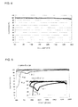
- FIG. 4 is a graph showing the reflectance of this example at wavelengths of 400 nm to 2500 nm. As is evident from FIG. 4 , the broadband reflecting mirror of this example has achieved high reflectance over the entire wavelength band of 400 nm to 2500 nm.
- FIG. 5 is a graph showing the reflectances of comparative reflecting mirrors produced by forming a Ag coating, an Al coating and a Au coating as their respective metal coatings on their glass substrates made of the same material as used in Example 1, together with the reflectance of this example.
- FIG. 5 an enlarged graph is also given in which a zone of reflectance of 80 to 100% in the above graph is shown in an enlarged manner. Note that in the enlarged graph the scale of wavelength on the abscissa axis represents that in the graph of reflectance of 0 to 100%.
- this example (Inventive Example) exhibited high reflectance of near 100% over the entire wavelength band of 400 nm to 2500 nm, but on the other hand the reflecting mirrors formed using a Ag coating, an Al coating and a Au coating, respectively, reduced their reflectance in a visible light range.
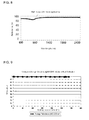
- FIG. 6 is a graph showing changes in reflectance of the broadband reflecting mirror of this example between before and after being subjected to a heat application test.
- the condition of the heat application test was to apply heat at 300°C for 264 hours.
- the reflecting mirror of this example has excellent thermal resistance.
- FIG. 7 is a graph showing the reflectances of the reflecting mirror using a Ag coating before and after heat application.
- the condition of the heat application was to apply heat at 300°C for an hour.
- the reflective mirror using a Ag coating although having high reflectance as compared to the reflecting mirrors using the other types of metal coatings as shown in FIG. 5 , can be understood to be poor in thermal resistance.
- FIG. 8 is a graph showing the reflectances of the reflecting mirror using an Al coating before and after heat application.
- the reflecting mirror using an Al coating As shown in FIG. 8 , in the reflecting mirror using an Al coating, no significant change is found between before and after the heat application, and the reflectance curves in the graph are superposed. Therefore, the reflecting mirror using an Al coating has good thermal resistance. However, as shown in FIG. 5 , the reflecting mirror has poor reflectance.
- FIG. 9 is a graph showing the thermal resistance of the broadband reflecting mirror of this example. Measured in this case were changes in average reflectance at wavelengths of 400 nm to 2500 nm with heat application time. As shown in FIG. 9 , it can be seen that the average reflectance in this example was not substantially changed even if heat application at 300°C was continued for 264 hours.
- a broadband reflecting mirror of this example is a broadband reflecting mirror exhibiting its highest reflectance when the angle of incidence thereon is approximately 16°.
- Nb 2 O 5 is used as each of first high-refractive index material layers
- SiO 2 is used as each of first low-refractive index material layers.
- TABLE 3 shows the configuration of the first reflective layered coating.
- the second reflective layered coating can have the same configuration as in Example 1. Therefore, the second reflective layered coating can have the configuration shown in TABLE 2.
- a broadband reflecting mirror of this example is a broadband reflecting mirror exhibiting its highest reflectance when the angle of incidence thereon is approximately 23°.
- Nb 2 O 5 is used as each of first high-refractive index material layers
- SiO 2 is used as each of first low-refractive index material layers.
- TABLE 4 shows the configuration of the first reflective layered coating.
- the second reflective layered coating can have the same configuration as in Example 1. Therefore, the second reflective layered coating can have the configuration shown in TABLE 2.
- a broadband reflecting mirror of this example is a broadband reflecting mirror exhibiting its highest reflectance when the angle of incidence thereon is approximately 30°.
- Nb 2 O 5 is used as each of first high-refractive index material layers
- SiO 2 is used as each of first low-refractive index material layers.
- TABLE 5 shows the configuration of the first reflective layered coating.
- the second reflective layered coating can have the same configuration as in Example 1. Therefore, the second reflective layered coating can have the configuration shown in TABLE 2.
- a broadband reflecting mirror of this example is a broadband reflecting mirror using germanium as each of second high-refractive index material layers. Since germanium has high absorption in a short wavelength band up to 2000 nm as described previously, the first reflective layered coating is designed to reflect light within a wavelength band of 400 nm to 2000 nm. On the other hand, the second reflective layered coating is designed to reflect light within a wavelength band of 2000 nm to 2500 nm.
- TABLE 6 shows the configuration of the first reflective layered coating when Nb 2 O 5 is used as each of first high-refractive index material layers and SiO 2 is used as each of first low-refractive index material layers.
- the number of layers of the first reflective layered coating is 101.
- TABLE 7 shows the configuration of the second reflective layered coating when Ge (germanium) is used as each of second high-refractive index material layers and SiO 2 (silicon oxide) is used as each of second low-refractive index material layers.
- the number of layers of the second reflective layered coating is 21.
- the total number of layers in the entire broadband reflecting mirror is 122, which is smaller than 146, the number of layers when the broadband reflecting mirror is composed only of Nb 2 O 5 and SiO 2 , but is larger than the number of layers in Example 1.
- a broadband reflecting mirror of this example is a broadband reflecting mirror in which a metal coating is provided as a third reflective coating on a second reflective layered coating.
- the mirror is a broadband reflecting mirror exhibiting its highest reflectance when the angle of reflection thereon is approximately 20°.
- the configuration of a first reflective layered coating in this example is the configuration shown in TABLE 1.
- the configuration of the second reflective layered coating and the third reflective coating in this example is the configuration shown in TABLE 8.
- the second reflective layered coating is formed by stacking a Si layer and a SiO 2 layer.
- An Al layer serving as a third reflective coating is formed on the SiO 2 layer.
- the formation of the Al layer as a third reflective coating allows the number of layers of the second reflective layered coating to be reduced as shown in TABLE 8.
- FIG. 11 is a graph showing the reflectance of this example at wavelengths of 400 nm to 2500 nm.
- the broadband reflecting mirror of this example also has achieved high reflectance over the entire wavelength band of 400 nm to 2500 nm.
- the reflectance of this example after being heated at 300°C for 264 hours is the same as in FIG. 11 and the example has excellent thermal resistance.
- a broadband reflecting mirror of this example is, like Example 6, a broadband reflecting mirror in which a metal coating is provided as a third reflective coating on a second reflective layered coating.
- the mirror is a broadband reflecting mirror exhibiting its highest reflectance when the angle of incidence thereon is approximately 20°.
- a first reflective layered coating has the configuration shown in TABLE 1.
- the second reflective layered coating and the third reflective coating has the configuration shown in TABLE 9.
- the SiO 2 layer of Layer No. 5 in TABLE 9 is a protective layer for protecting the Al coating serving as a third reflective coating. Furthermore, the SiO 2 layer of Layer No. 1 is a layer provided for improving the adhesion of the Si layer of Layer No. 2 to the glass substrate.
- the second reflective layered coating is composed of Layers Nos. 1 to 3.
- the Si layer is a second high-refractive index material layer, and the remaining SiO 2 layer is a second low-refractive index material layer.
- the provision of the Al layer as a third reflective coating allows the number of layers of the second reflective layered coating to be reduced.
- the SiO 2 layer (Layer No. 5) serving as a protective layer is provided outside of the Al layer, whereby the thermal resistance can be further enhanced.
- Example 11 The reflectance of this example at wavelengths of 400 nm to 2500 nm was as shown in FIG. 11 , which was the same as in Example 6. In addition, it has been confirmed that like Example 6 this example has excellent thermal resistance.
- FIG. 10 is a schematic diagram showing an example of a solar concentrating system.
- a plurality of heliostats 6 are placed on the ground.
- Each heliostat 6 can change the angle of its reflecting mirror according to the position of the sun to direct the reflected light of the sunlight 5 to a converging point 9.
- a light-collecting reflecting mirror 7 is provided at a high elevation short of the converging point 9.
- the light-collecting reflecting mirror 7 reflects the reflected light from the heliostat 6 to collect it to a solar collector 8 provided near the ground.
- the reflected light beams from all the heliostats 6 are directed to the light-collecting reflecting mirror 7, reflected by the light-collecting reflecting mirror 7 and then collected by the solar collector 8.
- the broadband reflecting mirror of the present invention can be used as the reflecting mirror for each heliostat 6 or as the light-collecting reflecting mirror 7. Particularly, the light-collecting reflecting mirror 7 is heated to high temperature since the reflected light beams from all the heliostats 6 are collected thereto. Therefore, the light-collecting reflecting mirror 7 is required to have high thermal resistance. Accordingly, the broadband reflecting mirror of the present invention can be suitably used as such a light-collecting reflecting mirror.
Landscapes
- Engineering & Computer Science (AREA)
- Physics & Mathematics (AREA)
- Sustainable Energy (AREA)
- Life Sciences & Earth Sciences (AREA)
- Optics & Photonics (AREA)
- Sustainable Development (AREA)
- General Physics & Mathematics (AREA)
- Thermal Sciences (AREA)
- Chemical & Material Sciences (AREA)
- Combustion & Propulsion (AREA)
- Mechanical Engineering (AREA)
- General Engineering & Computer Science (AREA)
- Optical Elements Other Than Lenses (AREA)
- Optical Filters (AREA)
Applications Claiming Priority (3)
| Application Number | Priority Date | Filing Date | Title |
|---|---|---|---|
| JP2008193505 | 2008-07-28 | ||
| JP2009092807A JP5229075B2 (ja) | 2008-07-28 | 2009-04-07 | 広帯域反射鏡 |
| PCT/JP2009/003014 WO2010013389A1 (ja) | 2008-07-28 | 2009-06-30 | 広帯域反射鏡 |
Publications (2)
| Publication Number | Publication Date |
|---|---|
| EP2320253A1 true EP2320253A1 (de) | 2011-05-11 |
| EP2320253A4 EP2320253A4 (de) | 2013-06-05 |
Family
ID=41610105
Family Applications (1)
| Application Number | Title | Priority Date | Filing Date |
|---|---|---|---|
| EP09802639.6A Withdrawn EP2320253A4 (de) | 2008-07-28 | 2009-06-30 | Breitbandreflexionsspiegel |
Country Status (7)
| Country | Link |
|---|---|
| US (1) | US20110096391A1 (de) |
| EP (1) | EP2320253A4 (de) |
| JP (1) | JP5229075B2 (de) |
| CN (1) | CN102112897B (de) |
| AU (1) | AU2009277894B2 (de) |
| IL (1) | IL209882A0 (de) |
| WO (1) | WO2010013389A1 (de) |
Cited By (1)
| Publication number | Priority date | Publication date | Assignee | Title |
|---|---|---|---|---|
| WO2016044212A1 (en) * | 2014-09-17 | 2016-03-24 | Corning Incorporated | High-efficiency multiwavelength beam expander employing dielectric-enhanced mirrors |
Families Citing this family (34)
| Publication number | Priority date | Publication date | Assignee | Title |
|---|---|---|---|---|
| CN101872271B (zh) * | 2009-04-27 | 2013-04-24 | 鸿富锦精密工业(深圳)有限公司 | 触控系统 |
| JP2014038118A (ja) * | 2010-12-09 | 2014-02-27 | Asahi Glass Co Ltd | 反射鏡およびその製造方法 |
| CN102540310B (zh) * | 2010-12-13 | 2015-07-01 | 鸿富锦精密工业(深圳)有限公司 | 双色镜、阳光收集装置及太阳能装置 |
| CN103443559A (zh) * | 2011-03-17 | 2013-12-11 | 冯·阿德纳设备有限公司 | 用于太阳能应用的反射层系统及其制造方法 |
| CN104081229B (zh) * | 2012-02-08 | 2016-10-19 | 东海光学株式会社 | 光学制品及其制造方法 |
| TWI545354B (zh) * | 2012-05-02 | 2016-08-11 | 鴻海精密工業股份有限公司 | 紫外截止濾光片及鏡頭模組 |
| CN102681054B (zh) * | 2012-05-08 | 2014-03-19 | 太原理工大学 | 基于光子晶体的全可见光波段全角度反射器 |
| JP2014047952A (ja) * | 2012-08-30 | 2014-03-17 | Babcock-Hitachi Co Ltd | 太陽熱集熱システムおよびその運用方法、太陽熱集熱システムを備えた発電プラント |
| CN203240804U (zh) * | 2012-09-27 | 2013-10-16 | 西门子聚集太阳能有限公司 | 玻璃管、吸热管和抛物槽收集器 |
| US9261634B2 (en) | 2013-01-29 | 2016-02-16 | Viavi Solutions Inc. | Variable optical filter and a wavelength-selective sensor based thereon |
| JP2014154589A (ja) * | 2013-02-05 | 2014-08-25 | Fujifilm Corp | 太陽光集光用反射鏡 |
| US9977157B2 (en) * | 2013-02-13 | 2018-05-22 | Guardian Europe S.à r.l. | Dielectric mirror |
| US9594195B2 (en) | 2013-02-13 | 2017-03-14 | Centre Luxembourgeois de Recherches Pour le Verre et la Ceramique (CRVC) SaRL | Dielectric mirror |
| JP2014191230A (ja) * | 2013-03-27 | 2014-10-06 | Fujifilm Corp | 太陽光集光用フィルムミラー |
| JP5597780B1 (ja) * | 2014-02-26 | 2014-10-01 | セラテックジャパン株式会社 | 近赤外線カットフィルタ及びその製造方法並びにそれを備えた眼鏡 |
| US9910200B1 (en) * | 2014-05-05 | 2018-03-06 | The United States Of America As Represented By The Secretary Of The United States | Increased visible and infrared transmission through radio frequency EMI shields |
| CN104459848A (zh) * | 2014-11-27 | 2015-03-25 | 中国科学院长春光学精密机械与物理研究所 | 基于氧化铝中间层的铝银多层宽带反射膜 |
| JP2016161707A (ja) * | 2015-02-27 | 2016-09-05 | オリンパス株式会社 | 反射ミラー、及び、顕微鏡 |
| CN104698519B (zh) * | 2015-03-27 | 2017-04-19 | 中国科学院国家授时中心 | 一种低热噪声高反射光学复合膜结构及其制备方法 |
| CN105137515A (zh) * | 2015-09-11 | 2015-12-09 | 中国科学院长春光学精密机械与物理研究所 | 一种日盲反射式介质滤光片及其制备方法 |
| CN105842758B (zh) * | 2016-05-13 | 2017-11-07 | 中国科学院宁波材料技术与工程研究所 | 具有叠层结构的耐腐蚀高反光的正面镜及其制备方法 |
| CN106324740B (zh) * | 2016-11-16 | 2018-12-18 | 天津津航技术物理研究所 | 一种宽带吸收薄膜及其制备方法 |
| CN106443848A (zh) * | 2016-11-16 | 2017-02-22 | 天津津航技术物理研究所 | 一种宽带激光薄膜反射镜 |
| JP2020046445A (ja) * | 2017-01-18 | 2020-03-26 | Agc株式会社 | Cspミラー、およびcspミラー用の膜付きガラス基板の製造方法 |
| CN106873181B (zh) * | 2017-04-21 | 2023-06-16 | 严爱霞 | 一种医用射线防护眼镜镜片及其制作工艺 |
| US11143800B2 (en) * | 2017-06-16 | 2021-10-12 | Corning Incorporated | Extending the reflection bandwith of silver coating stacks for highly reflective mirrors |
| JP6748150B2 (ja) * | 2018-06-14 | 2020-08-26 | ファナック株式会社 | ガルバノミラー及びレーザ加工装置 |
| CN110737036A (zh) | 2018-07-18 | 2020-01-31 | 福州高意光学有限公司 | 宽角度应用高反射镜 |
| CN109239820A (zh) * | 2018-10-19 | 2019-01-18 | 布勒莱宝光学设备(北京)有限公司 | 可透光用于植物生长的聚光太阳能反射镜 |
| CN109799557A (zh) * | 2019-02-28 | 2019-05-24 | 南京前海有芯信息技术有限公司 | 一种能反射紫外光的薄膜 |
| TWI884885B (zh) | 2019-04-15 | 2025-05-21 | 以色列商魯姆斯有限公司 | 製造光導光學元件的方法 |
| CN110119005A (zh) * | 2019-05-28 | 2019-08-13 | 苏州大学 | 一种宽波段反射镜 |
| KR20230019854A (ko) * | 2020-06-12 | 2023-02-09 | 닛토덴코 가부시키가이샤 | 필름 미러 적층체 및 미러 부재 |
| US12278255B2 (en) | 2021-06-11 | 2025-04-15 | Raytheon Company | Thin film obscurant for microelectronics |
Family Cites Families (22)
| Publication number | Priority date | Publication date | Assignee | Title |
|---|---|---|---|---|
| JPS574003A (en) | 1980-06-11 | 1982-01-09 | Toshiba Electric Equip Corp | Solar energy absorber |
| US4746202A (en) * | 1985-07-11 | 1988-05-24 | Coherent, Inc. | Polarization preserving reflector and method |
| JPS6257904A (ja) | 1985-09-06 | 1987-03-13 | 株式会社 吉利 | シヨ−ル |
| JPS63179302A (ja) * | 1987-01-21 | 1988-07-23 | Mitsubishi Electric Corp | 広帯域反射ミラ− |
| JPH0786568B2 (ja) * | 1987-03-25 | 1995-09-20 | 東芝ライテック株式会社 | 光源装置 |
| JPH0758355A (ja) * | 1993-05-12 | 1995-03-03 | Optical Coating Lab Inc | Uv/ir反射太陽電池カバー |
| JPH075311A (ja) * | 1993-06-15 | 1995-01-10 | Sony Corp | 光学ミラー装置 |
| IL108506A (en) * | 1994-02-01 | 1997-06-10 | Yeda Res & Dev | Solar energy plant |
| US5688608A (en) * | 1994-02-10 | 1997-11-18 | Industrial Technology Research Institute | High refractive-index IR transparent window with hard, durable and antireflective coating |
| JPH07280999A (ja) * | 1994-04-12 | 1995-10-27 | Nikon Corp | X線多層膜反射鏡 |
| JP2951297B2 (ja) * | 1997-10-15 | 1999-09-20 | 三鷹光器株式会社 | 太陽光集光システム |
| US6926952B1 (en) * | 1998-01-13 | 2005-08-09 | 3M Innovative Properties Company | Anti-reflective polymer constructions and method for producing same |
| JP3976919B2 (ja) * | 1998-12-28 | 2007-09-19 | 日東光器株式会社 | 反射ミラー |
| WO2001086328A1 (en) * | 2000-05-10 | 2001-11-15 | Oyokoden Lab Co., Ltd. | Optical component and dispersion compensating method |
| CN100575418C (zh) * | 2001-03-21 | 2009-12-30 | Hoya株式会社 | 透明成形体及其制造方法 |
| JP2003302520A (ja) * | 2002-04-10 | 2003-10-24 | Sumitomo Electric Ind Ltd | 赤外レーザ用反射ミラーとその製造方法 |
| WO2005019881A1 (en) * | 2003-08-12 | 2005-03-03 | Massachusetts Institute Of Technology | Process for fabrication of high reflectors by reversal of layer sequence and application thereof |
| US7206125B2 (en) * | 2003-11-10 | 2007-04-17 | Therma-Wave, Inc. | Infrared blocking filter for broadband Optical metrology |
| CN100468081C (zh) * | 2005-06-03 | 2009-03-11 | 鸿富锦精密工业(深圳)有限公司 | 光学元件 |
| JP2007133325A (ja) * | 2005-11-14 | 2007-05-31 | Fujinon Sano Kk | 反射ミラー及び光ピックアップ |
| JP2007183525A (ja) * | 2005-12-07 | 2007-07-19 | Murakami Corp | 誘電体多層膜フィルタ |
| CN101743490A (zh) * | 2008-07-07 | 2010-06-16 | 柯尼卡美能达精密光学株式会社 | 反射镜结构体 |
-
2009
- 2009-04-07 JP JP2009092807A patent/JP5229075B2/ja not_active Expired - Fee Related
- 2009-06-30 AU AU2009277894A patent/AU2009277894B2/en not_active Ceased
- 2009-06-30 EP EP09802639.6A patent/EP2320253A4/de not_active Withdrawn
- 2009-06-30 WO PCT/JP2009/003014 patent/WO2010013389A1/ja not_active Ceased
- 2009-06-30 US US12/997,612 patent/US20110096391A1/en not_active Abandoned
- 2009-06-30 CN CN2009801298744A patent/CN102112897B/zh not_active Expired - Fee Related
-
2010
- 2010-12-09 IL IL209882A patent/IL209882A0/en unknown
Cited By (3)
| Publication number | Priority date | Publication date | Assignee | Title |
|---|---|---|---|---|
| WO2016044212A1 (en) * | 2014-09-17 | 2016-03-24 | Corning Incorporated | High-efficiency multiwavelength beam expander employing dielectric-enhanced mirrors |
| US10502965B2 (en) | 2014-09-17 | 2019-12-10 | Corning Incorporated | High-efficiency multiwavelength beam expander employing dielectric-enhanced mirrors |
| US11092814B2 (en) | 2014-09-17 | 2021-08-17 | Corning Incorporated | High-efficiency multiwavelength beam expander employing dielectric-enhanced mirrors |
Also Published As
| Publication number | Publication date |
|---|---|
| AU2009277894B2 (en) | 2014-06-05 |
| JP2010055058A (ja) | 2010-03-11 |
| WO2010013389A1 (ja) | 2010-02-04 |
| US20110096391A1 (en) | 2011-04-28 |
| CN102112897B (zh) | 2013-02-13 |
| CN102112897A (zh) | 2011-06-29 |
| AU2009277894A1 (en) | 2010-02-04 |
| JP5229075B2 (ja) | 2013-07-03 |
| IL209882A0 (en) | 2011-02-28 |
| EP2320253A4 (de) | 2013-06-05 |
Similar Documents
| Publication | Publication Date | Title |
|---|---|---|
| EP2320253A1 (de) | Breitbandreflexionsspiegel | |
| US20130342900A1 (en) | Reflection layer system for solar applications and method for the production thereof | |
| US7833629B2 (en) | Transparent substrate comprising an antireflection coating | |
| KR101194257B1 (ko) | 광대역 반사방지 다층코팅을 갖는 태양전지용 투명 기판 및 그 제조방법 | |
| KR20080089351A (ko) | 반사방지 코팅을 구비한 투명한 기판 | |
| KR101788368B1 (ko) | 저방사 코팅막, 이의 제조방법 및 이를 포함하는 창호용 기능성 건축 자재 | |
| JP2002254550A (ja) | 複合材料 | |
| KR101788369B1 (ko) | 저방사 코팅막, 이의 제조방법 및 이를 포함하는 창호용 기능성 건축 자재 | |
| CN103884122B (zh) | 一种太阳能光热转换集热器透明热镜及其制备方法 | |
| JP4565105B2 (ja) | 太陽電池用の光学薄膜およびその製造方法 | |
| US20160003498A1 (en) | Selective Solar Absorber Having a Thick Corrosion-Resistant Passivation and Thermal Barrier Layer for High Temperature Applications and its Process of Preparation | |
| CN115451594B (zh) | 一种宽光谱太阳能吸收增强器件及其制备方法 | |
| US9970684B2 (en) | Optical selective film | |
| KR101194258B1 (ko) | 광대역 반사방지 다층코팅을 갖는 태양전지용 투명 기판 및 그 제조방법 | |
| KR101688408B1 (ko) | 태양전지 모듈의 후면 반사용으로 유용한 고반사성 및 고내구성 다층코팅 기판 및 그 제조방법 | |
| KR101456220B1 (ko) | 반사방지 코팅층을 가지는 투명기판 및 그 제조방법 | |
| CN109324362B (zh) | 一种聚光反射镜及制备方法 | |
| CN108802985A (zh) | 一种柔性聚光反射镜 | |
| CN115425149A (zh) | 一种热稳定的钙钛矿太阳能电池结构及其制备方法 | |
| CN223816116U (zh) | 一种太阳能综合利用系统及设有该系统的光热电站 | |
| KR101700246B1 (ko) | 태양전지 모듈의 후면 반사용 다층코팅 기판 및 그 제조방법 | |
| JPH09175840A (ja) | 太陽電池用低反射ガラス基板 | |
| JPH09197101A (ja) | プラスチック製光学部品の反射防止膜 | |
| Martirosyan et al. | Reflectance calculation of a diamond-like carbon/porous Si thin films in silicon-based photovoltaic cells | |
| CN121741914A (zh) | 一种耐候型hud滤光反射镜及其制备方法 |
Legal Events
| Date | Code | Title | Description |
|---|---|---|---|
| PUAI | Public reference made under article 153(3) epc to a published international application that has entered the european phase |
Free format text: ORIGINAL CODE: 0009012 |
|
| 17P | Request for examination filed |
Effective date: 20101221 |
|
| AK | Designated contracting states |
Kind code of ref document: A1 Designated state(s): AT BE BG CH CY CZ DE DK EE ES FI FR GB GR HR HU IE IS IT LI LT LU LV MC MK MT NL NO PL PT RO SE SI SK TR |
|
| AX | Request for extension of the european patent |
Extension state: AL BA RS |
|
| DAX | Request for extension of the european patent (deleted) | ||
| A4 | Supplementary search report drawn up and despatched |
Effective date: 20130508 |
|
| RIC1 | Information provided on ipc code assigned before grant |
Ipc: F24J 2/10 20060101ALI20130502BHEP Ipc: G02B 5/28 20060101ALI20130502BHEP Ipc: F24J 2/18 20060101ALN20130502BHEP Ipc: G02B 5/08 20060101AFI20130502BHEP Ipc: F24J 2/16 20060101ALN20130502BHEP Ipc: G02B 5/26 20060101ALI20130502BHEP |
|
| STAA | Information on the status of an ep patent application or granted ep patent |
Free format text: STATUS: THE APPLICATION IS DEEMED TO BE WITHDRAWN |
|
| 18D | Application deemed to be withdrawn |
Effective date: 20160105 |