EP2323252A1 - Magneto-resistiver Hochfrequenzoszillator - Google Patents
Magneto-resistiver Hochfrequenzoszillator Download PDFInfo
- Publication number
- EP2323252A1 EP2323252A1 EP10189958A EP10189958A EP2323252A1 EP 2323252 A1 EP2323252 A1 EP 2323252A1 EP 10189958 A EP10189958 A EP 10189958A EP 10189958 A EP10189958 A EP 10189958A EP 2323252 A1 EP2323252 A1 EP 2323252A1
- Authority
- EP
- European Patent Office
- Prior art keywords
- ferromagnetic
- layer
- ferrimagnetic
- layers
- magnetic
- Prior art date
- Legal status (The legal status is an assumption and is not a legal conclusion. Google has not performed a legal analysis and makes no representation as to the accuracy of the status listed.)
- Withdrawn
Links
Images

Classifications
-
- H—ELECTRICITY
- H03—ELECTRONIC CIRCUITRY
- H03B—GENERATION OF OSCILLATIONS, DIRECTLY OR BY FREQUENCY-CHANGING, BY CIRCUITS EMPLOYING ACTIVE ELEMENTS WHICH OPERATE IN A NON-SWITCHING MANNER; GENERATION OF NOISE BY SUCH CIRCUITS
- H03B15/00—Generation of oscillations using galvano-magnetic devices, e.g. Hall-effect devices, or using superconductivity effects
- H03B15/006—Generation of oscillations using galvano-magnetic devices, e.g. Hall-effect devices, or using superconductivity effects using spin transfer effects or giant magnetoresistance
-
- G—PHYSICS
- G11—INFORMATION STORAGE
- G11C—STATIC STORES
- G11C11/00—Digital stores characterised by the use of particular electric or magnetic storage elements; Storage elements therefor
- G11C11/02—Digital stores characterised by the use of particular electric or magnetic storage elements; Storage elements therefor using magnetic elements
- G11C11/16—Digital stores characterised by the use of particular electric or magnetic storage elements; Storage elements therefor using magnetic elements using elements in which the storage effect is based on magnetic spin effect
- G11C11/161—Digital stores characterised by the use of particular electric or magnetic storage elements; Storage elements therefor using magnetic elements using elements in which the storage effect is based on magnetic spin effect details concerning the memory cell structure, e.g. the layers of the ferromagnetic memory cell
-
- H—ELECTRICITY
- H10—SEMICONDUCTOR DEVICES; ELECTRIC SOLID-STATE DEVICES NOT OTHERWISE PROVIDED FOR
- H10N—ELECTRIC SOLID-STATE DEVICES NOT OTHERWISE PROVIDED FOR
- H10N50/00—Galvanomagnetic devices
- H10N50/10—Magnetoresistive devices
Definitions
- the invention relates to a radio frequency oscillator.
- the invention relates to a radio frequency oscillator incorporating a magnetoresistive device in which circulates a spin-polarized electric current.
- the passage of the current causes a periodic variation in the resistance of the magnetoresistive device.
- a high frequency signal that is to say whose frequency is typically between 100 MHz and a few tens of GHz, is built from this periodic variation.
- the period of the variations of the resistivity, and therefore the frequency of oscillation can be adjusted by varying the intensity of the current flowing through the magnetoresistive device and / or the external magnetic field.
- oscillators for example, are intended to be used in the field of radio telecommunications because they can generate a wide range of frequencies with a high quality factor.
- radiofrequency oscillators are derived from spin electronics.
- This spin polarization of the current is at the origin of magnetoresistive phenomena in magnetic multilayers such as giant magnetoresistance ( Baibich, M., Broto, JM, Fert, A., Nguyen Van Dau, F., Petroff, F., Etienne, P., Creuzet, G., Friederch, A. and Chazelas, J., "Giant magnetoresistance of (001) Fe / (001) Cr magnetic superlattices ", Phys.Rev.Lett., 61 (1988) 2472 ), or tunnel magnetoresistance ( Moodera, JS., Kinder, LR., Wong, TM. and Meservey, R. "Large magnetoresistance at room temperature in ferromagnetic thin film tunnel junctions", Phys.Rev.Lett 74, (1995) 3273-6 ).
- the polarized current can also generate sustained magnetic excitations, also called oscillations ( Kiselev, SI, Sankey, JC, Krivorotov, LN., Emley, NC, Schoelkopf, RJ, Buhrman, RA, and Ralph, DC, "Microwave oscillations of a nanomagnet driven by a spin-polarized current," Nature, 425, 380 (2003 )).
- the use of the magnetic excitation generation effect maintained in a magnetoresistive device makes it possible to convert this effect into an electrical resistance modulation which can be used directly in the electronic circuits, and thus, as a corollary, capable of intervening directly at the frequency level.
- the document US 5,695,864 describes various developments implementing the physical principle mentioned above. In particular, it describes the precession of the magnetization of a magnetic layer traversed by a spin polarized electric current. The physical principles used and the terminology used are also described and defined in the patent application. FR 2,892,871 .
- the oscillation frequency of these radiofrequency oscillators is adjusted by varying the intensity of the current flowing through it and possibly also on an external magnetic field.
- Requirement FR 2,892,871 teaches that to improve the precession coherence it is advantageous to make the free layer using a stack of ferromagnetic sublayers constituting a synthetic antiferromagnet.
- coherence of the precession it is meant that the magnetization is set in motion as a single block over the entire extension of the current layer passing through the structure (that is to say on the section of the pillar in the pillar geometry and on the section of the current cone at the level of the free layer in the case of the nanocontact geometry), as opposed to generating multiple small incoherent excitations between them.
- synthetic antiferromagnetism also known by the acronym SAF (synthetic antiferromagnetic)
- SAF synthetic antiferromagnetic
- ferromagnetic sublayers of a synthetic antiferromagnet are dimensioned so that the overall magnetization of the synthetic antiferromagnetic is zero in the absence of an external magnetic field.
- the ferromagnetic sublayers are separated from each other by thin non-magnetic sub-layers.
- the thickness of the non-magnetic sub-layer or layers is systematically chosen to obtain antiferromagnetic RKKY coupling.
- a synthetic antiferromagnetic is a particular synthetic ferrimagnetic. Synthetic ferrimagnetics are known by the acronym SYF (Synthetic Ferrimagnetic).
- SYF Synthetic Ferrimagnetic
- a synthetic ferrimagnetic is a stack of at least two ferromagnetic or ferrimagnetic sub-layers, coupled to each other through a non-magnetic layer by RKKY coupling antiferromagnetic. Unlike the synthetic antiferromagnetic, the resulting magnetization of this stack is not necessarily zero.
- layer or nonmagnetic material is meant a layer or material which does not exhibit measurable magnetization in zero field. It can therefore be a material having no magnetic property, a non-magnetic material or a diamagnetic material or a paramagnetic material.
- the patent application FR 2,892,871 discloses the use of a synthetic antiferromagnetic to form the free layer of the radio frequency oscillator.
- This synthetic antiferromagnetic consists solely of two ferromagnetic sublayers.
- the aim of the invention is to propose a radio frequency oscillator having an improved quality factor. It therefore relates to a radio frequency oscillator in which the free layer and / or the reference layer is formed of a stack of at least three ferromagnetic or ferrimagnetic sublayers coupled to each other by coupling RKKY (Ruderman-Kittel- Kasuya-Yosida) and among which at least two sublayers are magnetically coupled to one another by an antiferromagnetic RKKY coupling.
- RKKY Rel-Kittel- Kasuya-Yosida
- the line width ⁇ f of the radio frequency oscillator at the oscillation frequency f is inversely proportional to the volume (hereinafter called the effective volume and denoted by V eff ) of the magnetic material of the free layer or of the layer. reference.
- V eff volume of the magnetic material of the free layer or of the layer. reference.
- the effective volume of the free or reference layer corresponds to the sum of the volumes of each ferromagnetic or ferrimagnetic sub-layer that composes it. This increase in the effective volume decreases the linewidth ⁇ f and thus improves the quality factor of this oscillator.
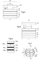
- the figure 1 represents a radiofrequency oscillator 2.
- This oscillator 2 integrates a magnetoresistive device in which circulates a spin-polarized electric current.
- This magnetoresistive device is shaped according to a geometry known by the acronym CPP ("current perpendicular to plane"). More specifically, on the figure 1 , the magnetoresistive device adopts a structure known as the "nanopillar".
- This nanopillar is a pillar formed by stacking horizontal layers of the same horizontal section one above the other.
- the oscillator 2 comprises at each end of the pillar a conductive electrode, respectively, 4 and 6. These electrodes make it possible to bring the current which passes through the various layers forming the magnetoresistive device perpendicular to the plane of these layers. When the intensity of this current exceeds the intensity of the critical current I c , the voltage between these electrodes 4 and 6 oscillates at a frequency which is a function of the current flowing through the electrodes. For example, this voltage is transmitted to an electronic equipment 7 which processes it to, for example, create a reference signal.
- the pillar mainly comprises three layers, namely a reference layer 8, a free layer 10 and a non-magnetic layer 12 interposed between the layers 8 and 10.
- the non-magnetic layer is better known by the term 'Spacer' or 'spacer' in English.
- These layers 8, 10 and 12 are arranged and shaped so as to allow the appearance of the magnetoresistive properties, that is to say a variation of the resistance of the pillar as a function of the magnetization directions of the layers 8 and 10.
- the width L of the various layers that make up the pillar is constant.
- the width L is less than 1 ⁇ m and, typically, between 20 nm and 200 nm.
- the reference layer 8 is made of an electrically conductive magnetic material. Its upper face is directly in contact with the spacer 12. It has a direction of easier magnetization included in the plane of the layer.
- the reference layer 8 has the function of spin polarizing the electrons of the current flowing through it. It therefore has a thickness sufficient to achieve this function. Typically, the thickness of the reference layer 8 is strictly greater than the spin diffusion length (see, for example, the patent application FR2892871 for a definition of this term).
- the reference layer 8 is made of cobalt (Co), nickel (Ni), iron (Fe) or their alloy (CoFe, NiFe, CoFeB, etc.).
- the thickness of the reference layer 8 is of the order of a few nanometers.
- the reference layer 8 can be laminated by inserting a few (typically 2 to 4) very thin copper, silver or gold layers of the order of 0.2 to 0.5 nm to reduce the spin diffusion length. It is also possible that the layer 8 is a SyF or a SAF. To improve the readability of the figure 1 , the proportionality between the thickness of the different layers has not been preserved.
- the reference layer 8 has a magnetization whose direction is fixed.
- fixed direction magnetization it is meant that the direction of the magnetic moment of the reference layer 8 is more difficult to modify than the direction of the magnetic moment of the free layer 10.
- the magnetization of the reference 8 is for example trapped by a conductive antiferromagnetic layer 16 interposed between the reference layer 8 and the electrode 6.
- the upper face of the layer 16 is for example directly in contact with the lower face of the reference layer 8.
- the thickness of the layer 16 is between 5 and 50 nm. It may be made of a manganese alloy such as one of the following alloys IrMn, PtMn, FeMn, etc.
- this layer 16 is made of a material selected from the group consisting of IrMn, FeMn, PtMn, NiMn.
- the spacer 12 is a non-magnetic layer. This spacer 12 is sufficiently fine to allow the spin polarized current to pass from the reference layer 8 to the free layer 10 by limiting the loss of polarization. Conversely, the thickness of this spacer 12 is sufficiently large to ensure the magnetic decoupling between the layers 8 and 10.
- the spacer 12 is made of an electrically conductive material such as copper (Cu).
- the magnetoresistive properties of the pillar are then called giant magnetoresistance or GMR (Geant Magnetoresistance).
- GMR Giant Magnetoresistance
- the thickness of the spacer 12 is typically greater than 2 nm. Generally, its thickness is between 2 and 40 nm and preferably equal to 5 nm to ⁇ 25%.
- the spacer 12 may also be made of an insulating material such as aluminum oxide or nitride, magnesium oxide, tantalum nitride, strontium titanate (SrTiO 3 ), etc.
- the pillar then has tunnel magnetoresistive properties or TMR (Tunnel Magnetoresistance).
- TMR Tunnel Magnetoresistive properties
- the thickness of the spacer 12 is typically between 0.5 nm and 3 nm.
- the free layer 10 is an electrically conductive magnetic layer whose magnetization can more easily rotate or "precess" than that of the reference layer 8.
- this free layer 10 is made by stacking three ferromagnetic sub-layers 20 to 21.
- the sub-layers 20, 21 and 21, 22 are coupled to each other by an antiferromagnetic RKKY coupling.
- the stack of sublayers 20 to 22 thus constitutes a synthetic ferrimagnetic.
- the direction of easier magnetization of these sublayers is included in the plane of the underlays.
- the underside of the underlayer 20 is directly in contact with the upper face of the spacer 12.
- the thickness t 1 of the underlayer 20 is as small as possible. Indeed, the more this thickness t 1 is reduced, the smaller the critical current I c is.
- the thickness t 1 is between 1 nm and 6 nm and preferably between 1 nm and 4 nm.
- This underlayer 20 is made of a ferromagnetic material such as cobalt, nickel or iron or an alloy of these different metals (for example CoFe, CoFeB, NiFe, etc.).
- the overall magnetic moment of the sublayer 20 is oriented parallel to the plane of this sublayer.
- the direction of this magnetic moment is represented by an arrow 24 on the figure 1 .
- the amplitude of the magnetic moment of the sublayer 20 is proportional to the magnetization M 1 of the ferromagnetic material used for this sublayer multiplied by the thickness t 1 .
- the sub-layer 20 occupies a volume V 1 .
- the magnetic moment m is equal to the product of the magnetization M 1 by this volume V 1 and therefore proportional to the product M 1 * t 1 .
- a non-magnetic conductive sub-layer 26 is directly interposed between these two sub-layers 20 and 21.
- the thickness of this sublayer 26 is sufficiently fine for the Ferromagnetic sublayers 20 and 21 are antiferromagnetically coupled. By antiferromagnetic coupling it is indicated that the magnetic moments of the sublayers 20 and 21 are antiparallel.
- the underlayer 26 is made of a material such as ruthenium (Ru), rhenium (Re), copper (Cu), chromium (Cr), platinum (Pt) or silver ( Ag).
- ruthenium Ru
- rhenium Re
- Cu copper
- Cr chromium
- platinum Pt
- Ag silver
- its thickness to obtain an RKKY coupling is not the same.
- the underlayer 26 is chromium, the thickness is less than or equal to 4.5 nm. If the underlayer 26 is copper, the thickness is less than 1.5 nm.
- the thickness of the underlayer 26 is a few angstroms, that is to say between 1 and 50 angstroms.
- the thickness here is 8 angstroms.
- the underside of the underlayer 21 is directly deposited on the underlayer 26.
- This sublayer 21 is magnetically coupled by antiferromagnetic RKKY coupling at the same time to the sub-layers 20 and 22.
- the direction of its magnetic moment, represented by an arrow 28, is therefore opposed to that of the magnetic moment of the sub-layers 20 and 22.
- the thickness t 2 of the sublayer 21 is chosen strictly greater than the thickness t 1 so as to further increase the effective volume V eff of the free layer 10. In fact, the higher the volume effective V eff of the free layer 10 increases the line width ⁇ f decreases.
- the thickness t 2 is chosen so that the volume V 2 of the underlayer 21 is at least 10 or even more than 25% greater than the volume V 1 of the underlayer 20.
- the underlayer 21 is designed to cancel the magnetic moments of the sub-layers 20 and 22 so as to achieve a synthetic antiferromagnetic.
- the use of a compensated synthetic antiferromagnetic to produce the free layer 10 makes it possible to increase the stability of the oscillator by reducing the dipolar field radiated on the other magnetic layers.
- the underlayer 21 is made of the same ferromagnetic material as the sub-layers 20 and 22. Its magnetic moment is therefore proportional to the magnetization M 1 multiplied by the thickness t 2 . Therefore, to cancel the magnetic moments of the sub-layers 20 and 22, the thickness t 2 is chosen to be twice the thickness t 1 .
- a conductive non-magnetic sub-layer 30 is interposed between the sub-layers 21 and 22 so as to obtain the antiferromagnetic RKKY coupling between these sub-layers.
- this sublayer 30 is identical to the sublayer 26.
- the underside of the underlayer 22 is directly in contact with the upper face of the underlayer 30.
- the underlayer 22 is for example identical to the underlayer 20.
- the direction of its magnetic moment is here represented by an arrow 32.
- the figure 2 represents a radio frequency oscillator 40 identical to the radiofrequency oscillator 2 except that a layer 44 of antiferromagnetic material is deposited on the free layer 10.
- the layer 44 is therefore interposed between the electrode 4 on one side and on the other side the free layer 10.
- this layer 44 is made of a material identical to those used for the layer 16.
- This layer 44 alters the relative freedom of the magnetization of the free layer 10.
- playing on the thickness of this layer 44 it can be ensured that the magnetic coupling used is less important than that used between the reference layer 8 and the antiferromagnetic layer 16.
- the magnetization of the layer free 10 nevertheless comes to precess and the The coupling inherent in the antiferromagnetic layer 44 contributes to maintaining the coherence of this magnetization.
- the figure 3 represents a radio frequency oscillator 50 identical to that of the figure 2 with the exception that the layer 44 is replaced by a polarizer 52 separated from the free layer 10 by a spacer 54.
- a polarizer is a magnetic layer or multilayer whose magnetization is outside the plane of the layer and, preferably, perpendicular to the plane of the layer. The polarizer is used to spin polarize the current flowing through it.
- the polarizer is composed of several sub-layers superimposed on each other, for example an alternation of magnetic and metallic layers (for example (Co / Pt) n).
- the polarizer is not described in more detail. For more information on polarizers, it is possible to refer to the patent application FR2 817 998 .
- the polarizer 52 is directly deposited under the electrode 4.
- the magnetic moment of this polarizer is perpendicular to the plane of the layers.
- the spacer 54 is directly deposited under the polarizer 52. This spacer performs the same functions as the spacer 12.
- the presence of the polarizer makes it possible to obtain a precession of the magnetization of the free layer 10 outside its plane. This allows for example to operate this oscillator in zero field, that is to say in the absence of external magnetic field.
- the figure 4 represents a radio frequency oscillator 60 whose quality factor is improved by using the same teaching as that given with respect to the figure 1 .
- the oscillator 60 is made according to a structure known as nanocontact or "point-contact" stacking. Such structures are described in the patent application FR 2,892,871 . It will not be described here in detail.
- Oscillator 60 is identical to oscillator 2 with the exception that electrode 4 is replaced by electrode 62.
- the electrode 6 and the layers 8, 10, 12 and 16 have the same horizontal section of width L.
- This width L is typically greater than 100 nm. It can reach several microns.
- the electrode 62 has a tip 64 of width Lp directly in contact with the upper face of the free layer 10.
- the width Lp is strictly smaller than the width L, so that the electrons of the current flowing between the electrodes 4 and 6 essentially distribute in a cone in the stack of layers 8, 10, 12 and 16.
- the width Lp is several times smaller (for example five times smaller) than the width L.
- the width Lp is between a few nanometers and 20 nm or 200 nm.
- the figure 5 represents an oscillator 70 identical to the oscillator 60 except that the electrode 62 is replaced by an electrode 72 superimposed on a polarizer 74 and a spacer 76.
- the polarizer 72 and the spacer 74 are identical, respectively to the polarizer 52 and the spacer 54 except that their width Lp is several times smaller than the width L of the layers 8, 10 and 12.
- the ratio between the width Lp and the width L is identical to that described with respect to the figure 4 .
- their width Lp is identical to that of the tip 64.
- the radio frequency oscillator is possible.
- the previous embodiments are described in the particular case where the free layer is made using a synthetic antiferromagnetic three ferromagnetic sublayers.
- the ferromagnetic sublayers it is not necessary that the ferromagnetic sublayers be dimensioned so that their magnetic moment compensate each other.
- the stack of sub-layers can simply form a synthetic ferrimagnetic.
- the thickness of the sub-layer NM i is able to create an antiferromagnetic RKKY coupling between the sub-layers FM i and FM i + 1 .
- the figure 7 represents a stack 90 of four ferromagnetic sub-layers 92 to 95 between which are interposed non-magnetic sub-layers 98 to 100.
- the thickness of the sub-layer 98 is chosen so that the sub-layers 92 and 93 are magnetically coupled. by a ferromagnetic RKKY coupling.
- the thickness of the underlayer 100 is chosen to obtain a ferromagnetic RKKY coupling between the sub-layers 94 and 95.
- the thickness of the underlayer 99 is chosen to perform antiferromagnetic RKKY coupling between underlayments 93 and 94.
- the direction of the magnetic moment of each ferromagnetic sublayer is represented by an arrow located in the corresponding sublayer. The curved arrows shown on the outside of the stack illustrate the direction of some lines of magnetic fields.
- the stack 90 is compensated, that is to say that it is made in such a way that its overall magnetic moment is equal to zero. For this, it is possible to play on the volume of each ferromagnetic sublayer.
- the improvement of the quality factor of the radio frequency oscillator also occurs if the reference layer is produced using a synthetic ferrimagnetic or a stack of at least three ferromagnetic sublayers coupled by coupling RKKY such That is, alternatively, to improve the quality factor, both the reference layer and the free layer are made with such a stack. In another variant, only one of these two layers is made by one of the stacks described above.
- the polarizer can be trapped by a layer of antiferromagnetic material. It can also be compensated for presenting no measurable magnetization in the absence of external magnetic field.
- the ferromagnetic layers or the ferromagnetic sublayers can be laminated as described in the patent application FR 2,892,871 for example in the passage on page 13 lines 1 to 10.
- the difference in volume between the first sub-layer closest to the spacer and one of the other sub-layers is obtained by decreasing at least one of the horizontal dimensions of the first sub-layer.
- the ferromagnetic sublayers may be replaced by ferrimagnetic sub-layers.
- the ferromagnetic material used in at least one of the ferromagnetic or ferrimagnetic sublayers preferably has a high exchange stiffness constant.
- it implements 3d materials and more particularly, cobalt or alloys rich in cobalt.
- the ferromagnetic or ferrimagnetic sub-layers may also consist of a set of several ferromagnetic or ferrimagnetic plates directly superimposed on each other, for example NiFe / CoFe (both ferromagnetic) or TbCo / CoFeB bilayers (both ferrimagnetic). ) commonly used in spin valves.
- the magnetization of the reference layer can also be trapped by a magnetic field outside the pillar.
- the free layer may have a magnetization which precedes in the plane of the layer or outside the plane of the layer.
- the direction of easier magnetization of the free layer may also be outside the plane of its layer and, preferably, perpendicular to its plane.
Landscapes
- Engineering & Computer Science (AREA)
- Computer Hardware Design (AREA)
- Hall/Mr Elements (AREA)
Applications Claiming Priority (1)
| Application Number | Priority Date | Filing Date | Title |
|---|---|---|---|
| FR0957888A FR2952486B1 (fr) | 2009-11-06 | 2009-11-06 | Oscillateur radiofrequence |
Publications (1)
| Publication Number | Publication Date |
|---|---|
| EP2323252A1 true EP2323252A1 (de) | 2011-05-18 |
Family
ID=42199888
Family Applications (1)
| Application Number | Title | Priority Date | Filing Date |
|---|---|---|---|
| EP10189958A Withdrawn EP2323252A1 (de) | 2009-11-06 | 2010-11-04 | Magneto-resistiver Hochfrequenzoszillator |
Country Status (4)
| Country | Link |
|---|---|
| US (1) | US20110109397A1 (de) |
| EP (1) | EP2323252A1 (de) |
| JP (1) | JP2011101015A (de) |
| FR (1) | FR2952486B1 (de) |
Cited By (1)
| Publication number | Priority date | Publication date | Assignee | Title |
|---|---|---|---|---|
| EP3767693A4 (de) * | 2018-03-15 | 2021-12-08 | Korea University Research and Business Foundation | Niederleistungs-terahertz-magnetnanoschwingvorrichtung |
Families Citing this family (7)
| Publication number | Priority date | Publication date | Assignee | Title |
|---|---|---|---|---|
| WO2011155390A1 (ja) * | 2010-06-10 | 2011-12-15 | キヤノンアネルバ株式会社 | 発振素子および発振素子の製造方法 |
| CN103069493B (zh) * | 2010-08-31 | 2017-04-12 | 香港城市大学 | 磁存储单元 |
| WO2013180277A1 (ja) * | 2012-05-31 | 2013-12-05 | 国立大学法人九州大学 | 発振素子 |
| US8988109B2 (en) * | 2012-11-16 | 2015-03-24 | Intel Corporation | High speed precessionally switched magnetic logic |
| US10957849B2 (en) * | 2018-05-24 | 2021-03-23 | Applied Materials, Inc. | Magnetic tunnel junctions with coupling-pinning layer lattice matching |
| US11393495B2 (en) * | 2020-03-26 | 2022-07-19 | Seagate Technology Llc | Reader with a multi-layer synthetic ferrimagnet free layer |
| EP3992654A1 (de) * | 2020-10-29 | 2022-05-04 | Hitachi, Ltd. | Spin-torque-oszillator-magnetfeldsensor |
Citations (8)
| Publication number | Priority date | Publication date | Assignee | Title |
|---|---|---|---|---|
| US5695864A (en) | 1995-09-28 | 1997-12-09 | International Business Machines Corporation | Electronic device using magnetic components |
| US20020051380A1 (en) * | 2000-09-11 | 2002-05-02 | Kabushiki Kaisha Toshiba | Magnetoresistance effect element, magnetic head and magnetic recording and/or reproducing system |
| FR2817998A1 (fr) | 2000-12-07 | 2002-06-14 | Commissariat Energie Atomique | Dispositif magnetique a polarisation de spin et a rotation d'aimantation, memoire et procede d'ecriture utilisant ce dispositif |
| EP1471543A2 (de) * | 2003-04-25 | 2004-10-27 | Korea University Foundation | Magnetoresistive Strukturen und ein Magnettonplatte-Laufwerk |
| US20050023938A1 (en) * | 2003-06-30 | 2005-02-03 | Kabushiki Kaisha Toshiba | High-frequency oscillation element, magnetic information recording head, and magnetic storage device |
| US20050219771A1 (en) * | 2004-03-30 | 2005-10-06 | Rie Sato | Magnetic sensor, magnetic field sensing method, semagnetic recording head, and magnetic memory device |
| FR2892871A1 (fr) | 2005-11-02 | 2007-05-04 | Commissariat Energie Atomique | Oscillateur radio frequence a courant elelctrique polarise en spin |
| EP1860769A1 (de) * | 2005-03-18 | 2007-11-28 | Japan Science and Technology Agency | Integriertes mikrowellen-übertragungsleitungs-mikrowellenerzeugungselement und integriertes mikrowellenübrtragungsleitungs-mikrowellendetektionselement |
Family Cites Families (6)
| Publication number | Priority date | Publication date | Assignee | Title |
|---|---|---|---|---|
| JP4123806B2 (ja) * | 2002-03-29 | 2008-07-23 | 高橋 研 | 磁気記録媒体、その製造方法および磁気記録装置 |
| JP4868198B2 (ja) * | 2004-08-19 | 2012-02-01 | 日本電気株式会社 | 磁性メモリ |
| JP5077802B2 (ja) * | 2005-02-16 | 2012-11-21 | 日本電気株式会社 | 積層強磁性構造体、及び、mtj素子 |
| JP4877575B2 (ja) * | 2005-05-19 | 2012-02-15 | 日本電気株式会社 | 磁気ランダムアクセスメモリ |
| JP5143848B2 (ja) * | 2007-02-21 | 2013-02-13 | コミサリア ア レネルジ アトミ−ク エ オエネルジー アルテルナティヴ | スピントランスファトルク発振器 |
| US7936597B2 (en) * | 2008-03-25 | 2011-05-03 | Seagate Technology Llc | Multilevel magnetic storage device |
-
2009
- 2009-11-06 FR FR0957888A patent/FR2952486B1/fr not_active Expired - Fee Related
-
2010
- 2010-11-01 US US12/916,858 patent/US20110109397A1/en not_active Abandoned
- 2010-11-04 EP EP10189958A patent/EP2323252A1/de not_active Withdrawn
- 2010-11-05 JP JP2010247987A patent/JP2011101015A/ja active Pending
Patent Citations (8)
| Publication number | Priority date | Publication date | Assignee | Title |
|---|---|---|---|---|
| US5695864A (en) | 1995-09-28 | 1997-12-09 | International Business Machines Corporation | Electronic device using magnetic components |
| US20020051380A1 (en) * | 2000-09-11 | 2002-05-02 | Kabushiki Kaisha Toshiba | Magnetoresistance effect element, magnetic head and magnetic recording and/or reproducing system |
| FR2817998A1 (fr) | 2000-12-07 | 2002-06-14 | Commissariat Energie Atomique | Dispositif magnetique a polarisation de spin et a rotation d'aimantation, memoire et procede d'ecriture utilisant ce dispositif |
| EP1471543A2 (de) * | 2003-04-25 | 2004-10-27 | Korea University Foundation | Magnetoresistive Strukturen und ein Magnettonplatte-Laufwerk |
| US20050023938A1 (en) * | 2003-06-30 | 2005-02-03 | Kabushiki Kaisha Toshiba | High-frequency oscillation element, magnetic information recording head, and magnetic storage device |
| US20050219771A1 (en) * | 2004-03-30 | 2005-10-06 | Rie Sato | Magnetic sensor, magnetic field sensing method, semagnetic recording head, and magnetic memory device |
| EP1860769A1 (de) * | 2005-03-18 | 2007-11-28 | Japan Science and Technology Agency | Integriertes mikrowellen-übertragungsleitungs-mikrowellenerzeugungselement und integriertes mikrowellenübrtragungsleitungs-mikrowellendetektionselement |
| FR2892871A1 (fr) | 2005-11-02 | 2007-05-04 | Commissariat Energie Atomique | Oscillateur radio frequence a courant elelctrique polarise en spin |
Non-Patent Citations (7)
| Title |
|---|
| BAIBICH, M.; BROTO, J.M.; FERT, A.; NGUYEN VAN DAU, F.; PETROFF, F.; ETIENNE, P.; CREUZET, G.; FRIEDERCH, A.; CHAZELAS, J.: "Giant magnetoresistance of (001)Fel(001)Cr magnetic superlattices", PHYS.REV.LETT., vol. 61, 1988, pages 2472 |
| HOUSSAMEDDINE D ET AL: "Spin transfer induced coherent microwave emission with large power from nanoscale MgO tunnel junctions", APPLIED PHYSICS LETTERS, AIP, AMERICAN INSTITUTE OF PHYSICS, MELVILLE, NY, US, vol. 93, no. 2, 15 July 2008 (2008-07-15), pages 22505 - 22505, XP012112450, ISSN: 0003-6951, DOI: 10.1063/1.2956418 * |
| KATINE, J.A.; ALBERT, F.J.; BUHRMAN, R.A.; MYERS, E.B.; RALPH, D.C.: "Current-Driven Magnetization ReversaI and Spin-Wave Excitations in Co ICu lCo Pillars", PHYS.REV.LETT., vol. 84, 2000, pages 3149 |
| KISELEV, S.I.; SANKEY, J.C.; KRIVOROTOV, LN.; EMLEY, N.C.; SCHOELKOPF, R.J.; BUHRMAN, R.A.; RALPH, D.C.: "Microwave oscillations of a nanomagnet driven by a spin-polarized current", NATURE, vol. 425, 2003, pages 380 |
| MOODERA, JS.; KINDER, LR.; WONG, TM.; MESERVEY,R.: "Large magnetoresistance at room temperature in ferromagnetic thin film tunnel junctions", PHYS.REV.LETT, vol. 74, 1995, pages 3273 - 6 |
| S. PARKIN ET AL., PHYSICAL REVIEW B, vol. 44, no. 13, 1991 |
| S. PARKIN ET AL., PHYSICAL REVIEW LETTERS, vol. 64, no. 19, 1990 |
Cited By (2)
| Publication number | Priority date | Publication date | Assignee | Title |
|---|---|---|---|---|
| EP3767693A4 (de) * | 2018-03-15 | 2021-12-08 | Korea University Research and Business Foundation | Niederleistungs-terahertz-magnetnanoschwingvorrichtung |
| US11791082B2 (en) | 2018-03-15 | 2023-10-17 | Korea University Research And Business Foundation | Low-power terahertz magnetic nano-oscillating device |
Also Published As
| Publication number | Publication date |
|---|---|
| FR2952486B1 (fr) | 2012-01-06 |
| FR2952486A1 (fr) | 2011-05-13 |
| JP2011101015A (ja) | 2011-05-19 |
| US20110109397A1 (en) | 2011-05-12 |
Similar Documents
| Publication | Publication Date | Title |
|---|---|---|
| FR2892871A1 (fr) | Oscillateur radio frequence a courant elelctrique polarise en spin | |
| EP2323252A1 (de) | Magneto-resistiver Hochfrequenzoszillator | |
| EP2167984B1 (de) | Rauscharmer magnetfeldsensor | |
| EP2417646B1 (de) | Spin-valve- oder tunnel-junction-hochfrequenzoszillator, prozess zum einstellen der frequenz eines solchen oszillators und aus mehreren solchen oszillatoren bestehendes netzwerk | |
| EP2436035B1 (de) | Magnetische speichervorrichtung, welche eine spin-polarisierung benutzt, und verfahren zum betreiben derselben | |
| EP2167985B1 (de) | Lateralen spin-transfer verwendender rauscharmer magnetfeldsensor | |
| EP2515130B1 (de) | Oszillationsdetektor | |
| FR2977999A1 (fr) | Oscillateur spintronique et utilisation de celui-ci dans des dispositifs radiofrequence | |
| EP2515432B1 (de) | Frequenzgenerator eines oszillierenden Signals | |
| EP2517352B1 (de) | Magnetoresistiver hf-oszillator | |
| EP2543135B1 (de) | Magnetoresistiver hf-oszillator und verfahren zur erzeugung eines schwingungssignals | |
| EP2543134B1 (de) | Magnetoresistiver hf-oszillator und verfahren zur erzeugung eines schwingugnssignals | |
| US20120056685A1 (en) | Oscillators And Methods Of Operating The Same | |
| EP2580766A1 (de) | Spinübertragungsoszillator | |
| EP2515433B1 (de) | Demodulator eines elektrischen frequenzmodulierten Signals | |
| Chen et al. | Giant magnetoresistance amplifier for spin-orbit torque nano-oscillators |
Legal Events
| Date | Code | Title | Description |
|---|---|---|---|
| PUAI | Public reference made under article 153(3) epc to a published international application that has entered the european phase |
Free format text: ORIGINAL CODE: 0009012 |
|
| AK | Designated contracting states |
Kind code of ref document: A1 Designated state(s): AL AT BE BG CH CY CZ DE DK EE ES FI FR GB GR HR HU IE IS IT LI LT LU LV MC MK MT NL NO PL PT RO RS SE SI SK SM TR |
|
| AX | Request for extension of the european patent |
Extension state: BA ME |
|
| 17P | Request for examination filed |
Effective date: 20111108 |
|
| 17Q | First examination report despatched |
Effective date: 20120224 |
|
| STAA | Information on the status of an ep patent application or granted ep patent |
Free format text: STATUS: THE APPLICATION HAS BEEN WITHDRAWN |
|
| 18W | Application withdrawn |
Effective date: 20130322 |