EP2368407B1 - Procédé et dispositif permettant de faire fonctionner des groupes de led au moyen de la pwm - Google Patents
Procédé et dispositif permettant de faire fonctionner des groupes de led au moyen de la pwm Download PDFInfo
- Publication number
- EP2368407B1 EP2368407B1 EP09799347.1A EP09799347A EP2368407B1 EP 2368407 B1 EP2368407 B1 EP 2368407B1 EP 09799347 A EP09799347 A EP 09799347A EP 2368407 B1 EP2368407 B1 EP 2368407B1
- Authority
- EP
- European Patent Office
- Prior art keywords
- pwm
- illuminant
- frequency
- packet
- arrangement
- Prior art date
- Legal status (The legal status is an assumption and is not a legal conclusion. Google has not performed a legal analysis and makes no representation as to the accuracy of the status listed.)
- Active
Links
Images

Classifications
-
- H—ELECTRICITY
- H05—ELECTRIC TECHNIQUES NOT OTHERWISE PROVIDED FOR
- H05B—ELECTRIC HEATING; ELECTRIC LIGHT SOURCES NOT OTHERWISE PROVIDED FOR; CIRCUIT ARRANGEMENTS FOR ELECTRIC LIGHT SOURCES, IN GENERAL
- H05B45/00—Circuit arrangements for operating light-emitting diodes [LED]
- H05B45/20—Controlling the colour of the light
- H05B45/22—Controlling the colour of the light using optical feedback
-
- H—ELECTRICITY
- H05—ELECTRIC TECHNIQUES NOT OTHERWISE PROVIDED FOR
- H05B—ELECTRIC HEATING; ELECTRIC LIGHT SOURCES NOT OTHERWISE PROVIDED FOR; CIRCUIT ARRANGEMENTS FOR ELECTRIC LIGHT SOURCES, IN GENERAL
- H05B45/00—Circuit arrangements for operating light-emitting diodes [LED]
- H05B45/30—Driver circuits
- H05B45/37—Converter circuits
- H05B45/3725—Switched mode power supply [SMPS]
-
- H—ELECTRICITY
- H05—ELECTRIC TECHNIQUES NOT OTHERWISE PROVIDED FOR
- H05B—ELECTRIC HEATING; ELECTRIC LIGHT SOURCES NOT OTHERWISE PROVIDED FOR; CIRCUIT ARRANGEMENTS FOR ELECTRIC LIGHT SOURCES, IN GENERAL
- H05B45/00—Circuit arrangements for operating light-emitting diodes [LED]
- H05B45/20—Controlling the colour of the light
-
- H—ELECTRICITY
- H05—ELECTRIC TECHNIQUES NOT OTHERWISE PROVIDED FOR
- H05B—ELECTRIC HEATING; ELECTRIC LIGHT SOURCES NOT OTHERWISE PROVIDED FOR; CIRCUIT ARRANGEMENTS FOR ELECTRIC LIGHT SOURCES, IN GENERAL
- H05B45/00—Circuit arrangements for operating light-emitting diodes [LED]
- H05B45/30—Driver circuits
- H05B45/37—Converter circuits
- H05B45/3725—Switched mode power supply [SMPS]
- H05B45/375—Switched mode power supply [SMPS] using buck topology
-
- H—ELECTRICITY
- H05—ELECTRIC TECHNIQUES NOT OTHERWISE PROVIDED FOR
- H05B—ELECTRIC HEATING; ELECTRIC LIGHT SOURCES NOT OTHERWISE PROVIDED FOR; CIRCUIT ARRANGEMENTS FOR ELECTRIC LIGHT SOURCES, IN GENERAL
- H05B45/00—Circuit arrangements for operating light-emitting diodes [LED]
- H05B45/30—Driver circuits
- H05B45/37—Converter circuits
- H05B45/3725—Switched mode power supply [SMPS]
- H05B45/38—Switched mode power supply [SMPS] using boost topology
Definitions
- the invention relates to a device and method for operating lamps.
- Such devices are used in lighting systems to achieve a colored or flat lighting of rooms, paths or escape routes. Usually, the bulbs are driven by operating devices and activated as needed. For such illumination, organic or inorganic light emitting diodes (LED) are used as the light source.
- LED organic or inorganic light emitting diodes
- light-emitting diodes are also increasingly being used as the light source.
- the efficiency and luminous efficacy of light-emitting diodes is being increased more and more so that they are already being used in various general lighting applications.
- light emitting diodes are point sources of light and emit highly concentrated light.
- the color output or brightness may change due to aging or replacement of individual LEDs or LED modules.
- the secondary optics has an impact on the thermal management, as the heat radiation is hindered. It may also be due to from aging and heat to a change in the phosphor of the LED.
- the publication WO 2008/025153 A1 describes a lighting system having three LED channels for driving red, green and blue LEDs, respectively.
- First PWM signals for these three LED channels are converted to respective analogue signals.
- Each analog signal is compared with a reference waveform to produce a corresponding second PWM signal for driving the respective LEDs.
- the phases of the three reference waveforms are distributed over a period of time, in particular, they are each spaced by a third of the PWM period.
- the solution according to the invention furthermore relates to a device for operating at least two light sources, electric energy being supplied to at least two light source arrangements, each consisting of one or more light sources, by a common electrical supply unit, wherein a first light source arrangement and at least one second light source arrangement provide electrical Energy is supplied in the form of PWM packets, wherein the timing of the PWM packets is tuned between the different illuminant arrangements.
- This device comprises a driver module, and an LED module controlled by the driver module with at least one LED 5, with a memory for storing information about the LED module, wherein the memory is stored either in the driver module or in the LED Module can be contained and the information in the memory can be changed.
- the memory may be included in a driver module 1.
- the driver module 1 has connections 2 and 3 to which an LED or a plurality of LEDs 5 can be connected via the wiring 4.
- the LEDs 5 may be located on a common LED module.
- the individual LEDs 5 can be controlled via different output stages, drivers or converters.
- the information in the memory can be changed based on a calibration measurement.
- the information in the memory can be changed by a correction factor.
- the information in the memory may be modified by a correction factor that has become due to a calibration measurement.
- the correction factor can be changed by a user, for example via a specification via an interface 7.
- the interface can use both a wired and a wireless transmission.
- the correction factor may depend on the aging or the operating time of the LED module.
- the correction factor may be dependent on the temperature of the LED module.
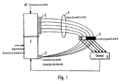
- a sensor 6 can be used, which is introduced into the lighting system for the calibration measurement.
- the correction factor may be dependent on a color measurement.
- the color measurement can be done by means of an RGB color measurement, for example a CCD sensor.
- the sensor 6 would be an RGB color sensor.
- the determination of the correction factor can be repeated at regular intervals.
- the memory can be read out by the driver module via a digital interface.
- the memory can be located on the LED module and can be read by the user when the module is replaced.
- the memory may be located on the LED module and prior to replacement of the module by the driver module due to user signaling be read out.
- the memory may be placed in a calibrator.
- the signaling for reading the memory on the LED module can be done by the user by a switching sequence on the supply voltage, a digital control command or by other signaling.
- the information read out can be stored in the memory of the new LED module.
- the driver module can forward the information stored in memory via a digital interface to other driver modules.
- one or more LED modules can be switched off.
- only one LED module can be switched on at a time.
- the color measurement can be performed with a color sensor (eg CCD sensor).
- a color sensor eg CCD sensor
- the color sensor may be placed so that it can receive a portion of the light emitted by the LED modules.
- the color sensor may be placed so that it is shielded from ambient light and can receive only light emitted by the LED modules. This foreclosure can be done by a cover that is specially designed for the calibration measurement. On this cover 11, the sensor 6 may be located. The sensor 6 can also be on the reflector 10 of the LED Luminaire be placed. The sensor 6 may be placed to directly or indirectly receive the light of the LED 5 of the LED module.
- the color location and the intensity of the LED 5 can be stored.
- the individual LED modules can be switched on and calibrated one after the other.
- the calibration can be used to determine the colors of the connected LED modules.
- the individual colors or color locations as well as the intensities of the respectively driven LEDs 5 are determined. From the combination of the individual calibration measurements, which are carried out in succession, the assignment of the colors and the mixture of the individual LEDs 5 required for the output of a desired color by the LED illumination can be determined.
- the driver module may include a switching regulator, such as an AC-DC converter, a DC-DC converter, a current sink, or a power source.
- the driver module may include a PFC (Active Power Factor Correction Circuit), or a PFC (Active Power Factor Correction Circuit) may precede the driver module.
- the driver module can have a potential separation.
- the operation of the LEDs may be such that the LED module is driven by at least one LED from a driver module, and a memory for storing information about the LED module is present, wherein Information can be stored or modified in memory. The information in the memory can be changed based on a calibration measurement.
- the driver module can be formed by a switching regulator or by a current sink or a current source. If a switching regulator is used as the driver module, then it can internally operate at a higher frequency than the frequency with which the LED or the LED module is controlled.
- the internal frequency with which the switch of the switching regulator is controlled can be in the range of 10 kHz to several MHz, while this internal frequency is superimposed on a low frequency corresponding to the frequency of the at least one PWM packet.
- the information in the memory can be changed by a correction factor.
- a method for operating at least two light sources wherein electric energy is provided to at least two illuminant arrangements, each consisting of one or more bulbs, by a common electrical supply unit, wherein a first illuminant arrangement and at least one second illuminant arrangement contains electrical energy Form of PWM packets is supplied, wherein the timing of the PWM packets is tuned between the different illuminant arrangements.
- Examples of the control of three lamp assemblies are in the 3 and 4 represented, wherein the lamp assemblies electrical energy can be supplied in the form of PWM packets.
- the at least two illuminant arrangements can be controlled such that the time center of a PWM packet of the first illuminant arrangement coincides with the temporal midpoint of a PWM packet of at least one second illuminant arrangement or follows one another closely in time.
- Fig. 4 is an example of a control with an offset of the time centers of the individual PWM signals shown.
- the timing of the PWM packets can be coordinated over the entire dimming range of the lamps.
- the at least two illuminant arrangements can be controlled such that, alternatively or additionally, the time centers of the PWM packets of the illuminant arrangements are shifted in time with respect to one another with an offset value, so that the flanks of the PWM packets to the illuminant arrangements do not occur at the same time.
- the switch-on edge of at least one of a plurality of parallel PWM signals may be shifted in time to at least one further PWM signal, so that the problem of simultaneous PWM control no longer exists.
- This offset (offset value) can be internally or externally variable or fixed.
- the offset could correspond to the entire turn-off phase of a PWM signal, ie, with the pulse duty ratio unchanged, the corresponding LED within a PWM period becomes first switched off and then turned on.
- a PWM signal can therefore be inverted, ie at the start of each cycle, triggered by an interrupt signal, for example, the switch-off phase and only then the switch-on phase of the LED can be controlled.
- the offset could also be chosen such that the turn-on edges for the PWM signals are generated uniformly distributed over the PWM period.
- a third alternative is to randomly select offset. In Fig. 3 an example of a drive with an offset of the individual PWM signals is shown.
- the offset may already be present during the generation of the PWM signals, or else be inserted deliberately in the case of simultaneously generated PWM signals on the path between the PWM generation and the LEDs.
- the PWM signals can be generated starting from one or even from several clocks.
- the offset value can be selected depending on the dimming level of the lamps.
- the frequency of at least one PWM signal may also change at least temporarily, so that a combined PWM / FM (frequency modulation) is present. It would be conceivable, for example, to set the frequency as a function of the duty cycle of the PWM signal.
- the frequency of at least one PWM signal at least temporarily from the distinguish at least one other PWM signal.
- one or more clocks may be present.
- one frequency may be a multiple of another frequency.
- At least one frequency can be shifted after generation of uniform PWM switching frequencies, for example by a capacitor.
- the hardware then adopts the new value at the next zero crossing of the period.
- the center PWM method (triangle as in Fig. 4 shown) comes at different PWM position, none of the flanks directly at the same time to change up to four channels.
- the only exception here is with the same dimming position all flanks on each other, but could be integrated as an improvement after the calculation so that is played with the PWM resolution, ie that deliberately shifts the channels by 1 bit PWM to achieve a blurring (see example of Fig. 3 ).
- the luminous means of the first and / or at least the second luminous means arrangement can be inorganic or organic light-emitting diodes.
- the lighting means of the first and / or at least the second lighting arrangement can emit a different light spectrum.
- an operating device can be made possible in the above-mentioned method can be performed.
- an illumination system can be made possible which has at least two light sources in which a method or operating device mentioned above is used.
- Fig. 2 schematically a circuit for the controlled operation of light-emitting diodes (LED) is shown, which represents an example of a driver module.
- LED light-emitting diodes
- two light-emitting diodes are connected in series, however, it is just an advantage of the present invention that the operating circuit adapts very flexibly to the type and number of light-emitting diodes (LED) also connected in series.
- the operating circuit is supplied with an input DC voltage Vin, which of course can also be a rectified AC voltage.
- a series circuit between a semiconductor power switch S1 (for example, a MOSFET) and a freewheeling diode D1 energizes in the switched-on state of the switch S1 an inductance L1 by means of the current flowing through the switch.
- a semiconductor power switch S1 for example, a MOSFET
- a freewheeling diode D1 energizes in the switched-on state of the switch S1 an inductance L1 by means of the current flowing through the switch.
- the energy stored in the coil L1 discharges in the form of a current i through a capacitor C1 and the light-emitting diode path LED.
- control and / or regulating circuit SR which specifies the timing of the switch S1, for example in the form of harnessfreugenten modulated signals as a manipulated variable of the control of the LED power.
- the control and / or regulating circuit SR can, for example, apply a hysteretic current regulation.
- the control and / or regulating circuit SR detects the current through the switch S1 (in the switched-on state of the switch S1).
- control and / or regulating unit SR can detect the potential on the lower-potential side of the LED path.
- Another voltage divider R3, R4 allows the detection of the supply voltage.
- the driver module is formed in this example by a buck converter, but can also be formed for example by a boost converter, buck-boost converter or other switching regulator or by a current sink or a power source.
- the switch S1 is driven internally by the control and / or regulating circuit SR at a higher frequency than the frequency, as with which the LED or the LED module are controlled.
- the internal frequency with which the switch S1 of the switching regulator is controlled may be in the range of 10 kHz to several MHz, while this internal frequency is superimposed on a low frequency which corresponds to the frequency of the at least one PWM packet.
- the LED module may be driven with a low frequency PWM packet, which PWM packet may ripple due to the high frequency operation of the switch S1 of the driver module during turn-on time.
- the ripple that may result due to the high frequency operation of the switch S1 of the driver module may be reduced by the capacitor C1.
- the low frequency of the at least one PWM packet that is superimposed may be dictated by an external controller such as a microcontroller or other central control unit.
- an external controller such as a microcontroller or other central control unit.
- the three colors of the RGB LED module can each be driven by one driver module, the three driver modules being controlled via three PWM channels.
Landscapes
- Circuit Arrangement For Electric Light Sources In General (AREA)
Claims (12)
- Dispositif pour le fonctionnement d'au moins deux agencements de moyens d'éclairage, consistant respectivement en un ou plusieurs moyens d'éclairage, de préférence LEDs, le dispositif mettant de l'énergie électrique à disposition desdits au moins deux agencements de moyens d'éclairage,
et dans lequel de l'énergie électrique est fournie sous forme de paquets MLI à un premier agencement de moyens d'éclairage et au moins un deuxième agencement de moyens d'éclairage,
caractérisé en ce que
le flanc montant d'au moins un paquet MLI d'un premier agencement de moyens d'éclairage diffère au moins temporairement du flanc montant d'au moins un autre paquet MLI d'un deuxième agencement de moyens d'éclairage,
dans lequel lesdits au moins deux agencements de moyens d'éclairage sont commandés de telle sorte que le point central dans le temps d'un paquet MLI du premier agencement de moyens d'éclairage correspond au point central dans le temps d'un paquet MLI d'au moins un deuxième agencement de moyens d'éclairage ou lui succède de manière proche dans le temps. - Dispositif selon la revendication 1, caractérisé en ce que la coordination de la séquence temporelle des paquets MLI a lieu sur toute la plage de gradation des moyens d'éclairage.
- Dispositif selon l'une des revendications précédentes, caractérisé en ce que les au moins deux agencements de moyens d'éclairage sont commandés de telle sorte qu'en outre les points centraux dans le temps des paquets MLI des agencements de moyens d'éclairage sont décalés temporellement les uns par rapport aux autres d'une valeur de décalage, pour que les flancs des paquets MLI n'arrivent pas simultanément aux agencements de moyens d'éclairage,
dans lequel la valeur de décalage est choisie en fonction du niveau de gradation des moyens d'éclairage. - Dispositif selon l'une des revendications précédentes, caractérisé en ce que les moyens d'éclairage du premier et/ou d'au moins le deuxième agencement de moyens d'éclairage sont des diodes électroluminescentes anorganiques ou organiques.
- Dispositif selon l'une des revendications précédentes, caractérisé en ce que les moyens d'éclairage du premier et/ou d'au moins le deuxième agencement de moyens d'éclairage émettent un spectre lumineux différent.
- Dispositif selon l'une des revendications précédentes,
dans lequel l'écart temporel des flancs montants est variable de manière interne ou externe ou est prédéterminé de manière fixe. - Dispositif selon l'une des revendications précédentes,
dans lequel l'écart temporel est déjà présent au moment de la génération des signaux MLI, et/ou est inséré de manière ciblée sur le trajet entre la génération MLI et les LEDs. - Dispositif selon l'une des revendications précédentes,
caractérisé en ce que
la fréquence d'au moins un paquet MLI diffère au moins temporairement de la fréquence d'au moins un autre paquet MLI d'un deuxième agencement de moyens d'éclairage,
dans lequel la fréquence d'un paquet MLI est un multiple d'une autre fréquence. - Dispositif selon la revendication 8,
dans lequel au moins une fréquence est décalée après la génération de fréquences de commutation MLI uniformes par exemple par un condensateur. - Appareil de commande, présentant un dispositif selon l'une des revendications précédentes.
- Système d'éclairage présentant au moins deux moyens d'éclairage et deux dispositifs selon l'une des revendications 1 à 9, les deux dispositifs étant reliés entre eux de manière fonctionnelle.
- Procédé pour réduire la charge d'une alimentation en tension et/ou pour améliorer la compatibilité électromagnétique lors de la commande de LEDs avec des signaux MLI,
dans lequel le flanc montant d'au moins un signal MLI diffèrent temporellement de celui d'au moins un autre signal MLI au moins temporairement et, ainsi, n'est pas simultané avec celui-ci,
dans lequel les au moins deux agencements de moyens d'éclairage sont commandés de telle sorte que le point central dans le temps d'un paquet MLI du premier agencement de moyens d'éclairage correspond au point central dans le temps d'un paquet MLI d'au moins un deuxième agencement de moyens d'éclairage ou lui succède de manière proche dans le temps.
Applications Claiming Priority (3)
| Application Number | Priority Date | Filing Date | Title |
|---|---|---|---|
| AT7462008 | 2008-12-23 | ||
| DE102009005819A DE102009005819A1 (de) | 2008-12-23 | 2009-01-22 | Verfahren und Vorrichtung zum Betreiben von LEDs |
| PCT/EP2009/067631 WO2010081613A1 (fr) | 2008-12-23 | 2009-12-21 | Procédé et dispositif permettant de faire fonctionner des groupes de led au moyen de la pwm |
Publications (2)
| Publication Number | Publication Date |
|---|---|
| EP2368407A1 EP2368407A1 (fr) | 2011-09-28 |
| EP2368407B1 true EP2368407B1 (fr) | 2014-03-19 |
Family
ID=42220959
Family Applications (1)
| Application Number | Title | Priority Date | Filing Date |
|---|---|---|---|
| EP09799347.1A Active EP2368407B1 (fr) | 2008-12-23 | 2009-12-21 | Procédé et dispositif permettant de faire fonctionner des groupes de led au moyen de la pwm |
Country Status (3)
| Country | Link |
|---|---|
| EP (1) | EP2368407B1 (fr) |
| DE (2) | DE102009005819A1 (fr) |
| WO (1) | WO2010081613A1 (fr) |
Family Cites Families (6)
| Publication number | Priority date | Publication date | Assignee | Title |
|---|---|---|---|---|
| AU6034394A (en) | 1993-02-11 | 1994-08-29 | Louis A. Phares | Controlled lighting system |
| US6016038A (en) | 1997-08-26 | 2000-01-18 | Color Kinetics, Inc. | Multicolored LED lighting method and apparatus |
| TWI277225B (en) * | 2005-08-03 | 2007-03-21 | Beyond Innovation Tech Co Ltd | Apparatus of light source and adjustable control circuit for LEDs |
| DE102005049579A1 (de) * | 2005-10-17 | 2007-04-19 | Patent-Treuhand-Gesellschaft für elektrische Glühlampen mbH | Lichtquelle, die mischfarbiges Licht aussendet, und Verfahren zur Steuerung des Farbortes einer solchen Lichtquelle |
| US20080048582A1 (en) * | 2006-08-28 | 2008-02-28 | Robinson Shane P | Pwm method and apparatus, and light source driven thereby |
| US7948468B2 (en) * | 2007-02-23 | 2011-05-24 | The Regents Of The University Of Colorado | Systems and methods for driving multiple solid-state light sources |
-
2009
- 2009-01-22 DE DE102009005819A patent/DE102009005819A1/de not_active Withdrawn
- 2009-12-21 EP EP09799347.1A patent/EP2368407B1/fr active Active
- 2009-12-21 DE DE112009003815T patent/DE112009003815A5/de not_active Withdrawn
- 2009-12-21 WO PCT/EP2009/067631 patent/WO2010081613A1/fr not_active Ceased
Also Published As
| Publication number | Publication date |
|---|---|
| WO2010081613A1 (fr) | 2010-07-22 |
| EP2368407A1 (fr) | 2011-09-28 |
| DE102009005819A1 (de) | 2010-07-01 |
| DE112009003815A5 (de) | 2012-08-02 |
Similar Documents
| Publication | Publication Date | Title |
|---|---|---|
| EP2474200B1 (fr) | Fonctionnement de led à modulation d'impulsions | |
| DE10013207B4 (de) | Ansteuerung von Leuchtdioden (LED's) | |
| EP2019569B1 (fr) | Procédé d'atténuation de la luminosité rayonnée par des lampes à DEL, en particulier dans la cabine d'un avion commercial | |
| EP2522199B1 (fr) | Procédé combiné pour faire fonctionner un élément luminescent électrique et circuit d'exploitation | |
| EP2792217B1 (fr) | Dispositifs d'éclairage comprenant des convertisseurs élévateurs pour contrôler la chromaticité et/ou la luminosité et procédés associés | |
| US8796957B2 (en) | Multi-string LED driving method and system | |
| DE102016112550A1 (de) | Beleuchtungsbaugruppe, fahrzeugbeleuchtungseinrichtung und fahrzeug | |
| DE102009000042A1 (de) | Mehrfach-LED-Treiber | |
| DE102016125547A1 (de) | Stromversorgungseinrichtung und leuchte | |
| DE202013004095U1 (de) | LED-Beleuchtungssystem | |
| EP2548412B1 (fr) | Système d'éclairage à del | |
| EP3064038B1 (fr) | Circuit de commande d'élément luminescent comportant un convertisseur cadencé pour le réglage numérique d'une température de couleur et/ou d'un niveau de variation d'intensité lumineuse | |
| EP2772120B1 (fr) | Atténuation de moyens d'éclairage par modulation d'impulsions en largeur pwm | |
| DE102012018760A1 (de) | Vorrichtung zum Betreiben von LEDs | |
| EP2280585A2 (fr) | Procédé de réglage de la commande de plusieurs lampes | |
| EP2368407B1 (fr) | Procédé et dispositif permettant de faire fonctionner des groupes de led au moyen de la pwm | |
| EP2425679B1 (fr) | Circuit d'excitation pour une led | |
| EP2777364B1 (fr) | Procédé de fonctionnement d'au moins une del par vibrations | |
| DE202017002443U1 (de) | Schaltungsanordnung zum Betreiben eines Leuchtmittels | |
| DE102014208305A1 (de) | Kapazitätsfreier LED-Treiber | |
| DE102017223405A1 (de) | Betriebsschaltung für ein LED-Leuchtmittel | |
| DE102018115672A1 (de) | Betriebsgerät für mehrere Leuchtmittel, Leuchtmittel und Beleuchtungssystem | |
| EP4099803A1 (fr) | Module de del blanche réglable | |
| AT518887B1 (de) | Vorrichtung zum betreiben von leds | |
| DE202016107324U1 (de) | Schaltungsanordnung zum Betreiben von Leuchtmitteln |
Legal Events
| Date | Code | Title | Description |
|---|---|---|---|
| PUAI | Public reference made under article 153(3) epc to a published international application that has entered the european phase |
Free format text: ORIGINAL CODE: 0009012 |
|
| 17P | Request for examination filed |
Effective date: 20110609 |
|
| AK | Designated contracting states |
Kind code of ref document: A1 Designated state(s): AT BE BG CH CY CZ DE DK EE ES FI FR GB GR HR HU IE IS IT LI LT LU LV MC MK MT NL NO PL PT RO SE SI SK SM TR |
|
| DAX | Request for extension of the european patent (deleted) | ||
| 17Q | First examination report despatched |
Effective date: 20120417 |
|
| GRAP | Despatch of communication of intention to grant a patent |
Free format text: ORIGINAL CODE: EPIDOSNIGR1 |
|
| INTG | Intention to grant announced |
Effective date: 20131018 |
|
| GRAS | Grant fee paid |
Free format text: ORIGINAL CODE: EPIDOSNIGR3 |
|
| GRAA | (expected) grant |
Free format text: ORIGINAL CODE: 0009210 |
|
| AK | Designated contracting states |
Kind code of ref document: B1 Designated state(s): AT BE BG CH CY CZ DE DK EE ES FI FR GB GR HR HU IE IS IT LI LT LU LV MC MK MT NL NO PL PT RO SE SI SK SM TR |
|
| REG | Reference to a national code |
Ref country code: GB Ref legal event code: FG4D Free format text: NOT ENGLISH |
|
| REG | Reference to a national code |
Ref country code: CH Ref legal event code: EP |
|
| REG | Reference to a national code |
Ref country code: IE Ref legal event code: FG4D Free format text: LANGUAGE OF EP DOCUMENT: GERMAN |
|
| REG | Reference to a national code |
Ref country code: AT Ref legal event code: REF Ref document number: 658398 Country of ref document: AT Kind code of ref document: T Effective date: 20140415 |
|
| REG | Reference to a national code |
Ref country code: DE Ref legal event code: R096 Ref document number: 502009009040 Country of ref document: DE Effective date: 20140430 |
|
| PG25 | Lapsed in a contracting state [announced via postgrant information from national office to epo] |
Ref country code: LT Free format text: LAPSE BECAUSE OF FAILURE TO SUBMIT A TRANSLATION OF THE DESCRIPTION OR TO PAY THE FEE WITHIN THE PRESCRIBED TIME-LIMIT Effective date: 20140319 Ref country code: NO Free format text: LAPSE BECAUSE OF FAILURE TO SUBMIT A TRANSLATION OF THE DESCRIPTION OR TO PAY THE FEE WITHIN THE PRESCRIBED TIME-LIMIT Effective date: 20140619 |
|
| REG | Reference to a national code |
Ref country code: NL Ref legal event code: VDEP Effective date: 20140319 |
|
| REG | Reference to a national code |
Ref country code: LT Ref legal event code: MG4D |
|
| PG25 | Lapsed in a contracting state [announced via postgrant information from national office to epo] |
Ref country code: CY Free format text: LAPSE BECAUSE OF FAILURE TO SUBMIT A TRANSLATION OF THE DESCRIPTION OR TO PAY THE FEE WITHIN THE PRESCRIBED TIME-LIMIT Effective date: 20140319 Ref country code: FI Free format text: LAPSE BECAUSE OF FAILURE TO SUBMIT A TRANSLATION OF THE DESCRIPTION OR TO PAY THE FEE WITHIN THE PRESCRIBED TIME-LIMIT Effective date: 20140319 Ref country code: SE Free format text: LAPSE BECAUSE OF FAILURE TO SUBMIT A TRANSLATION OF THE DESCRIPTION OR TO PAY THE FEE WITHIN THE PRESCRIBED TIME-LIMIT Effective date: 20140319 |
|
| PG25 | Lapsed in a contracting state [announced via postgrant information from national office to epo] |
Ref country code: HR Free format text: LAPSE BECAUSE OF FAILURE TO SUBMIT A TRANSLATION OF THE DESCRIPTION OR TO PAY THE FEE WITHIN THE PRESCRIBED TIME-LIMIT Effective date: 20140319 Ref country code: LV Free format text: LAPSE BECAUSE OF FAILURE TO SUBMIT A TRANSLATION OF THE DESCRIPTION OR TO PAY THE FEE WITHIN THE PRESCRIBED TIME-LIMIT Effective date: 20140319 |
|
| PG25 | Lapsed in a contracting state [announced via postgrant information from national office to epo] |
Ref country code: NL Free format text: LAPSE BECAUSE OF FAILURE TO SUBMIT A TRANSLATION OF THE DESCRIPTION OR TO PAY THE FEE WITHIN THE PRESCRIBED TIME-LIMIT Effective date: 20140319 Ref country code: CZ Free format text: LAPSE BECAUSE OF FAILURE TO SUBMIT A TRANSLATION OF THE DESCRIPTION OR TO PAY THE FEE WITHIN THE PRESCRIBED TIME-LIMIT Effective date: 20140319 Ref country code: BG Free format text: LAPSE BECAUSE OF FAILURE TO SUBMIT A TRANSLATION OF THE DESCRIPTION OR TO PAY THE FEE WITHIN THE PRESCRIBED TIME-LIMIT Effective date: 20140619 Ref country code: IS Free format text: LAPSE BECAUSE OF FAILURE TO SUBMIT A TRANSLATION OF THE DESCRIPTION OR TO PAY THE FEE WITHIN THE PRESCRIBED TIME-LIMIT Effective date: 20140719 Ref country code: RO Free format text: LAPSE BECAUSE OF FAILURE TO SUBMIT A TRANSLATION OF THE DESCRIPTION OR TO PAY THE FEE WITHIN THE PRESCRIBED TIME-LIMIT Effective date: 20140319 Ref country code: EE Free format text: LAPSE BECAUSE OF FAILURE TO SUBMIT A TRANSLATION OF THE DESCRIPTION OR TO PAY THE FEE WITHIN THE PRESCRIBED TIME-LIMIT Effective date: 20140319 |
|
| PG25 | Lapsed in a contracting state [announced via postgrant information from national office to epo] |
Ref country code: SK Free format text: LAPSE BECAUSE OF FAILURE TO SUBMIT A TRANSLATION OF THE DESCRIPTION OR TO PAY THE FEE WITHIN THE PRESCRIBED TIME-LIMIT Effective date: 20140319 Ref country code: PL Free format text: LAPSE BECAUSE OF FAILURE TO SUBMIT A TRANSLATION OF THE DESCRIPTION OR TO PAY THE FEE WITHIN THE PRESCRIBED TIME-LIMIT Effective date: 20140319 Ref country code: ES Free format text: LAPSE BECAUSE OF FAILURE TO SUBMIT A TRANSLATION OF THE DESCRIPTION OR TO PAY THE FEE WITHIN THE PRESCRIBED TIME-LIMIT Effective date: 20140319 |
|
| REG | Reference to a national code |
Ref country code: DE Ref legal event code: R097 Ref document number: 502009009040 Country of ref document: DE |
|
| PG25 | Lapsed in a contracting state [announced via postgrant information from national office to epo] |
Ref country code: PT Free format text: LAPSE BECAUSE OF FAILURE TO SUBMIT A TRANSLATION OF THE DESCRIPTION OR TO PAY THE FEE WITHIN THE PRESCRIBED TIME-LIMIT Effective date: 20140721 |
|
| PLBE | No opposition filed within time limit |
Free format text: ORIGINAL CODE: 0009261 |
|
| STAA | Information on the status of an ep patent application or granted ep patent |
Free format text: STATUS: NO OPPOSITION FILED WITHIN TIME LIMIT |
|
| PG25 | Lapsed in a contracting state [announced via postgrant information from national office to epo] |
Ref country code: DK Free format text: LAPSE BECAUSE OF FAILURE TO SUBMIT A TRANSLATION OF THE DESCRIPTION OR TO PAY THE FEE WITHIN THE PRESCRIBED TIME-LIMIT Effective date: 20140319 |
|
| 26N | No opposition filed |
Effective date: 20141222 |
|
| PG25 | Lapsed in a contracting state [announced via postgrant information from national office to epo] |
Ref country code: IT Free format text: LAPSE BECAUSE OF FAILURE TO SUBMIT A TRANSLATION OF THE DESCRIPTION OR TO PAY THE FEE WITHIN THE PRESCRIBED TIME-LIMIT Effective date: 20140319 |
|
| REG | Reference to a national code |
Ref country code: DE Ref legal event code: R097 Ref document number: 502009009040 Country of ref document: DE Effective date: 20141222 |
|
| PG25 | Lapsed in a contracting state [announced via postgrant information from national office to epo] |
Ref country code: BE Free format text: LAPSE BECAUSE OF NON-PAYMENT OF DUE FEES Effective date: 20141231 |
|
| PG25 | Lapsed in a contracting state [announced via postgrant information from national office to epo] |
Ref country code: LU Free format text: LAPSE BECAUSE OF FAILURE TO SUBMIT A TRANSLATION OF THE DESCRIPTION OR TO PAY THE FEE WITHIN THE PRESCRIBED TIME-LIMIT Effective date: 20141221 Ref country code: SI Free format text: LAPSE BECAUSE OF FAILURE TO SUBMIT A TRANSLATION OF THE DESCRIPTION OR TO PAY THE FEE WITHIN THE PRESCRIBED TIME-LIMIT Effective date: 20140319 |
|
| REG | Reference to a national code |
Ref country code: CH Ref legal event code: PL |
|
| REG | Reference to a national code |
Ref country code: IE Ref legal event code: MM4A |
|
| PG25 | Lapsed in a contracting state [announced via postgrant information from national office to epo] |
Ref country code: CH Free format text: LAPSE BECAUSE OF NON-PAYMENT OF DUE FEES Effective date: 20141231 Ref country code: LI Free format text: LAPSE BECAUSE OF NON-PAYMENT OF DUE FEES Effective date: 20141231 Ref country code: IE Free format text: LAPSE BECAUSE OF NON-PAYMENT OF DUE FEES Effective date: 20141221 |
|
| REG | Reference to a national code |
Ref country code: FR Ref legal event code: PLFP Year of fee payment: 7 |
|
| PG25 | Lapsed in a contracting state [announced via postgrant information from national office to epo] |
Ref country code: SM Free format text: LAPSE BECAUSE OF FAILURE TO SUBMIT A TRANSLATION OF THE DESCRIPTION OR TO PAY THE FEE WITHIN THE PRESCRIBED TIME-LIMIT Effective date: 20140319 |
|
| PG25 | Lapsed in a contracting state [announced via postgrant information from national office to epo] |
Ref country code: MC Free format text: LAPSE BECAUSE OF FAILURE TO SUBMIT A TRANSLATION OF THE DESCRIPTION OR TO PAY THE FEE WITHIN THE PRESCRIBED TIME-LIMIT Effective date: 20140319 |
|
| PG25 | Lapsed in a contracting state [announced via postgrant information from national office to epo] |
Ref country code: GR Free format text: LAPSE BECAUSE OF FAILURE TO SUBMIT A TRANSLATION OF THE DESCRIPTION OR TO PAY THE FEE WITHIN THE PRESCRIBED TIME-LIMIT Effective date: 20140620 |
|
| PG25 | Lapsed in a contracting state [announced via postgrant information from national office to epo] |
Ref country code: MT Free format text: LAPSE BECAUSE OF FAILURE TO SUBMIT A TRANSLATION OF THE DESCRIPTION OR TO PAY THE FEE WITHIN THE PRESCRIBED TIME-LIMIT Effective date: 20140319 Ref country code: TR Free format text: LAPSE BECAUSE OF FAILURE TO SUBMIT A TRANSLATION OF THE DESCRIPTION OR TO PAY THE FEE WITHIN THE PRESCRIBED TIME-LIMIT Effective date: 20140319 Ref country code: HU Free format text: LAPSE BECAUSE OF FAILURE TO SUBMIT A TRANSLATION OF THE DESCRIPTION OR TO PAY THE FEE WITHIN THE PRESCRIBED TIME-LIMIT; INVALID AB INITIO Effective date: 20091221 |
|
| REG | Reference to a national code |
Ref country code: FR Ref legal event code: PLFP Year of fee payment: 8 |
|
| REG | Reference to a national code |
Ref country code: FR Ref legal event code: PLFP Year of fee payment: 9 |
|
| PGFP | Annual fee paid to national office [announced via postgrant information from national office to epo] |
Ref country code: AT Payment date: 20171228 Year of fee payment: 9 |
|
| PG25 | Lapsed in a contracting state [announced via postgrant information from national office to epo] |
Ref country code: MK Free format text: LAPSE BECAUSE OF FAILURE TO SUBMIT A TRANSLATION OF THE DESCRIPTION OR TO PAY THE FEE WITHIN THE PRESCRIBED TIME-LIMIT Effective date: 20140319 |
|
| REG | Reference to a national code |
Ref country code: DE Ref legal event code: R084 Ref document number: 502009009040 Country of ref document: DE |
|
| PGFP | Annual fee paid to national office [announced via postgrant information from national office to epo] |
Ref country code: FR Payment date: 20181231 Year of fee payment: 10 |
|
| REG | Reference to a national code |
Ref country code: AT Ref legal event code: MM01 Ref document number: 658398 Country of ref document: AT Kind code of ref document: T Effective date: 20181221 |
|
| REG | Reference to a national code |
Ref country code: DE Ref legal event code: R079 Ref document number: 502009009040 Country of ref document: DE Free format text: PREVIOUS MAIN CLASS: H05B0033080000 Ipc: H05B0045000000 |
|
| PG25 | Lapsed in a contracting state [announced via postgrant information from national office to epo] |
Ref country code: AT Free format text: LAPSE BECAUSE OF NON-PAYMENT OF DUE FEES Effective date: 20181221 |
|
| PGFP | Annual fee paid to national office [announced via postgrant information from national office to epo] |
Ref country code: GB Payment date: 20191226 Year of fee payment: 11 |
|
| PG25 | Lapsed in a contracting state [announced via postgrant information from national office to epo] |
Ref country code: FR Free format text: LAPSE BECAUSE OF NON-PAYMENT OF DUE FEES Effective date: 20191231 |
|
| GBPC | Gb: european patent ceased through non-payment of renewal fee |
Effective date: 20201221 |
|
| PG25 | Lapsed in a contracting state [announced via postgrant information from national office to epo] |
Ref country code: GB Free format text: LAPSE BECAUSE OF NON-PAYMENT OF DUE FEES Effective date: 20201221 |
|
| P01 | Opt-out of the competence of the unified patent court (upc) registered |
Effective date: 20230530 |
|
| PGFP | Annual fee paid to national office [announced via postgrant information from national office to epo] |
Ref country code: DE Payment date: 20241227 Year of fee payment: 16 |