EP2400560A1 - Solar battery module - Google Patents
Solar battery module Download PDFInfo
- Publication number
- EP2400560A1 EP2400560A1 EP10743760A EP10743760A EP2400560A1 EP 2400560 A1 EP2400560 A1 EP 2400560A1 EP 10743760 A EP10743760 A EP 10743760A EP 10743760 A EP10743760 A EP 10743760A EP 2400560 A1 EP2400560 A1 EP 2400560A1
- Authority
- EP
- European Patent Office
- Prior art keywords
- solar cell
- light
- solar cells
- cell module
- receiving surface
- Prior art date
- Legal status (The legal status is an assumption and is not a legal conclusion. Google has not performed a legal analysis and makes no representation as to the accuracy of the status listed.)
- Granted
Links
Images

Classifications
-
- H—ELECTRICITY
- H10—SEMICONDUCTOR DEVICES; ELECTRIC SOLID-STATE DEVICES NOT OTHERWISE PROVIDED FOR
- H10F—INORGANIC SEMICONDUCTOR DEVICES SENSITIVE TO INFRARED RADIATION, LIGHT, ELECTROMAGNETIC RADIATION OF SHORTER WAVELENGTH OR CORPUSCULAR RADIATION
- H10F19/00—Integrated devices, or assemblies of multiple devices, comprising at least one photovoltaic cell covered by group H10F10/00, e.g. photovoltaic modules
- H10F19/90—Structures for connecting between photovoltaic cells, e.g. interconnections or insulating spacers
- H10F19/902—Structures for connecting between photovoltaic cells, e.g. interconnections or insulating spacers for series or parallel connection of photovoltaic cells
-
- H—ELECTRICITY
- H10—SEMICONDUCTOR DEVICES; ELECTRIC SOLID-STATE DEVICES NOT OTHERWISE PROVIDED FOR
- H10F—INORGANIC SEMICONDUCTOR DEVICES SENSITIVE TO INFRARED RADIATION, LIGHT, ELECTROMAGNETIC RADIATION OF SHORTER WAVELENGTH OR CORPUSCULAR RADIATION
- H10F77/00—Constructional details of devices covered by this subclass
-
- Y—GENERAL TAGGING OF NEW TECHNOLOGICAL DEVELOPMENTS; GENERAL TAGGING OF CROSS-SECTIONAL TECHNOLOGIES SPANNING OVER SEVERAL SECTIONS OF THE IPC; TECHNICAL SUBJECTS COVERED BY FORMER USPC CROSS-REFERENCE ART COLLECTIONS [XRACs] AND DIGESTS
- Y02—TECHNOLOGIES OR APPLICATIONS FOR MITIGATION OR ADAPTATION AGAINST CLIMATE CHANGE
- Y02E—REDUCTION OF GREENHOUSE GAS [GHG] EMISSIONS, RELATED TO ENERGY GENERATION, TRANSMISSION OR DISTRIBUTION
- Y02E10/00—Energy generation through renewable energy sources
- Y02E10/50—Photovoltaic [PV] energy
Definitions
- This invention relates to a solar cell module comprising solar cells in the form of semiconductor devices.
- a solar cell module fabricated from crystalline solar cells is generally manufactured by providing solar cells based solely on substrates of one conductivity type and connecting the cells in series for the purpose of increasing the voltage.
- cells each have an electrode of first polarity on a light-receiving surface side and an electrode of second polarity (opposite to the first polarity) on a non-light-receiving surface side are used, then the electrode of first polarity on the light-receiving surface side must be connected to the electrode of second polarity on the non-light-receiving surface side by a conductor containing solder and other components (referred to as "tab wire") in order to achieve series connection.
- Those electrodes which are connected by the tab wire are electrodes of a relatively large width (about 1 to 3 mm) and generally known as bus-bar electrodes.
- Patent Document 1 proposes a solar cell module in which a tab wire is provided with a pre-bent portion, and the tab wire is connected such that the bent portion is disposed between adjacent cells, thereby reducing the bending stress of the tab wire and preventing cell edge failure.
- An object of the invention which has been made under the aforementioned circumstances, is to provide a solar cell module which is improved in module conversion efficiency by increasing the packing density of solar cells relative to the area of the solar cell module.
- a solar cell module is constructed in which the first solar cell having an electrode of first polarity and the second solar cell having an electrode of second polarity opposite to the first polarity are juxtaposed in a common plane.
- This arrangement ensures that the first and second solar cells are connected in series by connecting the electrodes on the light-receiving surface to each other and the electrodes on the non-light-receiving surface to each other with tab wires, and the cells are closely arranged at a spacing of 3.0 mm or less, whereby the packing density of solar cells relative to the area of the solar cell module may be increased, leading to improved module conversion efficiency.
- the arrangement facilitates attachment of the tab wires and eliminates the stress due to the tab wires, preventing cell edge failure and increasing the yield of manufacture, which ensures fabrication of a highly reliable solar cell module.
- the invention is predicated on these findings.
- electrodes on the light-receiving and non-light-receiving surfaces thin electrodes of about 50 to 200 ⁇ m wide which are formed on the solar cell front surface across bus-bar electrodes for collecting outputs are referred to as "finger electrodes", and relatively thick electrodes of about 1 to 3 mm wide for taking out the output collected by the finger electrodes are referred to as "bus-bar electrodes”.
- the invention provides a solar cell module as defined below.
- the solar cell arrangement and interconnecting method according to the invention permit the packing density of solar cells relative to the area of the solar cell module to be increased, whereby the module conversion efficiency is improved. Additionally, since the stress applied from tab wires to the edge of solar cells can be reduced as compared with the prior art method, a highly reliable solar cell module can be fabricated in improved manufacture yields.
- the invention is directed to a solar cell module in which a first solar cell(s) comprising a first conductivity type substrate having a light-receiving surface and a non-light-receiving surface and electrodes of opposite polarity formed on the light-receiving and non-light-receiving surfaces, respectively, and a second solar cell(s) comprising a second conductivity type substrate having a light-receiving surface and a non-light-receiving surface and electrodes of opposite polarity formed on the light-receiving and non-light-receiving surfaces, respectively, are alternately arranged.
- This solar cell module is constructed as shown in FIG.
- the conductivity type of the substrate of the first solar cell is opposite to the conductivity type of the substrate of the second solar cell.
- the former is n-type
- the latter is p-type.
- the polarity of the electrode on the light-receiving surface of the substrate of the first solar cell is identical with the polarity of the electrode on the non-light-receiving surface of the substrate of the second solar cell, while the electrode on the non-light-receiving surface of the substrate of the first solar cell and the electrode on the light-receiving surface of the substrate of the second solar cell are of the same polarity.
- the electrode on the non-light-receiving surface of the substrate of the first solar cell and the electrode on the light-receiving surface of the substrate of the second solar cell are of the same polarity.
- the second solar cell when the first solar cell is disposed with the light-receiving surface of its substrate facing upward, the second solar cell is disposed with the light-receiving surface of its substrate facing upward, so that the electrode on the light-receiving surface of the first solar cell and the electrode on the light-receiving surface of the second solar cell may be linearly connected in a common plane without a bend.
- the conductivity type of substrate, impurity diffusion layer, antireflective coating and other components of the solar cells used herein may be in accord with well-known examples.
- the solar cells may be prepared by the well-known method described in JP-A 2001-77386 .
- the semiconductor substrate of which the solar cells are constructed according to the invention may be, for example, a p- or n-type single crystal silicon substrate, p-or n-type polycrystalline silicon substrate, non-silicon compound semiconductor substrate or the like.
- a single crystal silicon substrate as-cut single crystal ⁇ 100 ⁇ p-type silicon substrates in which high purity silicon is doped with a Group III element such as boron or gallium to provide a resistivity of 0.1 to 5 ⁇ -cm may be used.
- a Group V element such as phosphorus, antimony or arsenic are also useful.
- substrates with a lower concentration of metal impurities such as iron, aluminum and titanium are preferred in that higher efficiency solar cells can be fabricated using longer lifetime substrates.
- the single crystal silicon substrate may be prepared by any methods including the CZ and FZ methods.
- metallic grade silicon which is previously purified by a well-known process such as the Siemens process may also be used in the above method.
- the thickness of semiconductor substrate is preferably 100 to 300 ⁇ m, and more preferably 150 to 250 ⁇ m, for a balance of the cost and yield of substrate, and conversion efficiency. If the resistivity of semiconductor substrate is lower than the above-defined range, the distribution of conversion efficiency of solar cells may become narrower, but the crystal cost may be high because of a limitation on ingot pulling. If the resistivity is higher than the range, the distribution of conversion efficiency of solar cells may become broader, but the crystal cost may be low.
- the first conductivity type may be either n-type or p-type.
- the second conductivity type may be p-type when n-type is selected for the first conductivity type, or n-type when p-type is selected for the first conductivity type.
- the substrate surface is preferably provided with microscopic asperities known as "texture.”
- the texture is an effective means for reducing the surface reflectance of solar cells.
- the texture may be readily provided by dipping in a hot alkali aqueous solution such as sodium hydroxide.
- the impurity source used may be selected from Group V elements such as phosphorus, arsenic and antimony and Group III elements such as boron, aluminum and gallium.
- an impurity diffusion layer may be formed by the vapor phase diffusion process using phosphorus oxychloride for phosphorus diffusion, for instance.
- heat treatment is preferably carried out in an atmosphere of phosphorus oxychloride or the like at 850 to 900°C for 20 to 40 minutes.
- the impurity diffusion layer has a thickness of 0.1 to 3.0 ⁇ m, and more preferably 0.5 to 2.0 ⁇ m.
- the impurity diffusion layer is too thick, there may be available more sites where electrons and holes generated are recombined, leading to a lowering of conversion efficiency. If the impurity diffusion layer is too thin, there are less sites where electrons and holes generated are recombined, but the transverse flow resistance of current flowing through the substrate to the collector electrode may be increased, leading to a lowering of conversion efficiency. Diffusion of boron, for example, may be effected by applying a commercially available boron-containing coating agent, drying, and heat treating at 900 to 1050°C for 20 to 60 minutes to form a diffusion layer.
- a p-n junction In conventional silicon solar cells, a p-n junction must be formed solely on the light-receiving surface. To this end, a suitable means for avoiding formation of p-n junction on the back surface is preferably employed, for example, by stacking two substrates together prior to diffusion, or by forming a SiO 2 film or SiNx film as a diffusion mask on the back surface prior to diffusion. Besides the vapor phase diffusion method, the impurity diffusion layer may also be formed by another technique such as screen printing or spin coating.
- the antireflective film is preferably a SiNx film formed using a plasma CVD system or the like, or a multilayer film including a SiO 2 film resulting from thermal oxidation and a SiNx film formed as above. Its thickness is preferably 70 to 100 nm.
- electrodes are formed using the screen printing technique or the like.
- the shape of electrodes is not particularly limited.
- the width of bus-bar electrodes is typically 1 to 3 mm, and the number of bus-bar electrodes is preferably 1 to 4, and more preferably 2 to 3 on each surface. Where a plurality of electrodes are formed on one surface, the electrodes are preferably formed to extend parallel to each other.
- a conductive paste obtained by mixing conductive particles such as aluminum powder or silver powder, glass frit, organic binder and the like is screen printed. After printing, the paste is baked at 700 to 800°C for 5 to 30 minutes to form electrodes. Electrode formation by the printing technique is preferred although electrodes may also be prepared by evaporation and sputtering techniques. Moreover, electrodes on the light-receiving and non-light-receiving surfaces may be baked at a time. In this way, an electrode of first polarity is formed on the light-receiving surface of the first solar cell having a first conductivity type substrate and an electrode of second polarity opposite to the first polarity is formed on the non-light-receiving surface of the first solar cell.
- an electrode of second polarity is formed on the light-receiving surface of the second solar cell having a second conductivity type substrate and an electrode of first polarity is formed on the non-light-receiving surface of the second solar cell.
- the electrode of first polarity is a negative electrode and the electrode of second polarity is a positive electrode.
- the solar cell module of the invention at least one first solar cell and at least one second solar cell, both defined as above, are alternately connected in series and/or in parallel.
- the thus connected solar cells may be encapsulated with a transparent resin such as ethylene-vinyl acetate (EVA) copolymer, to complete a solar cell module.
- EVA ethylene-vinyl acetate
- the module may be formed to any of a protected structure which is formed using a substrate as in conventional modules or a film as in conventional modules along with the encapsulating resin, a super-straight structure, a substrate structure, and a glass package structure.
- a frame may be attached for providing protection around the module.
- Such a solar cell module may be manufactured by any well-known methods, for example, the method of JP-A H09-51117 .
- FIG. 1 illustrates an exemplary series connection of solar cells in a conventional solar cell module
- FIG. 2 illustrates an exemplary series connection of solar cells in a solar cell module according to the invention
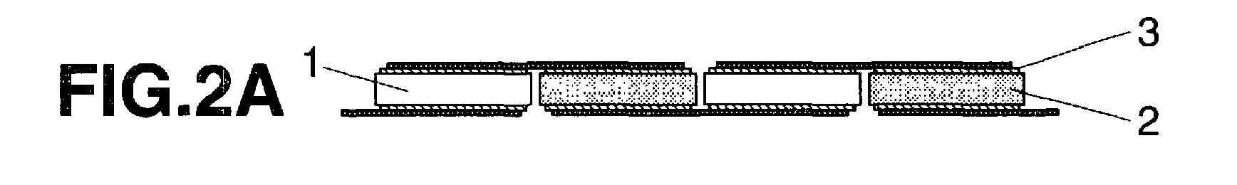
- FIGS. 1a and 2a are cross-sectional views
- FIGS. 1b and 2b are plan views as viewed from the light-receiving surface side. Illustrated in FIGS. 1 and 2 are first solar cells 1 having a first conductivity type substrate, second solar cells 2 having a second conductivity type substrate, bus-bar electrodes 3, and tab wires 4.
- the conventional solar cell module of FIG. 1 consists of solar cells having a first conductivity type substrate.
- the bus-bar electrode on the light-receiving surface side and the bus-bar electrode on the non-light-receiving surface side are connected by tab wires to achieve series connection.
- the solar cell module of the invention shown in FIG. 2 is constructed such that solar cells 1 having a first conductivity type substrate and solar cells 2 having a second conductivity type substrate are alternately arranged.
- cells having electrodes of first polarity and cells having electrodes of second polarity are juxtaposed on a common plane, allowing electrodes on the light-receiving surface or electrodes on the non-light-receiving surface to be connected to each other by tab wires to achieve series connection.
- adjacent cells may be closely arranged at a spacing of 3.0 mm or less, especially 1.0 mm or less.
- the spacing between the enclosure frame and the solar cell at the module periphery is preferably 0.1 to 3.0 mm, more preferably 0.1 to 1.0 mm. If the frame spacing is too narrow, the frame may overlap the solar cell to invite a shadow loss, resulting in a lowering of module conversion efficiency. If the frame spacing is too broad, the packing density of solar cells relative to the area of the solar cell module may be reduced, resulting in a lowering of module conversion efficiency. It is noted that tab wires may be connected with solder or the like by the standard technique.
- FIG. 3 illustrates an exemplary interconnection of an overall conventional solar cell module
- FIG. 4 illustrates an exemplary interconnection of an overall solar cell module according to the invention.
- solar cells are arranged in plural rows of 4 cells by 4 cells and connected in series. Illustrated in FIGS. 3 and 4 are first solar cells 1 having a first conductivity type substrate, second solar cells 2 having a second conductivity type substrate, termini 5 of first polarity electrodes, termini 6 of second polarity electrodes, and an enclosure frame 7. It is appreciated from a comparison between FIGS. 3 and 4 that the inventive solar cell module has a higher packing density of cells relative to the module area than the conventional solar cell module.
- the solar cell module includes a section wherein the first and second solar cells are connected in series.
- the number of first solar cells having first conductivity type substrate is preferably 50% to 70%, more preferably 50% to 60%
- the number of second solar cells having second conductivity type substrate is preferably 30% to 50%, more preferably 40% to 50%. If the number of either one of first and second solar cells is extremely high, then the series connection wiring taking advantage of the invention may be impossible.
- a difference in short-circuit current density between the first and second solar cells is preferably up to 20%, more preferably up to 10%.
- the solar cell module has a short-circuit current density which may be limited to the lowest short-circuit current density among the series connected cells.
- Example and Comparative Example are given below by way of illustration, but the invention is not limited thereto.
- characteristics short-circuit current density, open voltage, fill factor, and conversion efficiency
- a solar simulator light intensity 1 kW/m 2 , spectrum AM 1.5 global.
- a solar cell module of the structure shown in FIG. 4 was fabricated as follows. Solar cells were prepared using n-type single crystal silicon substrate as the first conductivity type substrate and p-type single crystal silicon substrate as the second conductivity type substrate. All the cells thus prepared had a size of 100 mm square. The average characteristics of the solar cells using n-type substrate included a short-circuit current density of 35.1 mA/cm 2 , an open voltage of 0.619 V, a fill factor of 78.3%, and a conversion efficiency of 17.0%.
- the average characteristics of the solar cells using p-type substrate included a short-circuit current density of 35.1 mA/cm 2 , an open voltage of 0.618 V, a fill factor of 78.5%, and a conversion efficiency of 17.0%. Since solar cells were to be connected in series to construct a solar cell module, the solar cells were adjusted, during preparation, so as to have an equivalent short-circuit current density among other characteristics.
- a solar cell module was fabricated within the scope of the invention.
- the spacing between solar cells was 0.5 mm
- the spacing between the cell at the module periphery and the frame was 1.0 mm
- the frame had a width of 5.0 mm.
- tab wires projected 3.0 mm from the cell located at the module periphery in the bus-bar direction, they were connected to bus-bar electrodes of the next row.
- the module thus fabricated had a size of 413.5 mm long by 419.5 mm wide including the frame.
- the solar cell module thus fabricated was characterized by a short-circuit current flow of 3.50 A, an open voltage of 9.88 V, a fill factor of 77.9%, and a conversion efficiency of 15.5%. Notably, no failure at the cell edge was observed although the spacing between solar cells was 0.5 mm.
Landscapes
- Photovoltaic Devices (AREA)
Abstract
Description
- This invention relates to a solar cell module comprising solar cells in the form of semiconductor devices.
- A solar cell module fabricated from crystalline solar cells is generally manufactured by providing solar cells based solely on substrates of one conductivity type and connecting the cells in series for the purpose of increasing the voltage. In this event, if cells each have an electrode of first polarity on a light-receiving surface side and an electrode of second polarity (opposite to the first polarity) on a non-light-receiving surface side are used, then the electrode of first polarity on the light-receiving surface side must be connected to the electrode of second polarity on the non-light-receiving surface side by a conductor containing solder and other components (referred to as "tab wire") in order to achieve series connection. Those electrodes which are connected by the tab wire are electrodes of a relatively large width (about 1 to 3 mm) and generally known as bus-bar electrodes.
- In the conventional solar cell module mentioned above, an attempt is made to arrange solar cells as closely as possible to each other in order to increase the module conversion efficiency. However, because of the presence of the tab wire connecting the electrodes on the light-receiving and non-light-receiving surface sides, an attempt to reduce the spacing between solar cells to a distance of 3.0 mm or less encounters a problem of cell edge failure due to the bending stress of the tab wire. This causes a reduction of the packing density of solar cells relative to the area of the solar cell module.
- One approach to this problem is by reducing the thickness of the tab wire itself simply for the purpose of reducing the bending stress of the tab wire, although another problem of increased wiring resistance arises. Another approach is described, for example, in
JP-A 2008-147260 - This method, however, has drawbacks that a tab wire having a special bent portion must be prepared, and the presence of the bent portion increases the connection length of the tab wire, thus exacerbating the fill factor of the solar cell module.
-
- Patent Document 1:
JP-A 2008-147260 - An object of the invention, which has been made under the aforementioned circumstances, is to provide a solar cell module which is improved in module conversion efficiency by increasing the packing density of solar cells relative to the area of the solar cell module.
- Making extensive investigations to attain the above object, the inventors have found that when a first solar cell comprising a substrate of first conductivity type having a light-receiving surface and a non-light-receiving surface and electrodes of opposite polarity formed on the light-receiving and non-light-receiving surfaces, respectively, and a second solar cell comprising a substrate of second conductivity type opposite to the first conductivity type having a light-receiving surface and a non-light-receiving surface and electrodes of opposite polarity formed on the light-receiving and non-light-receiving surfaces, respectively, are alternately arranged, a solar cell module is constructed in which the first solar cell having an electrode of first polarity and the second solar cell having an electrode of second polarity opposite to the first polarity are juxtaposed in a common plane. This arrangement ensures that the first and second solar cells are connected in series by connecting the electrodes on the light-receiving surface to each other and the electrodes on the non-light-receiving surface to each other with tab wires, and the cells are closely arranged at a spacing of 3.0 mm or less, whereby the packing density of solar cells relative to the area of the solar cell module may be increased, leading to improved module conversion efficiency. The arrangement facilitates attachment of the tab wires and eliminates the stress due to the tab wires, preventing cell edge failure and increasing the yield of manufacture, which ensures fabrication of a highly reliable solar cell module. The invention is predicated on these findings.
It is noted that of the electrodes on the light-receiving and non-light-receiving surfaces, thin electrodes of about 50 to 200 µm wide which are formed on the solar cell front surface across bus-bar electrodes for collecting outputs are referred to as "finger electrodes", and relatively thick electrodes of about 1 to 3 mm wide for taking out the output collected by the finger electrodes are referred to as "bus-bar electrodes". - Accordingly, the invention provides a solar cell module as defined below.
- Claim 1:
- A solar cell module comprising, in an alternating arrangement, a first solar cell comprising a first conductivity type substrate having a light-receiving surface and a non-light-receiving surface and electrodes of opposite polarity formed on the light-receiving and non-light-receiving surfaces, respectively, and a second solar cell comprising a second conductivity type substrate having a light-receiving surface and a non-light-receiving surface and electrodes of opposite polarity formed on the light-receiving and non-light-receiving surfaces, respectively.
- Claim 2:
- The solar cell module of
claim 1, including a section wherein the first and second solar cells are connected in series, wherein the number of first solar cells used in the series connection section is 50% to 70%, and the number of second solar cells used in the series connection section is 30% to 50%.
- The solar cell module of
- Claim 3:
- The solar cell module of
claim
- The solar cell module of
- Claim 4:
- The solar cell module of
claim
- The solar cell module of
- Claim 5:
- The solar cell module of any one of
claims 1 to 4 wherein a difference in short-circuit current density between the first and second solar cells is up to 20%.
- The solar cell module of any one of
- The solar cell arrangement and interconnecting method according to the invention permit the packing density of solar cells relative to the area of the solar cell module to be increased, whereby the module conversion efficiency is improved. Additionally, since the stress applied from tab wires to the edge of solar cells can be reduced as compared with the prior art method, a highly reliable solar cell module can be fabricated in improved manufacture yields.
-
-
FIG. 1 illustrates an exemplary series connection of solar cells in a prior art solar cell module,FIG. 1a being a cross-sectional view andFIG. 1b being a plan view of the light-receiving surface side. -
FIG. 2 illustrates an exemplary series connection of solar cells in a solar cell module according to the invention,FIG. 2a being a cross-sectional view andFIG. 2b being a plan view of the light-receiving surface side. -
FIG. 3 is a plan view of the light-receiving surface side, showing an exemplary interconnection of an overall prior art solar cell module. -
FIG. 4 is a plan view of the light-receiving surface side, showing an exemplary interconnection of an overall solar cell module according to the invention. - Now, embodiments of the invention are described in detail with reference to the drawings although the invention is not limited to the illustrated embodiments. Throughout the drawings for illustrating embodiments, like characters represent parts having the same function and iteration of their description is omitted. For ease of understanding, drawing is made in exaggeration with respect to the spacing between solar cells and the thickness thereof. For convenience sake, finger electrodes are omitted.
- The invention is directed to a solar cell module in which a first solar cell(s) comprising a first conductivity type substrate having a light-receiving surface and a non-light-receiving surface and electrodes of opposite polarity formed on the light-receiving and non-light-receiving surfaces, respectively, and a second solar cell(s) comprising a second conductivity type substrate having a light-receiving surface and a non-light-receiving surface and electrodes of opposite polarity formed on the light-receiving and non-light-receiving surfaces, respectively, are alternately arranged. This solar cell module is constructed as shown in
FIG. 2 whereinsolar cells 1 having a first conductivity type substrate andsolar cells 2 having a second conductivity type substrate are alternately arranged, and bus-bar electrodes 3 are connected bytab wires 4. Herein, the conductivity type of the substrate of the first solar cell is opposite to the conductivity type of the substrate of the second solar cell. For example, when the former is n-type, the latter is p-type. Also, the polarity of the electrode on the light-receiving surface of the substrate of the first solar cell is identical with the polarity of the electrode on the non-light-receiving surface of the substrate of the second solar cell, while the electrode on the non-light-receiving surface of the substrate of the first solar cell and the electrode on the light-receiving surface of the substrate of the second solar cell are of the same polarity. In the embodiment of the invention, as shown inFIG. 2b , for example, when the first solar cell is disposed with the light-receiving surface of its substrate facing upward, the second solar cell is disposed with the light-receiving surface of its substrate facing upward, so that the electrode on the light-receiving surface of the first solar cell and the electrode on the light-receiving surface of the second solar cell may be linearly connected in a common plane without a bend. - In this embodiment, the conductivity type of substrate, impurity diffusion layer, antireflective coating and other components of the solar cells used herein may be in accord with well-known examples. The solar cells may be prepared by the well-known method described in
JP-A 2001-77386 - The semiconductor substrate of which the solar cells are constructed according to the invention may be, for example, a p- or n-type single crystal silicon substrate, p-or n-type polycrystalline silicon substrate, non-silicon compound semiconductor substrate or the like. For the single crystal silicon substrate, as-cut single crystal {100} p-type silicon substrates in which high purity silicon is doped with a Group III element such as boron or gallium to provide a resistivity of 0.1 to 5 Ω-cm may be used. Similar n-type silicon substrates doped with a Group V element such as phosphorus, antimony or arsenic are also useful.
- With respect to the purity of the single crystal silicon substrate used herein, substrates with a lower concentration of metal impurities such as iron, aluminum and titanium are preferred in that higher efficiency solar cells can be fabricated using longer lifetime substrates. The single crystal silicon substrate may be prepared by any methods including the CZ and FZ methods. Herein, metallic grade silicon which is previously purified by a well-known process such as the Siemens process may also be used in the above method.
- The thickness of semiconductor substrate is preferably 100 to 300 µm, and more preferably 150 to 250 µm, for a balance of the cost and yield of substrate, and conversion efficiency. If the resistivity of semiconductor substrate is lower than the above-defined range, the distribution of conversion efficiency of solar cells may become narrower, but the crystal cost may be high because of a limitation on ingot pulling. If the resistivity is higher than the range, the distribution of conversion efficiency of solar cells may become broader, but the crystal cost may be low.
- In the embodiment of the invention, the first conductivity type may be either n-type or p-type. The second conductivity type may be p-type when n-type is selected for the first conductivity type, or n-type when p-type is selected for the first conductivity type.
- Additionally, the substrate surface is preferably provided with microscopic asperities known as "texture." The texture is an effective means for reducing the surface reflectance of solar cells. The texture may be readily provided by dipping in a hot alkali aqueous solution such as sodium hydroxide.
- As to the impurity diffusion layer, the impurity source used may be selected from Group V elements such as phosphorus, arsenic and antimony and Group III elements such as boron, aluminum and gallium. In one example, an impurity diffusion layer may be formed by the vapor phase diffusion process using phosphorus oxychloride for phosphorus diffusion, for instance. In this example, heat treatment is preferably carried out in an atmosphere of phosphorus oxychloride or the like at 850 to 900°C for 20 to 40 minutes. Also preferably the impurity diffusion layer has a thickness of 0.1 to 3.0 µm, and more preferably 0.5 to 2.0 µm. If the impurity diffusion layer is too thick, there may be available more sites where electrons and holes generated are recombined, leading to a lowering of conversion efficiency. If the impurity diffusion layer is too thin, there are less sites where electrons and holes generated are recombined, but the transverse flow resistance of current flowing through the substrate to the collector electrode may be increased, leading to a lowering of conversion efficiency. Diffusion of boron, for example, may be effected by applying a commercially available boron-containing coating agent, drying, and heat treating at 900 to 1050°C for 20 to 60 minutes to form a diffusion layer.
- In conventional silicon solar cells, a p-n junction must be formed solely on the light-receiving surface. To this end, a suitable means for avoiding formation of p-n junction on the back surface is preferably employed, for example, by stacking two substrates together prior to diffusion, or by forming a SiO2 film or SiNx film as a diffusion mask on the back surface prior to diffusion. Besides the vapor phase diffusion method, the impurity diffusion layer may also be formed by another technique such as screen printing or spin coating.
- The antireflective film is preferably a SiNx film formed using a plasma CVD system or the like, or a multilayer film including a SiO2 film resulting from thermal oxidation and a SiNx film formed as above. Its thickness is preferably 70 to 100 nm.
- On the semiconductor substrate thus obtained, electrodes are formed using the screen printing technique or the like. The shape of electrodes is not particularly limited. The width of bus-bar electrodes is typically 1 to 3 mm, and the number of bus-bar electrodes is preferably 1 to 4, and more preferably 2 to 3 on each surface. Where a plurality of electrodes are formed on one surface, the electrodes are preferably formed to extend parallel to each other.
- In the screen printing technique, a conductive paste obtained by mixing conductive particles such as aluminum powder or silver powder, glass frit, organic binder and the like is screen printed. After printing, the paste is baked at 700 to 800°C for 5 to 30 minutes to form electrodes. Electrode formation by the printing technique is preferred although electrodes may also be prepared by evaporation and sputtering techniques. Moreover, electrodes on the light-receiving and non-light-receiving surfaces may be baked at a time. In this way, an electrode of first polarity is formed on the light-receiving surface of the first solar cell having a first conductivity type substrate and an electrode of second polarity opposite to the first polarity is formed on the non-light-receiving surface of the first solar cell. Similarly, an electrode of second polarity is formed on the light-receiving surface of the second solar cell having a second conductivity type substrate and an electrode of first polarity is formed on the non-light-receiving surface of the second solar cell. In an example wherein a n-type semiconductor substrate is selected as the first conductivity type substrate and a p-type semiconductor substrate is selected as the second conductivity type substrate, the electrode of first polarity is a negative electrode and the electrode of second polarity is a positive electrode.
- In the solar cell module of the invention, at least one first solar cell and at least one second solar cell, both defined as above, are alternately connected in series and/or in parallel. The thus connected solar cells may be encapsulated with a transparent resin such as ethylene-vinyl acetate (EVA) copolymer, to complete a solar cell module. Moreover, the module may be formed to any of a protected structure which is formed using a substrate as in conventional modules or a film as in conventional modules along with the encapsulating resin, a super-straight structure, a substrate structure, and a glass package structure. Additionally, a frame may be attached for providing protection around the module. Such a solar cell module may be manufactured by any well-known methods, for example, the method of
JP-A H09-51117 - One preferred embodiment of the solar cell module of the invention is described in detail with reference to the drawings.
FIG. 1 illustrates an exemplary series connection of solar cells in a conventional solar cell module, andFIG. 2 illustrates an exemplary series connection of solar cells in a solar cell module according to the invention.FIGS. 1a and 2a are cross-sectional views, andFIGS. 1b and 2b are plan views as viewed from the light-receiving surface side. Illustrated inFIGS. 1 and 2 are firstsolar cells 1 having a first conductivity type substrate, secondsolar cells 2 having a second conductivity type substrate, bus-bar electrodes 3, andtab wires 4. - The conventional solar cell module of
FIG. 1 consists of solar cells having a first conductivity type substrate. As such, the bus-bar electrode on the light-receiving surface side and the bus-bar electrode on the non-light-receiving surface side are connected by tab wires to achieve series connection. An attempt to arrange solar cells as closely as possible for the purpose of increasing the module conversion efficiency can result in a cell edge failure due to the bending stress of tab wires. - On the other hand, the solar cell module of the invention shown in
FIG. 2 is constructed such thatsolar cells 1 having a first conductivity type substrate andsolar cells 2 having a second conductivity type substrate are alternately arranged. Thus cells having electrodes of first polarity and cells having electrodes of second polarity are juxtaposed on a common plane, allowing electrodes on the light-receiving surface or electrodes on the non-light-receiving surface to be connected to each other by tab wires to achieve series connection. As a result, adjacent cells may be closely arranged at a spacing of 3.0 mm or less, especially 1.0 mm or less. If the spacing between cells is too large, the packing density of solar cells relative to the area of the solar cell module may be reduced, resulting in a lowering of module conversion efficiency. Although a shorter spacing between cells is desirable, a spacing of at least 0.1 mm is preferred because a too close spacing allows for contact between cells, causing fissure or chipping. In another embodiment wherein an enclosure frame is attached, the spacing between the enclosure frame and the solar cell at the module periphery (outermost row) is preferably 0.1 to 3.0 mm, more preferably 0.1 to 1.0 mm. If the frame spacing is too narrow, the frame may overlap the solar cell to invite a shadow loss, resulting in a lowering of module conversion efficiency. If the frame spacing is too broad, the packing density of solar cells relative to the area of the solar cell module may be reduced, resulting in a lowering of module conversion efficiency. It is noted that tab wires may be connected with solder or the like by the standard technique. - Next,
FIG. 3 illustrates an exemplary interconnection of an overall conventional solar cell module, andFIG. 4 illustrates an exemplary interconnection of an overall solar cell module according to the invention. In the illustrated example, solar cells are arranged in plural rows of 4 cells by 4 cells and connected in series. Illustrated inFIGS. 3 and 4 are firstsolar cells 1 having a first conductivity type substrate, secondsolar cells 2 having a second conductivity type substrate,termini 5 of first polarity electrodes,termini 6 of second polarity electrodes, and anenclosure frame 7. It is appreciated from a comparison betweenFIGS. 3 and 4 that the inventive solar cell module has a higher packing density of cells relative to the module area than the conventional solar cell module. - In the preferred embodiment, the solar cell module includes a section wherein the first and second solar cells are connected in series. In the series connection section, the number of first solar cells having first conductivity type substrate is preferably 50% to 70%, more preferably 50% to 60%, and the number of second solar cells having second conductivity type substrate is preferably 30% to 50%, more preferably 40% to 50%. If the number of either one of first and second solar cells is extremely high, then the series connection wiring taking advantage of the invention may be impossible.
- Moreover, a difference in short-circuit current density between the first and second solar cells is preferably up to 20%, more preferably up to 10%. With a too much difference in short-circuit current density, the solar cell module has a short-circuit current density which may be limited to the lowest short-circuit current density among the series connected cells.
- Example and Comparative Example are given below by way of illustration, but the invention is not limited thereto.
In Examples below, characteristics (short-circuit current density, open voltage, fill factor, and conversion efficiency) of a solar cell and a solar cell module were measured using a solar simulator (light intensity 1 kW/m2, spectrum AM 1.5 global). - In this Example, a solar cell module of the structure shown in
FIG. 4 was fabricated as follows.
Solar cells were prepared using n-type single crystal silicon substrate as the first conductivity type substrate and p-type single crystal silicon substrate as the second conductivity type substrate. All the cells thus prepared had a size of 100 mm square.
The average characteristics of the solar cells using n-type substrate included a short-circuit current density of 35.1 mA/cm2, an open voltage of 0.619 V, a fill factor of 78.3%, and a conversion efficiency of 17.0%.
The average characteristics of the solar cells using p-type substrate included a short-circuit current density of 35.1 mA/cm2, an open voltage of 0.618 V, a fill factor of 78.5%, and a conversion efficiency of 17.0%.
Since solar cells were to be connected in series to construct a solar cell module, the solar cells were adjusted, during preparation, so as to have an equivalent short-circuit current density among other characteristics. - Using the solar cells of two types in an array of 4x4 = 16, a solar cell module was fabricated within the scope of the invention. The spacing between solar cells was 0.5 mm, the spacing between the cell at the module periphery and the frame was 1.0 mm, and the frame had a width of 5.0 mm. While tab wires projected 3.0 mm from the cell located at the module periphery in the bus-bar direction, they were connected to bus-bar electrodes of the next row.
The module thus fabricated had a size of 413.5 mm long by 419.5 mm wide including the frame.
The solar cell module thus fabricated was characterized by a short-circuit current flow of 3.50 A, an open voltage of 9.88 V, a fill factor of 77.9%, and a conversion efficiency of 15.5%.
Notably, no failure at the cell edge was observed although the spacing between solar cells was 0.5 mm. - In Comparative Example, a solar cell module of the structure shown in
FIG. 3 was fabricated as follows.
As the solar cells, only those cells using the first conductivity type substrate in Example 1 were used in an array of 4×4 = 16. With respect to the spacing between solar cells, the spacing for interconnection by tab wires in bus-bar direction was 4.0 mm, and the spacing without interconnection by tab wires was 0.5 mm. The remaining parameters including the spacing between the cell at the module periphery and the frame, the frame width, and the projection of tab wires from the cell at the module periphery in the bus-bar direction were the same as in Example 1.
The module thus fabricated had a size of 413.5 mm long by 430 mm wide including the frame.
The solar cell module fabricated in Comparative Example was characterized by a short-circuit current flow of 3.51 A, an open voltage of 9.90 V, a fill factor of 77.4%, and a conversion efficiency of 15.2%. -
- 1
- first solar cell using first conductivity type substrate
- 2
- second solar cell using second conductivity type substrate
- 3
- bus-bar electrode
- 4
- tab wire
- 5
- terminus of first polarity electrode
- 6
- terminus of second polarity electrode
- 7
- enclosure frame
Claims (5)
- A solar cell module comprising, in an alternating arrangement, a first solar cell comprising a first conductivity type substrate having a light-receiving surface and a non-light-receiving surface and electrodes of opposite polarity formed on the light-receiving and non-light-receiving surfaces, respectively, and a second solar cell comprising a second conductivity type substrate having a light-receiving surface and a non-light-receiving surface and electrodes of opposite polarity formed on the light-receiving and non-light-receiving surfaces, respectively.
- The solar cell module of claim 1, including a section wherein the first and second solar cells are connected in series, wherein the number of first solar cells used in the series connection section is 50% to 70%, and the number of second solar cells used in the series connection section is 30% to 50%.
- The solar cell module of claim 1 or 2 wherein the first conductivity type substrate is a n-type semiconductor substrate and the second conductivity type substrate is a p-type semiconductor substrate.
- The solar cell module of claim 1, 2 or 3 wherein the solar cells are arranged at a spacing of 0.1 mm to 3.0 mm.
- The solar cell module of any one of claims 1 to 4 wherein a difference in short-circuit current density between the first and second solar cells is up to 20%.
Applications Claiming Priority (2)
| Application Number | Priority Date | Filing Date | Title |
|---|---|---|---|
| JP2009033843 | 2009-02-17 | ||
| PCT/JP2010/052320 WO2010095634A1 (en) | 2009-02-17 | 2010-02-17 | Solar battery module |
Publications (3)
| Publication Number | Publication Date |
|---|---|
| EP2400560A1 true EP2400560A1 (en) | 2011-12-28 |
| EP2400560A4 EP2400560A4 (en) | 2017-03-08 |
| EP2400560B1 EP2400560B1 (en) | 2020-03-25 |
Family
ID=42633914
Family Applications (1)
| Application Number | Title | Priority Date | Filing Date |
|---|---|---|---|
| EP10743760.0A Active EP2400560B1 (en) | 2009-02-17 | 2010-02-17 | Solar battery module |
Country Status (12)
| Country | Link |
|---|---|
| US (1) | US20120103386A1 (en) |
| EP (1) | EP2400560B1 (en) |
| JP (1) | JPWO2010095634A1 (en) |
| KR (1) | KR101733687B1 (en) |
| CN (1) | CN102356471B (en) |
| AU (1) | AU2010216750B2 (en) |
| ES (1) | ES2785221T3 (en) |
| MY (1) | MY159905A (en) |
| RU (1) | RU2526894C2 (en) |
| SG (1) | SG173708A1 (en) |
| TW (1) | TWI493732B (en) |
| WO (1) | WO2010095634A1 (en) |
Cited By (1)
| Publication number | Priority date | Publication date | Assignee | Title |
|---|---|---|---|---|
| WO2016012626A1 (en) * | 2014-07-25 | 2016-01-28 | Commissariat A L'energie Atomique Et Aux Energies Alternatives | Photovoltaic module comprising a plurality of bifacial cells and method for producing such a module |
Families Citing this family (14)
| Publication number | Priority date | Publication date | Assignee | Title |
|---|---|---|---|---|
| KR101372050B1 (en) * | 2011-11-10 | 2014-03-10 | 엘지이노텍 주식회사 | Solar cell module and the manufacturing method thereof |
| CN104364080B (en) * | 2012-06-05 | 2017-06-23 | 法国圣戈班玻璃厂 | Top-sheet with integrated photovoltaic module |
| DE102012211008A1 (en) | 2012-06-27 | 2014-01-02 | Robert Bosch Gmbh | Battery with mechanically interconnected battery cells |
| US20150194551A1 (en) * | 2014-01-09 | 2015-07-09 | Emcore Solar Power, Inc. | Solar cell array having two different types of cells |
| EP2919275B1 (en) * | 2014-03-13 | 2021-08-18 | Airbus Defence and Space GmbH | Solar cell interconnector, solar cell array and method of interconnecting solar cells of a solar cell array |
| CN104701415A (en) * | 2015-02-13 | 2015-06-10 | 晶澳(扬州)太阳能科技有限公司 | Manufacture method for solar cell module via solar cells different in structure |
| KR102583243B1 (en) | 2015-10-08 | 2023-09-27 | 한국과학기술원 | A method for guiding based on augmented reality using mobile device |
| CN106784052A (en) * | 2017-02-10 | 2017-05-31 | 泰州中来光电科技有限公司 | A kind of solar cell module |
| CN111755569A (en) * | 2020-06-17 | 2020-10-09 | 无锡先导智能装备股份有限公司 | Battery string preparation method |
| JP2022152850A (en) * | 2021-03-29 | 2022-10-12 | 出光興産株式会社 | panel module |
| CN116995123B (en) * | 2023-08-17 | 2024-10-29 | 隆基绿能科技股份有限公司 | Back contact battery string and photovoltaic module |
| KR20250052604A (en) | 2023-10-12 | 2025-04-21 | 주식회사스페이스엘비스 | Method for provide multi-sensory feedback using augmented reality and apparatus and system therefor |
| KR102949634B1 (en) | 2023-10-12 | 2026-04-07 | 주식회사스페이스엘비스 | POI-based integrated information provision method using mixed reality and apparatus and system therefor |
| TW202518607A (en) * | 2023-10-30 | 2025-05-01 | 強茂股份有限公司 | Manufacturing method of pre-molded packaging lead frame |
Family Cites Families (17)
| Publication number | Priority date | Publication date | Assignee | Title |
|---|---|---|---|---|
| US3370986A (en) * | 1963-12-10 | 1968-02-27 | Westinghouse Electric Corp | Photovoltaic series array comprising p/n and n/p cells |
| DE3124581A1 (en) * | 1980-09-26 | 1982-05-19 | Licentia Patent-Verwaltungs-Gmbh, 6000 Frankfurt | SOLAR CELL ARRANGEMENT |
| US4467438A (en) * | 1982-01-18 | 1984-08-21 | Dset Laboratories, Inc. | Method and apparatus for determining spectral response and spectral response mismatch between photovoltaic devices |
| US4746618A (en) * | 1987-08-31 | 1988-05-24 | Energy Conversion Devices, Inc. | Method of continuously forming an array of photovoltaic cells electrically connected in series |
| JP3437885B2 (en) | 1995-05-31 | 2003-08-18 | シャープ株式会社 | Solar cell module and method of manufacturing the same |
| JP3679611B2 (en) * | 1998-06-05 | 2005-08-03 | 三洋電機株式会社 | Solar cell module |
| JP2000315811A (en) * | 1999-04-30 | 2000-11-14 | Sekisui Jushi Co Ltd | Method for connecting solar cells in series and solar cell module |
| JP4812147B2 (en) | 1999-09-07 | 2011-11-09 | 株式会社日立製作所 | Manufacturing method of solar cell |
| JP2002026361A (en) * | 2000-07-07 | 2002-01-25 | Hitachi Ltd | Double-sided photovoltaic module |
| AU2002238953B2 (en) * | 2001-03-19 | 2007-03-29 | Shin-Etsu Chemical Co., Ltd | Solar cell and its manufacturing method |
| AU2002252110A1 (en) * | 2002-02-27 | 2003-09-09 | Midwest Research Institute | Monolithic photovoltaic energy conversion device |
| KR101126059B1 (en) * | 2004-09-03 | 2012-04-12 | 신에쯔 한도타이 가부시키가이샤 | Photovoltaic power generation module and photovoltaic power generation system employing it |
| JP5084146B2 (en) * | 2006-01-30 | 2012-11-28 | 三洋電機株式会社 | Photovoltaic module |
| DE102006021804A1 (en) * | 2006-05-09 | 2007-11-15 | International Solar Energy Research Center Konstanz E.V. | Solar cell module and method for the production of solar cell modules |
| JP5153097B2 (en) * | 2006-07-31 | 2013-02-27 | 三洋電機株式会社 | Solar cell module |
| JP2008147260A (en) | 2006-12-06 | 2008-06-26 | Sharp Corp | Interconnector, solar cell string, solar cell module, and solar cell module manufacturing method |
| JP5507034B2 (en) * | 2007-03-01 | 2014-05-28 | 三洋電機株式会社 | Solar cell module and manufacturing method thereof |
-
2010
- 2010-02-11 TW TW099104442A patent/TWI493732B/en active
- 2010-02-17 JP JP2011500618A patent/JPWO2010095634A1/en active Pending
- 2010-02-17 ES ES10743760T patent/ES2785221T3/en active Active
- 2010-02-17 KR KR1020117020737A patent/KR101733687B1/en active Active
- 2010-02-17 SG SG2011058815A patent/SG173708A1/en unknown
- 2010-02-17 CN CN201080011928.XA patent/CN102356471B/en active Active
- 2010-02-17 US US13/201,792 patent/US20120103386A1/en not_active Abandoned
- 2010-02-17 EP EP10743760.0A patent/EP2400560B1/en active Active
- 2010-02-17 WO PCT/JP2010/052320 patent/WO2010095634A1/en not_active Ceased
- 2010-02-17 RU RU2011138163/28A patent/RU2526894C2/en active
- 2010-02-17 AU AU2010216750A patent/AU2010216750B2/en not_active Ceased
- 2010-02-17 MY MYPI2011003737A patent/MY159905A/en unknown
Non-Patent Citations (1)
| Title |
|---|
| See references of WO2010095634A1 * |
Cited By (3)
| Publication number | Priority date | Publication date | Assignee | Title |
|---|---|---|---|---|
| WO2016012626A1 (en) * | 2014-07-25 | 2016-01-28 | Commissariat A L'energie Atomique Et Aux Energies Alternatives | Photovoltaic module comprising a plurality of bifacial cells and method for producing such a module |
| FR3024283A1 (en) * | 2014-07-25 | 2016-01-29 | Commissariat Energie Atomique | PHOTOVOLTAIC MODULE COMPRISING A PLURALITY OF BIFACIAL CELLS AND METHOD OF MANUFACTURING SUCH A MODULE |
| US10693026B2 (en) | 2014-07-25 | 2020-06-23 | Commissariat A L'energie Atomique Et Aux Energies Alternatives | Photovoltaic module comprising a plurality of bifacial cells and method for producing such a module |
Also Published As
| Publication number | Publication date |
|---|---|
| RU2526894C2 (en) | 2014-08-27 |
| JPWO2010095634A1 (en) | 2012-08-23 |
| EP2400560A4 (en) | 2017-03-08 |
| KR101733687B1 (en) | 2017-05-11 |
| CN102356471A (en) | 2012-02-15 |
| EP2400560B1 (en) | 2020-03-25 |
| ES2785221T3 (en) | 2020-10-06 |
| KR20110122176A (en) | 2011-11-09 |
| TW201101509A (en) | 2011-01-01 |
| TWI493732B (en) | 2015-07-21 |
| CN102356471B (en) | 2015-11-25 |
| WO2010095634A1 (en) | 2010-08-26 |
| AU2010216750B2 (en) | 2014-11-27 |
| US20120103386A1 (en) | 2012-05-03 |
| RU2011138163A (en) | 2013-03-27 |
| MY159905A (en) | 2017-02-15 |
| SG173708A1 (en) | 2011-09-29 |
| AU2010216750A1 (en) | 2011-09-01 |
Similar Documents
| Publication | Publication Date | Title |
|---|---|---|
| EP2400560B1 (en) | Solar battery module | |
| US9455360B2 (en) | Method of fabricating a metal wrap through solar cell | |
| EP3503207B1 (en) | Solar cell module | |
| EP2757591B1 (en) | Solar cell module | |
| EP2522031B1 (en) | Solar panel module and method for manufacturing such a solar panel module | |
| KR101554045B1 (en) | Solar cell module | |
| US9608140B2 (en) | Solar cell and solar cell module | |
| US20160197207A1 (en) | Solar cell, solar cell module, and manufacturing method of solar cell | |
| EP2916361B1 (en) | Solar cell and solar cell module | |
| JP4578123B2 (en) | Solar cell module | |
| JP2015159276A (en) | Solar battery element, and solar battery module | |
| CN103155161B (en) | Photovoltaic devices and manufacture method thereof | |
| JP2015207598A (en) | Solar cell module, solar cell, and inter-element connection body | |
| EP2605285A2 (en) | Photovoltaic device | |
| US20140210073A1 (en) | Conductive paste, electrode for semiconductor device, semiconductor device, and method for manufacturing semiconductor device | |
| JP2015230985A (en) | SOLAR CELL, ITS MANUFACTURING METHOD, SOLAR CELL PANEL | |
| CN102484146A (en) | Solar cell | |
| JP4953562B2 (en) | Solar cell module | |
| JP2010192572A (en) | Solar cell, and solar cell module | |
| JP2006013173A (en) | Solar cell module | |
| EP3125300B1 (en) | Solar cell and solar cell module using same | |
| KR20190056550A (en) | Solar cell module with Metal Wrap Through type solar cell and wire interconnector | |
| JP2016178280A (en) | Solar cell element and solar cell module using the same | |
| JP5501549B2 (en) | Photoelectric conversion element and photoelectric conversion module composed thereof | |
| JP2010267990A (en) | Solar cell element and solar cell module |
Legal Events
| Date | Code | Title | Description |
|---|---|---|---|
| PUAI | Public reference made under article 153(3) epc to a published international application that has entered the european phase |
Free format text: ORIGINAL CODE: 0009012 |
|
| 17P | Request for examination filed |
Effective date: 20110831 |
|
| AK | Designated contracting states |
Kind code of ref document: A1 Designated state(s): AT BE BG CH CY CZ DE DK EE ES FI FR GB GR HR HU IE IS IT LI LT LU LV MC MK MT NL NO PL PT RO SE SI SK SM TR |
|
| DAX | Request for extension of the european patent (deleted) | ||
| RA4 | Supplementary search report drawn up and despatched (corrected) |
Effective date: 20170208 |
|
| RIC1 | Information provided on ipc code assigned before grant |
Ipc: H01L 31/042 20140101AFI20170202BHEP |
|
| REG | Reference to a national code |
Ref country code: DE Ref legal event code: R079 Ref document number: 602010063626 Country of ref document: DE Free format text: PREVIOUS MAIN CLASS: H01L0031042000 Ipc: H01L0031020000 |
|
| RIC1 | Information provided on ipc code assigned before grant |
Ipc: H01L 31/02 20060101AFI20190822BHEP Ipc: H01L 31/042 20140101ALI20190822BHEP Ipc: H01L 31/05 20140101ALI20190822BHEP |
|
| GRAP | Despatch of communication of intention to grant a patent |
Free format text: ORIGINAL CODE: EPIDOSNIGR1 |
|
| INTG | Intention to grant announced |
Effective date: 20190927 |
|
| GRAS | Grant fee paid |
Free format text: ORIGINAL CODE: EPIDOSNIGR3 |
|
| GRAA | (expected) grant |
Free format text: ORIGINAL CODE: 0009210 |
|
| STAA | Information on the status of an ep patent application or granted ep patent |
Free format text: STATUS: THE PATENT HAS BEEN GRANTED |
|
| RBV | Designated contracting states (corrected) |
Designated state(s): DE ES FR |
|
| AK | Designated contracting states |
Kind code of ref document: B1 Designated state(s): DE ES FR |
|
| REG | Reference to a national code |
Ref country code: DE Ref legal event code: R096 Ref document number: 602010063626 Country of ref document: DE |
|
| REG | Reference to a national code |
Ref country code: ES Ref legal event code: FG2A Ref document number: 2785221 Country of ref document: ES Kind code of ref document: T3 Effective date: 20201006 |
|
| REG | Reference to a national code |
Ref country code: DE Ref legal event code: R097 Ref document number: 602010063626 Country of ref document: DE |
|
| PLBE | No opposition filed within time limit |
Free format text: ORIGINAL CODE: 0009261 |
|
| STAA | Information on the status of an ep patent application or granted ep patent |
Free format text: STATUS: NO OPPOSITION FILED WITHIN TIME LIMIT |
|
| 26N | No opposition filed |
Effective date: 20210112 |
|
| P01 | Opt-out of the competence of the unified patent court (upc) registered |
Effective date: 20230512 |
|
| REG | Reference to a national code |
Ref country code: DE Ref legal event code: R079 Ref document number: 602010063626 Country of ref document: DE Free format text: PREVIOUS MAIN CLASS: H01L0031020000 Ipc: H10F0077000000 |
|
| PGFP | Annual fee paid to national office [announced via postgrant information from national office to epo] |
Ref country code: FR Payment date: 20251231 Year of fee payment: 17 |
|
| PGFP | Annual fee paid to national office [announced via postgrant information from national office to epo] |
Ref country code: ES Payment date: 20260304 Year of fee payment: 17 |
|
| PGFP | Annual fee paid to national office [announced via postgrant information from national office to epo] |
Ref country code: DE Payment date: 20251230 Year of fee payment: 17 |