EP2410582A2 - Dispositif électroluminescent de type tige et son procédé de fabrication - Google Patents
Dispositif électroluminescent de type tige et son procédé de fabrication Download PDFInfo
- Publication number
- EP2410582A2 EP2410582A2 EP11186011A EP11186011A EP2410582A2 EP 2410582 A2 EP2410582 A2 EP 2410582A2 EP 11186011 A EP11186011 A EP 11186011A EP 11186011 A EP11186011 A EP 11186011A EP 2410582 A2 EP2410582 A2 EP 2410582A2
- Authority
- EP
- European Patent Office
- Prior art keywords
- layer
- light emitting
- polarity
- rod
- emitting device
- Prior art date
- Legal status (The legal status is an assumption and is not a legal conclusion. Google has not performed a legal analysis and makes no representation as to the accuracy of the status listed.)
- Granted
Links
Images


Classifications
-
- H—ELECTRICITY
- H10—SEMICONDUCTOR DEVICES; ELECTRIC SOLID-STATE DEVICES NOT OTHERWISE PROVIDED FOR
- H10H—INORGANIC LIGHT-EMITTING SEMICONDUCTOR DEVICES HAVING POTENTIAL BARRIERS
- H10H20/00—Individual inorganic light-emitting semiconductor devices having potential barriers, e.g. light-emitting diodes [LED]
- H10H20/80—Constructional details
- H10H20/81—Bodies
- H10H20/817—Bodies characterised by the crystal structures or orientations, e.g. polycrystalline, amorphous or porous
- H10H20/818—Bodies characterised by the crystal structures or orientations, e.g. polycrystalline, amorphous or porous within the light-emitting regions
-
- H—ELECTRICITY
- H10—SEMICONDUCTOR DEVICES; ELECTRIC SOLID-STATE DEVICES NOT OTHERWISE PROVIDED FOR
- H10H—INORGANIC LIGHT-EMITTING SEMICONDUCTOR DEVICES HAVING POTENTIAL BARRIERS
- H10H20/00—Individual inorganic light-emitting semiconductor devices having potential barriers, e.g. light-emitting diodes [LED]
- H10H20/01—Manufacture or treatment
- H10H20/011—Manufacture or treatment of bodies, e.g. forming semiconductor layers
- H10H20/018—Bonding of wafers
-
- B—PERFORMING OPERATIONS; TRANSPORTING
- B82—NANOTECHNOLOGY
- B82Y—SPECIFIC USES OR APPLICATIONS OF NANOSTRUCTURES; MEASUREMENT OR ANALYSIS OF NANOSTRUCTURES; MANUFACTURE OR TREATMENT OF NANOSTRUCTURES
- B82Y20/00—Nanooptics, e.g. quantum optics or photonic crystals
-
- H—ELECTRICITY
- H10—SEMICONDUCTOR DEVICES; ELECTRIC SOLID-STATE DEVICES NOT OTHERWISE PROVIDED FOR
- H10H—INORGANIC LIGHT-EMITTING SEMICONDUCTOR DEVICES HAVING POTENTIAL BARRIERS
- H10H20/00—Individual inorganic light-emitting semiconductor devices having potential barriers, e.g. light-emitting diodes [LED]
- H10H20/01—Manufacture or treatment
- H10H20/011—Manufacture or treatment of bodies, e.g. forming semiconductor layers
- H10H20/013—Manufacture or treatment of bodies, e.g. forming semiconductor layers having light-emitting regions comprising only Group III-V materials
- H10H20/0133—Manufacture or treatment of bodies, e.g. forming semiconductor layers having light-emitting regions comprising only Group III-V materials with a substrate not being Group III-V materials
- H10H20/01335—Manufacture or treatment of bodies, e.g. forming semiconductor layers having light-emitting regions comprising only Group III-V materials with a substrate not being Group III-V materials the light-emitting regions comprising nitride materials
-
- H—ELECTRICITY
- H10—SEMICONDUCTOR DEVICES; ELECTRIC SOLID-STATE DEVICES NOT OTHERWISE PROVIDED FOR
- H10H—INORGANIC LIGHT-EMITTING SEMICONDUCTOR DEVICES HAVING POTENTIAL BARRIERS
- H10H20/00—Individual inorganic light-emitting semiconductor devices having potential barriers, e.g. light-emitting diodes [LED]
- H10H20/80—Constructional details
- H10H20/81—Bodies
- H10H20/813—Bodies having a plurality of light-emitting regions, e.g. multi-junction LEDs or light-emitting devices having photoluminescent regions within the bodies
-
- H—ELECTRICITY
- H10—SEMICONDUCTOR DEVICES; ELECTRIC SOLID-STATE DEVICES NOT OTHERWISE PROVIDED FOR
- H10H—INORGANIC LIGHT-EMITTING SEMICONDUCTOR DEVICES HAVING POTENTIAL BARRIERS
- H10H20/00—Individual inorganic light-emitting semiconductor devices having potential barriers, e.g. light-emitting diodes [LED]
- H10H20/80—Constructional details
- H10H20/81—Bodies
- H10H20/819—Bodies characterised by their shape, e.g. curved or truncated substrates
- H10H20/821—Bodies characterised by their shape, e.g. curved or truncated substrates of the light-emitting regions, e.g. non-planar junctions
-
- H—ELECTRICITY
- H10—SEMICONDUCTOR DEVICES; ELECTRIC SOLID-STATE DEVICES NOT OTHERWISE PROVIDED FOR
- H10H—INORGANIC LIGHT-EMITTING SEMICONDUCTOR DEVICES HAVING POTENTIAL BARRIERS
- H10H20/00—Individual inorganic light-emitting semiconductor devices having potential barriers, e.g. light-emitting diodes [LED]
- H10H20/80—Constructional details
- H10H20/81—Bodies
- H10H20/822—Materials of the light-emitting regions
- H10H20/823—Materials of the light-emitting regions comprising only Group II-VI materials, e.g. ZnO
-
- H—ELECTRICITY
- H10—SEMICONDUCTOR DEVICES; ELECTRIC SOLID-STATE DEVICES NOT OTHERWISE PROVIDED FOR
- H10H—INORGANIC LIGHT-EMITTING SEMICONDUCTOR DEVICES HAVING POTENTIAL BARRIERS
- H10H20/00—Individual inorganic light-emitting semiconductor devices having potential barriers, e.g. light-emitting diodes [LED]
- H10H20/80—Constructional details
- H10H20/81—Bodies
- H10H20/822—Materials of the light-emitting regions
- H10H20/824—Materials of the light-emitting regions comprising only Group III-V materials, e.g. GaP
- H10H20/825—Materials of the light-emitting regions comprising only Group III-V materials, e.g. GaP containing nitrogen, e.g. GaN
-
- H—ELECTRICITY
- H10—SEMICONDUCTOR DEVICES; ELECTRIC SOLID-STATE DEVICES NOT OTHERWISE PROVIDED FOR
- H10H—INORGANIC LIGHT-EMITTING SEMICONDUCTOR DEVICES HAVING POTENTIAL BARRIERS
- H10H20/00—Individual inorganic light-emitting semiconductor devices having potential barriers, e.g. light-emitting diodes [LED]
- H10H20/80—Constructional details
- H10H20/83—Electrodes
- H10H20/832—Electrodes characterised by their material
- H10H20/833—Transparent materials
-
- H—ELECTRICITY
- H10—SEMICONDUCTOR DEVICES; ELECTRIC SOLID-STATE DEVICES NOT OTHERWISE PROVIDED FOR
- H10H—INORGANIC LIGHT-EMITTING SEMICONDUCTOR DEVICES HAVING POTENTIAL BARRIERS
- H10H20/00—Individual inorganic light-emitting semiconductor devices having potential barriers, e.g. light-emitting diodes [LED]
- H10H20/80—Constructional details
- H10H20/83—Electrodes
- H10H20/832—Electrodes characterised by their material
- H10H20/835—Reflective materials
-
- Y—GENERAL TAGGING OF NEW TECHNOLOGICAL DEVELOPMENTS; GENERAL TAGGING OF CROSS-SECTIONAL TECHNOLOGIES SPANNING OVER SEVERAL SECTIONS OF THE IPC; TECHNICAL SUBJECTS COVERED BY FORMER USPC CROSS-REFERENCE ART COLLECTIONS [XRACs] AND DIGESTS
- Y10—TECHNICAL SUBJECTS COVERED BY FORMER USPC
- Y10S—TECHNICAL SUBJECTS COVERED BY FORMER USPC CROSS-REFERENCE ART COLLECTIONS [XRACs] AND DIGESTS
- Y10S977/00—Nanotechnology
- Y10S977/902—Specified use of nanostructure
- Y10S977/932—Specified use of nanostructure for electronic or optoelectronic application
- Y10S977/949—Radiation emitter using nanostructure
- Y10S977/95—Electromagnetic energy
Definitions
- the present invention relates to a rod type light emitting device and a method for fabricating the same.
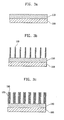
- Light generated in a light emitting diode is mostly confined inside the diode due to total internal reflection with a critical angle at an interface between two media such as a semiconductor and air.
- FIG. 2 is a schematic sectional view showing a light path in a typical light emitting diode.
- a light emitting diode in which an n-semiconductor layer (11), an active layer (12) and a p-semiconductor layer (13) are laminated in sequence on a substrate (10), light (a, b, c) traveling to the outside of the device at an angle less than a critical angle among light emitted from the active layer (12) passes through an interface.
- the light output of the light emitting diode decreases and the characteristics thereof are degraded.
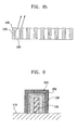
- the active layer (320) and the compound semiconductor layer (330) doped with a second polarity dopant are formed sequentially on the nano rods (310) to form the rod structures (351) spaced apart from one another.
- a planar compound semiconductor layer (370) doped with a second polarity dopant is grown on the compound semiconductor layers (330) doped with a second polarity dopant in the plurality of the rod structures (351).
- the planar compound semiconductor layer (370) is grown at a temperature higher than the growth temperature of the rod structures (351).
- an ohmic-contact and reflective electrode (400) is formed on the planar compound semiconductor layer (370).
Landscapes
- Led Devices (AREA)
- Electrodes Of Semiconductors (AREA)
Applications Claiming Priority (3)
| Application Number | Priority Date | Filing Date | Title |
|---|---|---|---|
| KR1020050043577A KR100658938B1 (ko) | 2005-05-24 | 2005-05-24 | 나노 로드를 갖는 발광 소자 및 그의 제조 방법 |
| KR1020050044373A KR101129094B1 (ko) | 2005-05-26 | 2005-05-26 | 로드형 발광 소자 및 그의 제조방법 |
| EP06290812.4A EP1727216B1 (fr) | 2005-05-24 | 2006-05-18 | Diode électroluminescente à bâtonnets et procédé de fabrication correspondant |
Related Parent Applications (3)
| Application Number | Title | Priority Date | Filing Date |
|---|---|---|---|
| EP06290812.4 Division | 2006-05-18 | ||
| EP06290812.4A Division EP1727216B1 (fr) | 2005-05-24 | 2006-05-18 | Diode électroluminescente à bâtonnets et procédé de fabrication correspondant |
| EP06290812.4A Division-Into EP1727216B1 (fr) | 2005-05-24 | 2006-05-18 | Diode électroluminescente à bâtonnets et procédé de fabrication correspondant |
Publications (3)
| Publication Number | Publication Date |
|---|---|
| EP2410582A2 true EP2410582A2 (fr) | 2012-01-25 |
| EP2410582A3 EP2410582A3 (fr) | 2013-10-23 |
| EP2410582B1 EP2410582B1 (fr) | 2019-09-04 |
Family
ID=36791575
Family Applications (2)
| Application Number | Title | Priority Date | Filing Date |
|---|---|---|---|
| EP06290812.4A Active EP1727216B1 (fr) | 2005-05-24 | 2006-05-18 | Diode électroluminescente à bâtonnets et procédé de fabrication correspondant |
| EP11186011.0A Active EP2410582B1 (fr) | 2005-05-24 | 2006-05-18 | Diode électroluminescente à nano-bâtonnets et procédé de fabrication d'une diode électroluminescente à nano-bâtonnets |
Family Applications Before (1)
| Application Number | Title | Priority Date | Filing Date |
|---|---|---|---|
| EP06290812.4A Active EP1727216B1 (fr) | 2005-05-24 | 2006-05-18 | Diode électroluminescente à bâtonnets et procédé de fabrication correspondant |
Country Status (3)
| Country | Link |
|---|---|
| US (2) | US7947989B2 (fr) |
| EP (2) | EP1727216B1 (fr) |
| JP (1) | JP4740795B2 (fr) |
Cited By (1)
| Publication number | Priority date | Publication date | Assignee | Title |
|---|---|---|---|---|
| US9287445B2 (en) | 2012-12-14 | 2016-03-15 | Samsung Electronics Co., Ltd. | Nano-structured light-emitting devices |
Families Citing this family (85)
| Publication number | Priority date | Publication date | Assignee | Title |
|---|---|---|---|---|
| EP1821347B1 (fr) * | 2006-02-16 | 2018-01-03 | LG Electronics Inc. | Dispositif luminescent de structure verticale et son procédé de fabrication |
| FR2902237B1 (fr) * | 2006-06-09 | 2008-10-10 | Commissariat Energie Atomique | Procede de realisation d'un dispositif microelectronique emetteur de lumiere a nanofils semi-conducteurs formes sur un substrat metallique |
| JP2008066590A (ja) * | 2006-09-08 | 2008-03-21 | Matsushita Electric Works Ltd | 化合物半導体発光素子およびそれを用いる照明装置ならびに化合物半導体素子の製造方法 |
| JP2008098220A (ja) * | 2006-10-06 | 2008-04-24 | Asahi Kasei Corp | 発光ダイオード |
| US8227817B2 (en) | 2006-12-22 | 2012-07-24 | Qunano Ab | Elevated LED |
| US8049203B2 (en) | 2006-12-22 | 2011-11-01 | Qunano Ab | Nanoelectronic structure and method of producing such |
| EP2095426A4 (fr) * | 2006-12-22 | 2012-10-10 | Qunano Ab | Structure nanoélectronique et procédé de production associé |
| WO2008079076A1 (fr) * | 2006-12-22 | 2008-07-03 | Qunano Ab | Diode électroluminescente avec structure de nanofil verticale et procédé de fabrication de celle-ci |
| US8053789B2 (en) | 2006-12-28 | 2011-11-08 | Seoul Opto Device Co., Ltd. | Light emitting device and fabrication method thereof |
| EP2102899B1 (fr) * | 2007-01-12 | 2020-11-11 | QuNano AB | Nanofils de nitrure et leur procede de fabrication |
| WO2008129859A1 (fr) * | 2007-04-13 | 2008-10-30 | Panasonic Corporation | Elément d'émission de lumière et dispositif d'affichage |
| JP5112761B2 (ja) * | 2007-06-26 | 2013-01-09 | パナソニック株式会社 | 化合物半導体素子およびそれを用いる照明装置ならびに化合物半導体素子の製造方法 |
| KR20090012493A (ko) * | 2007-07-30 | 2009-02-04 | 삼성전기주식회사 | 광자결정 발광소자 |
| JP5247109B2 (ja) * | 2007-10-05 | 2013-07-24 | パナソニック株式会社 | 半導体発光装置およびそれを用いる照明装置ならびに半導体発光装置の製造方法 |
| FR2922685B1 (fr) * | 2007-10-22 | 2011-02-25 | Commissariat Energie Atomique | Dispositif optoelectronique a base de nanofils et procedes correspondants |
| KR101541560B1 (ko) | 2007-10-26 | 2015-08-03 | 큐나노 에이비 | 이종 재료상의 나노와이어 성장 |
| KR20090058952A (ko) * | 2007-12-05 | 2009-06-10 | 삼성전자주식회사 | 나노로드를 이용한 발광소자 및 그 제조 방법 |
| JP5097532B2 (ja) * | 2007-12-21 | 2012-12-12 | パナソニック株式会社 | 化合物半導体発光素子の製造方法 |
| JP4856666B2 (ja) * | 2008-03-26 | 2012-01-18 | 独立行政法人科学技術振興機構 | 発光ダイオード素子及びその製造方法 |
| KR101496151B1 (ko) * | 2008-06-25 | 2015-02-27 | 삼성전자주식회사 | 산화물 다이오드를 이용한 디스플레이 장치 |
| KR20110039313A (ko) | 2008-07-07 | 2011-04-15 | 글로 에이비 | 나노구조 led |
| US20110168976A1 (en) * | 2008-07-24 | 2011-07-14 | The Regents Of The University Of California | Micro- and nano-structured led and oled devices |
| KR100956499B1 (ko) * | 2008-08-01 | 2010-05-07 | 주식회사 실트론 | 금속층을 가지는 화합물 반도체 기판, 그 제조 방법 및이를 이용한 화합물 반도체 소자 |
| US20110140072A1 (en) * | 2008-08-21 | 2011-06-16 | Nanocrystal Corporation | Defect-free group iii - nitride nanostructures and devices using pulsed and non-pulsed growth techniques |
| TWI379443B (en) * | 2008-11-28 | 2012-12-11 | Univ Nat Taiwan | A lighting device having high efficiency and a method for fabricating the same |
| KR101061150B1 (ko) | 2009-05-22 | 2011-08-31 | 서울대학교산학협력단 | 발광 디바이스와 이의 제조 방법 |
| JP5094824B2 (ja) * | 2009-10-19 | 2012-12-12 | シャープ株式会社 | 棒状構造発光素子、バックライト、照明装置および表示装置 |
| US8872214B2 (en) | 2009-10-19 | 2014-10-28 | Sharp Kabushiki Kaisha | Rod-like light-emitting device, method of manufacturing rod-like light-emitting device, backlight, illuminating device, and display device |
| JP5014403B2 (ja) * | 2009-11-19 | 2012-08-29 | シャープ株式会社 | 棒状構造発光素子、発光装置、発光装置の製造方法、バックライト、照明装置および表示装置 |
| JP5066164B2 (ja) * | 2009-12-07 | 2012-11-07 | シャープ株式会社 | 半導体素子の製造方法 |
| JP2011119617A (ja) * | 2009-12-07 | 2011-06-16 | Sharp Corp | 棒状構造発光素子の製造方法 |
| EP2546900A4 (fr) | 2010-03-12 | 2016-02-17 | Sharp Kk | Procédé de fabrication de dispositif électroluminescent, dispositif électroluminescent, dispositif d'éclairage, retroéclairage, panneau à cristaux liquides, dispositif d'affichage, procédé de fabrication de dispositif d'affichage, procédé de pilotage de dispositif d'affichage et dispositif d'affichage à cristaux liquides |
| JP2011198697A (ja) * | 2010-03-23 | 2011-10-06 | Sharp Corp | 発光装置、発光装置の製造方法、照明装置およびバックライト |
| DE102010012711A1 (de) * | 2010-03-25 | 2011-09-29 | Osram Opto Semiconductors Gmbh | Strahlungsemittierendes Halbleiterbauelement und Verfahren zur Herstellung eines strahlungsemittierenden Halbleiterbauelements |
| SG186261A1 (en) | 2010-06-18 | 2013-01-30 | Glo Ab | Nanowire led structure and method for manufacturing the same |
| KR20150098246A (ko) | 2010-09-01 | 2015-08-27 | 샤프 가부시키가이샤 | 발광 소자 및 그 제조 방법, 발광 장치의 제조 방법, 조명 장치, 백라이트, 표시 장치 및 다이오드 |
| JP4927223B2 (ja) * | 2010-09-01 | 2012-05-09 | シャープ株式会社 | 発光素子およびその製造方法、発光装置の製造方法、照明装置、バックライト並びに表示装置 |
| FR2975532B1 (fr) * | 2011-05-18 | 2013-05-10 | Commissariat Energie Atomique | Connexion electrique en serie de nanofils emetteurs de lumiere |
| KR101217209B1 (ko) * | 2010-10-07 | 2012-12-31 | 서울대학교산학협력단 | 발광소자 및 그 제조방법 |
| TWI573288B (zh) * | 2010-10-18 | 2017-03-01 | 鴻海精密工業股份有限公司 | 發光二極體及其製作方法 |
| CN102456786B (zh) * | 2010-10-29 | 2016-03-09 | 鸿富锦精密工业(深圳)有限公司 | 发光二极管及其制作方法 |
| DE102010051286A1 (de) | 2010-11-12 | 2012-05-16 | Osram Opto Semiconductors Gmbh | Optoelektronischer Halbleiterchip und Verfahren zu dessen Herstellung |
| TWI495155B (zh) * | 2010-12-02 | 2015-08-01 | Epistar Corp | 光電元件及其製造方法 |
| TWI419367B (zh) | 2010-12-02 | 2013-12-11 | Epistar Corp | 光電元件及其製造方法 |
| GB201021112D0 (en) | 2010-12-13 | 2011-01-26 | Ntnu Technology Transfer As | Nanowires |
| US20120146069A1 (en) * | 2010-12-14 | 2012-06-14 | International Business Machines Corporation | Oxide Based LED BEOL Integration |
| KR101209449B1 (ko) * | 2011-04-29 | 2012-12-07 | 피에스아이 주식회사 | 풀-칼라 led 디스플레이 장치 및 그 제조방법 |
| CN102185070A (zh) * | 2011-05-06 | 2011-09-14 | 西安神光安瑞光电科技有限公司 | 发光二极管及其制备方法 |
| CN102185068A (zh) * | 2011-05-06 | 2011-09-14 | 西安神光安瑞光电科技有限公司 | 发光二极管及其制备方法 |
| US8604491B2 (en) * | 2011-07-21 | 2013-12-10 | Tsmc Solid State Lighting Ltd. | Wafer level photonic device die structure and method of making the same |
| DE102011112706B4 (de) * | 2011-09-07 | 2021-09-02 | OSRAM Opto Semiconductors Gesellschaft mit beschränkter Haftung | Optoelektronisches Bauelement |
| US8350249B1 (en) * | 2011-09-26 | 2013-01-08 | Glo Ab | Coalesced nanowire structures with interstitial voids and method for manufacturing the same |
| DE102011056140A1 (de) * | 2011-12-07 | 2013-06-13 | Osram Opto Semiconductors Gmbh | Optoelektronischer Halbleiterchip |
| FR2984599B1 (fr) * | 2011-12-20 | 2014-01-17 | Commissariat Energie Atomique | Procede de fabrication d'un micro- ou nano- fil semiconducteur, structure semiconductrice comportant un tel micro- ou nano- fil et procede de fabrication d'une structure semiconductrice |
| WO2013121289A2 (fr) | 2012-02-14 | 2013-08-22 | Qunano Ab | Electronique à base de nanofil de nitrure de gallium |
| DE102012101718B4 (de) * | 2012-03-01 | 2025-08-28 | OSRAM Opto Semiconductors Gesellschaft mit beschränkter Haftung | Optoelektronischer Halbleiterchip |
| GB201211038D0 (en) | 2012-06-21 | 2012-08-01 | Norwegian Univ Sci & Tech Ntnu | Solar cells |
| FR3000294B1 (fr) * | 2012-12-21 | 2016-03-04 | Aledia | Support fonctionnel comprenant des nanofils et des nano-empreintes et procede de fabrication dudit support |
| KR101603207B1 (ko) | 2013-01-29 | 2016-03-14 | 삼성전자주식회사 | 나노구조 반도체 발광소자 제조방법 |
| US11502219B2 (en) * | 2013-03-14 | 2022-11-15 | The Royal Institution For The Advancement Of Learning/Mcgill University | Methods and devices for solid state nanowire devices |
| FR3004006B1 (fr) * | 2013-03-28 | 2016-10-07 | Aledia | Dispositif electroluminescent a nanofils actifs et nanofils de contact et procede de fabrication |
| FR3004000B1 (fr) * | 2013-03-28 | 2016-07-15 | Aledia | Dispositif electroluminescent avec capteur integre et procede de controle de l'emission du dispositif |
| GB201311101D0 (en) | 2013-06-21 | 2013-08-07 | Norwegian Univ Sci & Tech Ntnu | Semiconducting Films |
| FR3011383B1 (fr) * | 2013-09-30 | 2017-05-26 | Commissariat Energie Atomique | Procede de fabrication de dispositifs optoelectroniques a diodes electroluminescentes |
| US9099573B2 (en) | 2013-10-31 | 2015-08-04 | Samsung Electronics Co., Ltd. | Nano-structure semiconductor light emitting device |
| KR102285786B1 (ko) * | 2014-01-20 | 2021-08-04 | 삼성전자 주식회사 | 반도체 발광 소자 |
| WO2016022824A1 (fr) | 2014-08-08 | 2016-02-11 | Glo Ab | Dispositif d'affichage pixélisé basé sur des led à nanofils et son procédé de fabrication |
| KR102227771B1 (ko) | 2014-08-25 | 2021-03-16 | 삼성전자주식회사 | 나노구조 반도체 발광소자 |
| WO2016049507A1 (fr) | 2014-09-26 | 2016-03-31 | Glo Ab | Puce d'image monolithique pour affichage proche de l'œil |
| EA201890168A1 (ru) | 2015-07-13 | 2018-08-31 | Крайонано Ас | Нанопроволока или нанопирамидки, выращенные на графитовой подложке |
| TWI772266B (zh) | 2015-07-13 | 2022-08-01 | 挪威商卡亞奈米公司 | 發光二極體裝置及光偵測器裝置 |
| CA2993884A1 (fr) | 2015-07-31 | 2017-02-09 | Crayonano As | Procedes de croissance de nanofils ou de nanopyramides sur des substrats graphitiques |
| US10374127B2 (en) * | 2015-09-17 | 2019-08-06 | Nxp Usa, Inc. | Electronic devices with nanorings, and methods of manufacture thereof |
| JP6149247B1 (ja) * | 2016-11-21 | 2017-06-21 | 株式会社奥本研究所 | 発光デバイスおよびその製造方法 |
| KR102707509B1 (ko) | 2016-12-19 | 2024-09-23 | 삼성디스플레이 주식회사 | 발광장치 및 그의 제조방법 |
| KR102587958B1 (ko) * | 2017-02-03 | 2023-10-11 | 삼성전자주식회사 | 메타 광학 소자 및 그 제조 방법 |
| FR3063129B1 (fr) * | 2017-02-17 | 2019-04-12 | Valeo Vision | Module lumineux a encombrement reduit |
| GB201705755D0 (en) * | 2017-04-10 | 2017-05-24 | Norwegian Univ Of Science And Tech (Ntnu) | Nanostructure |
| US11063178B2 (en) | 2017-10-25 | 2021-07-13 | Sensor Electronic Technology, Inc. | Semiconductor heterostructure with improved light emission |
| CN108565322A (zh) * | 2018-06-01 | 2018-09-21 | 广东工业大学 | 一种led外延芯片及一种led外延芯片的制备方法 |
| FR3083002B1 (fr) * | 2018-06-20 | 2020-07-31 | Aledia | Dispositif optoelectronique comprenant une matrice de diodes |
| GB2575311B (en) * | 2018-07-06 | 2021-03-03 | Plessey Semiconductors Ltd | Monolithic LED array and a precursor thereto |
| GB201913701D0 (en) | 2019-09-23 | 2019-11-06 | Crayonano As | Composition of matter |
| KR20220152284A (ko) * | 2020-03-11 | 2022-11-15 | 루미레즈 엘엘씨 | 금속 그리드를 포함하는 레이저 리프트-오프 처리 시스템 |
| JP7826742B2 (ja) | 2022-03-04 | 2026-03-10 | セイコーエプソン株式会社 | 発光装置、プロジェクター、およびディスプレイ |
Family Cites Families (46)
| Publication number | Priority date | Publication date | Assignee | Title |
|---|---|---|---|---|
| US4920793A (en) * | 1986-05-23 | 1990-05-01 | Djorup Robert Sonny | Directional thermal anemometer transducer |
| JPH06244457A (ja) * | 1993-02-16 | 1994-09-02 | Nisshin Steel Co Ltd | 発光ダイオードの製造方法 |
| CN1082254C (zh) * | 1995-08-22 | 2002-04-03 | 松下电器产业株式会社 | 硅结构体及其制造方法和装置及使用硅结构体的太阳电池 |
| JP3517091B2 (ja) * | 1997-07-04 | 2004-04-05 | 東芝電子エンジニアリング株式会社 | 窒化ガリウム系半導体発光素子およびその製造方法 |
| JP4083866B2 (ja) * | 1998-04-28 | 2008-04-30 | シャープ株式会社 | 半導体レーザ素子 |
| JP2000208874A (ja) * | 1999-01-12 | 2000-07-28 | Sony Corp | 窒化物半導体と、窒化物半導体発光装置と、窒化物半導体の製造方法と、半導体発光装置の製造方法 |
| US6992334B1 (en) * | 1999-12-22 | 2006-01-31 | Lumileds Lighting U.S., Llc | Multi-layer highly reflective ohmic contacts for semiconductor devices |
| JP3662806B2 (ja) * | 2000-03-29 | 2005-06-22 | 日本電気株式会社 | 窒化物系半導体層の製造方法 |
| JP3882539B2 (ja) * | 2000-07-18 | 2007-02-21 | ソニー株式会社 | 半導体発光素子およびその製造方法、並びに画像表示装置 |
| US20020017652A1 (en) * | 2000-08-08 | 2002-02-14 | Stefan Illek | Semiconductor chip for optoelectronics |
| JP4672839B2 (ja) * | 2000-09-06 | 2011-04-20 | キヤノン株式会社 | 発光体、構造体及びその製造方法 |
| JP4595198B2 (ja) * | 2000-12-15 | 2010-12-08 | ソニー株式会社 | 半導体発光素子及び半導体発光素子の製造方法 |
| JP3946969B2 (ja) * | 2001-05-31 | 2007-07-18 | 日本碍子株式会社 | 電界効果トランジスタ、及びヘテロ接合型バイポーラトランジスタ |
| EP1422748A1 (fr) * | 2001-08-01 | 2004-05-26 | Nagoya Industrial Science Research Institute | Film semi-conducteur en nitrure du groupe iii et son procede de production |
| JP4254157B2 (ja) * | 2001-08-22 | 2009-04-15 | ソニー株式会社 | 窒化物半導体素子及び窒化物半導体素子の製造方法 |
| US6818465B2 (en) * | 2001-08-22 | 2004-11-16 | Sony Corporation | Nitride semiconductor element and production method for nitride semiconductor element |
| JP2003101069A (ja) * | 2001-09-25 | 2003-04-04 | Nagoya Industrial Science Research Inst | Iii族窒化物量子ドットおよびその製造方法 |
| US6963086B2 (en) * | 2001-10-10 | 2005-11-08 | Sony Corporation | Semiconductor light-emitting device image display illuminator and its manufacturing method |
| TWI220319B (en) * | 2002-03-11 | 2004-08-11 | Solidlite Corp | Nano-wire light emitting device |
| JP4514402B2 (ja) * | 2002-10-28 | 2010-07-28 | シャープ株式会社 | 半導体素子及びその製造方法 |
| KR101089123B1 (ko) * | 2002-11-05 | 2011-12-05 | 코닌클리케 필립스 일렉트로닉스 엔.브이. | 무기 반도체 물질의 나노구조물, 전자 디바이스, 화합물 반도체 물질의 나노구조물 제조 방법, 및 전자 디바이스 제조 방법 |
| US6969897B2 (en) * | 2002-12-10 | 2005-11-29 | Kim Ii John | Optoelectronic devices employing fibers for light collection and emission |
| JP2004288799A (ja) * | 2003-03-20 | 2004-10-14 | Sony Corp | 半導体発光素子およびその製造方法、集積型半導体発光装置およびその製造方法、画像表示装置およびその製造方法ならびに照明装置およびその製造方法 |
| US20040252737A1 (en) * | 2003-06-16 | 2004-12-16 | Gyu Chul Yi | Zinc oxide based nanorod with quantum well or coaxial quantum structure |
| KR100593264B1 (ko) * | 2003-06-26 | 2006-06-26 | 학교법인 포항공과대학교 | p-타입 반도체 박막과 n-타입 산화아연(ZnO)계나노막대의 이종접합 구조체, 이의 제법 및 이를 이용한소자 |
| US20050040212A1 (en) * | 2003-08-23 | 2005-02-24 | Kuang-Neng Yang | Method for manufacturing nitride light-emitting device |
| KR100644166B1 (ko) * | 2004-02-12 | 2006-11-10 | 학교법인 포항공과대학교 | 질화물 반도체의 이종접합 구조체, 이를 포함하는나노소자 또는 이의 어레이 |
| JP4160000B2 (ja) * | 2004-02-13 | 2008-10-01 | ドンゴク ユニバーシティ インダストリー アカデミック コーポレイション ファウンデイション | 発光ダイオードおよびその製造方法 |
| KR100646696B1 (ko) * | 2004-03-10 | 2006-11-23 | 주식회사 실트론 | 질화물 반도체 소자 및 그 제조방법 |
| KR100624419B1 (ko) * | 2004-04-07 | 2006-09-19 | 삼성전자주식회사 | 나노와이어 발광소자 및 그 제조방법 |
| KR100553317B1 (ko) * | 2004-04-23 | 2006-02-20 | 한국과학기술연구원 | 실리콘 나노선을 이용한 실리콘 광소자 및 이의 제조방법 |
| KR100616600B1 (ko) * | 2004-08-24 | 2006-08-28 | 삼성전기주식회사 | 수직구조 질화물 반도체 발광소자 |
| KR100664986B1 (ko) * | 2004-10-29 | 2007-01-09 | 삼성전기주식회사 | 나노로드를 이용한 질화물계 반도체 소자 및 그 제조 방법 |
| US7180097B2 (en) * | 2004-11-12 | 2007-02-20 | Formosa Epitaxy Incorporation | High-brightness gallium-nitride based light emitting diode structure |
| US7202173B2 (en) * | 2004-12-20 | 2007-04-10 | Palo Alto Research Corporation Incorporated | Systems and methods for electrical contacts to arrays of vertically aligned nanorods |
| US20060207647A1 (en) * | 2005-03-16 | 2006-09-21 | General Electric Company | High efficiency inorganic nanorod-enhanced photovoltaic devices |
| CN1850580A (zh) * | 2005-04-22 | 2006-10-25 | 清华大学 | 超晶格纳米器件及其制作方法 |
| WO2007001098A1 (fr) * | 2005-06-25 | 2007-01-04 | Seoul Opto Device Co., Ltd. | Nanostructure comprenant un puits quantique à base de nitrure et diode électroluminescente l'utilisant |
| KR20070021671A (ko) * | 2005-08-19 | 2007-02-23 | 서울옵토디바이스주식회사 | 나노막대들의 어레이를 채택한 발광 다이오드 및 그것을제조하는 방법 |
| US7635600B2 (en) * | 2005-11-16 | 2009-12-22 | Sharp Laboratories Of America, Inc. | Photovoltaic structure with a conductive nanowire array electrode |
| AU2007313096B2 (en) * | 2006-03-10 | 2011-11-10 | Unm Rainforest Innovations | Pulsed growth of GaN nanowires and applications in group III nitride semiconductor substrate materials and devices |
| US8227817B2 (en) * | 2006-12-22 | 2012-07-24 | Qunano Ab | Elevated LED |
| TWI411124B (zh) * | 2007-07-10 | 2013-10-01 | Delta Electronics Inc | 發光二極體裝置及其製造方法 |
| KR20090058952A (ko) * | 2007-12-05 | 2009-06-10 | 삼성전자주식회사 | 나노로드를 이용한 발광소자 및 그 제조 방법 |
| TWI389346B (zh) * | 2008-10-01 | 2013-03-11 | Epistar Corp | 光電元件 |
| TWI396307B (zh) * | 2009-02-05 | 2013-05-11 | Huga Optotech Inc | 發光二極體 |
-
2006
- 2006-05-18 EP EP06290812.4A patent/EP1727216B1/fr active Active
- 2006-05-18 EP EP11186011.0A patent/EP2410582B1/fr active Active
- 2006-05-18 JP JP2006139266A patent/JP4740795B2/ja active Active
- 2006-05-19 US US11/436,771 patent/US7947989B2/en active Active
-
2011
- 2011-04-15 US US13/088,139 patent/US8653538B2/en active Active
Non-Patent Citations (1)
| Title |
|---|
| None |
Cited By (2)
| Publication number | Priority date | Publication date | Assignee | Title |
|---|---|---|---|---|
| US9287445B2 (en) | 2012-12-14 | 2016-03-15 | Samsung Electronics Co., Ltd. | Nano-structured light-emitting devices |
| US9525100B2 (en) | 2012-12-14 | 2016-12-20 | Samsung Electronics Co., Ltd. | Nano-structured light-emitting devices |
Also Published As
| Publication number | Publication date |
|---|---|
| JP4740795B2 (ja) | 2011-08-03 |
| JP2006332650A (ja) | 2006-12-07 |
| US7947989B2 (en) | 2011-05-24 |
| EP2410582B1 (fr) | 2019-09-04 |
| EP2410582A3 (fr) | 2013-10-23 |
| US8653538B2 (en) | 2014-02-18 |
| EP1727216A3 (fr) | 2011-07-27 |
| US20070041214A1 (en) | 2007-02-22 |
| EP1727216A2 (fr) | 2006-11-29 |
| US20110272723A1 (en) | 2011-11-10 |
| EP1727216B1 (fr) | 2019-04-24 |
Similar Documents
| Publication | Publication Date | Title |
|---|---|---|
| EP1727216B1 (fr) | Diode électroluminescente à bâtonnets et procédé de fabrication correspondant | |
| US7893448B2 (en) | Light emitting device having nano structures for light extraction | |
| US7763881B2 (en) | Photonic crystal light emitting device | |
| JP4927042B2 (ja) | 光子結晶発光素子及びその製造方法 | |
| US8546819B2 (en) | Light emitting device and fabrication method thereof | |
| US8592842B2 (en) | Vertical light emitting diodes | |
| JP5237274B2 (ja) | 発光素子及び照明装置 | |
| JP5045418B2 (ja) | GaN系LED素子、GaN系LED素子の製造方法およびGaN系LED素子製造用テンプレート | |
| WO2002075821A1 (fr) | Dispositif luminescent semiconducteur | |
| TW200423421A (en) | Improved LED efficiency using photonic crystal structure | |
| KR20080087175A (ko) | 반도체 발광 소자 | |
| CN102810609A (zh) | 一种紫外半导体发光器件及其制造方法 | |
| WO2011129858A1 (fr) | Dispositifs électroluminescents avec mécanisme d'extraction verticale de la lumière, ainsi que procédé de fabrication de ceux-ci | |
| KR102602285B1 (ko) | 나노막대를 포함하는 나노막대 발광 구조물, 발광소자 및 그 제조방법, 그의 패키지 및 이를 포함하는 조명장치 | |
| JP5038382B2 (ja) | 半導体発光素子 | |
| KR20120055391A (ko) | 나노로드 발광소자 | |
| US8664020B2 (en) | Semiconductor light emitting device and method of manufacturing the same | |
| KR20080093556A (ko) | 질화물계 발광 소자 및 그 제조방법 | |
| JP2012080104A (ja) | 半導体発光素子及びその製造方法 | |
| KR20110103686A (ko) | 질화물 반도체 발광소자 및 그 제조방법 | |
| CN107591463B (zh) | 发光组件及发光组件的制造方法 | |
| JP2011082248A (ja) | 半導体発光素子及びその製造方法、並びにランプ | |
| JP2008053385A (ja) | 窒化物半導体発光ダイオード素子 | |
| JP2008047850A (ja) | 窒化物半導体発光ダイオード素子 | |
| KR20110091246A (ko) | 반도체 발광소자의 제조방법 및 이에 의해 제조된 반도체 발광소자 |
Legal Events
| Date | Code | Title | Description |
|---|---|---|---|
| AC | Divisional application: reference to earlier application |
Ref document number: 1727216 Country of ref document: EP Kind code of ref document: P |
|
| AK | Designated contracting states |
Kind code of ref document: A2 Designated state(s): AT BE BG CH CY CZ DE DK EE ES FI FR GB GR HU IE IS IT LI LT LU LV MC NL PL PT RO SE SI SK TR |
|
| PUAI | Public reference made under article 153(3) epc to a published international application that has entered the european phase |
Free format text: ORIGINAL CODE: 0009012 |
|
| PUAL | Search report despatched |
Free format text: ORIGINAL CODE: 0009013 |
|
| AK | Designated contracting states |
Kind code of ref document: A3 Designated state(s): AT BE BG CH CY CZ DE DK EE ES FI FR GB GR HU IE IS IT LI LT LU LV MC NL PL PT RO SE SI SK TR |
|
| RIC1 | Information provided on ipc code assigned before grant |
Ipc: H01L 33/00 20100101AFI20130918BHEP Ipc: H01L 33/32 20100101ALN20130918BHEP Ipc: B82Y 20/00 20110101ALN20130918BHEP Ipc: H01L 33/08 20100101ALN20130918BHEP Ipc: H01L 33/18 20100101ALI20130918BHEP Ipc: H01L 33/28 20100101ALN20130918BHEP |
|
| 17P | Request for examination filed |
Effective date: 20140331 |
|
| RBV | Designated contracting states (corrected) |
Designated state(s): AT BE BG CH CY CZ DE DK EE ES FI FR GB GR HU IE IS IT LI LT LU LV MC NL PL PT RO SE SI SK TR |
|
| RAP1 | Party data changed (applicant data changed or rights of an application transferred) |
Owner name: LG INNOTEK CO., LTD. Owner name: LG ELECTRONICS INC. |
|
| RAP1 | Party data changed (applicant data changed or rights of an application transferred) |
Owner name: LG INNOTEK CO., LTD. Owner name: LG ELECTRONICS INC. |
|
| REG | Reference to a national code |
Ref country code: DE Ref legal event code: R079 Ref document number: 602006058561 Country of ref document: DE Free format text: PREVIOUS MAIN CLASS: H01L0033080000 Ipc: H01L0033180000 |
|
| GRAP | Despatch of communication of intention to grant a patent |
Free format text: ORIGINAL CODE: EPIDOSNIGR1 |
|
| STAA | Information on the status of an ep patent application or granted ep patent |
Free format text: STATUS: GRANT OF PATENT IS INTENDED |
|
| RIC1 | Information provided on ipc code assigned before grant |
Ipc: H01L 33/28 20100101ALN20190220BHEP Ipc: H01L 33/18 20100101AFI20190220BHEP Ipc: H01L 33/42 20100101ALN20190220BHEP Ipc: H01L 33/08 20100101ALN20190220BHEP Ipc: H01L 33/32 20100101ALN20190220BHEP Ipc: B82Y 20/00 20110101ALN20190220BHEP Ipc: H01L 33/00 20100101ALI20190220BHEP Ipc: H01L 33/40 20100101ALN20190220BHEP |
|
| INTG | Intention to grant announced |
Effective date: 20190319 |
|
| GRAS | Grant fee paid |
Free format text: ORIGINAL CODE: EPIDOSNIGR3 |
|
| GRAA | (expected) grant |
Free format text: ORIGINAL CODE: 0009210 |
|
| STAA | Information on the status of an ep patent application or granted ep patent |
Free format text: STATUS: THE PATENT HAS BEEN GRANTED |
|
| RAP1 | Party data changed (applicant data changed or rights of an application transferred) |
Owner name: LG ELECTRONICS INC. Owner name: LG INNOTEK CO., LTD. |
|
| AC | Divisional application: reference to earlier application |
Ref document number: 1727216 Country of ref document: EP Kind code of ref document: P |
|
| AK | Designated contracting states |
Kind code of ref document: B1 Designated state(s): AT BE BG CH CY CZ DE DK EE ES FI FR GB GR HU IE IS IT LI LT LU LV MC NL PL PT RO SE SI SK TR |
|
| REG | Reference to a national code |
Ref country code: GB Ref legal event code: FG4D |
|
| REG | Reference to a national code |
Ref country code: CH Ref legal event code: EP |
|
| REG | Reference to a national code |
Ref country code: AT Ref legal event code: REF Ref document number: 1176598 Country of ref document: AT Kind code of ref document: T Effective date: 20190915 |
|
| REG | Reference to a national code |
Ref country code: DE Ref legal event code: R096 Ref document number: 602006058561 Country of ref document: DE |
|
| REG | Reference to a national code |
Ref country code: IE Ref legal event code: FG4D |
|
| REG | Reference to a national code |
Ref country code: NL Ref legal event code: MP Effective date: 20190904 |
|
| REG | Reference to a national code |
Ref country code: LT Ref legal event code: MG4D |
|
| PG25 | Lapsed in a contracting state [announced via postgrant information from national office to epo] |
Ref country code: SE Free format text: LAPSE BECAUSE OF FAILURE TO SUBMIT A TRANSLATION OF THE DESCRIPTION OR TO PAY THE FEE WITHIN THE PRESCRIBED TIME-LIMIT Effective date: 20190904 Ref country code: LT Free format text: LAPSE BECAUSE OF FAILURE TO SUBMIT A TRANSLATION OF THE DESCRIPTION OR TO PAY THE FEE WITHIN THE PRESCRIBED TIME-LIMIT Effective date: 20190904 Ref country code: BG Free format text: LAPSE BECAUSE OF FAILURE TO SUBMIT A TRANSLATION OF THE DESCRIPTION OR TO PAY THE FEE WITHIN THE PRESCRIBED TIME-LIMIT Effective date: 20191204 Ref country code: FI Free format text: LAPSE BECAUSE OF FAILURE TO SUBMIT A TRANSLATION OF THE DESCRIPTION OR TO PAY THE FEE WITHIN THE PRESCRIBED TIME-LIMIT Effective date: 20190904 |
|
| PG25 | Lapsed in a contracting state [announced via postgrant information from national office to epo] |
Ref country code: GR Free format text: LAPSE BECAUSE OF FAILURE TO SUBMIT A TRANSLATION OF THE DESCRIPTION OR TO PAY THE FEE WITHIN THE PRESCRIBED TIME-LIMIT Effective date: 20191205 Ref country code: ES Free format text: LAPSE BECAUSE OF FAILURE TO SUBMIT A TRANSLATION OF THE DESCRIPTION OR TO PAY THE FEE WITHIN THE PRESCRIBED TIME-LIMIT Effective date: 20190904 Ref country code: LV Free format text: LAPSE BECAUSE OF FAILURE TO SUBMIT A TRANSLATION OF THE DESCRIPTION OR TO PAY THE FEE WITHIN THE PRESCRIBED TIME-LIMIT Effective date: 20190904 |
|
| REG | Reference to a national code |
Ref country code: AT Ref legal event code: MK05 Ref document number: 1176598 Country of ref document: AT Kind code of ref document: T Effective date: 20190904 |
|
| PG25 | Lapsed in a contracting state [announced via postgrant information from national office to epo] |
Ref country code: NL Free format text: LAPSE BECAUSE OF FAILURE TO SUBMIT A TRANSLATION OF THE DESCRIPTION OR TO PAY THE FEE WITHIN THE PRESCRIBED TIME-LIMIT Effective date: 20190904 Ref country code: EE Free format text: LAPSE BECAUSE OF FAILURE TO SUBMIT A TRANSLATION OF THE DESCRIPTION OR TO PAY THE FEE WITHIN THE PRESCRIBED TIME-LIMIT Effective date: 20190904 Ref country code: AT Free format text: LAPSE BECAUSE OF FAILURE TO SUBMIT A TRANSLATION OF THE DESCRIPTION OR TO PAY THE FEE WITHIN THE PRESCRIBED TIME-LIMIT Effective date: 20190904 Ref country code: IT Free format text: LAPSE BECAUSE OF FAILURE TO SUBMIT A TRANSLATION OF THE DESCRIPTION OR TO PAY THE FEE WITHIN THE PRESCRIBED TIME-LIMIT Effective date: 20190904 Ref country code: RO Free format text: LAPSE BECAUSE OF FAILURE TO SUBMIT A TRANSLATION OF THE DESCRIPTION OR TO PAY THE FEE WITHIN THE PRESCRIBED TIME-LIMIT Effective date: 20190904 Ref country code: PT Free format text: LAPSE BECAUSE OF FAILURE TO SUBMIT A TRANSLATION OF THE DESCRIPTION OR TO PAY THE FEE WITHIN THE PRESCRIBED TIME-LIMIT Effective date: 20200106 Ref country code: PL Free format text: LAPSE BECAUSE OF FAILURE TO SUBMIT A TRANSLATION OF THE DESCRIPTION OR TO PAY THE FEE WITHIN THE PRESCRIBED TIME-LIMIT Effective date: 20190904 |
|
| PG25 | Lapsed in a contracting state [announced via postgrant information from national office to epo] |
Ref country code: IS Free format text: LAPSE BECAUSE OF FAILURE TO SUBMIT A TRANSLATION OF THE DESCRIPTION OR TO PAY THE FEE WITHIN THE PRESCRIBED TIME-LIMIT Effective date: 20200224 Ref country code: SK Free format text: LAPSE BECAUSE OF FAILURE TO SUBMIT A TRANSLATION OF THE DESCRIPTION OR TO PAY THE FEE WITHIN THE PRESCRIBED TIME-LIMIT Effective date: 20190904 Ref country code: CZ Free format text: LAPSE BECAUSE OF FAILURE TO SUBMIT A TRANSLATION OF THE DESCRIPTION OR TO PAY THE FEE WITHIN THE PRESCRIBED TIME-LIMIT Effective date: 20190904 |
|
| REG | Reference to a national code |
Ref country code: DE Ref legal event code: R097 Ref document number: 602006058561 Country of ref document: DE |
|
| PLBE | No opposition filed within time limit |
Free format text: ORIGINAL CODE: 0009261 |
|
| STAA | Information on the status of an ep patent application or granted ep patent |
Free format text: STATUS: NO OPPOSITION FILED WITHIN TIME LIMIT |
|
| PG2D | Information on lapse in contracting state deleted |
Ref country code: IS |
|
| PG25 | Lapsed in a contracting state [announced via postgrant information from national office to epo] |
Ref country code: DK Free format text: LAPSE BECAUSE OF FAILURE TO SUBMIT A TRANSLATION OF THE DESCRIPTION OR TO PAY THE FEE WITHIN THE PRESCRIBED TIME-LIMIT Effective date: 20190904 Ref country code: IS Free format text: LAPSE BECAUSE OF FAILURE TO SUBMIT A TRANSLATION OF THE DESCRIPTION OR TO PAY THE FEE WITHIN THE PRESCRIBED TIME-LIMIT Effective date: 20200105 |
|
| 26N | No opposition filed |
Effective date: 20200605 |
|
| PG25 | Lapsed in a contracting state [announced via postgrant information from national office to epo] |
Ref country code: SI Free format text: LAPSE BECAUSE OF FAILURE TO SUBMIT A TRANSLATION OF THE DESCRIPTION OR TO PAY THE FEE WITHIN THE PRESCRIBED TIME-LIMIT Effective date: 20190904 |
|
| PG25 | Lapsed in a contracting state [announced via postgrant information from national office to epo] |
Ref country code: LI Free format text: LAPSE BECAUSE OF NON-PAYMENT OF DUE FEES Effective date: 20200531 Ref country code: MC Free format text: LAPSE BECAUSE OF FAILURE TO SUBMIT A TRANSLATION OF THE DESCRIPTION OR TO PAY THE FEE WITHIN THE PRESCRIBED TIME-LIMIT Effective date: 20190904 Ref country code: CH Free format text: LAPSE BECAUSE OF NON-PAYMENT OF DUE FEES Effective date: 20200531 |
|
| REG | Reference to a national code |
Ref country code: BE Ref legal event code: MM Effective date: 20200531 |
|
| GBPC | Gb: european patent ceased through non-payment of renewal fee |
Effective date: 20200518 |
|
| PG25 | Lapsed in a contracting state [announced via postgrant information from national office to epo] |
Ref country code: LU Free format text: LAPSE BECAUSE OF NON-PAYMENT OF DUE FEES Effective date: 20200518 |
|
| PG25 | Lapsed in a contracting state [announced via postgrant information from national office to epo] |
Ref country code: IE Free format text: LAPSE BECAUSE OF NON-PAYMENT OF DUE FEES Effective date: 20200518 Ref country code: FR Free format text: LAPSE BECAUSE OF NON-PAYMENT OF DUE FEES Effective date: 20200531 Ref country code: GB Free format text: LAPSE BECAUSE OF NON-PAYMENT OF DUE FEES Effective date: 20200518 |
|
| PG25 | Lapsed in a contracting state [announced via postgrant information from national office to epo] |
Ref country code: BE Free format text: LAPSE BECAUSE OF NON-PAYMENT OF DUE FEES Effective date: 20200531 |
|
| REG | Reference to a national code |
Ref country code: DE Ref legal event code: R081 Ref document number: 602006058561 Country of ref document: DE Owner name: LG INNOTEK CO., LTD., KR Free format text: FORMER OWNERS: LG ELECTRONICS INC., SEOUL, KR; LG INNOTEK CO., LTD., SEOUL, KR Ref country code: DE Ref legal event code: R081 Ref document number: 602006058561 Country of ref document: DE Owner name: SUZHOU LEKIN SEMICONDUCTOR CO. LTD., TAICANG, CN Free format text: FORMER OWNERS: LG ELECTRONICS INC., SEOUL, KR; LG INNOTEK CO., LTD., SEOUL, KR Ref country code: DE Ref legal event code: R081 Ref document number: 602006058561 Country of ref document: DE Owner name: LG ELECTRONICS INC., KR Free format text: FORMER OWNERS: LG ELECTRONICS INC., SEOUL, KR; LG INNOTEK CO., LTD., SEOUL, KR |
|
| PG25 | Lapsed in a contracting state [announced via postgrant information from national office to epo] |
Ref country code: TR Free format text: LAPSE BECAUSE OF FAILURE TO SUBMIT A TRANSLATION OF THE DESCRIPTION OR TO PAY THE FEE WITHIN THE PRESCRIBED TIME-LIMIT Effective date: 20190904 Ref country code: CY Free format text: LAPSE BECAUSE OF FAILURE TO SUBMIT A TRANSLATION OF THE DESCRIPTION OR TO PAY THE FEE WITHIN THE PRESCRIBED TIME-LIMIT Effective date: 20190904 |
|
| REG | Reference to a national code |
Ref country code: DE Ref legal event code: R081 Ref document number: 602006058561 Country of ref document: DE Owner name: LG INNOTEK CO., LTD., KR Free format text: FORMER OWNERS: LG ELECTRONICS INC., SEOUL, KR; SUZHOU LEKIN SEMICONDUCTOR CO. LTD., TAICANG, SUZHOU, CN Ref country code: DE Ref legal event code: R081 Ref document number: 602006058561 Country of ref document: DE Owner name: LG ELECTRONICS INC., KR Free format text: FORMER OWNERS: LG ELECTRONICS INC., SEOUL, KR; SUZHOU LEKIN SEMICONDUCTOR CO. LTD., TAICANG, SUZHOU, CN |
|
| REG | Reference to a national code |
Ref country code: DE Ref legal event code: R079 Ref document number: 602006058561 Country of ref document: DE Free format text: PREVIOUS MAIN CLASS: H01L0033180000 Ipc: H10H0020818000 |
|
| PGFP | Annual fee paid to national office [announced via postgrant information from national office to epo] |
Ref country code: DE Payment date: 20250422 Year of fee payment: 20 |