EP2431120A1 - Method of forming periodic structures in thin films using interfering laser beams - Google Patents
Method of forming periodic structures in thin films using interfering laser beams Download PDFInfo
- Publication number
- EP2431120A1 EP2431120A1 EP11160615A EP11160615A EP2431120A1 EP 2431120 A1 EP2431120 A1 EP 2431120A1 EP 11160615 A EP11160615 A EP 11160615A EP 11160615 A EP11160615 A EP 11160615A EP 2431120 A1 EP2431120 A1 EP 2431120A1
- Authority
- EP
- European Patent Office
- Prior art keywords
- film
- intensity
- beams
- interfering
- interference
- Prior art date
- Legal status (The legal status is an assumption and is not a legal conclusion. Google has not performed a legal analysis and makes no representation as to the accuracy of the status listed.)
- Granted
Links
Images


Classifications
-
- B—PERFORMING OPERATIONS; TRANSPORTING
- B82—NANOTECHNOLOGY
- B82Y—SPECIFIC USES OR APPLICATIONS OF NANOSTRUCTURES; MEASUREMENT OR ANALYSIS OF NANOSTRUCTURES; MANUFACTURE OR TREATMENT OF NANOSTRUCTURES
- B82Y40/00—Manufacture or treatment of nanostructures
-
- B—PERFORMING OPERATIONS; TRANSPORTING
- B23—MACHINE TOOLS; METAL-WORKING NOT OTHERWISE PROVIDED FOR
- B23K—SOLDERING OR UNSOLDERING; WELDING; CLADDING OR PLATING BY SOLDERING OR WELDING; CUTTING BY APPLYING HEAT LOCALLY, e.g. FLAME CUTTING; WORKING BY LASER BEAM
- B23K26/00—Working by laser beam, e.g. welding, cutting or boring
- B23K26/0006—Working by laser beam, e.g. welding, cutting or boring taking account of the properties of the material involved
-
- B—PERFORMING OPERATIONS; TRANSPORTING
- B23—MACHINE TOOLS; METAL-WORKING NOT OTHERWISE PROVIDED FOR
- B23K—SOLDERING OR UNSOLDERING; WELDING; CLADDING OR PLATING BY SOLDERING OR WELDING; CUTTING BY APPLYING HEAT LOCALLY, e.g. FLAME CUTTING; WORKING BY LASER BEAM
- B23K26/00—Working by laser beam, e.g. welding, cutting or boring
- B23K26/02—Positioning or observing the workpiece, e.g. with respect to the point of impact; Aligning, aiming or focusing the laser beam
- B23K26/06—Shaping the laser beam, e.g. by masks or multi-focusing
- B23K26/0604—Shaping the laser beam, e.g. by masks or multi-focusing by a combination of beams
- B23K26/0613—Shaping the laser beam, e.g. by masks or multi-focusing by a combination of beams having a common axis
-
- B—PERFORMING OPERATIONS; TRANSPORTING
- B23—MACHINE TOOLS; METAL-WORKING NOT OTHERWISE PROVIDED FOR
- B23K—SOLDERING OR UNSOLDERING; WELDING; CLADDING OR PLATING BY SOLDERING OR WELDING; CUTTING BY APPLYING HEAT LOCALLY, e.g. FLAME CUTTING; WORKING BY LASER BEAM
- B23K26/00—Working by laser beam, e.g. welding, cutting or boring
- B23K26/02—Positioning or observing the workpiece, e.g. with respect to the point of impact; Aligning, aiming or focusing the laser beam
- B23K26/06—Shaping the laser beam, e.g. by masks or multi-focusing
- B23K26/064—Shaping the laser beam, e.g. by masks or multi-focusing by means of optical elements, e.g. lenses, mirrors or prisms
- B23K26/0648—Shaping the laser beam, e.g. by masks or multi-focusing by means of optical elements, e.g. lenses, mirrors or prisms comprising lenses
-
- B—PERFORMING OPERATIONS; TRANSPORTING
- B23—MACHINE TOOLS; METAL-WORKING NOT OTHERWISE PROVIDED FOR
- B23K—SOLDERING OR UNSOLDERING; WELDING; CLADDING OR PLATING BY SOLDERING OR WELDING; CUTTING BY APPLYING HEAT LOCALLY, e.g. FLAME CUTTING; WORKING BY LASER BEAM
- B23K26/00—Working by laser beam, e.g. welding, cutting or boring
- B23K26/02—Positioning or observing the workpiece, e.g. with respect to the point of impact; Aligning, aiming or focusing the laser beam
- B23K26/06—Shaping the laser beam, e.g. by masks or multi-focusing
- B23K26/067—Dividing the beam into multiple beams, e.g. multi-focusing
- B23K26/0676—Dividing the beam into multiple beams, e.g. multi-focusing into dependently operating sub-beams, e.g. an array of spots with fixed spatial relationship or for performing simultaneously identical operations
-
- B—PERFORMING OPERATIONS; TRANSPORTING
- B23—MACHINE TOOLS; METAL-WORKING NOT OTHERWISE PROVIDED FOR
- B23K—SOLDERING OR UNSOLDERING; WELDING; CLADDING OR PLATING BY SOLDERING OR WELDING; CUTTING BY APPLYING HEAT LOCALLY, e.g. FLAME CUTTING; WORKING BY LASER BEAM
- B23K26/00—Working by laser beam, e.g. welding, cutting or boring
- B23K26/08—Devices involving relative movement between laser beam and workpiece
- B23K26/083—Devices involving movement of the workpiece in at least one axial direction
- B23K26/0853—Devices involving movement of the workpiece in at least two axial directions, e.g. in a plane
-
- B—PERFORMING OPERATIONS; TRANSPORTING
- B23—MACHINE TOOLS; METAL-WORKING NOT OTHERWISE PROVIDED FOR
- B23K—SOLDERING OR UNSOLDERING; WELDING; CLADDING OR PLATING BY SOLDERING OR WELDING; CUTTING BY APPLYING HEAT LOCALLY, e.g. FLAME CUTTING; WORKING BY LASER BEAM
- B23K26/00—Working by laser beam, e.g. welding, cutting or boring
- B23K26/352—Working by laser beam, e.g. welding, cutting or boring for surface treatment
- B23K26/355—Texturing
-
- B—PERFORMING OPERATIONS; TRANSPORTING
- B23—MACHINE TOOLS; METAL-WORKING NOT OTHERWISE PROVIDED FOR
- B23K—SOLDERING OR UNSOLDERING; WELDING; CLADDING OR PLATING BY SOLDERING OR WELDING; CUTTING BY APPLYING HEAT LOCALLY, e.g. FLAME CUTTING; WORKING BY LASER BEAM
- B23K26/00—Working by laser beam, e.g. welding, cutting or boring
- B23K26/36—Removing material
- B23K26/362—Laser etching
- B23K26/364—Laser etching for making a groove or trench, e.g. for scribing a break initiation groove
-
- B—PERFORMING OPERATIONS; TRANSPORTING
- B23—MACHINE TOOLS; METAL-WORKING NOT OTHERWISE PROVIDED FOR
- B23K—SOLDERING OR UNSOLDERING; WELDING; CLADDING OR PLATING BY SOLDERING OR WELDING; CUTTING BY APPLYING HEAT LOCALLY, e.g. FLAME CUTTING; WORKING BY LASER BEAM
- B23K26/00—Working by laser beam, e.g. welding, cutting or boring
- B23K26/36—Removing material
- B23K26/40—Removing material taking account of the properties of the material involved
-
- B—PERFORMING OPERATIONS; TRANSPORTING
- B82—NANOTECHNOLOGY
- B82Y—SPECIFIC USES OR APPLICATIONS OF NANOSTRUCTURES; MEASUREMENT OR ANALYSIS OF NANOSTRUCTURES; MANUFACTURE OR TREATMENT OF NANOSTRUCTURES
- B82Y20/00—Nanooptics, e.g. quantum optics or photonic crystals
-
- B—PERFORMING OPERATIONS; TRANSPORTING
- B23—MACHINE TOOLS; METAL-WORKING NOT OTHERWISE PROVIDED FOR
- B23K—SOLDERING OR UNSOLDERING; WELDING; CLADDING OR PLATING BY SOLDERING OR WELDING; CUTTING BY APPLYING HEAT LOCALLY, e.g. FLAME CUTTING; WORKING BY LASER BEAM
- B23K2101/00—Articles made by soldering, welding or cutting
- B23K2101/34—Coated articles ; Surface treated articles
-
- B—PERFORMING OPERATIONS; TRANSPORTING
- B23—MACHINE TOOLS; METAL-WORKING NOT OTHERWISE PROVIDED FOR
- B23K—SOLDERING OR UNSOLDERING; WELDING; CLADDING OR PLATING BY SOLDERING OR WELDING; CUTTING BY APPLYING HEAT LOCALLY, e.g. FLAME CUTTING; WORKING BY LASER BEAM
- B23K2103/00—Materials to be soldered, welded or cut
- B23K2103/08—Non-ferrous metals or alloys
-
- B—PERFORMING OPERATIONS; TRANSPORTING
- B23—MACHINE TOOLS; METAL-WORKING NOT OTHERWISE PROVIDED FOR
- B23K—SOLDERING OR UNSOLDERING; WELDING; CLADDING OR PLATING BY SOLDERING OR WELDING; CUTTING BY APPLYING HEAT LOCALLY, e.g. FLAME CUTTING; WORKING BY LASER BEAM
- B23K2103/00—Materials to be soldered, welded or cut
- B23K2103/16—Composite materials
- B23K2103/166—Multilayered materials
- B23K2103/172—Multilayered materials wherein at least one of the layers is non-metallic
-
- B—PERFORMING OPERATIONS; TRANSPORTING
- B23—MACHINE TOOLS; METAL-WORKING NOT OTHERWISE PROVIDED FOR
- B23K—SOLDERING OR UNSOLDERING; WELDING; CLADDING OR PLATING BY SOLDERING OR WELDING; CUTTING BY APPLYING HEAT LOCALLY, e.g. FLAME CUTTING; WORKING BY LASER BEAM
- B23K2103/00—Materials to be soldered, welded or cut
- B23K2103/30—Organic materials
- B23K2103/42—Plastics other than composite materials
-
- B—PERFORMING OPERATIONS; TRANSPORTING
- B23—MACHINE TOOLS; METAL-WORKING NOT OTHERWISE PROVIDED FOR
- B23K—SOLDERING OR UNSOLDERING; WELDING; CLADDING OR PLATING BY SOLDERING OR WELDING; CUTTING BY APPLYING HEAT LOCALLY, e.g. FLAME CUTTING; WORKING BY LASER BEAM
- B23K2103/00—Materials to be soldered, welded or cut
- B23K2103/50—Inorganic materials other than metals or composite materials
- B23K2103/54—Glass
Definitions
- the invention relates to the field of laser technology and provides methods for direct formation of periodic structures in thin films, especially of metals, and can be used to fabricate periodic structures (arrays) for spectral and other optical devices, as well as shielding of electromagnetic field.
- JP 62114138 discloses a method of treatment using interfering laser beams, where a photoresist is irradiated by an interference field of four beams, the photoresist is developed and the metal film gets chemically etched through the holes in the photoresist. After applying this method to films, only a matrix of circular holes can be fabricated.
- JP 11026344 discloses amethod for treatment using the interfering laser beams, where a periodic structure is formed by four laser beams, by choosing the specific beam alignment angle and the phase difference between pairs of the opposite arranged beams.
- the said interfering beams form a periodic radiation intensity distribution in the photoresist, which is coated on the material that needs to be treated. After the exposure, the photoresist is developed and a 2D structure, which has a period that can be controlled by changing the wavelength of laser radiation and the convergence angle of the beams is produced.
- the disadvantage of the known methods is that the structure is initially formed in a photoresist, and then the formation of periodic structures requires chemical etching, which is a multi-stage and therefore slow, complex and expensive process.
- CN 1603888 discloses a method for formation of periodic structures in the thin metal films on the transparent material substrate, when the pulse laser beam is split into two beams that are focused on the metal film, by forming there an interference field, where at the intensity maxima of the interference field the metal is ablated, and is transfered to another transparent substrate placed nearby, by forming a periodic structure of circular condensed metallic islands, which corresponds to the layout of the intensity maxima of the interference field.
- JP 2003025085 patent application discloses a method for formation of periodic structures in thin material films by interfering laser beams, where many beams (3 or more) are directed to a thin film to form an interference field in it.
- the method provides means for the control of the quantity of beams, phase difference between the beams and their amplitude (intensity).
- the phase difference is chosen 0 or ⁇ /2.
- the material is modified by forming periodic structure.
- the present invention provides a method for formation of periodical structures in thin material films by interfering laser beams, where thin material film is laid on the substrate with different optical properties than the said film, which comprises directing of several pulsed laser beams into the said thin film, where the beams intersect with each others in such a way, that through interference they form a periodic laser beam intensity distribution, where at the high intensity zones of the interference field the material of the film is evaporated, while the remaining material forms periodic structure, which corresponds to the layout of the low intensity zones, the formed image of the periodic structures is changed by adjusting the total intensity of the interfering lasers beams directed into the film, the intensity is selected accordingly for a shape of periodic structure to be formed by satisfying the condition that the said total intensity at the maxima of the formed intensity I 0 distribution should be greater than the evaporation intensity threshold I th , of the said film.
- This method does not require complex process in order to directly obtain different images of the formed structures, i.e. the threshold nature of film ablation creates the conditions for controlling the formed image of the periodic structures (the design, shape) by changing the total intensity of the interfering laser beams and allows extending the field of application for the structures obtained using this method.
- a phase difference ⁇ between the interfering laser beams is provided.
- three or four, or six interfering laser beams laid out symmetrically in respect to the normal to the film surface, are directed into the said film.
- the interference distribution image can be additionally modified by directing an additional central laser beam into the said film, in the direction of the symmetry axis of the said interfering laser beams.
- the image of the interference distribution is additionally modified by choosing the distance ⁇ z between the said film and the beam intersection point within it along the propagation direction z of the central beam.
- the thin film material is a metal such as chromium, aluminum, silver, copper, gold, while the substrate is a transparent material, for instance, glass.
- spectral filters for visible, infrared and terahertz spectral ranges, depending on the period of the structure and the shape and size of the structural elements.
- Another field of application is a manufacturing of thin films by forming frequency selective coatings for radio or optical spectral ranges.
- the thin film is an electrically conductive material, such as indium-tin oxide, while the substrate is a dielectric material such as glass or polymer.
- the method can be used forming thin-film electronic contacts, for example, in LCD display manufacturing.
- the substrate is glass coated with a thin chromium film, with four interfering laser beams directed at it, where depending on the desired shape of the periodic structure, the phase difference ⁇ between the opposite pairs of beams is selected between zero and ⁇ /2, while the laser intensity at the formed intensity I 0, distribution maxima is selected in such a way, that evaporation intensity threshold I th of the said film should be from accordingly 50% up to approximately 1,5%, intensity I 0 , at the formed interference distribution maxima.
- the proposed method for formation of periodical structures comprises the following sequence of operations.
- the pulse laser beam is split into a chosen number of beams from 3 to 6, i.e. three, four or six, and they are directed into a thin film deposited on the substrate material, symmetrically in respect to the normal to the surface of the film, in such a way that, they interfere there by forming a periodic intensity distribution of laser radiation.
- the total intensity of the interfering laser beams is chosen so that it is higher than the ablation threshold of the said film I th , while the ablation threshold of the film would be between about 50% to about 1.5% of the intensity I 0 formed at the maxima of the interference distribution. Changes of the said total intensity within the specified limits to the extent that are required for the formation of the selected periodic structure images.
- the said interference image can be additionally changed by choosing the phase difference ⁇ between the interfering laser beams.
- the said image can be changed by directing the central laser beam along the direction of the symmetry axis of the interfering beams, and/or by choosing the distance between the said film and the intersection point of the beams along the propagation direction of the central beam.
- the proposed method for formation of periodical structures in thin material films by interfering laser beams 1-6 can be realized with the device, the optical scheme of which is shown in Fig. 1 .
- the device has a pulsed laser 7, on the beam propagation path of which there are sequentially placed: a laser pulse energy control unit 8, (e.g. attenuator, consisting of Pockels cell and a thin-film polarizer), a high reflecting mirror 9, a diffractive optical element 10 for splitting the beam into 3, 4 or 6 beams (with additionally, including or excluding the central beam), a collimating lens 11, a unit for controlling the phase difference 12 (e.g.
- a parallel glass plate which can be rotated
- a diaphragm 13 for beam selection
- a focal lens 14 a sample 15 (thin film on the substrate), a positioning device for the sample 16 (e.g. a piezo-electric XYZ 3-axis nanopositioning system).
- ⁇ is the period of the interference image on the XY plane, (on the surface of the sample, the Y is perpendicular to the plane of the picture);
- ⁇ Z is the period of the interference image in the z direction, which is perpendicular to the surface of the sample;
- ⁇ z is the shift along z axis (the shift of the sample with respect to the position of the focal point of the focusing lens).
- the intensity distribution at the interference zone can be expressed by the formula: I 4 r ⁇ ⁇ E 1 r ⁇ t + E 2 r ⁇ t + E 3 r ⁇ t + E 4 r ⁇ t 2 ⁇ ⁇ 4 ⁇ E 0 2 1 + 1 2 ⁇ cos k 1 - k 2 ⁇ r + ⁇ 1 - ⁇ 2 + 1 2 ⁇ cos k 1 - k 3 ⁇ r + ⁇ 1 - ⁇ 3 + 1 2 ⁇ cos k 1 - k 4 ⁇ r + ⁇ 1 - ⁇ 4 + 1 2 ⁇ cos k 2 - k 3 ⁇ r + ⁇ 2 - ⁇ 3 + 1 2 ⁇ cos k 2 - k 4 ⁇ r + ⁇ 2 - ⁇ 3 + 1 2 ⁇ cos k 2 - k 4 ⁇ r + ⁇ 2 - ⁇ 3 + 1 2 ⁇ cos k 2 - k 4
- the intensity distribution of the interference field of the symmetrically arranged beams 1-4 ( Fig.3 ) shown in Fig. 4a is a regular square matrix of interference maxima, i.e. the standard periodic structure made of circular holes.
- the interference field distribution can be changed by modifying the phase difference (optical path difference) ⁇ between the beams.
- phase difference between the beams is equal to zero (since all the beams follow the same optical path).
- a glass plate is placed with the thickness d and the refractive index n , while the second beam travels the same distance through free space (air), in that case the path difference for the two beams is equal to d(n-1) .
- the interference field can be altered not only by changing the phase differences between the beams.
- the threshold nature of film ablation creates the conditions for additional control over shape of the periodic structures formed on the metal film, and that is the technical solution sought by this invention.
- the structure, which is formed in the material film, depends not only on the arrangement of laser beams and the phase difference between the pairs of beams.
- the evaporation of material films is of a threshold nature: there is a minimum of laser intensity I th , which can ablate the film over its entire thickness. Therefore, the laser intensity, which is used for irradiation, by choosing it with respect to ablation threshold, is an additional tool for controlling the form of the periodic structures. This means that the material is ablated everywhere, where the local laser intensity exceeds the threshold value of intensity I th .
- the interference field distribution is of a "chess-board" type ( Fig. 4b ).
- Fig. 4c such structure was fabricated appling a single laser pulse to a Cr film of 100 nm thickness, by precisely aligning the optical system and by choosing the laser intensity for the experiment, and by maintaining the phase difference between the even (2, 4) and the odd (1, 3) beams to be equal to ⁇ /2, while the pulse energy was 0.14 mJ.
- the structure produced using the interference method is made up of rectangular elements, arranged as a segmented net with small gaps between the segments ( Fig. 4d ).
- the net-like structures were obtained by evaporating a Cr film of 100 nm thickness, with a single laser pulse with the 4-beam interference, as a monotonic phase shift change was used through the interference field. ( Fig. 4e ).
- the fabricated structures in the metallic films on the glass substrate show that it is possible to realize in practice the interference distribution cuts at the ablation threshold.
- the metal was ablated locally at the places, where the laser intensity exceeds the threshold value.
- the periodic "chess-board" and "net”- like structures were produced experimentally, by precisely adjustment of the phase difference and the laser intensity.
- a net-like structure can be realized in a film on the substrate, when the phase difference between the even (2, 4) and the odd (1, 3) beams ⁇ is equal to ⁇ /8, and the film ablation threshold is at 4% level at the maximum of the laser intensity interference ( Fig. 4f ).
- Such structures can be applied for the manufacturing of frequency selective structures with the spectral filtering properties within the visible light range.
- the produced image of the formed structure is shown in Fig. 6a .
- the periodic structure formed in this way consists of small size triangles, and it can be used as a surface plasmon antenna.
- Fig. 8a In the case of six laser beams, symmetrically arranged according to Fig. 7 , having the film ablation threshold at 4% level, the shape of the formed structure, produced at the maximum of the laser intensity interference, is shown in Fig. 8a . In the same case, having the film ablation threshold at 11% level, the shape of the formed structure, produced at the maximum of the laser intensity interference, is shown in Fig. 8b . Both structures can be used for manufacturing of metamaterials with the photonic crystal properties or frequency selective surfaces.
- the whole class of periodic structures can be fabricated by using the interference of several symmetrically arranged beams and the central beam.
- the interference distribution in addition depends on the distance between the said film and the beams' intersection point within it, along the direction of the central beam.
- Fig. 10a In the case of three symmetrically arranged laser beams and one central beam, arranged according to Fig. 9 , at the film ablation threshold level of 6% at the maximum of the laser intensity interference, the shape of the formed structure is shown in Fig. 10a , while at the film ablation threshold level of 11% at the maximum of the laser intensity interference, the shape of the formed structure is shown in Fig. 10b .
- Fig. 12a In the case of six symmetrically arranged laser beams and one central beam, arranged according to Fig. 11 , at the film ablation threshold level of 1.5% at the maximum of the laser intensity interference, the shape of the formed structure is shown in Fig. 12a , while at the film ablation threshold level of 11 % at the maximum of the laser intensity interference, the produced image of the formed structure is shown in Fig. 12b .
- non-standard structures are created, when the threshold intensity of the film evaporation I th is less than 50% of intensity I 0 . at the maximum of the of the interference distribution.
- standard structures here we refer to the ones that can be found in patents or published papers, i.e. regularly arranged circular holes in a square (4 beams) or hexagonal (3 or 6 beams) matrix.
- the stability of the formed structures over a large area requires high phase stability (alignment) and homogeneity of exposure across the entire area of interference.
- Shaped laser beams with flat-top can be applied in order to ensure better homogeneity of the structures.
Landscapes
- Engineering & Computer Science (AREA)
- Physics & Mathematics (AREA)
- Optics & Photonics (AREA)
- Plasma & Fusion (AREA)
- Mechanical Engineering (AREA)
- Chemical & Material Sciences (AREA)
- Nanotechnology (AREA)
- Crystallography & Structural Chemistry (AREA)
- General Physics & Mathematics (AREA)
- Manufacturing & Machinery (AREA)
- Condensed Matter Physics & Semiconductors (AREA)
- Life Sciences & Earth Sciences (AREA)
- Biophysics (AREA)
- Exposure And Positioning Against Photoresist Photosensitive Materials (AREA)
- Laser Beam Processing (AREA)
- Diffracting Gratings Or Hologram Optical Elements (AREA)
Abstract
Description
- The invention relates to the field of laser technology and provides methods for direct formation of periodic structures in thin films, especially of metals, and can be used to fabricate periodic structures (arrays) for spectral and other optical devices, as well as shielding of electromagnetic field.
-
JP 62114138 -
JP 11026344 - The disadvantage of the known methods is that the structure is initially formed in a photoresist, and then the formation of periodic structures requires chemical etching, which is a multi-stage and therefore slow, complex and expensive process.
-
CN 1603888 discloses a method for formation of periodic structures in the thin metal films on the transparent material substrate, when the pulse laser beam is split into two beams that are focused on the metal film, by forming there an interference field, where at the intensity maxima of the interference field the metal is ablated, and is transfered to another transparent substrate placed nearby, by forming a periodic structure of circular condensed metallic islands, which corresponds to the layout of the intensity maxima of the interference field. - The nearest by its technical solution is
JP 2003025085 - By applying this method to films, only a matrix of circular holes can be obtained, because this method is limited to making an impact to material at the interference field distribution maxima. The disadvantage of the known method is that it can be used to form periodic structures with only one configuration and there is no possibility to change the shape of the formed periodic structure.
- Accordingly, there is a need to form periodic structures directly without using intermediate films (photoresist) and without using additional operations (coating the photoresist, developing and chemical etching of it), and to control the formation of periodic structures with different patterns, and also to extend the field of application for the structures obtained using this method.
- Accordingly, the present invention provides a method for formation of periodical structures in thin material films by interfering laser beams, where thin material film is laid on the substrate with different optical properties than the said film, which comprises directing of several pulsed laser beams into the said thin film, where the beams intersect with each others in such a way, that through interference they form a periodic laser beam intensity distribution, where at the high intensity zones of the interference field the material of the film is evaporated, while the remaining material forms periodic structure, which corresponds to the layout of the low intensity zones, the formed image of the periodic structures is changed by adjusting the total intensity of the interfering lasers beams directed into the film, the intensity is selected accordingly for a shape of periodic structure to be formed by satisfying the condition that the said total intensity at the maxima of the formed intensity I 0 distribution should be greater than the evaporation intensity threshold Ith, of the said film.
- This method does not require complex process in order to directly obtain different images of the formed structures, i.e. the threshold nature of film ablation creates the conditions for controlling the formed image of the periodic structures (the design, shape) by changing the total intensity of the interfering laser beams and allows extending the field of application for the structures obtained using this method.
- According to the present invention a phase difference Δϕ between the interfering laser beams is provided.
- This gives additional control on the interfering laser intensity distribution and allows obtaining greater diversity of formed periodic structures.
- Preferably, three or four, or six interfering laser beams, laid out symmetrically in respect to the normal to the film surface, are directed into the said film.
- By choosing the number of
beams - Yet another beneficial implementation of the proposed method is that the interference distribution image can be additionally modified by directing an additional central laser beam into the said film, in the direction of the symmetry axis of the said interfering laser beams.
- This gives additional control over the interfering laser intensity distribution, depending on the position of the film in respect to the intersection point of the beams, and allows obtaining greater diversity of formed periodic structures.
- Besides, the image of the interference distribution is additionally modified by choosing the distance Δz between the said film and the beam intersection point within it along the propagation direction z of the central beam.
- The thin film material is a metal such as chromium, aluminum, silver, copper, gold, while the substrate is a transparent material, for instance, glass.
- In this case, it can be used in manufacturing spectral filters, for visible, infrared and terahertz spectral ranges, depending on the period of the structure and the shape and size of the structural elements. Another field of application is a manufacturing of thin films by forming frequency selective coatings for radio or optical spectral ranges.
- The thin film is an electrically conductive material, such as indium-tin oxide, while the substrate is a dielectric material such as glass or polymer. In this case, the method can be used forming thin-film electronic contacts, for example, in LCD display manufacturing.
- Another beneficial method realization is, that the substrate is glass coated with a thin chromium film, with four interfering laser beams directed at it, where depending on the desired shape of the periodic structure, the phase difference Δϕ between the opposite pairs of beams is selected between zero and π/2, while the laser intensity at the formed intensity I0, distribution maxima is selected in such a way, that evaporation intensity threshold Ith of the said film should be from accordingly 50% up to approximately 1,5%, intensity I0 , at the formed interference distribution maxima.
- The invention is explained in more detail with the help of figures, where:
-
Fig. 1 - The optical scheme of the device for formation of periodical structures, for the implementation of the proposed method. -
Fig. 2 - The scheme of interference image formation, without the central beam (a) and when the central beam is present 0 (b). -
Fig. 3 - The scheme of the symmetrical layout of the four interfering laser beams. -
Fig. 4 - Images of the periodic structures obtained by forming with the four symmetrically arranged interfering laser beams according toFig. 3 , by changing the overall level of intensity and/or the phase between the beams, where it is shown:- a) the "standard" image with the circular holes on a metal film on the glass substrate;
- b) the image of rhombus laid out in a "chess"-like pattern, obtained when the phase difference between the even (2, 4) and the odd (1, 3) beams equals Δϕ = π/2 and the laser intensity at the maxima of the interference distribution satisfies the condition Ith = I0x 50%;
- c) the image of rhombus laid out in a "chess-board"-like pattern, experimentally obtained in a chromium film of 100 nm thickness on the glass, when the conditions of
Fig. 4b are satisfied; - d) the image in the form of the segmented net-like structure, obtained when the phase difference between the even (2, 4) and the odd (1, 3) beams equals Δϕ = π/4 and Ith = I0 x 14%;
- e) the image in the form of a net-like structure, experimentally obtained in a chromium film of 100 nm thickness on the glass substrate, when the phase difference between the even (2, 4) and the odd (1, 3) beams Δϕ gradually changes from left to right and on the right-hand side the conditions of Fig. 44d are satisfied;
- f) the image in the form of the simple net, obtained when the phase difference between the even (2, 4) and the odd (1, 3) beams equals Δϕ = π/8 and Ith = I0 x 4% .
-
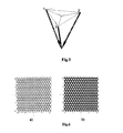
Fig. 5 - The scheme of the symmetrical layout of the three interfering laser beams. -
Fig. 6 - Images of the periodic structures obtained by forming with the symmetrically arranged three interfering laser beams according toFig.5 , when Δϕ = 0 and Ith = I0 x 11% (a) and Ith = I0 x 50% (b). -
Fig. 7 - The scheme of the symmetrical layout of the six interfering laser beams. -
Fig. 8 - Images of the periodic structures obtained by forming with the symmetrically arranged six interfering laser beams according toFig. 7 , when Δϕ = 0 and Ith = I0 x 6% (a) and Ith = I0 x 11% (b). -
Fig. 9 - The scheme of the layout of the three symmetrically arranged beams and the central beam. -
Fig. 10 - Images of the periodic structures obtained by forming with the symmetrically arranged three interfering laser beams and the central beam according toFig. 9 , when Δϕ = 0, Δz = 0 and Ith = I0 x 6% (a) and Ith = I0 x 11% (b). -
Fig. 11 - The scheme of the layout of the six symmetrically arranged beams and the central beam. -
Fig. 12 - Images of the periodic structures obtained by forming with the symmetrically arranged six interfering laser beams and the central beam according toFig. 11 , when Δϕ = 0, Δ z = 0 and Ith = I0 x 1.5% (a) and Ith = I0 x 7% (b). -
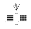
Fig. 13 - The scheme of the layout of the four symmetrically arranged beams and the central beam. -
Fig. 14 - Images of the periodic structures obtained by forming with the symmetrically arranged four interfering laser beams and the central beam according toFig. 13 , when Δϕ = π/2, Ith = I0 x 40%, Δ z = 0 (a) and Δ z = 0.2 period in the z direction (b). - The proposed method for formation of periodical structures comprises the following sequence of operations. The pulse laser beam is split into a chosen number of beams from 3 to 6, i.e. three, four or six, and they are directed into a thin film deposited on the substrate material, symmetrically in respect to the normal to the surface of the film, in such a way that, they interfere there by forming a periodic intensity distribution of laser radiation. The total intensity of the interfering laser beams is chosen so that it is higher than the ablation threshold of the said film Ith , while the ablation threshold of the film would be between about 50% to about 1.5% of the intensity I0 formed at the maxima of the interference distribution. Changes of the said total intensity within the specified limits to the extent that are required for the formation of the selected periodic structure images. The said interference image can be additionally changed by choosing the phase difference Δϕ between the interfering laser beams. Besides, the said image can be changed by directing the central laser beam along the direction of the symmetry axis of the interfering beams, and/or by choosing the distance between the said film and the intersection point of the beams along the propagation direction of the central beam.
- The proposed method for formation of periodical structures in thin material films by interfering laser beams 1-6 can be realized with the device, the optical scheme of which is shown in
Fig. 1 . The device has apulsed laser 7, on the beam propagation path of which there are sequentially placed: a laser pulseenergy control unit 8, (e.g. attenuator, consisting of Pockels cell and a thin-film polarizer), a high reflecting mirror 9, a diffractiveoptical element 10 for splitting the beam into 3, 4 or 6 beams (with additionally, including or excluding the central beam), acollimating lens 11, a unit for controlling the phase difference 12 (e.g. a parallel glass plate, which can be rotated), adiaphragm 13 for beam selection, afocal lens 14, a sample 15 (thin film on the substrate), a positioning device for the sample 16 (e.g. a piezo-electric XYZ 3-axis nanopositioning system). - The scheme of interference pattern formation without the central beam is shown in
Fig. 2a , and with the central beam present is shown inFig. 2b . When the central beam is absent, the interference image does not change in the direction perpendicular to the surface of the sample z throughout the entire beam overlap zone. The central beam generates additional modulation of the intensity distribution in the z direction. Λ is the period of the interference image on the XY plane, (on the surface of the sample, the Y is perpendicular to the plane of the picture); Λ Z is the period of the interference image in the z direction, which is perpendicular to the surface of the sample; Δz is the shift along z axis (the shift of the sample with respect to the position of the focal point of the focusing lens). - Below we provide specific embodiment examples of the method, which do not limit the breadth of this patent.
- In the case of the four laser beams 1-4, symmetrically arranged according to
Fig. 3 , the intensity distribution at the interference zone can be expressed by the formula:
where Ei the electric field, ki wave vector and ϕ i phase for each out of 4 laser beams; r is a coordinate vector. The indices indicate the laser beams: 1, 2, 3 and 4. - The intensity distribution of the interference field of the symmetrically arranged beams 1-4 (
Fig.3 ) shown inFig. 4a is a regular square matrix of interference maxima, i.e. the standard periodic structure made of circular holes. - The two-dimensional lattice period Λ depends on the angle between the opposite beams:
where
- Since the optical system has a radial symmetry, therefore phases of all the interfering beams at the intersection point are the same, or the phase difference between each of the beams is equal to zero (since all the beams follow the same optical path). In order to introduce the phase difference between the beams it is necessary to create a difference in the optical path between the beams, for instance, in the path of the first beam a glass plate is placed with the thickness d and the refractive index n , while the second beam travels the same distance through free space (air), in that case the path difference for the two beams is equal to d(n-1).
- This results in a phase difference between the beams

- When the phase difference between the even (2, 4) and the odd (1, 3) beams is equal to π/2, the old maxima disappears and the new ones appear in the gaps between the former ones.
- The interference field can be altered not only by changing the phase differences between the beams. The threshold nature of film ablation creates the conditions for additional control over shape of the periodic structures formed on the metal film, and that is the technical solution sought by this invention.
- The structure, which is formed in the material film, depends not only on the arrangement of laser beams and the phase difference between the pairs of beams. The evaporation of material films is of a threshold nature: there is a minimum of laser intensity Ith , which can ablate the film over its entire thickness. Therefore, the laser intensity, which is used for irradiation, by choosing it with respect to ablation threshold, is an additional tool for controlling the form of the periodic structures. This means that the material is ablated everywhere, where the local laser intensity exceeds the threshold value of intensity Ith .
- When the phase difference Δϕ between the even (2, 4) and the odd (1, 3) beams is equal to π/2, and the threshold intensity for film ablation Ith is close to 50% level of laser intensity I0 at the interference maximum, the interference field distribution is of a "chess-board" type (
Fig. 4b ). As shown inFig. 4c ., such structure was fabricated appling a single laser pulse to a Cr film of 100 nm thickness, by precisely aligning the optical system and by choosing the laser intensity for the experiment, and by maintaining the phase difference between the even (2, 4) and the odd (1, 3) beams to be equal to π/2, while the pulse energy was 0.14 mJ. - Several types of periodic structures were modeled with computer and fabricated using a single laser pulse ablation, when four laser beams interfere. When the phase difference Δϕ between the even (2, 4) and the odd (1, 3) beams is equal to π/4, and the threshold intensity for film ablation is at 14% level of laser intensity at the interference maximum, the structure produced using the interference method is made up of rectangular elements, arranged as a segmented net with small gaps between the segments (
Fig. 4d ). - The net-like structures were obtained by evaporating a Cr film of 100 nm thickness, with a single laser pulse with the 4-beam interference, as a monotonic phase shift change was used through the interference field. (
Fig. 4e ). The fabricated structures in the metallic films on the glass substrate show that it is possible to realize in practice the interference distribution cuts at the ablation threshold. The metal was ablated locally at the places, where the laser intensity exceeds the threshold value. The periodic "chess-board" and "net"- like structures were produced experimentally, by precisely adjustment of the phase difference and the laser intensity. - A net-like structure can be realized in a film on the substrate, when the phase difference between the even (2, 4) and the odd (1, 3) beams Δϕ is equal to π/8, and the film ablation threshold is at 4% level at the maximum of the laser intensity interference (
Fig. 4f ). Such structures can be applied for the manufacturing of frequency selective structures with the spectral filtering properties within the visible light range. - In the case of three laser beams, symmetrically arranged according to
Fig. 5 , at the film ablation threshold level of 11% at the maximum of the laser intensity interference, the produced image of the formed structure is shown inFig. 6a . The periodic structure formed in this way consists of small size triangles, and it can be used as a surface plasmon antenna. - In the same case, having the film ablation threshold at 50% level, the shape of the formed structure, produced at the maximum of the laser intensity interference, is shown in
Fig. 6b , which is standard. - In the case of six laser beams, symmetrically arranged according to
Fig. 7 , having the film ablation threshold at 4% level, the shape of the formed structure, produced at the maximum of the laser intensity interference, is shown inFig. 8a . In the same case, having the film ablation threshold at 11% level, the shape of the formed structure, produced at the maximum of the laser intensity interference, is shown inFig. 8b . Both structures can be used for manufacturing of metamaterials with the photonic crystal properties or frequency selective surfaces. - The whole class of periodic structures can be fabricated by using the interference of several symmetrically arranged beams and the central beam. In this case, the interference distribution in addition depends on the distance between the said film and the beams' intersection point within it, along the direction of the central beam.
- In the case of three symmetrically arranged laser beams and one central beam, arranged according to
Fig. 9 , at the film ablation threshold level of 6% at the maximum of the laser intensity interference, the shape of the formed structure is shown inFig. 10a , while at the film ablation threshold level of 11% at the maximum of the laser intensity interference, the shape of the formed structure is shown inFig. 10b . - In the case of six symmetrically arranged laser beams and one central beam, arranged according to
Fig. 11 , at the film ablation threshold level of 1.5% at the maximum of the laser intensity interference, the shape of the formed structure is shown inFig. 12a , while at the film ablation threshold level of 11 % at the maximum of the laser intensity interference, the produced image of the formed structure is shown inFig. 12b . - In the case of four symmetrically arranged laser beams and one central beam, arranged according to
Fig. 13 , at the film ablation threshold level of 40% at the maximum of the laser intensity interference, and the phase difference between the even (2, 4) and the odd (1, 3) beams Δϕ is equal to π/2, the shape of the formed structure is shown inFig. 14a , when the sample is in the plane of the focusing lens's focal point (Δ z = 0 ). When the sample is moved away by Δ z = 0.2Λ Z in the z direction, having the same conditions, the shape of the formed structure is shown inFig. 14b . - All "non-standard" structures are created, when the threshold intensity of the film evaporation Ith is less than 50% of intensity I0 . at the maximum of the of the interference distribution. By "standard" structures here we refer to the ones that can be found in patents or published papers, i.e. regularly arranged circular holes in a square (4 beams) or hexagonal (3 or 6 beams) matrix.
- The stability of the formed structures over a large area requires high phase stability (alignment) and homogeneity of exposure across the entire area of interference. Shaped laser beams with flat-top can be applied in order to ensure better homogeneity of the structures. Using the short laser pulse duration of less than 100 ps, evaporation in the film takes faster than the heat transfer, therefore the structure of the interference image remains intact despite of the possible melting of the film material.
Claims (9)
- Method for formation of periodical structures in thin material films by interfering laser beams, where thin material film is laid on the substrate with different optical properties than the said film, which comprises directing of several pulsed laser beams into the said thin film, where the beams intersect with each other in such a way, that through interference they form a periodic laser beam intensity distribution, where at the high intensity zones of the interference field the material of the film is evaporated, while the remaining material forms periodic structure which corresponds to the layout of the low intensity zones, characterised in that the formed image of the periodic structures is changed by adjusting the total intensity of the interfering lasers beams directed into the film, the intensity is selected accordingly for a shape of periodic structure to be formed by satisfying the condition that the said total intensity at the maxima of the formed intensity distribution should be greater than the evaporation intensity threshold of the said film.
- Method according to claim 1, characterised in that the phase difference Δϕ between the interfering laser beams is provided.
- Method according to claims 1 or 2, characterised in that three or four, or six interfering laser beams, arranged symmetrically in respect to the normal to the film surface, are directed into the said film.
- Method according to claim 3, characterised in that the image of interference distribution can be additionally modified by directing an additional central laser beam into the said film, in the direction of the symmetry axis of the said interfering laser beams.
- Method according to claim 4, characterised in that the image of interference distribution gets additionally modified by choosing the distance Δ z between the said film and the beam intersection point within it along the propagation direction z of the central beam.
- Method according to any of the claims 1-5, characterised in that the thin film material is a metal such as chromium, aluminum, silver, copper, gold, while the substrate is a transparent material, for instance, glass.
- Method according to any of the claims 1-5, characterised in that the thin film material is an electrically conductive material, such as indium-tin oxide, while the substrate is a dielectric material such as polymer or glass.
- Method according to any of the claims 2, 3 and 6, characterised in that the substrate is glass coated with a thin chromium film, with four interfering laser beams directed at it, where depending on the desired shape of the periodic structure, the phase difference Δϕ between the opposite pairs of beams is selected between zero and π/2, while the laser intensity at the formed intensity distribution maxima is selected in such a way that the evaporation intensity threshold of the said film should be from approximately 50% up to approximately 1,5%, intensity, at the formed interference distribution maxima
- Method according to any of the claims 1-8, characterised in that the laser with short impulse duration (< 100 ps) is used for a evaporation the film material.
Applications Claiming Priority (1)
| Application Number | Priority Date | Filing Date | Title |
|---|---|---|---|
| LT2010069A LT5833B (en) | 2010-09-16 | 2010-09-16 | Method for formation of periodical structures in thin material films by interfering laser beams |
Publications (2)
| Publication Number | Publication Date |
|---|---|
| EP2431120A1 true EP2431120A1 (en) | 2012-03-21 |
| EP2431120B1 EP2431120B1 (en) | 2017-07-05 |
Family
ID=44117400
Family Applications (1)
| Application Number | Title | Priority Date | Filing Date |
|---|---|---|---|
| EP11160615.8A Active EP2431120B1 (en) | 2010-09-16 | 2011-03-31 | Method of forming periodic structures in thin films using interfering laser beams |
Country Status (3)
| Country | Link |
|---|---|
| EP (1) | EP2431120B1 (en) |
| ES (1) | ES2637475T3 (en) |
| LT (2) | LT5833B (en) |
Cited By (15)
| Publication number | Priority date | Publication date | Assignee | Title |
|---|---|---|---|---|
| JP2014124645A (en) * | 2012-12-25 | 2014-07-07 | Hamamatsu Photonics Kk | Device for generating patterned interference light |
| US20160158886A1 (en) * | 2013-07-22 | 2016-06-09 | Kitty KUMAR | Interferometric laser processing |
| CN109551110A (en) * | 2017-09-26 | 2019-04-02 | 蓝思科技(长沙)有限公司 | A kind of mobile phone 3D glassy layer cover board method of texture processing and processing unit (plant) |
| WO2019134769A1 (en) * | 2018-01-03 | 2019-07-11 | Fraunhofer-Gesellschaft zur Förderung der angewandten Forschung e.V. | Optical arrangement for direct laser interference structuring |
| US10522300B2 (en) | 2015-05-26 | 2019-12-31 | National Research Council Of Canada | Metallic surface with karstified relief, forming same, and high surface area metallic electrochemical interface |
| US20200156187A1 (en) * | 2018-11-15 | 2020-05-21 | Samsung Display Co., Ltd. | Laser apparatus and substrate etching method using the same |
| DE102018220434A1 (en) | 2018-11-28 | 2020-05-28 | Fraunhofer-Gesellschaft zur Förderung der angewandten Forschung e.V. | Optical arrangement for structuring surfaces of a substrate |
| WO2020221499A1 (en) | 2019-04-30 | 2020-11-05 | Fraunhofer-Gesellschaft zur Förderung der angewandten Forschung e.V. | Arrangement for modifying surfaces of metal components |
| DE102021117204A1 (en) | 2021-07-03 | 2023-01-05 | Fusion Bionic Gmbh | Device and method for laser interference structuring of transparent substrates with periodic point structures for anti-reflection properties |
| WO2023280793A2 (en) | 2021-07-03 | 2023-01-12 | Fusion Bionic Gmbh | Apparatus and method for the laser-interference patterning of substrates with periodic dot patterns for antireflective properties |
| DE102022100271A1 (en) | 2022-01-07 | 2023-07-13 | 4Jet Microtech Gmbh | Device for interference structuring of a workpiece and method |
| LU102920B1 (en) | 2022-03-31 | 2023-10-02 | Fusion Bionic Gmbh | Device and method for laser interference structuring of substrates with periodic dot structures for anti-reflection properties |
| JPWO2023218580A1 (en) * | 2022-05-11 | 2023-11-16 | ||
| WO2023227720A1 (en) | 2022-05-25 | 2023-11-30 | Fusion Bionic Gmbh | Substrate with anti-glare properties |
| LU103057B1 (en) * | 2023-01-05 | 2024-07-05 | Fusion Bionic Gmbh | SURFACE STRUCTURED SUBSTRATE WITH IMPROVED HEAT TRANSFER |
Citations (4)
| Publication number | Priority date | Publication date | Assignee | Title |
|---|---|---|---|---|
| JPS62114138A (en) | 1985-11-13 | 1987-05-25 | Ricoh Co Ltd | Method for manufacturing a mold for duplicating information recording master discs |
| JPH1126344A (en) | 1997-06-30 | 1999-01-29 | Hitachi Ltd | Pattern forming method and apparatus and semiconductor device manufacturing method |
| JP2003025085A (en) | 2001-07-12 | 2003-01-28 | Seiko Epson Corp | Laser processing method and laser processing apparatus |
| CN1603888A (en) | 2004-11-05 | 2005-04-06 | 中国科学院上海光学精密机械研究所 | Method for transmitting periodic microstructure by femtosecond laser coherence technology |
Family Cites Families (1)
| Publication number | Priority date | Publication date | Assignee | Title |
|---|---|---|---|---|
| DE102006023940B4 (en) * | 2006-05-19 | 2009-06-10 | Laser-Laboratorium Göttingen e.V. | Process for nanostructuring of a substrate |
-
2010
- 2010-09-16 LT LT2010069A patent/LT5833B/en not_active IP Right Cessation
-
2011
- 2011-03-31 ES ES11160615.8T patent/ES2637475T3/en active Active
- 2011-03-31 EP EP11160615.8A patent/EP2431120B1/en active Active
- 2011-03-31 LT LTEP11160615.8T patent/LT2431120T/en unknown
Patent Citations (4)
| Publication number | Priority date | Publication date | Assignee | Title |
|---|---|---|---|---|
| JPS62114138A (en) | 1985-11-13 | 1987-05-25 | Ricoh Co Ltd | Method for manufacturing a mold for duplicating information recording master discs |
| JPH1126344A (en) | 1997-06-30 | 1999-01-29 | Hitachi Ltd | Pattern forming method and apparatus and semiconductor device manufacturing method |
| JP2003025085A (en) | 2001-07-12 | 2003-01-28 | Seiko Epson Corp | Laser processing method and laser processing apparatus |
| CN1603888A (en) | 2004-11-05 | 2005-04-06 | 中国科学院上海光学精密机械研究所 | Method for transmitting periodic microstructure by femtosecond laser coherence technology |
Non-Patent Citations (5)
| Title |
|---|
| "Proceedings of the SPIE", vol. 5662, 2004, BELLINGHAM WA, US, article NAKATA Y; OKADA T; MAEDA M: "Generation of nanosized materials by processing of thin film by interfering femtosecond laser beams", pages: 749 - 754, XP040194075 * |
| LASAGNI A F ET AL: "Direct fabrication of periodic patterns with hierarchical sub-wavelength structures on poly(3,4-ethylene dioxythiophene)poly(styrene sulfonate) thin films using femtosecond laser interference patterning", APPLIED SURFACE SCIENCE, ELSEVIER, AMSTERDAM, NL, vol. 256, no. 6, 1 January 2010 (2010-01-01), pages 1708 - 1713, XP026820494, ISSN: 0169-4332, [retrieved on 20091006] * |
| MÄDER M ET AL: "Large area metal dot matrices made by diffraction mask projection laser ablation", PHYSICA STATUS SOLIDI (RRL) - RAPID RESEARCH LETTERS WILEY-VCH VERLAG GMBH GERMANY, vol. 2, no. 1, January 2008 (2008-01-01), pages 34 - 36, XP002664743, ISSN: 1862-6254 * |
| MOLOTOKAITE E ET AL: "Picosecond laser beam interference ablation of thin metal films on glass substrate", JOURNAL OF LASER MICRO/NANOENGINEERING, JAPAN LASER PROCESSING SOCIETY, JP, vol. 5, no. 1, February 2010 (2010-02-01), pages 74 - 79, XP002664674, DOI: 10.2961/JLMN.2010.01.0016 * |
| ZHAO QUAN-ZHONG ET AL: "Formation of arrayed holes on metal foil and metal film by multibeam interfering femtosecond laser beams", CHINESE PHYSICS, INSTITUTE OF PHYSICS PUBLISHING, BRISTOL, UK, vol. 14, no. 6, 1 June 2005 (2005-06-01), pages 1181 - 1184, XP020092474, ISSN: 1009-1963, DOI: 10.1088/1009-1963/14/6/021 * |
Cited By (27)
| Publication number | Priority date | Publication date | Assignee | Title |
|---|---|---|---|---|
| JP2014124645A (en) * | 2012-12-25 | 2014-07-07 | Hamamatsu Photonics Kk | Device for generating patterned interference light |
| US20160158886A1 (en) * | 2013-07-22 | 2016-06-09 | Kitty KUMAR | Interferometric laser processing |
| KR20160067830A (en) * | 2013-07-22 | 2016-06-14 | 키티 쿠마 | Interferometric laser processing |
| JP2016531002A (en) * | 2013-07-22 | 2016-10-06 | クマー,キティー | Interferometric laser processing |
| US10522300B2 (en) | 2015-05-26 | 2019-12-31 | National Research Council Of Canada | Metallic surface with karstified relief, forming same, and high surface area metallic electrochemical interface |
| CN109551110A (en) * | 2017-09-26 | 2019-04-02 | 蓝思科技(长沙)有限公司 | A kind of mobile phone 3D glassy layer cover board method of texture processing and processing unit (plant) |
| WO2019134769A1 (en) * | 2018-01-03 | 2019-07-11 | Fraunhofer-Gesellschaft zur Förderung der angewandten Forschung e.V. | Optical arrangement for direct laser interference structuring |
| US11370061B2 (en) | 2018-01-03 | 2022-06-28 | Fraunhofer-Gesellschaft Zur Foerderung Der Angewandten Forshung E.V. | Optical arrangement for direct laser interference structuring |
| US11752577B2 (en) * | 2018-11-15 | 2023-09-12 | Samsung Display Co., Ltd. | Laser apparatus and substrate etching method using the same |
| US20200156187A1 (en) * | 2018-11-15 | 2020-05-21 | Samsung Display Co., Ltd. | Laser apparatus and substrate etching method using the same |
| CN111185677A (en) * | 2018-11-15 | 2020-05-22 | 三星显示有限公司 | Laser apparatus and substrate etching method using the same |
| KR20200057157A (en) * | 2018-11-15 | 2020-05-26 | 삼성디스플레이 주식회사 | Laser apparatus and substrate etching method using the same |
| CN111185677B (en) * | 2018-11-15 | 2024-05-10 | 三星显示有限公司 | Laser device and substrate etching method using the same |
| DE102018220434A1 (en) | 2018-11-28 | 2020-05-28 | Fraunhofer-Gesellschaft zur Förderung der angewandten Forschung e.V. | Optical arrangement for structuring surfaces of a substrate |
| EP3660573A1 (en) | 2018-11-28 | 2020-06-03 | FRAUNHOFER-GESELLSCHAFT zur Förderung der angewandten Forschung e.V. | Optical arrangement for structuring surfaces of a substrate |
| WO2020221499A1 (en) | 2019-04-30 | 2020-11-05 | Fraunhofer-Gesellschaft zur Förderung der angewandten Forschung e.V. | Arrangement for modifying surfaces of metal components |
| DE102019206179B4 (en) | 2019-04-30 | 2023-06-07 | Fraunhofer-Gesellschaft zur Förderung der angewandten Forschung e.V. | Arrangement for modifying surfaces of metallic components |
| DE102019206179A1 (en) * | 2019-04-30 | 2020-11-05 | Fraunhofer-Gesellschaft zur Förderung der angewandten Forschung e.V. | Arrangement for modifying the surfaces of metallic components |
| WO2023280793A2 (en) | 2021-07-03 | 2023-01-12 | Fusion Bionic Gmbh | Apparatus and method for the laser-interference patterning of substrates with periodic dot patterns for antireflective properties |
| DE102021117204A1 (en) | 2021-07-03 | 2023-01-05 | Fusion Bionic Gmbh | Device and method for laser interference structuring of transparent substrates with periodic point structures for anti-reflection properties |
| DE102022100271A1 (en) | 2022-01-07 | 2023-07-13 | 4Jet Microtech Gmbh | Device for interference structuring of a workpiece and method |
| LU102920B1 (en) | 2022-03-31 | 2023-10-02 | Fusion Bionic Gmbh | Device and method for laser interference structuring of substrates with periodic dot structures for anti-reflection properties |
| JPWO2023218580A1 (en) * | 2022-05-11 | 2023-11-16 | ||
| WO2023218580A1 (en) * | 2022-05-11 | 2023-11-16 | 株式会社ニコン | Processing optical system, processing device, and processing method |
| WO2023227720A1 (en) | 2022-05-25 | 2023-11-30 | Fusion Bionic Gmbh | Substrate with anti-glare properties |
| LU103057B1 (en) * | 2023-01-05 | 2024-07-05 | Fusion Bionic Gmbh | SURFACE STRUCTURED SUBSTRATE WITH IMPROVED HEAT TRANSFER |
| WO2024146963A1 (en) * | 2023-01-05 | 2024-07-11 | Fusion Bionic Gmbh | Surface-structured substrate with improved heat transfer |
Also Published As
| Publication number | Publication date |
|---|---|
| LT2010069A (en) | 2012-03-26 |
| ES2637475T3 (en) | 2017-10-13 |
| EP2431120B1 (en) | 2017-07-05 |
| LT5833B (en) | 2012-05-25 |
| LT2431120T (en) | 2017-08-25 |
Similar Documents
| Publication | Publication Date | Title |
|---|---|---|
| EP2431120B1 (en) | Method of forming periodic structures in thin films using interfering laser beams | |
| US12313953B2 (en) | Phase front shaping in one and two-dimensional optical phased arrays | |
| EP0656241B1 (en) | Apparatus and method for laser machining | |
| Indrišiūnas et al. | Two complementary ways of thin-metal-film patterning using laser beam interference and direct ablation | |
| JP2003025085A (en) | Laser processing method and laser processing apparatus | |
| US11468912B2 (en) | Device and arrangement for controlling an electromagnetic wave, methods of forming and operating the same | |
| JPWO1994029069A1 (en) | Laser processing device, laser processing method, and liquid crystal panel | |
| Guo et al. | Mid-infrared polarization devices based on the double-phase modulating dielectric metasurface | |
| JP2007509361A (en) | Phase angle control type fixed element for long wavelength electromagnetic wave | |
| Voisiat et al. | Picosecond-laser 4-beam-interference ablation as a flexible tool for thin film microstructuring | |
| Dayal et al. | Flexible metamaterial absorbers with multi-band infrared response | |
| Smayev et al. | Direct single-pass writing of two-phase binary diffraction gratings in a Ge2Sb2Te5 thin film by femtosecond laser pulses | |
| Šlevas et al. | An optical needle with elongated transversal profile created using Airy beams for laser processing of glasses | |
| Geng et al. | Quasicylindrical waves for ordered nanostructuring | |
| JP2009192609A (en) | Polarization control element | |
| CN113391379A (en) | Terahertz regulating and controlling device, preparation method, vector light beam generator and design method | |
| Voisiat et al. | Band-pass filters for THz spectral range fabricated by laser ablation | |
| Mauclair et al. | Dynamic spatial beam shaping for ultrafast laser processing: a review | |
| Nivas et al. | Femtosecond laser direct writing of complementary THz metasurfaces using a structured vortex beam | |
| JP6221849B2 (en) | Exposure method, method for manufacturing fine periodic structure, method for manufacturing grid polarizing element, and exposure apparatus | |
| JP2005205464A (en) | Laser processing method, structure and optical element | |
| Voisiat | Flexible microstructuring of thin films using multi-beam interference ablation with ultrashort lasers | |
| Zhao et al. | Hybrid grating-hole nanostructures produced by spatiotemporal modulation of femtosecond lasers: implications for near-field enhancement | |
| EP3519868A1 (en) | A meta-material, devices and methods of use thereof | |
| KR102685763B1 (en) | Method for producing a light deflecting structure, use of a substrate having such a light deflecting structure, and a light deflecting unit having such a light deflecting structure |
Legal Events
| Date | Code | Title | Description |
|---|---|---|---|
| PUAI | Public reference made under article 153(3) epc to a published international application that has entered the european phase |
Free format text: ORIGINAL CODE: 0009012 |
|
| 17P | Request for examination filed |
Effective date: 20110602 |
|
| AK | Designated contracting states |
Kind code of ref document: A1 Designated state(s): AL AT BE BG CH CY CZ DE DK EE ES FI FR GB GR HR HU IE IS IT LI LT LU LV MC MK MT NL NO PL PT RO RS SE SI SK SM TR |
|
| AX | Request for extension of the european patent |
Extension state: BA ME |
|
| GRAP | Despatch of communication of intention to grant a patent |
Free format text: ORIGINAL CODE: EPIDOSNIGR1 |
|
| INTG | Intention to grant announced |
Effective date: 20170418 |
|
| RAP1 | Party data changed (applicant data changed or rights of an application transferred) |
Owner name: VALSTYBINIS MOKSLINIU TYRIMU INSTITUTAS FIZINIU IR |
|
| GRAS | Grant fee paid |
Free format text: ORIGINAL CODE: EPIDOSNIGR3 |
|
| GRAA | (expected) grant |
Free format text: ORIGINAL CODE: 0009210 |
|
| AK | Designated contracting states |
Kind code of ref document: B1 Designated state(s): AL AT BE BG CH CY CZ DE DK EE ES FI FR GB GR HR HU IE IS IT LI LT LU LV MC MK MT NL NO PL PT RO RS SE SI SK SM TR |
|
| REG | Reference to a national code |
Ref country code: GB Ref legal event code: FG4D |
|
| REG | Reference to a national code |
Ref country code: CH Ref legal event code: EP |
|
| REG | Reference to a national code |
Ref country code: AT Ref legal event code: REF Ref document number: 906261 Country of ref document: AT Kind code of ref document: T Effective date: 20170715 |
|
| REG | Reference to a national code |
Ref country code: IE Ref legal event code: FG4D |
|
| REG | Reference to a national code |
Ref country code: DE Ref legal event code: R096 Ref document number: 602011039252 Country of ref document: DE |
|
| REG | Reference to a national code |
Ref country code: ES Ref legal event code: FG2A Ref document number: 2637475 Country of ref document: ES Kind code of ref document: T3 Effective date: 20171013 |
|
| REG | Reference to a national code |
Ref country code: NL Ref legal event code: MP Effective date: 20170705 |
|
| REG | Reference to a national code |
Ref country code: AT Ref legal event code: MK05 Ref document number: 906261 Country of ref document: AT Kind code of ref document: T Effective date: 20170705 |
|
| PG25 | Lapsed in a contracting state [announced via postgrant information from national office to epo] |
Ref country code: SE Free format text: LAPSE BECAUSE OF FAILURE TO SUBMIT A TRANSLATION OF THE DESCRIPTION OR TO PAY THE FEE WITHIN THE PRESCRIBED TIME-LIMIT Effective date: 20170705 Ref country code: NL Free format text: LAPSE BECAUSE OF FAILURE TO SUBMIT A TRANSLATION OF THE DESCRIPTION OR TO PAY THE FEE WITHIN THE PRESCRIBED TIME-LIMIT Effective date: 20170705 Ref country code: AT Free format text: LAPSE BECAUSE OF FAILURE TO SUBMIT A TRANSLATION OF THE DESCRIPTION OR TO PAY THE FEE WITHIN THE PRESCRIBED TIME-LIMIT Effective date: 20170705 Ref country code: NO Free format text: LAPSE BECAUSE OF FAILURE TO SUBMIT A TRANSLATION OF THE DESCRIPTION OR TO PAY THE FEE WITHIN THE PRESCRIBED TIME-LIMIT Effective date: 20171005 Ref country code: FI Free format text: LAPSE BECAUSE OF FAILURE TO SUBMIT A TRANSLATION OF THE DESCRIPTION OR TO PAY THE FEE WITHIN THE PRESCRIBED TIME-LIMIT Effective date: 20170705 Ref country code: HR Free format text: LAPSE BECAUSE OF FAILURE TO SUBMIT A TRANSLATION OF THE DESCRIPTION OR TO PAY THE FEE WITHIN THE PRESCRIBED TIME-LIMIT Effective date: 20170705 |
|
| PG25 | Lapsed in a contracting state [announced via postgrant information from national office to epo] |
Ref country code: IS Free format text: LAPSE BECAUSE OF FAILURE TO SUBMIT A TRANSLATION OF THE DESCRIPTION OR TO PAY THE FEE WITHIN THE PRESCRIBED TIME-LIMIT Effective date: 20171105 Ref country code: RS Free format text: LAPSE BECAUSE OF FAILURE TO SUBMIT A TRANSLATION OF THE DESCRIPTION OR TO PAY THE FEE WITHIN THE PRESCRIBED TIME-LIMIT Effective date: 20170705 Ref country code: BG Free format text: LAPSE BECAUSE OF FAILURE TO SUBMIT A TRANSLATION OF THE DESCRIPTION OR TO PAY THE FEE WITHIN THE PRESCRIBED TIME-LIMIT Effective date: 20171005 Ref country code: LV Free format text: LAPSE BECAUSE OF FAILURE TO SUBMIT A TRANSLATION OF THE DESCRIPTION OR TO PAY THE FEE WITHIN THE PRESCRIBED TIME-LIMIT Effective date: 20170705 Ref country code: PL Free format text: LAPSE BECAUSE OF FAILURE TO SUBMIT A TRANSLATION OF THE DESCRIPTION OR TO PAY THE FEE WITHIN THE PRESCRIBED TIME-LIMIT Effective date: 20170705 Ref country code: GR Free format text: LAPSE BECAUSE OF FAILURE TO SUBMIT A TRANSLATION OF THE DESCRIPTION OR TO PAY THE FEE WITHIN THE PRESCRIBED TIME-LIMIT Effective date: 20171006 |
|
| REG | Reference to a national code |
Ref country code: FR Ref legal event code: PLFP Year of fee payment: 8 |
|
| REG | Reference to a national code |
Ref country code: DE Ref legal event code: R097 Ref document number: 602011039252 Country of ref document: DE |
|
| PG25 | Lapsed in a contracting state [announced via postgrant information from national office to epo] |
Ref country code: DK Free format text: LAPSE BECAUSE OF FAILURE TO SUBMIT A TRANSLATION OF THE DESCRIPTION OR TO PAY THE FEE WITHIN THE PRESCRIBED TIME-LIMIT Effective date: 20170705 Ref country code: CZ Free format text: LAPSE BECAUSE OF FAILURE TO SUBMIT A TRANSLATION OF THE DESCRIPTION OR TO PAY THE FEE WITHIN THE PRESCRIBED TIME-LIMIT Effective date: 20170705 Ref country code: RO Free format text: LAPSE BECAUSE OF FAILURE TO SUBMIT A TRANSLATION OF THE DESCRIPTION OR TO PAY THE FEE WITHIN THE PRESCRIBED TIME-LIMIT Effective date: 20170705 |
|
| PLBE | No opposition filed within time limit |
Free format text: ORIGINAL CODE: 0009261 |
|
| STAA | Information on the status of an ep patent application or granted ep patent |
Free format text: STATUS: NO OPPOSITION FILED WITHIN TIME LIMIT |
|
| PG25 | Lapsed in a contracting state [announced via postgrant information from national office to epo] |
Ref country code: SM Free format text: LAPSE BECAUSE OF FAILURE TO SUBMIT A TRANSLATION OF THE DESCRIPTION OR TO PAY THE FEE WITHIN THE PRESCRIBED TIME-LIMIT Effective date: 20170705 Ref country code: SK Free format text: LAPSE BECAUSE OF FAILURE TO SUBMIT A TRANSLATION OF THE DESCRIPTION OR TO PAY THE FEE WITHIN THE PRESCRIBED TIME-LIMIT Effective date: 20170705 Ref country code: IT Free format text: LAPSE BECAUSE OF FAILURE TO SUBMIT A TRANSLATION OF THE DESCRIPTION OR TO PAY THE FEE WITHIN THE PRESCRIBED TIME-LIMIT Effective date: 20170705 Ref country code: EE Free format text: LAPSE BECAUSE OF FAILURE TO SUBMIT A TRANSLATION OF THE DESCRIPTION OR TO PAY THE FEE WITHIN THE PRESCRIBED TIME-LIMIT Effective date: 20170705 |
|
| 26N | No opposition filed |
Effective date: 20180406 |
|
| PG25 | Lapsed in a contracting state [announced via postgrant information from national office to epo] |
Ref country code: SI Free format text: LAPSE BECAUSE OF FAILURE TO SUBMIT A TRANSLATION OF THE DESCRIPTION OR TO PAY THE FEE WITHIN THE PRESCRIBED TIME-LIMIT Effective date: 20170705 |
|
| REG | Reference to a national code |
Ref country code: CH Ref legal event code: PL |
|
| PG25 | Lapsed in a contracting state [announced via postgrant information from national office to epo] |
Ref country code: MC Free format text: LAPSE BECAUSE OF FAILURE TO SUBMIT A TRANSLATION OF THE DESCRIPTION OR TO PAY THE FEE WITHIN THE PRESCRIBED TIME-LIMIT Effective date: 20170705 |
|
| REG | Reference to a national code |
Ref country code: BE Ref legal event code: MM Effective date: 20180331 |
|
| REG | Reference to a national code |
Ref country code: IE Ref legal event code: MM4A |
|
| PG25 | Lapsed in a contracting state [announced via postgrant information from national office to epo] |
Ref country code: LU Free format text: LAPSE BECAUSE OF NON-PAYMENT OF DUE FEES Effective date: 20180331 |
|
| PG25 | Lapsed in a contracting state [announced via postgrant information from national office to epo] |
Ref country code: IE Free format text: LAPSE BECAUSE OF NON-PAYMENT OF DUE FEES Effective date: 20180331 |
|
| PG25 | Lapsed in a contracting state [announced via postgrant information from national office to epo] |
Ref country code: CH Free format text: LAPSE BECAUSE OF NON-PAYMENT OF DUE FEES Effective date: 20180331 Ref country code: BE Free format text: LAPSE BECAUSE OF NON-PAYMENT OF DUE FEES Effective date: 20180331 Ref country code: LI Free format text: LAPSE BECAUSE OF NON-PAYMENT OF DUE FEES Effective date: 20180331 |
|
| PG25 | Lapsed in a contracting state [announced via postgrant information from national office to epo] |
Ref country code: MT Free format text: LAPSE BECAUSE OF NON-PAYMENT OF DUE FEES Effective date: 20180331 |
|
| PG25 | Lapsed in a contracting state [announced via postgrant information from national office to epo] |
Ref country code: TR Free format text: LAPSE BECAUSE OF FAILURE TO SUBMIT A TRANSLATION OF THE DESCRIPTION OR TO PAY THE FEE WITHIN THE PRESCRIBED TIME-LIMIT Effective date: 20170705 |
|
| PG25 | Lapsed in a contracting state [announced via postgrant information from national office to epo] |
Ref country code: PT Free format text: LAPSE BECAUSE OF FAILURE TO SUBMIT A TRANSLATION OF THE DESCRIPTION OR TO PAY THE FEE WITHIN THE PRESCRIBED TIME-LIMIT Effective date: 20170705 Ref country code: HU Free format text: LAPSE BECAUSE OF FAILURE TO SUBMIT A TRANSLATION OF THE DESCRIPTION OR TO PAY THE FEE WITHIN THE PRESCRIBED TIME-LIMIT; INVALID AB INITIO Effective date: 20110331 |
|
| PG25 | Lapsed in a contracting state [announced via postgrant information from national office to epo] |
Ref country code: CY Free format text: LAPSE BECAUSE OF FAILURE TO SUBMIT A TRANSLATION OF THE DESCRIPTION OR TO PAY THE FEE WITHIN THE PRESCRIBED TIME-LIMIT Effective date: 20170705 Ref country code: MK Free format text: LAPSE BECAUSE OF NON-PAYMENT OF DUE FEES Effective date: 20170705 |
|
| PG25 | Lapsed in a contracting state [announced via postgrant information from national office to epo] |
Ref country code: AL Free format text: LAPSE BECAUSE OF FAILURE TO SUBMIT A TRANSLATION OF THE DESCRIPTION OR TO PAY THE FEE WITHIN THE PRESCRIBED TIME-LIMIT Effective date: 20170705 |
|
| PGFP | Annual fee paid to national office [announced via postgrant information from national office to epo] |
Ref country code: LT Payment date: 20240206 Year of fee payment: 14 |
|
| PGFP | Annual fee paid to national office [announced via postgrant information from national office to epo] |
Ref country code: ES Payment date: 20250416 Year of fee payment: 15 |
|
| REG | Reference to a national code |
Ref country code: LT Ref legal event code: MM4D Effective date: 20250331 |
|
| PG25 | Lapsed in a contracting state [announced via postgrant information from national office to epo] |
Ref country code: LT Free format text: LAPSE BECAUSE OF NON-PAYMENT OF DUE FEES Effective date: 20250331 |
|
| PGFP | Annual fee paid to national office [announced via postgrant information from national office to epo] |
Ref country code: GB Payment date: 20260209 Year of fee payment: 16 |
|
| PGFP | Annual fee paid to national office [announced via postgrant information from national office to epo] |
Ref country code: DE Payment date: 20260217 Year of fee payment: 16 |
|
| PGFP | Annual fee paid to national office [announced via postgrant information from national office to epo] |
Ref country code: FR Payment date: 20260209 Year of fee payment: 16 |