EP2437291A2 - Wiring design system of semiconductor integrated circuit, semiconductor integrated circuit, and wiring design program - Google Patents
Wiring design system of semiconductor integrated circuit, semiconductor integrated circuit, and wiring design program Download PDFInfo
- Publication number
- EP2437291A2 EP2437291A2 EP11184277A EP11184277A EP2437291A2 EP 2437291 A2 EP2437291 A2 EP 2437291A2 EP 11184277 A EP11184277 A EP 11184277A EP 11184277 A EP11184277 A EP 11184277A EP 2437291 A2 EP2437291 A2 EP 2437291A2
- Authority
- EP
- European Patent Office
- Prior art keywords
- clock wiring
- clock
- grid
- flip flop
- semiconductor integrated
- Prior art date
- Legal status (The legal status is an assumption and is not a legal conclusion. Google has not performed a legal analysis and makes no representation as to the accuracy of the status listed.)
- Withdrawn
Links
Images


Classifications
-
- G—PHYSICS
- G06—COMPUTING OR CALCULATING; COUNTING
- G06F—ELECTRIC DIGITAL DATA PROCESSING
- G06F1/00—Details not covered by groups G06F3/00 - G06F13/00 and G06F21/00
- G06F1/26—Power supply means, e.g. regulation thereof
- G06F1/32—Means for saving power
-
- G—PHYSICS
- G06—COMPUTING OR CALCULATING; COUNTING
- G06F—ELECTRIC DIGITAL DATA PROCESSING
- G06F30/00—Computer-aided design [CAD]
- G06F30/30—Circuit design
- G06F30/39—Circuit design at the physical level
- G06F30/394—Routing
-
- G—PHYSICS
- G06—COMPUTING OR CALCULATING; COUNTING
- G06F—ELECTRIC DIGITAL DATA PROCESSING
- G06F30/00—Computer-aided design [CAD]
- G06F30/30—Circuit design
- G06F30/39—Circuit design at the physical level
- G06F30/396—Clock trees
-
- G—PHYSICS
- G06—COMPUTING OR CALCULATING; COUNTING
- G06F—ELECTRIC DIGITAL DATA PROCESSING
- G06F2119/00—Details relating to the type or aim of the analysis or the optimisation
- G06F2119/06—Power analysis or power optimisation
Definitions
- the present invention relates to a wiring design system for semiconductor integrated circuit, and more particularly, to a wiring design system for semiconductor integrated circuit, a semiconductor integrated circuit, and a wiring design program which realize a low power consumption in a grid-shaped clock wiring.
- the clock wiring of a semiconductor integrated circuit of related art is formed by the grid-shaped clock wiring in which clock wiring lines are uniformly arranged in a grid pattern.
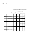
- Fig. 12 is a view showing an example of a clock wiring line 50 of a semiconductor integrated circuit 40 according to the related art technique.
- the clock wiring line 50 in a uniform grid pattern has the following characteristics. Namely, time difference among the clock signals which arrive at the respective flip flop circuits becomes less because the clock wiring lines are uniformly arranged in a grid pattern. A difference between the first clock signal arriving at a flip flop circuit at first and the last clock signal arriving at another flip flop circuit at last is called a clock skew.
- Fig. 13 is a view for describing the effect of the clock skew on the data signal propagation.
- FF flip flop circuits
- FF 521 and FF 522 flip flop circuits
- clock signals are supplied there.
- Time of the data signal propagation between the both is designed to be ten times as long as a clock cycle.
- the arrival time of a clock signal to each of the FF 521 and the FF 522 is shown as +2 by the clock cycle and there is no clock skew.
- the data signal propagation time is shown as 10 by the clock cycle and there occurs no problem.
- the grid-shaped clock wiring for distributing the clocks to the semiconductor integrated circuit 40 is formed in a uniform grid shape in order to reduce the clock skew, there is a problem that some redundant line may occur in the grid.
- the intervals in the grid becomes an important matter. It is because, when the spaces between grids are narrow, the uniformity of the clock distribution increases, but the number of the redundant lines increases and accordingly the power consumption increases. While, when the spaces between grids are wide, the number of the redundant lines decreases, but the uniformity of the clock distribution is deteriorated. Since an effective means for determining the intervals in the grid is not established, it is difficult to determine the intervals in the grid.
- Patent Document 1 Japanese Patent Publication Laid-Open No. 2003-282712 (Patent Document 1) and No. 2002-43550 (Patent Document 2).
- a method disclosed in Patent Document 1 provides a clock wiring method for creating a grid-shaped clock wiring corresponding to a hierarchical structure of a semiconductor chip layout while preserving the hierarchical structure of the semiconductor chip.
- clocks are distributed so that the clock skew from an external clock input terminal to a flip flop circuit forming every circuit block may be minimum and the clock signal is supplied to every flip flop circuit forming the circuit block.
- a method disclosed in Patent Document 2 relates to a method for reducing a clock skew in a semiconductor integrated circuit, in which the number of stages of transistors in each clock driver circuit is properly arranged according to the density of the cells using the clock signals in the vicinity of a plurality of clock driver circuits of supplying a proper clock signal to a cell using a clock signal, through the grid-shaped clock wiring in a core region of the semiconductor integrated circuit.
- Patent Document 1 assumes that the structure of the grid-shaped clock wiring is not changed and it does not solve the defect of the grid-shaped clock wiring, that is the large power consumption.
- the number of the stages of the transistors in each clock driver circuit is properly arranged according to the density of the cells using the clock signals in the vicinity of a plurality of the clock driver circuits of supplying a proper clock signal to the cell using the clock signal, thereby further reducing a clock skew easily without rearrangement of the cells in the core region other than the clock driver circuit.
- Patent Document 2 also assumes that the structure of the grid-shaped clock wiring is not changed and it does not solve the defect of the grid-shaped wiring, that is the large power consumption.
- An exemplary object of the invention is to provide a wiring design system for semiconductor integrated circuit, a semiconductor integrated circuit, and a wiring design program which solve the above defect of the related art technique and realize a low power consumption in the grid-shaped clock wiring.
- a wiring design system for semiconductor integrated circuit which designs a grid-shaped clock wiring for uniformly distributing clock signals to flip flop circuits arranged within the semiconductor integrated circuit, wherein a clock wiring line having a smaller effect on distribution operation of the clock signals in the grid-shaped clock wiring is selected from clock wiring lines forming the grid-shaped clock wiring as a less necessary clock wiring line and thinned out.
- the less necessary clock wiring line is selected based on, at least one of the number of the flip flop circuits supplying the clock signals through the clock wiring lines, the number of the flip flop circuits arranged in each grid forming the grid-shaped clock wiring, and the disposition of the flip flop circuits within the semiconductor integrated circuit.
- the power consumption in the grid-shaped clock wiring can be reduced.
- the invention rearranges the flip flop circuit which becomes far from the clock wiring line receiving the clock signal, in the vicinity of the clock wiring line.
- the clock skew can be reduced to the same degree as that before thinning out of the clock wiring line.
- the power consumption in the clock wiring can be reduced while keeping the clock skew small.
- a dummy line is inserted in a portion in which a line is eliminated through thinning out.
- signal does not travel, but since the line is the same as the clock wiring line completely, the distribution of the line capacity within the semiconductor integrated circuit according to the grid-shaped clock wiring can be uniformly kept in the same way as that before thinning out of the clock wiring line.
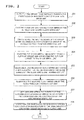
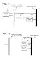
- Fig. 1 is a block diagram showing a structure of a wiring design system 10 for semiconductor integrated circuit according to a first exemplary embodiment.
- a wiring design system 10 for semiconductor integrated circuit includes a semiconductor integrated circuit design data input unit 11, an initially grid-shaped clock wiring unit 12, an initially overall elements disposing unit 13, a thinning-out clock wiring line selecting unit 14, a clock wiring line thinning-out unit 15, an arrangement wiring unit 16, and a semiconductor integrated circuit design data output unit 17.
- the semiconductor integrated circuit design data input unit 11 inputs semiconductor integrated circuit design data 101 within an input design data file 100.
- the initially grid-shaped clock wiring unit 12 can set a uniform grid-shaped clock wiring initially on the whole semiconductor integrated circuit.
- the initial condition of the clock wiring may be obtained by generating uniform grid-shaped clock wiring lines on the semiconductor integrated circuit.
- the initially overall elements disposing unit 13 can arrange all the elements on the semiconductor integrated circuit so that they can keep a specified condition.
- the thinning-out clock wiring line selecting unit 14 can select a line to be eliminated through thinning out, from the grid-shaped clock wiring (hereinafter, elimination through thinning out is abbreviated as thinning-out elimination) based on the condition of the grid-shaped clock wiring uniformly generated on the whole semiconductor integrated circuit and all the arranged elements, and output the target line for thinning-out elimination.
- the clock wiring line thinning-out unit 15 can actually thin out and eliminate the target clock wiring line for thinning-out elimination which is output by the thinning-out clock wiring line selecting unit 14, from the design data of the semiconductor integrated device.
- the arrangement wiring unit 16 can determine the disposition of all the elements and the wiring after determination of the clock wiring lines.
- the semiconductor integrated circuit design data output unit 17 supplies semiconductor integrated circuit design data 111 for manufacture with the clock wiring generated by the above unit and the position of the flip flop circuit modified, to the output design data file 110.
- a function for selecting a less necessary clock wiring line by the thinning-out clock wiring line selecting unit 14 and thinning out/eliminating the line by the clock wiring line thinning-out unit 15, which is the characteristic of the invention, may be realized by mounting a circuit component including a program for realizing such a function in a computer.
- a program (application) for realizing the characteristic function of the invention may be stored in a storing medium and the program may be executed by a computer, thereby making the computer work as the wiring design system 10 for semiconductor integrated circuit.
- Fig. 2 is a flow chart for describing the operation of the wiring design system 10 for semiconductor integrated circuit according to this exemplary embodiment.
- the semiconductor integrated circuit design data 101 that is the circuit data to be installed is supplied through the semiconductor integrated circuit design data input unit 11 (Step 201).
- the initially grid-shaped clock wiring unit 12 In order to set the initial condition of the clock wiring, the initially grid-shaped clock wiring unit 12 generates the uniform grid-shaped clock wiring lines (Step 202).
- the initially overall elements disposing unit 13 disposes all the elements of the circuit supplied through the semiconductor integrated circuit design data input unit 11 within the semiconductor integrated circuit (Step 203).
- the initially grid-shaped clock wiring unit 12 selects a clock wiring line which is nearest to each flip flop circuit and connects the flip flop circuit to the grid-shaped clock wiring as for all flip flop circuits disposed in the semiconductor integrated circuit (Step 204).
- the wiring by the initially grid-shaped clock wiring unit 12 is regarded as tentative, and a less necessary clock wiring line, having a smaller effect on the distribution of the clock signal in the grid-shaped clock wiring, is selected by using the thinning-out clock wiring line selecting unit 14 (Step 205).
- the clock wiring line thinning-out unit 15 eliminates the clock wiring line selected in this way (Step 206).
- the arrangement wiring unit 16 disposes and wires the elements of the semiconductor integrated circuit so that they may satisfy the design rule and the specification (Step 207).
- the semiconductor integrated circuit design data output unit 17 outputs the semiconductor integrated circuit design data 102 for manufacture (Step 208).
- clock wiring lines 50 are formed uniformly in the grid-shaped clock wiring.
- the grid-shaped clock wiring is generated, it is important to determine the intervals of the lines, and in the case of the invention, since a redundant grid-shaped clock wiring line is thinned out and eliminated later, a very closer interval available for use in the clock wiring line 50 may be set in advance.
- the initially overall elements disposing unit 13 disposes all the elements of the circuit supplied through the semiconductor integrated circuit design data input unit 11, within the semiconductor integrated circuit 40.
- the processing may use any conventional arrangement method.
- the thinning-out clock wiring line selecting unit 14 selects which clock wiring line 50 of the grid-shaped clock wiring is thinned out.
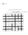
- Fig. 3 is a view showing an example of thinning out the clock wiring lines 50 uniformly according to the exemplary embodiment.
- a semiconductor integrated circuit 40 which is designed by using the wiring design system 10 for semiconductor integrated circuit, one for every two clock wiring lines 50 becomes a target clock wiring line 60 for thinning out.
- Thinning out one for every two clock wiring lines 50 as mentioned above means that the even numbers of the clock wiring lines 50 from the clock wiring line 50 positioned in the periphery of the grid-shaped clock wiring (not shown), are thinned out and eliminated from the grid-shaped clock wiring consisting of two clock wiring lines 50 crossing each other.
- Thinning out as shown in Fig. 3 is performed when the flip flop circuits are distributed uniformly. Thinning out is performed by the clock wiring line thinning-out unit 15.
- Fig. 4 is a view showing an example of thinning out the clock wiring lines 50 nonuniformly according to the exemplary embodiment.
- the target clock wiring lines 60 for thinning out are distributed nonuniformly.
- the distribution of the clock wiring lines selected by the thinning-out clock wiring line selecting unit 14 is not uniform, the distribution of the target clock wiring lines 60 for thinning out is nonuniform.
- the portion of the clock wiring line 50 which is not thinned out nor eliminated crossing the target clock wiring line 60 is not eliminated and left as shown in Fig. 4 .
- the function of the clock wiring line 50 is not damaged, it is not limited to this.
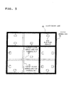
- Fig. 5 is a view showing the example of selecting the target clock wiring lines 61 and 62 according to the exemplary embodiment.
- the clock wiring lines 50 are sequentially selected in the order of increasing the number of the flip flop circuits from the clock wiring line 50 having the smallest number, and as the result, the number of the clock wiring lines 50 corresponding to a fraction of all the clock wiring lines are thinned out.
- a ratio of the target clock wiring lines for thinning out to all the clock wiring lines may be set according to the situation, but this example will be described assuming that about a quarter of the clock wiring lines 50 are thinned out.
- each of the clock wiring lines 50 excluding the target clock wiring lines 61 and 62 for thinning out supplies the clock signal to two flip flop circuits 510. While it is found that the target clock wiring line 61 for thinning out has no flip flop circuit 510 supplying the clock signal and that the target clock wiring line 62 has one flip flop circuit 510. In this case, of a total of eight clock wiring lines 50, the two target clock wiring lines 61 and 62 for thinning out having the small number of the flip flop circuits 510 supplying the clock signal, corresponding to a quarter of all the clock wiring lines, are thinned out.
- the grid-shaped clock wiring may be divided by the length of the grid.
- the length of the grid is different between the vertical line and the horizontal line.
- the clock wiring lines 50 forming the grid-shaped clock wiring is divided by the length of the grid, the number of the flip flop circuits supplying the clock signals is calculated in every clock wiring line 50, the clock wiring lines 50 are selected in the increasing order of the number of the flip flop circuits, and the number of the clock wiring lines 50 corresponding to a fraction of all clock wiring lines 50 are thinned out.
- the number of the flip flop circuits 510 arranged in the grid is calculated for every grid generated in the grid-shaped clock wiring, and the clock wiring line 50 positioned on the boundary between the grid in which the number of the flip flop circuits 510 is a predetermined number and less and the grid having the smallest number of the flip flop circuits 510, of the grids adjacent to the above grid, is thinned out.
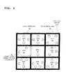
- Fig. 6 is a view for describing an example of selecting a target clock wiring line 63 for thinning out according to the exemplary embodiment.
- each of the grids 91, 92, 93, 94, 95, 96, 97, 98, and 99 has four flip flop circuits 510 and the grid 95 has one flip flop circuit 510, the smallest number of the flip flop circuits 510.
- the predetermined number When the predetermined number is set as one, it is the grid 95 that satisfies this condition. There are the four grids 92, 94, 96, and 98 that are adjacent to the grid 95 and the number of the flip flop circuits 510 arranged in each grid is four, two, three, and four respectively. The number of the flip flop circuits 510 in the grid 94 is the smallest. Therefore, the target clock wiring line 63 for thinning out positioned on the boundary between the grid 95 and the grid 94 is thinned out.
- the wiring design system 10 for semiconductor integrated circuit is a system for designing the grid-shaped clock wiring in which the clock signals are uniformly distributed to the flip flop circuits 510 arranged in the semiconductor integrated circuit 40, in which the clock wiring line 50 having a smaller effect on distribution of the clock signals is selected regarded as less necessary and thinned out, from the grid-shaped clock wiring formed by the clock wiring lines 50.
- the less necessary clock wiring line is selected based on, at least one of the number of the flip flop circuits supplying the clock signals through the clock wiring lines 50, the number of the flip flop circuits arranged in each grid forming the grid-shaped clock wiring, and the disposition of the flip flop circuits in the semiconductor integrated circuit 40.
- Fig. 7 is a view for describing the connection to the other clock wiring line 50 by the flip flop circuit 501 connected to the target clock wiring line 60 for thinning out, according to the exemplary embodiment.
- the flip flop circuit 501 which has been connected to the target clock wiring line 60 for thinning out is connected to the clock wiring line 50 which is not thinned out, through a clock signal line 80.
- a flip flop circuit 502 connected near the clock wiring line 50 which is not thinned out, there is no modification of the connection.
- the design data necessary for semiconductor manufacture can be obtained, and the semiconductor integrated circuit design data 111 for manufacture may be output by the semiconductor integrated circuit design data output unit 17.
- the electric power consumption in the grid-shaped clock wiring of the semiconductor integrated circuit 40 can be reduced.
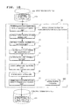
- Fig. 8 is a block diagram showing a structure of a wiring design system 20 for semiconductor integrated circuit according to the exemplary embodiment. In the following description, the important portion of Fig. 7 will be referred to.
- a flip flop circuit rearrangement unit 21 is added to the wiring design system 10 for semiconductor integrated circuit according to the first exemplary embodiment of the invention.
- the flip flop circuit rearrangement unit 21 makes the flip flop circuit 501 which becomes far from the clock wiring line 50 because the grid-shaped clock wiring is thinned out and eliminated according to the first exemplary embodiment, close to the clock wiring line 50 which is not thinned out nor eliminated, thereby restraining an increase of the clock skew caused by the thinning-out elimination of the grid-shaped clock wiring line.
- the flip flop circuit 502 since the flip flop circuit 502 is in the vicinity of the clock wiring line 50, there occurs no problem. However, since the target clock wiring line 60 for thinning out having existed in the vicinity of the flip flop circuit 501 is eliminated, the flip flop circuit 501 is connected to the clock wiring line 50 through the long clock signal line 80 and there occurs a clock skew.
- a result of checking the clock skew by an experiment and a decrease of the clock skew according to the flip flop circuit rearrangement unit 21 will be described.
- the clock skew between the flip flop circuit 501 in the vicinity of the target clock wiring line 60 for thinning out and the flip flop circuit 502 in the vicinity of the clock wiring line 50 which is not thinned out is compared between before and after thinning out of the clock wiring line 50.
- the arrangement wiring unit 16 wires the clock signal line 80 from the flip flop circuit 501 corresponding to the thinned clock wiring line 60 to the clock wiring line 50.
- the clock skew that is a difference of the arrival time of the clocks is 60 ps, while after the thinning out, it increases five times to 300 ps.
- the flip flop circuit rearrangement unit 21 rearranges the flip flop circuit 501.
- Fig. 8 is a view showing an example of the rearrangement of the flip flop circuit 501 according to the exemplary embodiment.
- the arrangement of the flip flops 501 and 502 before the rearrangement is as shown in Fig. 7 .
- the flip flop circuit 501 in the vicinity of the target clock wiring line 60 for thinning out and the flip flop circuit 502 positioned in the vicinity of the clock wiring line 50 which is not thinned out are both arranged at the same distance from the clock wiring line 50.
- the flip flop circuit 502 there is no modification of the arrangement as the result of the rearrangement.
- the flip flop circuit 501 is rearranged at a position similarly distant from the clock wiring line 50 to the flip flop circuit 502.
- the clock skew may be reduced by uniformizing the distance relation between the flip flop circuits 501 and 502 and the grid-shaped clock wiring line or by arranging the flip flop circuits 501 and 502 intensively in the vicinity of the grid-shaped clock wiring line.
- the arrangement wiring unit 16 disposes and wires the elements of the semiconductor integrated circuit 40 according to the exemplary embodiment which is designed by using the wiring design system 20 for semiconductor integrated circuit so as to satisfy the design rule and the specification.
- the semiconductor integrated circuit design data output unit 17 outputs the semiconductor integrated circuit design data 121 for manufacture to the output design data file 120.
- the flip flop circuit 501 connected to the target clock wiring line 60 for thinning out through the clock signal line 80 in Fig. 7 is arranged in the vicinity of the clock wiring line 50 as shown in Fig. 8 after the rearrangement.
- the flip flop circuit 501 is rearranged at the position across the target clock wiring line 60 on the clock signal line 80.
- the circuit may be arranged at any position between the target clock wiring line 60 and the clock wiring line 50.
- the flip flop circuit 502 may be arranged at a position closer to the clock wiring line 50 at the time of rearrangement of the flip flop circuit 501.
- the exemplary embodiment it is possible to reduce the power consumption in the clock wiring line 50 while keeping the clock skew small, by rearranging the flip flop circuit 501 after thinning out a less necessary clock wiring line.
- Fig. 10 is a block diagram showing a structure of a wiring design system 30 for semiconductor integrated circuit according to the exemplary embodiment. In the following description, the important portions of Fig. 7 will be referred to.
- a dummy wiring line inserting unit 31 is added to the wiring design system 10 according to the first exemplary embodiment of the invention.
- the dummy wiring line inserting unit 31 inserts a dummy wiring line in order to prevent the nonuniformity of the line capacity caused by the nonuniform thinning out of the clock wiring line 50 as shown in Fig. 4 .
- signal does not travel, but since it is the same wiring line as the clock wiring line 50 completely, the distribution of the line capacity in the semiconductor integrated circuit 40 can be maintained uniformly in the same way as before thinning out of the clock wiring line 50.
- the line capacity in the semiconductor integrated circuit 40 can be maintained and the signals can be analyzed and calculated easily in the same way as the ordinal grid-shaped clock wiring having the uniform capacity distribution.
- the grid-shaped clock wiring in which the capacity distribution is uniform has an advantage that the calculation of the line capacity necessary for checking the effect of signal noise is easy.
- this advantage is not lost.
- the wiring lines are thinned out nonuniformly as shown in Fig. 4 , the advantage is lost and the dummy wiring line insertion according to the exemplary embodiment is necessary.
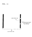
- Fig. 11 is a view showing an example of the dummy wiring line insertion according to the exemplary embodiment.
- the dummy wiring line inserting unit 31 inserts a dummy wiring line 70 for securing the capacity in a position of the clock wiring line thinned out in a way of being electrically insulated from the clock wiring line 50 not thinned out.
- the uniformity of the capacity distribution in the semiconductor integrated circuit 40 is improved and the capacity calculation can be performed with ease remarkably.
- the arrangement wiring unit 16 disposes and wires the elements of the semiconductor integrated circuit 40 according to the exemplary embodiment which is designed by using the wiring design system 30 for semiconductor integrated circuit so as to satisfy the design rule and the specification.
- the semiconductor integrated circuit design data output unit 17 outputs the semiconductor integrated circuit design data 131 for manufacture to the output design data file 130.
- the dummy wiring line 70 is inserted by the dummy wiring line inserting unit 31.
- the position of the flip flop 501 which receives the clock signal from the target clock wiring line 60 for thinning out is not changed, a clock skew is increased.
- the flip flop circuit rearrangement unit 21 rearranges the flip flop circuit as having been described in the second exemplary embodiment of the invention.
- the dummy wiring line 70 is inserted by the dummy wiring line inserting unit 31 as described in this exemplary embodiment. After the dummy wiring line 70 is inserted by the dummy wiring line inserting unit 31, the flip flop circuit may be rearranged.
- the arrangement wiring unit 16 disposes and wires the elements of the semiconductor integrated circuit 40 so as to satisfy the design rule and the specification.
- the semiconductor integrated circuit design data output unit 17 outputs the semiconductor integrated circuit design data 131 for manufacture.
- the above mentioned exemplary embodiment can prevent nonuniformity in the distribution of the line capacity within the semiconductor integrated circuit 40, caused by nonuniform thinning out of the clock wiring line 50.
- the dummy wiring line 70 for securing the capacity is inserted in a position of the target clock wiring line 60 for thinning out, in a way of being electrically insulated from the clock wiring line 50 not thinned out.
- Each of the wiring design systems 10, 20, and 30 for semiconductor integrated circuit of the invention may realize its operation, needless to say, in a way of hardware.
- a wiring design program (application) 300 for executing the above respective unit may be run by each of the wiring design systems 10, 20, and 30 for semiconductor integrated circuit that is a computer, in a way of software.
- the wiring design program 300 is stored in a recording medium such as a magnetic disk, a semiconductor memory, and the like, and loaded from the recording medium into each of the wiring design systems 10, 20, and 30 for semiconductor integrated circuit to control its operation, thereby realizing the above respective functions.
- the power consumption in the grid-shaped clock wiring for semiconductor integrated circuit can be reduced.
- An exemplary embodiment of the present invention can be described as a semiconductor integrated circuit including a grid-shaped clock wiring for supplying clock signals to flip flop circuits, wherein a clock wiring line has a smaller effect on distribution operation of clock signals in said grid-shaped clock wiring is thinned out from clock wiring lines forming said grid-shaped clock wiring, thereby reducing electric power consumption in said grid-shaped clock wiring, the clock wiring lines are sequentially selected in the order of increasing the number of the flip flop circuits supplying said clock signals and the number of the clock wiring lines corresponding to a fraction of all the clock wiring lines are thinned out and eliminated.
- Example 1 A wiring design system for semiconductor integrated circuit, which designs a grid-shaped clock wiring for uniformly distributing clock signals to flip flop circuits arranged within the semiconductor integrated circuit, wherein a clock wiring line having a smaller effect on distribution operation of the clock signals in said grid-shaped clock wiring is selected from clock wiring lines forming said grid-shaped clock wiring as a less necessary clock wiring line and thinned out.
- Example 2 The wiring design system for semiconductor integrated circuit according to example 1, wherein said less necessary clock wiring line is selected based on, at least one of the number of the flip flop circuits supplying the clock signals through said clock wiring lines, the number of the flip flop circuits arranged in each grid forming the grid-shaped clock wiring, and the disposition of the flip flop circuits within the semiconductor integrated circuit.
- Example 3 The wiring design system for semiconductor integrated circuit according to example 2, wherein the clock wiring lines are sequentially selected in order of increasing the number of said flip flop circuits supplying the clock signals and the number of the clock wiring lines corresponding to a fraction of all the clock wiring lines are selected as said less necessary clock wiring lines.
- Example 4 The wiring design system for semiconductor integrated circuit according to example 2, wherein the number of said flip flop circuits supplying the clock signals is calculated by every length of grid of the clock wiring lines forming said grid-shaped clock wiring, the clock wiring lines are sequentially selected in the order of increasing the number of said flip flop circuits, and the number of the clock wiring lines corresponding to a fraction of all said clock wiring lines are selected as said less necessary clock wiring lines.
- Example 5 The wiring design system for semiconductor integrated circuit according to example 2, wherein the number of said flip flop circuits arranged in the grid is calculated for every grid forming said grid-shaped clock wiring and the clock wiring line positioned on a boundary between a grid in which the number of said flip flop circuits is a predetermined number and less and a grid having the smallest number of the flip flop circuits, of the grids adjacent to the above grid, is selected as said less necessary clock wiring line.
- Example 6 The wiring design system for semiconductor integrated circuit according to example 2, wherein when the flip flop circuits are distributed uniformly, even numbers of the clock wiring lines from the clock wiring line positioned in an outer periphery of said grid-shaped clock wiring, are selected from said grid-shaped clock wiring formed by sets of two crossing clock wiring lines, as said less necessary clock wiring lines.
- Example 7 The wiring design system for semiconductor integrated circuit according to example 1 or example 2, wherein a clock signal line is generated which connects the flip flop circuit having been connected to said clock wiring line thinned out and eliminated to said clock wiring line not thinned out nor eliminated.
- Example 8 The wiring design system for semiconductor integrated circuit according to example 7, wherein when said clock signal line is connected to said clock wiring line not eliminated across a region where there has been said eliminated clock wiring line, said flip flop circuit is rearranged at a position across said region on said clock signal line from said flip flop circuit.
- Example 9 The wiring design system for semiconductor integrated circuit according to example 8, wherein the above position across said region is near said clock wiring line not eliminated.
- Example 10 The wiring design system for semiconductor integrated circuit according to example 8, wherein when rearranging said flip flop circuit, the flip flop circuit connected to said clock wiring line not eliminated is rearranged at a position closer to said clock wiring line.
- Example 11 The wiring design system for semiconductor integrated circuit according to example 7 or example 8, wherein a dummy wiring line electrically insulated from said clock wiring line not eliminated is generated in the region where there has been said eliminated clock wiring line.
- Example 12 The wiring design system for semiconductor integrated circuit according to example 2, wherein a portion of said clock wiring lines not thinned out nor eliminated which crosses said clock wiring line thinned out and eliminated, is not eliminated but left.
- Example 13 The wiring design system for semiconductor integrated circuit according to example 1 or example 2, comprising a thinning-out clock wiring line selecting unit which selects said less necessary clock wiring line.
- Example 14 The wiring design system for semiconductor integrated circuit according to example 2 or example 13, comprising a clock wiring line thinning-out unit which thins out said less necessary clock wiring line.
- Example 15 The wiring design system for semiconductor integrated circuit according to example 8, comprising a flip flop circuit rearrangement unit which rearranges said flip flop circuit.
- Example 16 The wiring design system for semiconductor integrated circuit according to example 11, comprising a dummy wiring line inserting unit which generates a dummy wiring line electrically insulated from said clock wiring line not eliminated.
- Example 17 A semiconductor integrated circuit including a grid-shaped clock wiring for supplying clock signals to flip flop circuits, wherein a clock wiring line having a smaller effect on distribution operation of clock signals in said grid-shaped clock wiring is thinned out from clock wiring lines forming said grid-shaped clock wiring, thereby reducing electric power consumption in said grid-shaped clock wiring.
- Example 18 The semiconductor integrated circuit according to example 17, wherein the clock wiring lines are sequentially selected in the order of increasing the number of the flip flop circuits supplying said clock signals and the number of the clock wiring lines corresponding to a fraction of all the clock wiring lines are thinned out and eliminated.
- Example 19 The semiconductor integrated circuit according to example 17, wherein the number of the flip flop circuits supplying said clock signals is calculated by every length of grid of the clock wiring lines forming said grid-shaped clock wiring, the clock wiring lines are sequentially selected in the order of increasing the number of said flip flop circuits, and the number of the clock wiring lines corresponding to a fraction of all said clock wiring lines are thinned out and eliminated.
- Example 20 The semiconductor integrated circuit according to example 17, wherein the number of the flip flop circuits arranged in each grid forming said grid-shaped clock wiring line is calculated for every grid generated by said grid-shaped clock wiring and the clock wiring line positioned on a boundary between a grid in which the number of said flip flop circuits is a predetermined number and less and a grid having the smallest number of the flip flop circuits, of the grids adjacent to the above grid, is thinned out and eliminated.
- Example 21 The semiconductor integrated circuit according to example 17, wherein even numbers of the clock wiring lines from the clock wiring line positioned in an outer periphery of said grid-shaped clock wiring, are thinned out and eliminated from said grid-shaped clock wiring formed by sets of two crossing clock wiring lines.
- Example 22 The semiconductor integrated circuit according to any one of example 17 to example 21, wherein a dummy wiring line electrically insulated from said clock wiring line not thinned out nor eliminated is arranged in a region where there has been said clock wiring line thinned out and eliminated.
- Example 23 A wiring design program for designing a grid-shaped clock wiring of uniformly distributing clock signals to flip flop circuits arranged within a semiconductor integrated circuit, executed on a computer, the program comprising the functions of: a function of selecting and thinning out a clock wiring line having a smaller effect on distribution operation of clock signals in said grid-shaped clock wiring, of the clock wiring lines forming said grid-shaped clock wiring included in design data, as a less necessary clock wiring line.
- Example 24 The wiring design program according to example 23, further comprising a function of selecting said less necessary clock wiring line, based on, at least one of the number of the flip flop circuits supplying the clock signals through the clock wiring lines, the number of the flip flop circuits arranged in each grid forming the grid-shaped clock wiring, and the disposition of the flip flop circuits within the semiconductor integrated circuit.
- Example 25 The wiring design program according to example 24, further comprising a function of sequentially selecting the clock wiring lines in the order of increasing the number of said flip flop circuits supplying the clock signals and selecting the number of the clock wiring lines corresponding to a fraction of all the clock wiring lines as said less necessary clock wiring lines.
- Example 26 The wiring design program according to example 24, further comprising a function of calculating the number of said flip flop circuits supplying the clock signals by every length of grid of the clock wiring lines forming said grid-shaped clock wiring, sequentially selecting the clock wiring lines in the order of increasing the number of said flip flop circuits, and selecting the number of the clock wiring lines corresponding to a fraction of all said clock wiring lines as said less necessary clock wiring lines.
- Example 27 The wiring design program according to example 24, further comprising a function of calculating the number of said flip flop circuits arranged in the grid for every grid forming said grid-shaped clock wiring and selecting the clock wiring line positioned on a boundary between a grid in which the number of said flip flop circuits is a predetermined number and less and a grid having the smallest number of the flip flop circuits, of the grids adjacent to the above grid, as said less necessary clock wiring line.
- Example 28 The wiring design program according to example 24, further comprising a function of selecting even numbers of the clock wiring lines from the clock wiring line positioned in an outer periphery of said grid-shaped clock wiring, from said grid-shaped clock wiring formed by sets of two crossing clock wiring lines, as said less necessary clock wiring lines, when said flip flop circuits are distributed uniformly.
- Example 29 The wiring design program according to example 23 or example 24, further comprising a function of generating a clock signal line which connects the flip flop circuit having been connected to said clock wiring line thinned out and eliminated to said clock wiring line not thinned out nor eliminated.
- Example 30 The wiring design program according to example 29, further comprising a function of rearranging said flip flop circuit at a position across a region where there has been said eliminated clock wiring line, on said clock signal line from said flip flop circuit, when said clock signal line is connected to said clock wiring line not eliminated across said region.
- Example 31 The wiring design program according to example 29 or example 30, further comprising a function of generating a dummy wiring line electrically insulated from said clock wiring line not eliminated in the region where there has been said eliminated clock wiring line.
- Example 32 The wiring design program for semiconductor integrated circuit according to example 23 or example 24, further comprising a function of not eliminating but leaving a portion of said clock wiring lines not thinned out nor eliminated, which crosses said clock wiring line thinned out and eliminated.
Landscapes
- Engineering & Computer Science (AREA)
- Theoretical Computer Science (AREA)
- Physics & Mathematics (AREA)
- Computer Hardware Design (AREA)
- General Engineering & Computer Science (AREA)
- General Physics & Mathematics (AREA)
- Evolutionary Computation (AREA)
- Geometry (AREA)
- Computer Networks & Wireless Communication (AREA)
- Design And Manufacture Of Integrated Circuits (AREA)
- Semiconductor Integrated Circuits (AREA)
Abstract
a clock wiring line has a smaller effect on distribution operation of clock signals in said grid-shaped clock wiring is thinned out from clock wiring lines forming said grid-shaped clock wiring, thereby reducing electric power consumption in said grid-shaped clock wiring,
the clock wiring lines are sequentially selected in the order of increasing the number of the flip flop circuits supplying said clock signals and the number of the clock wiring lines corresponding to a fraction of all the clock wiring lines are thinned out and eliminated.
Description
- This application is based upon and claims the benefit of priority from Japanese patent application No.
2004-335629, filed on November 19, 2004 - The present invention relates to a wiring design system for semiconductor integrated circuit, and more particularly, to a wiring design system for semiconductor integrated circuit, a semiconductor integrated circuit, and a wiring design program which realize a low power consumption in a grid-shaped clock wiring.
- The clock wiring of a semiconductor integrated circuit of related art is formed by the grid-shaped clock wiring in which clock wiring lines are uniformly arranged in a grid pattern.
-
Fig. 12 is a view showing an example of aclock wiring line 50 of a semiconductor integratedcircuit 40 according to the related art technique. - The
clock wiring line 50 in a uniform grid pattern has the following characteristics. Namely, time difference among the clock signals which arrive at the respective flip flop circuits becomes less because the clock wiring lines are uniformly arranged in a grid pattern. A difference between the first clock signal arriving at a flip flop circuit at first and the last clock signal arriving at another flip flop circuit at last is called a clock skew. - When the clock skew is large, a restriction to the data signal propagation becomes large as described below.
-
Fig. 13 is a view for describing the effect of the clock skew on the data signal propagation. - Referring to
Fig. 13 , there are two flip flop circuits (FF), FF 521 andFF 522 and clock signals are supplied there. Time of the data signal propagation between the both is designed to be ten times as long as a clock cycle. - In the chart of
Fig. 13 , in the case of example 1, the arrival time of a clock signal to each of theFF 521 and theFF 522 is shown as +2 by the clock cycle and there is no clock skew. In this case, the data signal propagation time is shown as 10 by the clock cycle and there occurs no problem. - In the example 2, however, when the clock arrival time to the FF 521 is +3 and the clock arrival time to the
FF 522 is +2, data signal has to travel in ashorter propagation time 9; otherwise the circuit would malfunction. - On the contrary, when the clock arrival time of the
flip flop FF 521 is +1 and the clock arrival time of theflip flop FF 522 is +3, the data signal has to travel in alonger propagation time 12; otherwise the circuit would malfunction. - In order to prevent this problem, it is necessary to supply a clock to every flip flop circuit uniformly.
- Since the grid-shaped clock wiring for distributing the clocks to the semiconductor
integrated circuit 40 is formed in a uniform grid shape in order to reduce the clock skew, there is a problem that some redundant line may occur in the grid. - Even in the redundant line, signals travel in the same way as in the other lines, which increases the power consumption generally in the grid-shaped clock wiring. Increase in the power consumption disturbs miniaturization and speeding up the circuit or restricts the operational environment.
- In the grid-shaped clock wiring for distributing the clock uniformly, the intervals in the grid becomes an important matter. It is because, when the spaces between grids are narrow, the uniformity of the clock distribution increases, but the number of the redundant lines increases and accordingly the power consumption increases. While, when the spaces between grids are wide, the number of the redundant lines decreases, but the uniformity of the clock distribution is deteriorated. Since an effective means for determining the intervals in the grid is not established, it is difficult to determine the intervals in the grid.
- An example of a method for solving the problem is described, for example, in Japanese Patent Publication Laid-Open No.
2003-282712 2002-43550 - A method disclosed in
Patent Document 1 provides a clock wiring method for creating a grid-shaped clock wiring corresponding to a hierarchical structure of a semiconductor chip layout while preserving the hierarchical structure of the semiconductor chip. In the method, clocks are distributed so that the clock skew from an external clock input terminal to a flip flop circuit forming every circuit block may be minimum and the clock signal is supplied to every flip flop circuit forming the circuit block. - According to the method of
Patent Document 1, because of processing with the hierarchical structure of the layout kept, the amount of processing in a calculator can be much more reduced compared with the related art method of expanding the layout hierarchy and then processing. - A method disclosed in
Patent Document 2 relates to a method for reducing a clock skew in a semiconductor integrated circuit, in which the number of stages of transistors in each clock driver circuit is properly arranged according to the density of the cells using the clock signals in the vicinity of a plurality of clock driver circuits of supplying a proper clock signal to a cell using a clock signal, through the grid-shaped clock wiring in a core region of the semiconductor integrated circuit. - According to the method of
Patent Document 2, it is possible to reduce a clock skew for one layer easily without rearrangement of the cells in the core region other than the clock driver circuit. - The methods of related art described above have the following problems.
- According to the method of
Patent Document 1, while the hierarchical structure of a semiconductor chip layout is preserved, clocks are distributed so that the clock skew from the external clock input terminal to the flip flop circuit forming every circuit may be minimum, thereby reducing the processing amount of a calculator extremely compared with the related art method of expanding the layout hierarchy and then processing. - The method of
Patent Document 1, however, assumes that the structure of the grid-shaped clock wiring is not changed and it does not solve the defect of the grid-shaped clock wiring, that is the large power consumption. - According to the method of
Patent Document 2, the number of the stages of the transistors in each clock driver circuit is properly arranged according to the density of the cells using the clock signals in the vicinity of a plurality of the clock driver circuits of supplying a proper clock signal to the cell using the clock signal, thereby further reducing a clock skew easily without rearrangement of the cells in the core region other than the clock driver circuit. - The method of
Patent Document 2, however, also assumes that the structure of the grid-shaped clock wiring is not changed and it does not solve the defect of the grid-shaped wiring, that is the large power consumption. - An exemplary object of the invention is to provide a wiring design system for semiconductor integrated circuit, a semiconductor integrated circuit, and a wiring design program which solve the above defect of the related art technique and realize a low power consumption in the grid-shaped clock wiring.
- According to an exemplary aspect of the invention, a wiring design system for semiconductor integrated circuit, which designs a grid-shaped clock wiring for uniformly distributing clock signals to flip flop circuits arranged within the semiconductor integrated circuit, wherein a clock wiring line having a smaller effect on distribution operation of the clock signals in the grid-shaped clock wiring is selected from clock wiring lines forming the grid-shaped clock wiring as a less necessary clock wiring line and thinned out.
- According to another exemplary aspect of the invention, the less necessary clock wiring line is selected based on, at least one of the number of the flip flop circuits supplying the clock signals through the clock wiring lines, the number of the flip flop circuits arranged in each grid forming the grid-shaped clock wiring, and the disposition of the flip flop circuits within the semiconductor integrated circuit.
- Clock wiring lines regarded as less necessary are classified into four as follows:
- 1. After calculating the number of the flip flop circuits supplying the clock signals for every clock wiring line, a clock wiring line having a small number of the flip flop circuits supplying the clock signals, the number of the clock wiring lines corresponding to a fraction of the total number of the clock wiring lines.
- 2. After dividing the grid-shaped clock wiring by the length of the grid in a vertical direction and a horizontal direction and calculating the number of the flip flop circuits supplying the clock signals for every clock wiring line divided by the length of the grid, a clock wiring line having the small number of the flip flop circuits supplying the clock signals, the number of the clock wiring lines corresponding to a fraction of the total number of the clock wiring lines divided by the length of the grid.
- 3. After calculating the number of the flip flop circuits within each grid forming the grid-shaped clock wiring, a clock wiring line on a boundary between the grid in which the number of the flip flop circuits is a predetermined number or less and the grid having the smallest number of the flip flop circuits within the grid, of the grids adjacent to the above grid.
- 4. One for every two clock wiring lines in the grid-shaped clock wiring when the disposition of the flip flop circuits is uniform.
- As mentioned above, by thinning out the less necessary clock wiring line, the power consumption in the grid-shaped clock wiring can be reduced.
- In order to prevent increase in a clock skew caused by thinning out, the invention rearranges the flip flop circuit which becomes far from the clock wiring line receiving the clock signal, in the vicinity of the clock wiring line.
- Because of the rearrangement, the clock skew can be reduced to the same degree as that before thinning out of the clock wiring line.
- As mentioned above, by rearranging the flip flop circuit after thinning out the less necessary clock wiring line, the power consumption in the clock wiring can be reduced while keeping the clock skew small.
- In the invention, a dummy line is inserted in a portion in which a line is eliminated through thinning out. In the dummy line, signal does not travel, but since the line is the same as the clock wiring line completely, the distribution of the line capacity within the semiconductor integrated circuit according to the grid-shaped clock wiring can be uniformly kept in the same way as that before thinning out of the clock wiring line.
-
-
Fig. 1 is a block diagram showing a structure of a wiring design system for semiconductor integrated circuit according to a first exemplary embodiment of the invention; -
Fig. 2 is a flow chart for describing an operation of the wiring design system for semiconductor integrated circuit according to the first exemplary embodiment of the invention; -
Fig. 3 is a view showing an example of thinning out clock wiring lines uniformly according to the first exemplary embodiment of the invention; -
Fig. 4 is a view showing an example of thinning out the clock wiring lines nonuniformly according to the first exemplary embodiment of the invention; -
Fig. 5 is a view showing an example of selecting a target clock wiring line for thinning out according to the first exemplary embodiment of the invention; -
Fig. 6 is a view showing another example of selecting the target clock wiring line for thinning out according to the first exemplary embodiment of the invention; -
Fig. 7 is a view for describing a connection to another clock wiring line, by the flip flop circuit connected to the target clock wiring line for thinning out according to the first exemplary embodiment of the invention; -
Fig. 8 is a block diagram showing a structure of a wiring design system for semiconductor integrated circuit according to a second exemplary embodiment of the invention; -
Fig. 9 is a view showing an example of rearrangement of a flip flop circuit according to the second exemplary embodiment of the invention; -
Fig. 10 is a block diagram showing a structure of a wiring design system for semiconductor integrated circuit according to a third exemplary embodiment of the invention; -
Fig. 11 is a view showing an example of dummy line insertion according to the third exemplary embodiment of the invention; -
Fig. 12 is a view showing an example of a clock wiring for semiconductor integrated circuit according to the related art technique; and -
Fig. 13 is a view for describing an effect of a clock skew on data signal propagation. - Hereinafter, exemplary embodiments of the invention will be described in detail referring to the drawings.
-
Fig. 1 is a block diagram showing a structure of awiring design system 10 for semiconductor integrated circuit according to a first exemplary embodiment. - Referring to
Fig. 1 , awiring design system 10 for semiconductor integrated circuit according to the first exemplary embodiment includes a semiconductor integrated circuit designdata input unit 11, an initially grid-shapedclock wiring unit 12, an initially overallelements disposing unit 13, a thinning-out clock wiringline selecting unit 14, a clock wiring line thinning-outunit 15, anarrangement wiring unit 16, and a semiconductor integrated circuit designdata output unit 17. - These units respectively operate as follows. The semiconductor integrated circuit design
data input unit 11 inputs semiconductor integratedcircuit design data 101 within an input design data file 100. - The initially grid-shaped
clock wiring unit 12 can set a uniform grid-shaped clock wiring initially on the whole semiconductor integrated circuit. The initial condition of the clock wiring may be obtained by generating uniform grid-shaped clock wiring lines on the semiconductor integrated circuit. - The initially overall
elements disposing unit 13 can arrange all the elements on the semiconductor integrated circuit so that they can keep a specified condition. - The thinning-out clock wiring
line selecting unit 14 can select a line to be eliminated through thinning out, from the grid-shaped clock wiring (hereinafter, elimination through thinning out is abbreviated as thinning-out elimination) based on the condition of the grid-shaped clock wiring uniformly generated on the whole semiconductor integrated circuit and all the arranged elements, and output the target line for thinning-out elimination. - The clock wiring line thinning-out
unit 15 can actually thin out and eliminate the target clock wiring line for thinning-out elimination which is output by the thinning-out clock wiringline selecting unit 14, from the design data of the semiconductor integrated device. - The
arrangement wiring unit 16 can determine the disposition of all the elements and the wiring after determination of the clock wiring lines. - The semiconductor integrated circuit design
data output unit 17 supplies semiconductor integratedcircuit design data 111 for manufacture with the clock wiring generated by the above unit and the position of the flip flop circuit modified, to the output design data file 110. - A function for selecting a less necessary clock wiring line by the thinning-out clock wiring
line selecting unit 14 and thinning out/eliminating the line by the clock wiring line thinning-outunit 15, which is the characteristic of the invention, may be realized by mounting a circuit component including a program for realizing such a function in a computer. Alternatively, a program (application) for realizing the characteristic function of the invention may be stored in a storing medium and the program may be executed by a computer, thereby making the computer work as thewiring design system 10 for semiconductor integrated circuit. - Next, an operation of the
wiring design system 10 for semiconductor integrated circuit will be described. -
Fig. 2 is a flow chart for describing the operation of thewiring design system 10 for semiconductor integrated circuit according to this exemplary embodiment. - Referring to
Fig. 2 , at first, the semiconductor integratedcircuit design data 101 that is the circuit data to be installed is supplied through the semiconductor integrated circuit design data input unit 11 (Step 201). - In order to set the initial condition of the clock wiring, the initially grid-shaped
clock wiring unit 12 generates the uniform grid-shaped clock wiring lines (Step 202). - Similarly to the ordinal semiconductor integrated circuit design, the initially overall
elements disposing unit 13 disposes all the elements of the circuit supplied through the semiconductor integrated circuit designdata input unit 11 within the semiconductor integrated circuit (Step 203). - The initially grid-shaped
clock wiring unit 12 selects a clock wiring line which is nearest to each flip flop circuit and connects the flip flop circuit to the grid-shaped clock wiring as for all flip flop circuits disposed in the semiconductor integrated circuit (Step 204). - In the case of completing the process at this stage by the initially grid-shaped
clock wiring unit 12, it is the same as the design using the conventional uniform grid-shaped clock wiring, and the semiconductor integrated circuit to be obtained is also the same as that of the conventional one. - In the invention, however, the wiring by the initially grid-shaped
clock wiring unit 12 is regarded as tentative, and a less necessary clock wiring line, having a smaller effect on the distribution of the clock signal in the grid-shaped clock wiring, is selected by using the thinning-out clock wiring line selecting unit 14 (Step 205). - The clock wiring line thinning-out
unit 15 eliminates the clock wiring line selected in this way (Step 206). - At this stage, some lines are thinned out and eliminated from the uniform clock wiring generated by the initially grid-shaped
clock wiring unit 12. - The
arrangement wiring unit 16 disposes and wires the elements of the semiconductor integrated circuit so that they may satisfy the design rule and the specification (Step 207). - At last, the semiconductor integrated circuit design
data output unit 17 outputs the semiconductor integrated circuit design data 102 for manufacture (Step 208). - Next, the operation according to the first exemplary embodiment will be described in detail by using a concrete example. Hereinafter, the important portions of
Fig. 1 andFig. 12 are referred to depending on necessity. - As described in
Fig. 12 in the Background Art, in order to uniformize the arrival time of each clock to a plurality of flip flop circuits,clock wiring lines 50 are formed uniformly in the grid-shaped clock wiring. - In the exemplary embodiment, the semiconductor integrated
circuit design data 101 before clock design is supplied through the semiconductor integrated circuit designdata input unit 11 and the grid-shapedclock wiring line 50 as shown inFig. 12 is generated by the initially grid-shapedclock wiring unit 12. When the grid-shaped clock wiring is generated, it is important to determine the intervals of the lines, and in the case of the invention, since a redundant grid-shaped clock wiring line is thinned out and eliminated later, a very closer interval available for use in theclock wiring line 50 may be set in advance. - Similarly to the ordinal semiconductor integrated circuit design, the initially overall
elements disposing unit 13 disposes all the elements of the circuit supplied through the semiconductor integrated circuit designdata input unit 11, within the semiconductor integratedcircuit 40. The processing may use any conventional arrangement method. - Considering the position relation between the flip flop circuit and the
clock wiring line 50 generated by the initially grid-shapedclock wiring unit 12, the thinning-out clock wiringline selecting unit 14 selects whichclock wiring line 50 of the grid-shaped clock wiring is thinned out. - Next, an example of thinning out of the
clock wiring line 50 by the thinning-out clock wiringline selecting unit 14 will be described. -
Fig. 3 is a view showing an example of thinning out theclock wiring lines 50 uniformly according to the exemplary embodiment. - Referring to
Fig. 3 , in a semiconductor integratedcircuit 40 according to the exemplary embodiment, which is designed by using thewiring design system 10 for semiconductor integrated circuit, one for every twoclock wiring lines 50 becomes a targetclock wiring line 60 for thinning out. - Thinning out one for every two
clock wiring lines 50 as mentioned above means that the even numbers of theclock wiring lines 50 from theclock wiring line 50 positioned in the periphery of the grid-shaped clock wiring (not shown), are thinned out and eliminated from the grid-shaped clock wiring consisting of twoclock wiring lines 50 crossing each other. - In order to maintain a function of the
clock wiring line 50 which is not thinned out nor eliminated, a portion of theclock wiring lines 50 which is not thinned out nor eliminated and crosses the targetclock wiring line 60 for thinning out is not thinned out and left as shown inFig. 3 . However, when the function of theclock wiring line 50 is not damaged, it is not limited to this. - Thinning out as shown in
Fig. 3 is performed when the flip flop circuits are distributed uniformly. Thinning out is performed by the clock wiring line thinning-outunit 15. -
Fig. 4 is a view showing an example of thinning out theclock wiring lines 50 nonuniformly according to the exemplary embodiment. - Referring to
Fig. 4 , in the semiconductor integratedcircuit 40 according to the exemplary embodiment, which is designed by using thewiring design system 10 for semiconductor integrated circuit, the targetclock wiring lines 60 for thinning out are distributed nonuniformly. - When the distribution of the clock wiring lines selected by the thinning-out clock wiring
line selecting unit 14 is not uniform, the distribution of the targetclock wiring lines 60 for thinning out is nonuniform. - In order to maintain the function of the
clock wiring line 50 which is not thinned out nor eliminated, the portion of theclock wiring line 50 which is not thinned out nor eliminated crossing the targetclock wiring line 60 is not eliminated and left as shown inFig. 4 . However, when the function of theclock wiring line 50 is not damaged, it is not limited to this. - Hereinafter, an example of selecting a target clock wiring line for thinning out by using the thinning-out clock wiring
line selecting unit 14 will be described. -
Fig. 5 is a view showing the example of selecting the targetclock wiring lines 61 and 62 according to the exemplary embodiment. - In the selection example, based on the number of the
flip flop circuits 510 supplying clock signals through theclock wiring lines 50, theclock wiring lines 50 are sequentially selected in the order of increasing the number of the flip flop circuits from theclock wiring line 50 having the smallest number, and as the result, the number of theclock wiring lines 50 corresponding to a fraction of all the clock wiring lines are thinned out. - A ratio of the target clock wiring lines for thinning out to all the clock wiring lines may be set according to the situation, but this example will be described assuming that about a quarter of the
clock wiring lines 50 are thinned out. - Referring to
Fig. 5 , each of theclock wiring lines 50 excluding the targetclock wiring lines 61 and 62 for thinning out supplies the clock signal to twoflip flop circuits 510. While it is found that the targetclock wiring line 61 for thinning out has noflip flop circuit 510 supplying the clock signal and that the target clock wiring line 62 has oneflip flop circuit 510. In this case, of a total of eightclock wiring lines 50, the two targetclock wiring lines 61 and 62 for thinning out having the small number of theflip flop circuits 510 supplying the clock signal, corresponding to a quarter of all the clock wiring lines, are thinned out. - Though the above example is in the case where the
clock wiring line 50 is thinned out by the number of lines, the grid-shaped clock wiring may be divided by the length of the grid. Here, it is assumed that the length of the grid is different between the vertical line and the horizontal line. When the both have the same length, it can be adopted similarly to a square grid-shaped clock wiring. - In this case, the
clock wiring lines 50 forming the grid-shaped clock wiring is divided by the length of the grid, the number of the flip flop circuits supplying the clock signals is calculated in everyclock wiring line 50, theclock wiring lines 50 are selected in the increasing order of the number of the flip flop circuits, and the number of theclock wiring lines 50 corresponding to a fraction of allclock wiring lines 50 are thinned out. - Next, another selection example will be described.
- In this example, the number of the
flip flop circuits 510 arranged in the grid is calculated for every grid generated in the grid-shaped clock wiring, and theclock wiring line 50 positioned on the boundary between the grid in which the number of theflip flop circuits 510 is a predetermined number and less and the grid having the smallest number of theflip flop circuits 510, of the grids adjacent to the above grid, is thinned out. -
Fig. 6 is a view for describing an example of selecting a targetclock wiring line 63 for thinning out according to the exemplary embodiment. - Referring to
Fig. 6 , there are ninegrids grids flip flop circuits 510 and thegrid 95 has oneflip flop circuit 510, the smallest number of theflip flop circuits 510. - When the predetermined number is set as one, it is the
grid 95 that satisfies this condition. There are the fourgrids grid 95 and the number of theflip flop circuits 510 arranged in each grid is four, two, three, and four respectively. The number of theflip flop circuits 510 in the grid 94 is the smallest. Therefore, the targetclock wiring line 63 for thinning out positioned on the boundary between thegrid 95 and the grid 94 is thinned out. - As mentioned above, the
wiring design system 10 for semiconductor integrated circuit according to the exemplary embodiment is a system for designing the grid-shaped clock wiring in which the clock signals are uniformly distributed to theflip flop circuits 510 arranged in the semiconductor integratedcircuit 40, in which theclock wiring line 50 having a smaller effect on distribution of the clock signals is selected regarded as less necessary and thinned out, from the grid-shaped clock wiring formed by the clock wiring lines 50. - The less necessary clock wiring line is selected based on, at least one of the number of the flip flop circuits supplying the clock signals through the
clock wiring lines 50, the number of the flip flop circuits arranged in each grid forming the grid-shaped clock wiring, and the disposition of the flip flop circuits in the semiconductor integratedcircuit 40. - Next, a connection to the other
clock wiring line 50 by the flip flop circuit which cannot receive the clock signal as the result of thinning out will be described. -
Fig. 7 is a view for describing the connection to the otherclock wiring line 50 by theflip flop circuit 501 connected to the targetclock wiring line 60 for thinning out, according to the exemplary embodiment. - Referring to
Fig. 7 , theflip flop circuit 501 which has been connected to the targetclock wiring line 60 for thinning out is connected to theclock wiring line 50 which is not thinned out, through aclock signal line 80. In aflip flop circuit 502 connected near theclock wiring line 50 which is not thinned out, there is no modification of the connection. - Since the length of the
clock signal line 80 from theflip flop circuit 501 which is cut off the supply of the clock signal as the result of thinning out to theclock wiring line 50 becomes longer, the clock skew increases. - Thus, the design data necessary for semiconductor manufacture can be obtained, and the semiconductor integrated
circuit design data 111 for manufacture may be output by the semiconductor integrated circuit designdata output unit 17. - According to the above mentioned exemplary embodiment, the electric power consumption in the grid-shaped clock wiring of the semiconductor integrated
circuit 40 can be reduced. - That is because the less necessary clock wiring line is thinned out and eliminated from the grid-shaped clock wiring, hence to decrease the number of the lines.
- Further, it becomes unnecessary to determine the intervals in the grid-shaped clock wiring precisely through calculation in advance.
- That is because the less necessary clock wiring line is thinned out after the grid-shaped clock wiring is generated by the
clock wiring lines 50 arranged at close intervals. - Next, a second exemplary embodiment of the invention will be described referring to the drawings.
-
Fig. 8 is a block diagram showing a structure of a wiring design system 20 for semiconductor integrated circuit according to the exemplary embodiment. In the following description, the important portion ofFig. 7 will be referred to. - In the wiring design system 20 for semiconductor integrated circuit according to the exemplary embodiment, a flip flop
circuit rearrangement unit 21 is added to thewiring design system 10 for semiconductor integrated circuit according to the first exemplary embodiment of the invention. - The flip flop
circuit rearrangement unit 21 makes theflip flop circuit 501 which becomes far from theclock wiring line 50 because the grid-shaped clock wiring is thinned out and eliminated according to the first exemplary embodiment, close to theclock wiring line 50 which is not thinned out nor eliminated, thereby restraining an increase of the clock skew caused by the thinning-out elimination of the grid-shaped clock wiring line. - Hereinafter, an operational example of the flip flop
circuit rearrangement unit 21 will be described. Since the processing up to the processing performed by the clock wiring line thinning-outunit 15 ofFig. 8 is the same as that of the first exemplary embodiment ofFig. 1 , the subsequent processing performed by the flip flopcircuit rearrangement unit 21 will be described. - Referring to
Fig. 7 , since theflip flop circuit 502 is in the vicinity of theclock wiring line 50, there occurs no problem. However, since the targetclock wiring line 60 for thinning out having existed in the vicinity of theflip flop circuit 501 is eliminated, theflip flop circuit 501 is connected to theclock wiring line 50 through the longclock signal line 80 and there occurs a clock skew. Hereinafter, a result of checking the clock skew by an experiment and a decrease of the clock skew according to the flip flopcircuit rearrangement unit 21 will be described. - As shown in
Fig. 3 , the experiment for checking the clock skew generation in the case of thinning out one for every twoclock wiring lines 50 is performed by using the sameclock wiring line 50 as that described inFig. 12 of the Background Art. - In the experiment, in the case of the design rule 90 nm of CMOSLSI (Complementary Metal Oxide Semiconductor Large Scale Integration), the clock skew between the
flip flop circuit 501 in the vicinity of the targetclock wiring line 60 for thinning out and theflip flop circuit 502 in the vicinity of theclock wiring line 50 which is not thinned out is compared between before and after thinning out of theclock wiring line 50. After the targetclock wiring line 60 is thinned out, thearrangement wiring unit 16 wires theclock signal line 80 from theflip flop circuit 501 corresponding to the thinnedclock wiring line 60 to theclock wiring line 50. - As the result, it is recognized that before the thinning out, the clock skew that is a difference of the arrival time of the clocks is 60 ps, while after the thinning out, it increases five times to 300 ps.
- Next, in order to reduce the effect from the clock skew increase caused by thinning out of the
clock wiring line 50, the flip flopcircuit rearrangement unit 21 rearranges theflip flop circuit 501. -
Fig. 8 is a view showing an example of the rearrangement of theflip flop circuit 501 according to the exemplary embodiment. The arrangement of theflip flops Fig. 7 . - Referring to
Fig. 8 , theflip flop circuit 501 in the vicinity of the targetclock wiring line 60 for thinning out and theflip flop circuit 502 positioned in the vicinity of theclock wiring line 50 which is not thinned out are both arranged at the same distance from theclock wiring line 50. - In the
flip flop circuit 502, there is no modification of the arrangement as the result of the rearrangement. Theflip flop circuit 501, however, is rearranged at a position similarly distant from theclock wiring line 50 to theflip flop circuit 502. - In this way, the clock skew may be reduced by uniformizing the distance relation between the
flip flop circuits flip flop circuits - Next, the effect of the flip flop rearrangement by the flip flop
circuit rearrangement unit 21 on the clock skew reduction will be described. - In the experiment for checking the clock skew reduction through the flip flop rearrangement, by arranging the
flip flop circuits clock wiring line 50 as shown inFig. 8 , it is recognized that the clock skew of 60 ps before thinning out of theclock wiring line 50 can be recovered. - In this way, by performing the rearrangement of the
flip flop circuit 501 after thinning out a less necessary clock wiring line, the clock skew can be reduced. - After the rearrangement of the
flip flop circuit 501, thearrangement wiring unit 16 disposes and wires the elements of the semiconductor integratedcircuit 40 according to the exemplary embodiment which is designed by using the wiring design system 20 for semiconductor integrated circuit so as to satisfy the design rule and the specification. Next, the semiconductor integrated circuit designdata output unit 17 outputs the semiconductor integratedcircuit design data 121 for manufacture to the output design data file 120. - In the above exemplary embodiment, the
flip flop circuit 501 connected to the targetclock wiring line 60 for thinning out through theclock signal line 80 inFig. 7 is arranged in the vicinity of theclock wiring line 50 as shown inFig. 8 after the rearrangement. - According to the arrangement and the restriction of the elements, however, there is a possibility that it cannot be arranged in the vicinity of the
clock wiring line 50. As shown inFig. 7 , when theclock signal line 80 crosses the position of the targetclock wiring line 60 for thinning out, theflip flop circuit 501 is rearranged at the position across the targetclock wiring line 60 on theclock signal line 80. When the position is on theclock signal line 80, the circuit may be arranged at any position between the targetclock wiring line 60 and theclock wiring line 50. - In the above exemplary embodiment, though the position of the
flip flop circuit 502 connected to theclock wiring line 50 not thinned out is not changed, theflip flop circuit 502 may be arranged at a position closer to theclock wiring line 50 at the time of rearrangement of theflip flop circuit 501. - According to the exemplary embodiment, it is possible to reduce the power consumption in the
clock wiring line 50 while keeping the clock skew small, by rearranging theflip flop circuit 501 after thinning out a less necessary clock wiring line. - This is because after thinning out the target
clock wiring line 60, theflip flop circuit 501 connected to theclock wiring line 50 through the longclock signal line 80 is rearranged in the vicinity of theclock wiring line 50. - Next, a third exemplary embodiment of the invention will be described by using the drawings.
-
Fig. 10 is a block diagram showing a structure of awiring design system 30 for semiconductor integrated circuit according to the exemplary embodiment. In the following description, the important portions ofFig. 7 will be referred to. - In the
wiring design system 30 for semiconductor integrated circuit, a dummy wiringline inserting unit 31 is added to thewiring design system 10 according to the first exemplary embodiment of the invention. - The dummy wiring
line inserting unit 31 inserts a dummy wiring line in order to prevent the nonuniformity of the line capacity caused by the nonuniform thinning out of theclock wiring line 50 as shown inFig. 4 . In the dummy wiring line, signal does not travel, but since it is the same wiring line as theclock wiring line 50 completely, the distribution of the line capacity in the semiconductor integratedcircuit 40 can be maintained uniformly in the same way as before thinning out of theclock wiring line 50. - In this way, the line capacity in the semiconductor integrated
circuit 40 can be maintained and the signals can be analyzed and calculated easily in the same way as the ordinal grid-shaped clock wiring having the uniform capacity distribution. - The grid-shaped clock wiring in which the capacity distribution is uniform has an advantage that the calculation of the line capacity necessary for checking the effect of signal noise is easy. As described in
Fig. 3 of the first exemplary embodiment, when theclock wiring lines 50 are thinned out uniformly, this advantage is not lost. However, when the wiring lines are thinned out nonuniformly as shown inFig. 4 , the advantage is lost and the dummy wiring line insertion according to the exemplary embodiment is necessary. - Hereinafter, an operation example of the dummy wiring
line inserting unit 31 will be described. Since the processing up to the processing performed by the clock wiring line thinning-outunit 15 inFig. 10 is the same as that inFig. 1 according to the first exemplary embodiment, the subsequent processing by the dummy wiringline inserting unit 31 will be described. -
Fig. 11 is a view showing an example of the dummy wiring line insertion according to the exemplary embodiment. - Referring to
Fig. 11 , the dummy wiringline inserting unit 31 inserts adummy wiring line 70 for securing the capacity in a position of the clock wiring line thinned out in a way of being electrically insulated from theclock wiring line 50 not thinned out. In this way, by inserting thedummy wiring line 70 in which signal does not travel, the uniformity of the capacity distribution in the semiconductor integratedcircuit 40 is improved and the capacity calculation can be performed with ease remarkably. - After the dummy wiring line insertion, the
arrangement wiring unit 16 disposes and wires the elements of the semiconductor integratedcircuit 40 according to the exemplary embodiment which is designed by using thewiring design system 30 for semiconductor integrated circuit so as to satisfy the design rule and the specification. Next, the semiconductor integrated circuit designdata output unit 17 outputs the semiconductor integratedcircuit design data 131 for manufacture to the output design data file 130. - In the above exemplary embodiment, after the processing performed by the clock wiring line thinning-out
unit 15, thedummy wiring line 70 is inserted by the dummy wiringline inserting unit 31. In this case, since the position of theflip flop 501 which receives the clock signal from the targetclock wiring line 60 for thinning out is not changed, a clock skew is increased. - In order to reduce the clock skew, after the processing by the clock wiring line thinning-out
unit 15, the flip flopcircuit rearrangement unit 21 rearranges the flip flop circuit as having been described in the second exemplary embodiment of the invention. Next, thedummy wiring line 70 is inserted by the dummy wiringline inserting unit 31 as described in this exemplary embodiment. After thedummy wiring line 70 is inserted by the dummy wiringline inserting unit 31, the flip flop circuit may be rearranged. - After the insertion of the
dummy wiring line 70, thearrangement wiring unit 16 disposes and wires the elements of the semiconductor integratedcircuit 40 so as to satisfy the design rule and the specification. Next, the semiconductor integrated circuit designdata output unit 17 outputs the semiconductor integratedcircuit design data 131 for manufacture. - The above mentioned exemplary embodiment can prevent nonuniformity in the distribution of the line capacity within the semiconductor integrated
circuit 40, caused by nonuniform thinning out of theclock wiring line 50. - That is because the
dummy wiring line 70 for securing the capacity is inserted in a position of the targetclock wiring line 60 for thinning out, in a way of being electrically insulated from theclock wiring line 50 not thinned out. - Each of the
wiring design systems wiring design systems wiring design program 300 is stored in a recording medium such as a magnetic disk, a semiconductor memory, and the like, and loaded from the recording medium into each of thewiring design systems - Although the invention has been described taking the preferred exemplary embodiments as mentioned above, the invention is not limited to the above mentioned exemplary embodiments but it may be modified variously within the scope of the technical spirit of the invention.
- According to the invention, the power consumption in the grid-shaped clock wiring for semiconductor integrated circuit can be reduced.
- That is because a less necessary clock wiring line is thinned out and eliminated from the grid-shaped clock wiring.
- While the invention has been particularly shown and described with reference to exemplary embodiments thereof, the invention is not limited to these embodiments. It will be understood by those of ordinary skill in the art that various changes in form and details may be made therein without departing from the spirit and scope of the present invention as defined by the claims.
- An exemplary embodiment of the present invention can be described as a semiconductor integrated circuit including a grid-shaped clock wiring for supplying clock signals to flip flop circuits, wherein
a clock wiring line has a smaller effect on distribution operation of clock signals in said grid-shaped clock wiring is thinned out from clock wiring lines forming said grid-shaped clock wiring, thereby reducing electric power consumption in said grid-shaped clock wiring,
the clock wiring lines are sequentially selected in the order of increasing the number of the flip flop circuits supplying said clock signals and the number of the clock wiring lines corresponding to a fraction of all the clock wiring lines are thinned out and eliminated. - Example 1: A wiring design system for semiconductor integrated circuit, which designs a grid-shaped clock wiring for uniformly distributing clock signals to flip flop circuits arranged within the semiconductor integrated circuit, wherein
a clock wiring line having a smaller effect on distribution operation of the clock signals in said grid-shaped clock wiring is selected from clock wiring lines forming said grid-shaped clock wiring as a less necessary clock wiring line and thinned out. - Example 2: The wiring design system for semiconductor integrated circuit according to example 1, wherein
said less necessary clock wiring line is selected based on, at least one of the number of the flip flop circuits supplying the clock signals through said clock wiring lines, the number of the flip flop circuits arranged in each grid forming the grid-shaped clock wiring, and the disposition of the flip flop circuits within the semiconductor integrated circuit. - Example 3: The wiring design system for semiconductor integrated circuit according to example 2, wherein
the clock wiring lines are sequentially selected in order of increasing the number of said flip flop circuits supplying the clock signals and the number of the clock wiring lines corresponding to a fraction of all the clock wiring lines are selected as said less necessary clock wiring lines. - Example 4: The wiring design system for semiconductor integrated circuit according to example 2, wherein
the number of said flip flop circuits supplying the clock signals is calculated by every length of grid of the clock wiring lines forming said grid-shaped clock wiring, the clock wiring lines are sequentially selected in the order of increasing the number of said flip flop circuits, and the number of the clock wiring lines corresponding to a fraction of all said clock wiring lines are selected as said less necessary clock wiring lines. - Example 5: The wiring design system for semiconductor integrated circuit according to example 2, wherein
the number of said flip flop circuits arranged in the grid is calculated for every grid forming said grid-shaped clock wiring and the clock wiring line positioned on a boundary between a grid in which the number of said flip flop circuits is a predetermined number and less and a grid having the smallest number of the flip flop circuits, of the grids adjacent to the above grid, is selected as said less necessary clock wiring line. - Example 6: The wiring design system for semiconductor integrated circuit according to example 2, wherein
when the flip flop circuits are distributed uniformly, even numbers of the clock wiring lines from the clock wiring line positioned in an outer periphery of said grid-shaped clock wiring, are selected from said grid-shaped clock wiring formed by sets of two crossing clock wiring lines, as said less necessary clock wiring lines. - Example 7: The wiring design system for semiconductor integrated circuit according to example 1 or example 2, wherein
a clock signal line is generated which connects the flip flop circuit having been connected to said clock wiring line thinned out and eliminated to said clock wiring line not thinned out nor eliminated. - Example 8: The wiring design system for semiconductor integrated circuit according to example 7, wherein
when said clock signal line is connected to said clock wiring line not eliminated across a region where there has been said eliminated clock wiring line, said flip flop circuit is rearranged at a position across said region on said clock signal line from said flip flop circuit. - Example 9: The wiring design system for semiconductor integrated circuit according to example 8, wherein
the above position across said region is near said clock wiring line not eliminated. - Example 10: The wiring design system for semiconductor integrated circuit according to example 8, wherein
when rearranging said flip flop circuit, the flip flop circuit connected to said clock wiring line not eliminated is rearranged at a position closer to said clock wiring line. - Example 11: The wiring design system for semiconductor integrated circuit according to example 7 or example 8, wherein
a dummy wiring line electrically insulated from said clock wiring line not eliminated is generated in the region where there has been said eliminated clock wiring line. - Example 12: The wiring design system for semiconductor integrated circuit according to example 2, wherein
a portion of said clock wiring lines not thinned out nor eliminated which crosses said clock wiring line thinned out and eliminated, is not eliminated but left. - Example 13: The wiring design system for semiconductor integrated circuit according to example 1 or example 2, comprising
a thinning-out clock wiring line selecting unit which selects said less necessary clock wiring line. - Example 14: The wiring design system for semiconductor integrated circuit according to example 2 or example 13, comprising
a clock wiring line thinning-out unit which thins out said less necessary clock wiring line. - Example 15: The wiring design system for semiconductor integrated circuit according to example 8, comprising
a flip flop circuit rearrangement unit which rearranges said flip flop circuit. - Example 16: The wiring design system for semiconductor integrated circuit according to example 11, comprising
a dummy wiring line inserting unit which generates a dummy wiring line electrically insulated from said clock wiring line not eliminated. - Example 17: A semiconductor integrated circuit including a grid-shaped clock wiring for supplying clock signals to flip flop circuits, wherein
a clock wiring line having a smaller effect on distribution operation of clock signals in said grid-shaped clock wiring is thinned out from clock wiring lines forming said grid-shaped clock wiring, thereby reducing electric power consumption in said grid-shaped clock wiring. - Example 18: The semiconductor integrated circuit according to example 17, wherein
the clock wiring lines are sequentially selected in the order of increasing the number of the flip flop circuits supplying said clock signals and the number of the clock wiring lines corresponding to a fraction of all the clock wiring lines are thinned out and eliminated. - Example 19: The semiconductor integrated circuit according to example 17, wherein
the number of the flip flop circuits supplying said clock signals is calculated by every length of grid of the clock wiring lines forming said grid-shaped clock wiring, the clock wiring lines are sequentially selected in the order of increasing the number of said flip flop circuits, and the number of the clock wiring lines corresponding to a fraction of all said clock wiring lines are thinned out and eliminated. - Example 20: The semiconductor integrated circuit according to example 17, wherein
the number of the flip flop circuits arranged in each grid forming said grid-shaped clock wiring line is calculated for every grid generated by said grid-shaped clock wiring and the clock wiring line positioned on a boundary between a grid in which the number of said flip flop circuits is a predetermined number and less and a grid having the smallest number of the flip flop circuits, of the grids adjacent to the above grid, is thinned out and eliminated. - Example 21: The semiconductor integrated circuit according to example 17, wherein
even numbers of the clock wiring lines from the clock wiring line positioned in an outer periphery of said grid-shaped clock wiring, are thinned out and eliminated from said grid-shaped clock wiring formed by sets of two crossing clock wiring lines. - Example 22: The semiconductor integrated circuit according to any one of example 17 to example 21, wherein
a dummy wiring line electrically insulated from said clock wiring line not thinned out nor eliminated is arranged in a region where there has been said clock wiring line thinned out and eliminated. - Example 23: A wiring design program for designing a grid-shaped clock wiring of uniformly distributing clock signals to flip flop circuits arranged within a semiconductor integrated circuit, executed on a computer, the program comprising the functions of:
a function of selecting and thinning out a clock wiring line having a smaller effect on distribution operation of clock signals in said grid-shaped clock wiring, of the clock wiring lines forming said grid-shaped clock wiring included in design data, as a less necessary clock wiring line. - Example 24: The wiring design program according to example 23, further comprising
a function of selecting said less necessary clock wiring line, based on, at least one of the number of the flip flop circuits supplying the clock signals through the clock wiring lines, the number of the flip flop circuits arranged in each grid forming the grid-shaped clock wiring, and the disposition of the flip flop circuits within the semiconductor integrated circuit. - Example 25: The wiring design program according to example 24, further comprising
a function of sequentially selecting the clock wiring lines in the order of increasing the number of said flip flop circuits supplying the clock signals and selecting the number of the clock wiring lines corresponding to a fraction of all the clock wiring lines as said less necessary clock wiring lines. - Example 26: The wiring design program according to example 24, further comprising
a function of calculating the number of said flip flop circuits supplying the clock signals by every length of grid of the clock wiring lines forming said grid-shaped clock wiring, sequentially selecting the clock wiring lines in the order of increasing the number of said flip flop circuits, and selecting the number of the clock wiring lines corresponding to a fraction of all said clock wiring lines as said less necessary clock wiring lines. - Example 27: The wiring design program according to example 24, further comprising
a function of calculating the number of said flip flop circuits arranged in the grid for every grid forming said grid-shaped clock wiring and selecting the clock wiring line positioned on a boundary between a grid in which the number of said flip flop circuits is a predetermined number and less and a grid having the smallest number of the flip flop circuits, of the grids adjacent to the above grid, as said less necessary clock wiring line. - Example 28: The wiring design program according to example 24, further comprising
a function of selecting even numbers of the clock wiring lines from the clock wiring line positioned in an outer periphery of said grid-shaped clock wiring, from said grid-shaped clock wiring formed by sets of two crossing clock wiring lines, as said less necessary clock wiring lines, when said flip flop circuits are distributed uniformly. - Example 29: The wiring design program according to example 23 or example 24, further comprising
a function of generating a clock signal line which connects the flip flop circuit having been connected to said clock wiring line thinned out and eliminated to said clock wiring line not thinned out nor eliminated. - Example 30: The wiring design program according to example 29, further comprising
a function of rearranging said flip flop circuit at a position across a region where there has been said eliminated clock wiring line, on said clock signal line from said flip flop circuit, when said clock signal line is connected to said clock wiring line not eliminated across said region. - Example 31: The wiring design program according to example 29 or example 30, further comprising
a function of generating a dummy wiring line electrically insulated from said clock wiring line not eliminated in the region where there has been said eliminated clock wiring line. - Example 32: The wiring design program for semiconductor integrated circuit according to example 23 or example 24, further comprising
a function of not eliminating but leaving a portion of said clock wiring lines not thinned out nor eliminated, which crosses said clock wiring line thinned out and eliminated.
Claims (4)
- A semiconductor integrated circuit including a grid-shaped clock wiring for supplying clock signals to flip flop circuits is provided, wherein
a clock wiring line has a smaller effect on distribution operation of clock signals in said grid-shaped clock wiring is thinned out from clock wiring lines forming said grid-shaped clock wiring, thereby reducing electric power consumption in said grid-shaped clock wiring,
the clock wiring lines are sequentially selected in the order of increasing the number of the flip flop circuits supplying said clock signals and the number of the clock wiring lines corresponding to a fraction of all the clock wiring lines are thinned out and eliminated. - A semiconductor integrated circuit including a grid-shaped clock wiring for supplying clock signals to flip flop circuits, wherein
a clock wiring line having a smaller effect on distribution operation of clock signals in said grid-shaped clock wiring is thinned out from clock wiring lines forming said grid-shaped clock wiring, thereby reducing electric power consumption in said grid-shaped clock wiring,
the number of the flip flop circuits supplying said clock signals is calculated by every length of grid of the clock wiring lines forming said grid-shaped clock wiring, the clock wiring lines are sequentially selected in the order of increasing the number of said flip flop circuits, and the number of the clock wiring lines corresponding to a fraction of all said clock wiring lines are thinned out and eliminated. - A semiconductor integrated circuit including a grid-shaped clock wiring for supplying clock signals to flip flop circuits, wherein
a clock wiring line having a smaller effect on distribution operation of clock signals in said grid-shaped clock wiring is thinned out from clock wiring lines forming said grid-shaped clock wiring, thereby reducing electric power consumption in said grid-shaped clock wiring,
the number of the flip flop circuits arranged in each grid forming said grid-shaped clock wiring line is calculated for every grid generated by said grid-shaped clock wiring and the clock wiring line positioned on a boundary between a grid in which the number of said flip flop circuits is a predetermined number and less and a grid having the smallest number of the flip flop circuits, of the grids adjacent to the above grid, is thinned out and eliminated. - The semiconductor integrated circuit according to any one of Claim 1 to Claim 3, wherein
a dummy wiring line electrically insulated from said clock wiring line not thinned out nor eliminated is arranged in a region where there has been said clock wiring line thinned out and eliminated.
Applications Claiming Priority (2)
| Application Number | Priority Date | Filing Date | Title |
|---|---|---|---|
| JP2004335629 | 2004-11-19 | ||
| EP05809336A EP1814152A4 (en) | 2004-11-19 | 2005-11-18 | Semiconductor integrated circuit wiring design system, semiconductor integrated circuit, and wiring design program |
Related Parent Applications (1)
| Application Number | Title | Priority Date | Filing Date |
|---|---|---|---|
| EP05809336.0 Division | 2005-11-18 |
Publications (2)
| Publication Number | Publication Date |
|---|---|
| EP2437291A2 true EP2437291A2 (en) | 2012-04-04 |
| EP2437291A3 EP2437291A3 (en) | 2012-04-11 |
Family
ID=36407315
Family Applications (2)
| Application Number | Title | Priority Date | Filing Date |
|---|---|---|---|
| EP11184277A Withdrawn EP2437291A3 (en) | 2004-11-19 | 2005-11-18 | Wiring design system of semiconductor integrated circuit, semiconductor integrated circuit, and wiring design program |
| EP05809336A Withdrawn EP1814152A4 (en) | 2004-11-19 | 2005-11-18 | Semiconductor integrated circuit wiring design system, semiconductor integrated circuit, and wiring design program |
Family Applications After (1)
| Application Number | Title | Priority Date | Filing Date |
|---|---|---|---|
| EP05809336A Withdrawn EP1814152A4 (en) | 2004-11-19 | 2005-11-18 | Semiconductor integrated circuit wiring design system, semiconductor integrated circuit, and wiring design program |
Country Status (4)
| Country | Link |
|---|---|
| US (1) | US7844935B2 (en) |
| EP (2) | EP2437291A3 (en) |
| JP (1) | JP5076503B2 (en) |
| WO (1) | WO2006054786A1 (en) |
Families Citing this family (2)
| Publication number | Priority date | Publication date | Assignee | Title |
|---|---|---|---|---|
| JP2008147331A (en) * | 2006-12-08 | 2008-06-26 | Matsushita Electric Ind Co Ltd | Semiconductor integrated circuit and method for correcting semiconductor integrated circuit |
| US9058459B1 (en) * | 2013-12-30 | 2015-06-16 | Samsung Electronics Co., Ltd. | Integrated circuit layouts and methods to reduce leakage |
Citations (2)
| Publication number | Priority date | Publication date | Assignee | Title |
|---|---|---|---|---|
| JP2002043550A (en) | 2000-07-26 | 2002-02-08 | Mitsubishi Electric Corp | Semiconductor integrated device and method for setting and arranging clock driver circuit used in semiconductor integrated device |
| JP2003282712A (en) | 2002-03-26 | 2003-10-03 | Nec Electronics Corp | Wiring method for clock of semiconductor integrated circuit and semiconductor integrated circuit |
Family Cites Families (7)
| Publication number | Priority date | Publication date | Assignee | Title |
|---|---|---|---|---|
| JP2877128B2 (en) * | 1997-02-13 | 1999-03-31 | 日本電気株式会社 | Layout method and apparatus |
| JP2000021992A (en) * | 1998-07-06 | 2000-01-21 | Seiko Epson Corp | Clock signal wiring method, flip-flop arrangement method, power supply wiring method and wiring method |
| FR2781065B1 (en) * | 1998-07-10 | 2000-08-25 | St Microelectronics Sa | METHOD OF PLACING-ROUTING A GLOBAL CLOCK CIRCUIT ON AN INTEGRATED CIRCUIT, AND ASSOCIATED DEVICES |
| JP4315532B2 (en) * | 1999-08-04 | 2009-08-19 | 株式会社ルネサステクノロジ | Wiring data generation method and large-scale integrated circuit device designed by the method |
| JP2001210720A (en) * | 2000-01-27 | 2001-08-03 | Nec Ic Microcomput Syst Ltd | Semiconductor device layout design method |
| JP2003092352A (en) * | 2001-09-18 | 2003-03-28 | Nec Corp | Clock signal distributing circuit for semiconductor integrated circuit device |
| JP4931308B2 (en) * | 2001-09-28 | 2012-05-16 | ルネサスエレクトロニクス株式会社 | Semiconductor integrated circuit device |
-
2005
- 2005-11-18 WO PCT/JP2005/021619 patent/WO2006054786A1/en not_active Ceased
- 2005-11-18 EP EP11184277A patent/EP2437291A3/en not_active Withdrawn
- 2005-11-18 JP JP2006545213A patent/JP5076503B2/en not_active Expired - Fee Related
- 2005-11-18 EP EP05809336A patent/EP1814152A4/en not_active Withdrawn
- 2005-11-18 US US11/791,063 patent/US7844935B2/en not_active Expired - Fee Related
Patent Citations (2)
| Publication number | Priority date | Publication date | Assignee | Title |
|---|---|---|---|---|
| JP2002043550A (en) | 2000-07-26 | 2002-02-08 | Mitsubishi Electric Corp | Semiconductor integrated device and method for setting and arranging clock driver circuit used in semiconductor integrated device |
| JP2003282712A (en) | 2002-03-26 | 2003-10-03 | Nec Electronics Corp | Wiring method for clock of semiconductor integrated circuit and semiconductor integrated circuit |
Also Published As
| Publication number | Publication date |
|---|---|
| US20080141207A1 (en) | 2008-06-12 |
| EP1814152A4 (en) | 2011-03-23 |
| EP2437291A3 (en) | 2012-04-11 |
| EP1814152A1 (en) | 2007-08-01 |
| US7844935B2 (en) | 2010-11-30 |
| WO2006054786A1 (en) | 2006-05-26 |
| JP5076503B2 (en) | 2012-11-21 |
| JPWO2006054786A1 (en) | 2008-06-05 |
Similar Documents
| Publication | Publication Date | Title |
|---|---|---|
| US8645893B1 (en) | Method of generating a layout of an integrated circuit comprising both standard cells and at least one memory instance | |
| US5883808A (en) | Logic circuit optimization apparatus and its method | |
| US8860458B2 (en) | Integrated circuits with logic regions having input and output bypass paths for accessing registers | |
| JP4629189B2 (en) | Layout method, layout apparatus, and recording medium | |
| US20110239179A1 (en) | Design method of semiconductor integrated circuit device | |
| JPH08221451A (en) | Data path circuit layout design method | |
| JP2005123537A (en) | Semiconductor device and manufacturing method | |
| US7844935B2 (en) | Wiring design system of semiconductor integrated circuit, semiconductor integrated circuit, and wiring design program | |
| US7071754B2 (en) | Semiconductor integrated circuit and manufacturing method | |
| US20060248486A1 (en) | Manufacturing a clock distribution network in an integrated circuit | |
| US20040003363A1 (en) | Integrated circuit design and manufacture utilizing layers having a predetermined layout | |
| CN100472643C (en) | Memory circuit and method for producing the same | |
| US12417331B2 (en) | Systems and methods for circuit design dependent programmable maximum junction temperatures | |
| US7017134B2 (en) | Automatic floor-planning method capable of shortening floor-plan processing time | |
| JP2011154537A (en) | Layout device and layout method | |
| JP5696407B2 (en) | Semiconductor integrated circuit automatic placement and routing method, layout apparatus, automatic placement and routing program, and semiconductor integrated circuit | |
| JP5321185B2 (en) | Semiconductor integrated circuit design method, design apparatus, and computer program | |
| JP2009188093A (en) | Method and device for designing semiconductor integrated circuit, and program | |
| JP2008091406A (en) | Layout method of semiconductor integrated circuit | |
| JP2993488B2 (en) | Integrated circuit design method, integrated circuit, and storage medium | |
| JPH09198420A (en) | Delay time prediction method and apparatus | |
| GB2520275A (en) | A method of generating a layout of an integrated circuit comprising both standard cells and at least one memory instance | |
| JP2006054348A (en) | Semiconductor device, clock distribution method and program | |
| CN120524898A (en) | Method, device, equipment and medium for constructing three-dimensional integrated circuit | |
| JP2013045339A (en) | Placement and routing device |
Legal Events
| Date | Code | Title | Description |
|---|---|---|---|
| PUAL | Search report despatched |
Free format text: ORIGINAL CODE: 0009013 |
|
| PUAI | Public reference made under article 153(3) epc to a published international application that has entered the european phase |
Free format text: ORIGINAL CODE: 0009012 |
|
| AC | Divisional application: reference to earlier application |
Ref document number: 1814152 Country of ref document: EP Kind code of ref document: P |
|
| AK | Designated contracting states |
Kind code of ref document: A2 Designated state(s): DE FR GB IT |
|
| AK | Designated contracting states |
Kind code of ref document: A3 Designated state(s): DE FR GB IT |
|
| RIC1 | Information provided on ipc code assigned before grant |
Ipc: G06F 17/50 20060101ALI20120308BHEP Ipc: G06F 1/10 20060101ALI20120308BHEP Ipc: H01L 27/04 20060101ALI20120308BHEP Ipc: H01L 21/822 20060101ALI20120308BHEP Ipc: H01L 21/82 20060101AFI20120308BHEP |
|
| 17P | Request for examination filed |
Effective date: 20121011 |
|
| STAA | Information on the status of an ep patent application or granted ep patent |
Free format text: STATUS: THE APPLICATION HAS BEEN WITHDRAWN |
|
| 18W | Application withdrawn |
Effective date: 20160531 |