EP2439583A1 - Afficheur a cristal liquide de type transmissif en technologie CMOS avec capacité de stockage auxiliaire - Google Patents
Afficheur a cristal liquide de type transmissif en technologie CMOS avec capacité de stockage auxiliaire Download PDFInfo
- Publication number
- EP2439583A1 EP2439583A1 EP11183971A EP11183971A EP2439583A1 EP 2439583 A1 EP2439583 A1 EP 2439583A1 EP 11183971 A EP11183971 A EP 11183971A EP 11183971 A EP11183971 A EP 11183971A EP 2439583 A1 EP2439583 A1 EP 2439583A1
- Authority
- EP
- European Patent Office
- Prior art keywords
- transistor
- pixel
- liquid crystal
- auxiliary storage
- compensation
- Prior art date
- Legal status (The legal status is an assumption and is not a legal conclusion. Google has not performed a legal analysis and makes no representation as to the accuracy of the status listed.)
- Granted
Links
Images



Classifications
-
- G—PHYSICS
- G02—OPTICS
- G02F—OPTICAL DEVICES OR ARRANGEMENTS FOR THE CONTROL OF LIGHT BY MODIFICATION OF THE OPTICAL PROPERTIES OF THE MEDIA OF THE ELEMENTS INVOLVED THEREIN; NON-LINEAR OPTICS; FREQUENCY-CHANGING OF LIGHT; OPTICAL LOGIC ELEMENTS; OPTICAL ANALOGUE/DIGITAL CONVERTERS
- G02F1/00—Devices or arrangements for the control of the intensity, colour, phase, polarisation or direction of light arriving from an independent light source, e.g. switching, gating or modulating; Non-linear optics
- G02F1/01—Devices or arrangements for the control of the intensity, colour, phase, polarisation or direction of light arriving from an independent light source, e.g. switching, gating or modulating; Non-linear optics for the control of the intensity, phase, polarisation or colour
- G02F1/13—Devices or arrangements for the control of the intensity, colour, phase, polarisation or direction of light arriving from an independent light source, e.g. switching, gating or modulating; Non-linear optics for the control of the intensity, phase, polarisation or colour based on liquid crystals, e.g. single liquid crystal display cells
- G02F1/133—Constructional arrangements; Operation of liquid crystal cells; Circuit arrangements
- G02F1/136—Liquid crystal cells structurally associated with a semi-conducting layer or substrate, e.g. cells forming part of an integrated circuit
- G02F1/1362—Active matrix addressed cells
- G02F1/136213—Storage capacitors associated with the pixel electrode
-
- H—ELECTRICITY
- H01—ELECTRIC ELEMENTS
- H01G—CAPACITORS; CAPACITORS, RECTIFIERS, DETECTORS, SWITCHING DEVICES, LIGHT-SENSITIVE OR TEMPERATURE-SENSITIVE DEVICES OF THE ELECTROLYTIC TYPE
- H01G4/00—Fixed capacitors; Processes of their manufacture
- H01G4/30—Stacked capacitors
- H01G4/306—Stacked capacitors made by thin film techniques
-
- H—ELECTRICITY
- H10—SEMICONDUCTOR DEVICES; ELECTRIC SOLID-STATE DEVICES NOT OTHERWISE PROVIDED FOR
- H10D—INORGANIC ELECTRIC SEMICONDUCTOR DEVICES
- H10D1/00—Resistors, capacitors or inductors
- H10D1/60—Capacitors
- H10D1/68—Capacitors having no potential barriers
- H10D1/692—Electrodes
- H10D1/711—Electrodes having non-planar surfaces, e.g. formed by texturisation
- H10D1/714—Electrodes having non-planar surfaces, e.g. formed by texturisation having horizontal extensions
-
- H—ELECTRICITY
- H10—SEMICONDUCTOR DEVICES; ELECTRIC SOLID-STATE DEVICES NOT OTHERWISE PROVIDED FOR
- H10W—GENERIC PACKAGES, INTERCONNECTIONS, CONNECTORS OR OTHER CONSTRUCTIONAL DETAILS OF DEVICES COVERED BY CLASS H10
- H10W20/00—Interconnections in chips, wafers or substrates
- H10W20/40—Interconnections external to wafers or substrates, e.g. back-end-of-line [BEOL] metallisations or vias connecting to gate electrodes
- H10W20/495—Capacitive arrangements or effects of, or between wiring layers
- H10W20/496—Capacitor integral with wiring layers
-
- G—PHYSICS
- G02—OPTICS
- G02F—OPTICAL DEVICES OR ARRANGEMENTS FOR THE CONTROL OF LIGHT BY MODIFICATION OF THE OPTICAL PROPERTIES OF THE MEDIA OF THE ELEMENTS INVOLVED THEREIN; NON-LINEAR OPTICS; FREQUENCY-CHANGING OF LIGHT; OPTICAL LOGIC ELEMENTS; OPTICAL ANALOGUE/DIGITAL CONVERTERS
- G02F1/00—Devices or arrangements for the control of the intensity, colour, phase, polarisation or direction of light arriving from an independent light source, e.g. switching, gating or modulating; Non-linear optics
- G02F1/01—Devices or arrangements for the control of the intensity, colour, phase, polarisation or direction of light arriving from an independent light source, e.g. switching, gating or modulating; Non-linear optics for the control of the intensity, phase, polarisation or colour
- G02F1/13—Devices or arrangements for the control of the intensity, colour, phase, polarisation or direction of light arriving from an independent light source, e.g. switching, gating or modulating; Non-linear optics for the control of the intensity, phase, polarisation or colour based on liquid crystals, e.g. single liquid crystal display cells
- G02F1/133—Constructional arrangements; Operation of liquid crystal cells; Circuit arrangements
- G02F1/136—Liquid crystal cells structurally associated with a semi-conducting layer or substrate, e.g. cells forming part of an integrated circuit
- G02F1/13606—Liquid crystal cells structurally associated with a semi-conducting layer or substrate, e.g. cells forming part of an integrated circuit having means for reducing parasitic capacitance
-
- G—PHYSICS
- G02—OPTICS
- G02F—OPTICAL DEVICES OR ARRANGEMENTS FOR THE CONTROL OF LIGHT BY MODIFICATION OF THE OPTICAL PROPERTIES OF THE MEDIA OF THE ELEMENTS INVOLVED THEREIN; NON-LINEAR OPTICS; FREQUENCY-CHANGING OF LIGHT; OPTICAL LOGIC ELEMENTS; OPTICAL ANALOGUE/DIGITAL CONVERTERS
- G02F1/00—Devices or arrangements for the control of the intensity, colour, phase, polarisation or direction of light arriving from an independent light source, e.g. switching, gating or modulating; Non-linear optics
- G02F1/01—Devices or arrangements for the control of the intensity, colour, phase, polarisation or direction of light arriving from an independent light source, e.g. switching, gating or modulating; Non-linear optics for the control of the intensity, phase, polarisation or colour
- G02F1/13—Devices or arrangements for the control of the intensity, colour, phase, polarisation or direction of light arriving from an independent light source, e.g. switching, gating or modulating; Non-linear optics for the control of the intensity, phase, polarisation or colour based on liquid crystals, e.g. single liquid crystal display cells
- G02F1/133—Constructional arrangements; Operation of liquid crystal cells; Circuit arrangements
- G02F1/136—Liquid crystal cells structurally associated with a semi-conducting layer or substrate, e.g. cells forming part of an integrated circuit
- G02F1/1362—Active matrix addressed cells
- G02F1/136286—Wiring, e.g. gate line, drain line
-
- G—PHYSICS
- G02—OPTICS
- G02F—OPTICAL DEVICES OR ARRANGEMENTS FOR THE CONTROL OF LIGHT BY MODIFICATION OF THE OPTICAL PROPERTIES OF THE MEDIA OF THE ELEMENTS INVOLVED THEREIN; NON-LINEAR OPTICS; FREQUENCY-CHANGING OF LIGHT; OPTICAL LOGIC ELEMENTS; OPTICAL ANALOGUE/DIGITAL CONVERTERS
- G02F2201/00—Constructional arrangements not provided for in groups G02F1/00 - G02F7/00
- G02F2201/40—Arrangements for improving the aperture ratio
Definitions
- the invention relates to the display of images by an active matrix liquid crystal display. It applies more particularly to small screens, made for example on monocrystalline silicon substrates (LCOS technology "Liquid Crystal on Silicon”) and which are transmissive type.
- LCOS technology Liquid Crystal on Silicon
- An active matrix display comprises a matrix of rows and columns of pixels, each pixel comprising a liquid crystal between a pixel electrode and a counter electrode common to all the pixels.
- the voltage applied between the pixel electrode and the common electrode produces an electric field that directs the molecules of the liquid crystal according to the modulus of the field. This orientation acts on the polarization of the light that passes through the crystal so as to define, in combination with the use of polarizers, a light transmission level that depends on the applied electric field.
- a control transistor (the active element of the pixel) connects the pixel electrode of all the pixels of the same column to a respective column conductor.
- the column conductor receives at one time an analog voltage defining a gray level to be applied to the pixel; if the transistor is conductive, this voltage is applied to the pixel electrode; otherwise, the pixel behaves as an isolated capacitance and retains the previously received voltage level.
- the control transistors of the same pixel line are controlled by a respective line conductor; thus, during the writing of an image frame, the different lines of the matrix are successively addressed to write at a given instant in the pixels of the addressed line the information applied at this instant by the column conductors.
- the figure 1 represents the general structure of such a matrix, where CL denotes a liquid crystal cell and Q denotes the transistor associated with this cell, the assembly of the cell and the transistor forming the pixel.
- the common counter-electrode is designated CE
- the pixel electrode is designated Ep.
- the line drivers are designated L 1 through L n for a matrix of n lines.
- Column drivers are C 1 to C m for a matrix of m columns.
- a line decoder DEC successively addresses the different lines.
- a digital-to-analog conversion circuit DAC applies to the column conductors during the addressing of a line a set of analog voltages representing the image to be displayed by this line. The conversion circuit establishes these analog voltages from a digital signal.
- a sequencing circuit SEQ provides synchronized operation of the line decoder and the conversion circuit DAC.
- circuit elements may be present, such as a periodic inversion circuit of polarity of the counter-electrode. They are not represented.
- the liquid crystal between two electrodes behaves like a capacitance. It is this capacitive behavior which makes it possible to maintain at its terminals the tension which has been applied to it during the writing of the corresponding line. But this capacity has a low value and it is generally desired to supplement it with an auxiliary storage capacity. Indeed, the leakage current of the control transistor causes the loss of charge stored in the capacitance of the pixel, which implies a variation of the voltage between the electrodes of the liquid crystal. On the other hand, the capacity of the liquid crystal also varies as the liquid crystal takes on the molecular orientation conferred upon it as a function of the applied voltage.
- This auxiliary storage capacity is connected in principle in parallel with the liquid crystal electrodes since its purpose is to reinforce the value of the intrinsic capacity of the liquid crystal.
- the gate-source capacitance of the control transistor Q is not negligible and induces an undesirable modification of the voltage across the liquid crystal at the moment of the interruption of the application of the write voltage.
- the write voltage is applied by a control pulse on the gate of the transistors Q of a given line; this pulse reports the desired write voltage value on the source of the transistor, so that the capacitance of the liquid crystal and the auxiliary storage capacity are charged with this value; but when the impulse on the gate ends, these two abilities are partially discharged into the gate-source capacitance of the transistor, in proportion to the value of this capacitance; the tension which then persists on the liquid crystal is no longer exactly what one wanted.
- the pixel In active matrix display technologies on glass panels, in which the transistors are in amorphous silicon, the pixel is most often produced with a configuration such as that represented in FIG. figure 4 .
- the pixel is rectangular or square and occupies a surface between two successive line conductors L i and L i + 1 and two successive column conductors C j and C j + 1 .
- the pixel electrode Ep transparent, occupies most of this rectangle, and a corner of the rectangle is occupied by the amorphous silicon transistor Q whose gate is connected to the line conductor L i , the source is connected to the Ep electrode, and the drain is connected to the column conductor C j .
- the capacity C s auxiliary storage is in this case simply formed by a lateral extension of the pixel electrode Ep and by the row conductor according to L i + 1 which passes over the extension and is separated therefrom by an insulating layer.
- This is the configuration of the figure 2 adapted to amorphous silicon technology.
- the pixel electrode is tin indium oxide (ITO) which has the property of being transparent.
- This type of pixel structure can be used in displays of transmissive type matrix of amorphous silicon transistors.
- This electrode is not disposed laterally next to the control transistor Q as for the amorphous silicon displays such as that of the figure 4 but it completely covers the transistor; the transistor is naturally protected from light by the pixel electrode.
- the pixel electrode can no longer be reflective metal because it would prevent the passage of light: in a transmissive display light from a light source passes through only once the liquid crystal and the layers of electronic circuits used to control the pixels, before being observed or projected on a screen, while in a reflective display, it passes through the liquid crystal a first time, it is reflected on a reflective electrode, and it crosses the liquid crystal.
- the pixel electrode is transparent (in ITO). But then the transistor is exposed to light, which generates significant leakage risks and variable depending on the illumination of the pixel. These leaks prevent a correct capacitive maintenance of the voltage applied to the pixel during writing, while this voltage should remain throughout the time of a frame following the write time.
- a transmissive-type liquid crystal display comprising a matrix of rows and columns of pixels, each pixel comprising a liquid crystal between a transparent pixel electrode and a transparent counter electrode common to all pixels, a control transistor and an auxiliary storage capacitor, the gate of the transistor being connected to a first line conductor common to all the pixels of the same line to receive from this conductor a write control pulse, the drain the transistor being connected to a column conductor common to all the pixels of the same column to receive an analog voltage representing a gray level to be displayed, and the source of the transistor being connected to the pixel electrode and to a terminal of the auxiliary storage capacity, characterized in that the transistor is located between the liquid crystal and the auxiliary storage capacity, the capacitance tee being formed by a stack of at least two opaque metal structures with interdigitated reinforcement placed in parallel, each structure being realized in a respective metallization level, and interdigitated framework structures comprising parallel fingers in each structure, the fingers of one structure being perpendicular to the fingers of the other structure
- the capacitance is then located on the upstream side (in the direction of illumination) of the stack constituted by the liquid crystal, the control transistor and the auxiliary storage capacity.
- the light source of the display thus illuminates the capacity but can not or hardly light the transistor. This one is hidden by the capacity.
- the rest of the pixel is not masked by the capacitance and the light can reach the liquid crystal (through the transparent electrode) where the capacity does not interfere.
- the transistor and the auxiliary storage capacity occupy a small portion (less than 50% and as low as possible) of the pixel surface.
- the lateral size of the capacitance must indeed be minimized so that the aperture of the pixel, that is to say the ratio between the pixel area that lets the light pass and the total surface of the pixel remains as high as possible .
- the capacity is achieved by a stack of at least two interdigitated reinforcement structures, each structure being made in a respective opaque metallization level.
- the metallizations are preferably made of aluminum and / or copper.
- the interdigitated structures are separated by insulating layers and are interconnected by conductive vias.
- a display with six levels of metallization it can be provided that four superimposed levels are used to produce four interdigitated framework structures each having two frames; the corresponding armatures of the different levels are all interconnected by vias.
- the directions of the fingers of two interdigitated structures of two different levels are alternated (perpendicular to each other) to better mask the light.
- the capacitor comprises an armature that occupies an opaque continuous surface covering the entire transistor.
- a compensation capacity can also be realized in the same stack of metal layers as the storage capacity auxiliary.
- This capacitance is electrically connected between the pixel electrode and a conductive line for applying a compensation voltage. This capacitance contributes to the protection of the transistor against light and may have an opaque continuous armature covering the entire transistor.
- the transistor and the auxiliary storage capacitor are preferably made on the monocrystalline surface layer of a silicon-on-insulator (SOI) substrate.
- SOI silicon-on-insulator
- the transmissive type liquid crystal display comprises a matrix of rows and columns of pixels organized for example as on one of the schemes described in Figures 1 to 3 ; only one pixel is represented on the cut of the figure 5 ; each pixel comprises a liquid crystal cell CL between a pixel electrode Ep and a counter electrode CE common to all the pixels; the control transistor Q is produced in a CMOS technology structure 10 based on monocrystalline silicon, contiguous to the liquid crystal cell.
- the common electrode CE and the pixel electrode Ep are transparent (in ITO), but an opaque shield BCL (made of aluminum for example) is locally interposed between the pixel electrode and the transistor, to protect the transistor against light which could happen by the liquid crystal cell by reflection phenomena.
- the structure 10 is formed from a silicon substrate called SOI (Silicon on Insulator, for "silicon on insulator”); this substrate comprises a superposition of an insulating layer 12 of silicon oxide adjacent to the pixel electrode Ep, and of a monocrystalline silicon layer 14 in which the control transistor is formed.
- SOI Silicon on Insulator
- the transistor shown is an NMOS transistor comprising a source and a drain doped N + type, separated by a P-type channel covered by an insulated gate G, polycrystalline silicon; the transistor could alternatively be a PMOS transistor.
- the transistor is separated from the transistors of the adjacent pixels by silicon oxide in superficial insulation trenches (STI for "shallow trench insulation").
- the transistor is covered by an alternation of insulating and metallic layers making it possible to form the interconnections necessary to establish the electrical diagram of the pixel matrix, and making it possible to form the auxiliary storage capacitor C st and possibly the compensation capacitor C comp .
- the metal layers are connected to each other and connected to the transistor by conductive vias through the insulating layers.
- a conductive via 16 formed in the insulating layer 12 also makes it possible to establish a connection between the source of the transistor and the pixel electrode Ep.
- the metal layers are preferably aluminum and / or copper. They are opaque to light, and more particularly opaque to the light of a light source (not shown) of the display, placed above the stack shown.
- the transistor occupies a small portion of the pixel surface (in the same manner as a transistor occupying a small portion of the pixel surface in the amorphous silicon technology of the figure 4 ), and it is this part of the pixel that is mainly represented on the figure 5 .
- the metal levels are represented symbolically by thick horizontal lines, and the vias are symbolically represented by thick vertical lines, the insulating layers (silicon oxide) which separate the levels are deposited successively between the metal levels successively deposited but they are represented as a single insulating layer 20 in which are embedded the metal levels.
- the distribution of the conductors in the different metal levels may be different from that indicated above: the level M1 rather than the level M3 can be used for example to produce connection lines connected to ground; the level M3 can be used to make the connection The i for the capacity of compensation and the capacity of compensation itself if there is one; etc.
- C st auxiliary storage capacitor completely covers the transistor and largely prevents the light from penetrating to it; the barrier against the light is all the better as there is a greater number of metal levels above the transistor.
- the opaque BCL shield also protects the transistor from light coming in from below.
- Each of the levels M2 to M5 comprises a partial capacitance with interdigitated reinforcements, that is to say that the two armatures of the partial capacitance are formed in the same metallic level.
- Each frame comprises a series of conductors (or fingers of the structure) electrically connected to each other, geographically close to the conductors of another series of conductors belonging to the other frame.
- the insulating layer 20 in which the metal levels are embedded is the dielectric between the fingers belonging to two frames.
- the drawing surrounded by a dashed circle is a basic plan view of the general appearance of such partial capacity in the M4 level; the other levels are done in a similar way.
- the drawing represents parallel fingers for the two frames, but in practice the precise design of the reinforcements depends on the space available in each level, given the interconnections to be made, and in particular taking into account the constraints related to contact vias to be made between the metallization levels.
- Conductive vias such as 22 and 24 connect the corresponding reinforcements between the different levels, so that the superposition of the levels forms partial capacitors in parallel.
- the fingers of the interdigitated frames are preferably oriented crosswise from one level to another, to better prevent light from passing.
- the figure 6 shows this crossed orientation, in a simplistic configuration where the fingers are all parallel and rectilinear. In reality, the fingers of the frames of the abilities can have more twisted shapes.
- the capacity formed by interdigitated structures may be greater than the capacity between two successive metal layers separated by an insulating layer. Indeed, the capacity results from the setting on their entire length of the fingers of the structures.
- the fingers are elongated, they can be numerous, and their width and spacing can be a few micrometers.
- conductive vias between the different levels of metallization contribute to the protection of the transistor against light: they tend to trap the light that propagates laterally, so it will be advantageous to provide several vias rather than one to connect two conductive elements which must be electrically connected.
- the compensation capacity comprises an opaque continuous reinforcement, but it will be understood that it can alternatively be provided that it is the storage capacity C st (or both capacities) which has an opaque continuous reinforcement.
- the figure 8 represents a possible configuration of the three metal levels M1, M2, M3 to form the elements indicated above.
- the connecting vias between the levels represented by denser hatched areas, as well as the connecting vias with the source, the gate and the transistor drain.
- the auxiliary storage capacitor C st covers the transistor and largely prevents the light from penetrating to it; the barrier against the light is all the better as there is a greater number of metal levels above the transistor.
- the compensation capacitance C comp which has an opaque continuous reinforcement covering the entire transistor to better protect it from light.
- the total storage capacity and the compensation capacity therefore offer a very good protection of the transistor against illumination by the light source of the transmissive display.
Landscapes
- Engineering & Computer Science (AREA)
- Power Engineering (AREA)
- Physics & Mathematics (AREA)
- Microelectronics & Electronic Packaging (AREA)
- Nonlinear Science (AREA)
- Crystallography & Structural Chemistry (AREA)
- Chemical & Material Sciences (AREA)
- Mathematical Physics (AREA)
- General Physics & Mathematics (AREA)
- Optics & Photonics (AREA)
- Manufacturing & Machinery (AREA)
- Liquid Crystal (AREA)
- Devices For Indicating Variable Information By Combining Individual Elements (AREA)
Abstract
Description
- L'invention concerne l'affichage d'images par un afficheur à cristaux liquides à matrice active. Elle s'applique plus particulièrement aux écrans de petites dimensions, réalisés par exemple sur substrats de silicium monocristallin (technologie LCOS de l'anglais "Liquid Crystal on Silicon") et qui sont de type transmissifs.
- Un afficheur à matrice active comprend une matrice de lignes et colonnes de pixels, chaque pixel comportant un cristal liquide entre une électrode de pixel et une contre-électrode commune à tous les pixels. La tension appliquée entre l'électrode de pixel et l'électrode commune produit un champ électrique qui oriente les molécules du cristal liquide en fonction du module du champ. Cette orientation agit sur la polarisation de la lumière qui traverse le cristal de manière à définir, en combinaison avec l'usage de polariseurs, un niveau de transmission de lumière qui dépend du champ électrique appliqué. Un transistor de commande (l'élément actif du pixel) relie l'électrode de pixel de tous les pixels d'une même colonne à un conducteur de colonne respectif. Le conducteur de colonne reçoit à un moment donné une tension analogique définissant un niveau de gris à appliquer au pixel ; si le transistor est conducteur, cette tension est appliquée à l'électrode de pixel ; sinon, le pixel se comporte comme une capacité isolée et conserve le niveau de tension reçu précédemment. Les transistors de commande d'une même ligne de pixels sont commandés par un conducteur de ligne respectif ; ainsi, pendant l'écriture d'une trame d'image, on adresse successivement les différentes lignes de la matrice pour écrire à un instant donné dans les pixels de la ligne adressée l'information appliquée à cet instant par les conducteurs de colonne.
- La
figure 1 représente la structure générale d'une telle matrice, où CL désigne une cellule à cristal liquide et Q désigne le transistor associé à cette cellule, l'ensemble de la cellule et du transistor formant le pixel. La contre-électrode commune est désignée par CE, l'électrode du pixel est désignée par Ep. Les conducteurs de commande en ligne sont désignés par L1 à Ln pour une matrice de n lignes. Les conducteurs de colonne sont C1 à Cm pour une matrice de m colonnes. Un décodeur de ligne DEC adresse successivement les différentes lignes. Un circuit de conversion numérique-analogique DAC applique aux conducteurs de colonne pendant l'adressage d'une ligne un ensemble de tensions analogiques représentant l'image à afficher par cette ligne. Le circuit de conversion établit ces tensions analogiques à partir d'un signal numérique. Un circuit de séquencement SEQ assure le fonctionnement synchronisé du décodeur de ligne et du circuit de conversion DAC. - D'autres éléments de circuits peuvent être présents, tels qu'un circuit d'inversion périodique de polarité de la contre-électrode. Ils ne sont pas représentés.
- Le cristal liquide entre deux électrodes se comporte comme une capacité. C'est ce comportement capacitif qui permet de maintenir à ses bornes la tension qui lui a été appliquée pendant l'écriture de la ligne correspondante. Mais cette capacité a une faible valeur et on souhaite en général la compléter par une capacité de stockage auxiliaire. En effet, le courant de fuite du transistor de commande entraîne la perte de charge stockées dans la capacité du pixel, ce qui implique une variation de la tension entre les électrodes du cristal liquide. Par ailleurs, la capacité du cristal liquide varie également au fur et à mesure que le cristal liquide prend l'orientation moléculaire qui lui est conférée en fonction de la tension appliquée.
- Cette capacité de stockage auxiliaire est connectée en principe en parallèle avec les électrodes du cristal liquide puisqu'elle a pour vocation de renforcer la valeur de la capacité propre du cristal liquide.
- Cependant, comme les capacités en jeu sont relativement faibles, on a constaté que la capacité grille-source du transistor de commande Q n'était pas négligeable et induisait une modification indésirable de la tension aux bornes du cristal liquide au moment de l'interruption de l'application de la tension d'écriture. En effet, la tension d'écriture est appliquée par une impulsion de commande sur la grille des transistors Q d'une ligne déterminée ; cette impulsion reporte sur la source du transistor la valeur de tension d'écriture désirée, de sorte que la capacité du cristal liquide et la capacité de stockage auxiliaire se chargent avec cette valeur ; mais lorsque l'impulsion sur la grille se termine, ces deux capacités se déchargent partiellement dans la capacité grille-source du transistor, en proportion de la valeur de cette capacité ; la tension qui persiste alors sur le cristal liquide n'est plus exactement celle qu'on voulait.
- Pour remédier à ce phénomène, on peut envisager les solutions suivantes :
- connecter la capacité de stockage auxiliaire non pas entre l'électrode Ep du cristal liquide et la contre-électrode CE, mais entre l'électrode Ep et le conducteur de commande de la ligne suivante ; la
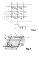
figure 2 représente le schéma électrique correspondant, où l'on voit pour chaque pixel un transistor Q, la capacité Ccl du cristal liquide de ce pixel, la capacité de stockage auxiliaire Cs, celle-ci étant reliée entre l'électrode du pixel (elle-même reliée à la source du transistor Q correspondant) et le conducteur de commande de la ligne suivante Li+1 ; la perte de tension aux bornes du cristal liquide au moment de la fin de l'impulsion (front descendant) de mise en conduction du transistor de commande est compensée par une augmentation de tension correspondante au moment du début (front montant) de l'impulsion de mise en conduction des transistors de la ligne suivante ; cette compensation est efficace si la valeur de la capacité de stockage auxiliaire est égale à la valeur de la capacité grille-source du transistor de commande ; - connecter la capacité de stockage auxiliaire, ou une capacité de compensation supplémentaire, à un conducteur de ligne auxiliaire, commun à tous les pixels de la ligne, fournissant une impulsion de compensation, d'amplitude ajustable, synchronisée avec l'impulsion de commande d'écriture et de sens contraire de celle-ci ; ainsi, lorsque le front descendant de l'impulsion de commande d'écriture tend à provoquer une diminution de tension sur l'électrode de pixel, le front montant de l'impulsion de compensation tend à provoquer une augmentation de cette tension, en proportion de l'amplitude de l'impulsion de compensation ; en ajustant le niveau d'amplitude de l'impulsion de compensation on peut compenser l'influence de la fin de l'impulsion de commande d'écriture ; la
figure 3 fait apparaître que chaque pixel est alors commandé par deux conducteurs de ligne, respectivement Li et L'i pour la ligne de rang i ; le deuxième conducteur de ligne L'i est relié à la deuxième borne de la capacité de stockage Cs, la première borne étant reliée à l'électrode de pixel du cristal liquide et à la source du transistor Q ; tous les pixels de la ligne sont connectés de cette manière au conducteur L'i ; alternativement on peut prévoir qu'il y a à la fois une capacité de stockage auxiliaire Cst simplement en parallèle avec le cristal liquide et une capacité de compensation Ccomp ; la capacité de compensation est alors reliée entre l'électrode de pixel et le conducteur de ligne L'i. Ces deux solutions sont représentées sur lafigure 3 . - Dans tous les cas, on a donc besoin de prévoir au moins une capacité (capacité de stockage auxiliaire et/ou capacité de compensation) dans le pixel.
- Dans les technologies d'afficheurs à matrice active sur panneaux de verre, dans lesquelles les transistors sont en silicium amorphe, on réalise le plus souvent le pixel avec une configuration telle que celle qui est représentée à la
figure 4 . Le pixel est rectangulaire ou carré et occupe une surface entre deux conducteurs de ligne successifs Li et Li+1 et deux conducteurs de colonne successifs Cj et Cj+1. L'électrode de pixel Ep, transparente, occupe la majeure partie de ce rectangle, et un coin du rectangle est occupé par le transistor Q en silicium amorphe dont la grille est reliée au conducteur de ligne Li, la source est reliée à l'électrode Ep, et le drain est relié au conducteur de colonne Cj. - La capacité de stockage auxiliaire Cs est dans ce cas tout simplement constituée par une extension latérale de l'électrode de pixel Ep et par le conducteur de ligne suivant Li+1 qui passe au-dessus de cette extension et qui en est séparé par une couche isolante. C'est la configuration de la
figure 2 adaptée à la technologie du silicium amorphe. L'électrode de pixel est en oxyde d'indium étain (ITO) qui a la propriété d'être transparent. - Ce type de structure de pixel est utilisable dans des afficheurs de type transmissif à matrice de transistors en silicium amorphe.
- Les afficheurs de petite dimension réalisés en technologie LCOS, c'est-à-dire sur substrat de silicium monocristallin, sont en général de type réflectif, de sorte que l'électrode Ep du pixel n'est pas transparente mais réfléchissante. Cette électrode n'est pas disposée latéralement à côté du transistor de commande Q comme pour les afficheurs en silicium amorphe tel que celui de la
figure 4 , mais elle recouvre complètement le transistor ; le transistor est naturellement protégé de la lumière par l'électrode du pixel. - Si on veut faire un afficheur en technologie LCOS qui soit de type transmissif, l'électrode du pixel ne peut plus être en métal réfléchissant car elle empêcherait le passage de la lumière : dans un afficheur transmissif la lumière issue d'une source de lumière traverse une seule fois le cristal liquide et les couches de circuits électroniques servant à commander les pixels, avant d'être observée ou projetée sur un écran, alors que dans un afficheur réflectif, elle traverse une première fois le cristal liquide, elle se réfléchit sur une électrode réfléchissante, et elle retraverse le cristal liquide.
- Dans un afficheur transmissif, il faut donc que l'électrode de pixel soit transparente (en ITO). Mais alors le transistor est exposé à la lumière, ce qui engendre des risques de fuites importantes et variables en fonction de l'éclairement du pixel. Ces fuites empêchent un maintien capacitif correct de la tension appliquée au pixel lors de l'écriture, alors que cette tension devrait subsister pendant tout le temps d'une trame suivant l'instant d'écriture.
- Par ailleurs, dans un afficheur en technologie LCOS sur un substrat de silicium monocristallin, les dimensions des pixels sont très petites ce qui rend difficile la mise en place de capacités de valeur suffisante dans chaque pixel.
- C'est pourquoi on propose selon l'invention un afficheur à cristal liquide de type transmissif comprenant une matrice de lignes et colonnes de pixels, chaque pixel comprenant un cristal liquide entre une électrode de pixel transparente et une contre-électrode transparente commune à tous les pixels, un transistor de commande et une capacité de stockage auxiliaire, la grille du transistor étant reliée à un premier conducteur de ligne commun à tous les pixels d'une même ligne pour recevoir de ce conducteur une impulsion de commande d'écriture, le drain du transistor étant relié à un conducteur de colonne commun à tous les pixels d'une même colonne pour en recevoir une tension analogique représentant un niveau de gris à afficher, et la source du transistor étant reliée à l'électrode du pixel et à une borne de la capacité de stockage auxiliaire, caractérisé en ce que le transistor est situé entre le cristal liquide et la capacité de stockage auxiliaire, la capacité étant réalisée par un empilement d'au moins deux structures en métal opaque à armatures interdigitées mises en parallèle, chaque structure étant réalisée dans un niveau de métallisation respectif, et les structures à armatures interdigitées comprenant des doigts parallèles dans chaque structure, les doigts d'une structure étant perpendiculaires aux doigts de l'autre structure.
- La capacité est alors située du côté amont (dans le sens de l'éclairement) de l'empilement constitué par le cristal liquide, le transistor de commande et la capacité de stockage auxiliaire. En utilisation, la source de lumière de l'afficheur éclaire donc la capacité mais ne peut pas ou presque pas éclairer le transistor. Celui-ci est masqué par la capacité. Le reste du pixel n'est pas masqué par la capacité et la lumière peut atteindre le cristal liquide (à travers l'électrode transparente) là où la capacité n'y fait pas obstacle.
- Le transistor et la capacité de stockage auxiliaire occupent une petite partie (inférieure à 50% et la plus faible possible) de la surface du pixel. L'encombrement latéral de la capacité doit en effet être minimisé pour que l'ouverture du pixel, c'est-à-dire le rapport entre la surface de pixel qui laisse passer la lumière et la surface totale du pixel reste aussi élevée que possible.
- Pour obtenir une capacité de stockage auxiliaire aussi élevée que possible dans un encombrement latéral aussi faible que possible, la capacité est réalisée par un empilement d'au moins deux structures à armatures interdigitées, chaque structure étant réalisée dans un niveau de métallisation opaque respectif. Les métallisations sont de préférence en aluminium et/ou en cuivre. Les structures interdigitées sont séparées par des couches isolantes et sont reliées entre elles par des vias conducteurs.
- Par exemple, dans un afficheur à six niveaux de métallisation, on peut prévoir que quatre niveaux superposés servent à réaliser quatre structures à armatures interdigitées ayant chacun deux armatures ; les armatures correspondantes des différents niveaux sont toutes reliées entre elles par des vias. Les directions des doigts de deux structures interdigitées de deux niveaux différents sont alternées (perpendiculaires entre elles) pour mieux masquer la lumière.
- Dans une réalisation, la capacité comporte une armature qui occupe une surface continue opaque recouvrant la totalité du transistor.
- Une capacité de compensation peut par ailleurs être réalisée dans le même empilement de couches métalliques que la capacité de stockage auxiliaire. Cette capacité est reliée électriquement entre l'électrode de pixel et une ligne conductrice permettant d'appliquer une tension de compensation. Cette capacité contribue à la protection du transistor contre la lumière et elle peut avoir une armature continue opaque recouvrant la totalité du transistor.
- Le transistor et la capacité de stockage auxiliaire sont de préférence réalisés sur la couche superficielle monocristalline d'un substrat de silicium sur isolant (SOI).
- D'autres caractéristiques et avantages de l'invention apparaîtront à la lecture de la description détaillée qui suit et qui est faite en référence aux dessins annexés dans lesquels :
- la
figure 1 représente la structure d'un afficheur matriciel à cristaux liquides ; - la
figure 2 représente un schéma électrique équivalent avec une capacité de stockage auxiliaire dans chaque pixel, raccordée à la ligne suivante ; - la
figure 3 représente un autre schéma avec une capacité de stockage auxiliaire, raccordée à un conducteur de ligne auxiliaire, avec éventuellement une capacité de compensation raccordée à un conducteur de commande ; - la
figure 4 représente un exemple de structure classique de pixel d'un afficheur à matrice active en silicium amorphe ; - la
figure 5 représente le schéma en coupe d'une structure de pixel selon l'invention en technologie LCOS de type transmissif ; - la
figure 6 représente schématiquement deux structures capacitives interdigitées ayant des doigts orientés selon des directions croisées, utilisables dans l'invention ; - la
figure 7 représente un schéma en coupe d'une autre structure de pixel, utilisant trois niveaux de métallisation ; - la
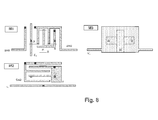
figure 8 représente en vue de dessus un exemple de motif de gravure de la métallisation pour chacun des trois niveaux de lafigure 7 . - L'afficheur à cristal liquide de type transmissif comprend une matrice de lignes et colonnes de pixels organisée par exemple comme sur l'un des schémas décrits aux
figures 1 à 3 ; seul un pixel est représenté sur la coupe de lafigure 5 ; chaque pixel comprend une cellule de cristal liquide CL entre une électrode de pixel Ep et une contre-électrode CE commune à tous les pixels ; le transistor de commande Q est réalisé dans une structure 10 de technologie CMOS, à base de silicium monocristallin, accolée à la cellule de cristal liquide. L'électrode commune CE et l'électrode de pixel Ep sont transparentes (en ITO), mais un bouclier opaque BCL (en aluminium par exemple) est localement interposé entre l'électrode de pixel et le transistor, pour protéger le transistor contre la lumière qui pourrait arriver par la cellule de cristal liquide par des phénomènes de réflexion. - Différentes technologies de fabrication existent pour la structure CMOS 10. Dans la technologie représentée à titre d'exemple, la structure 10 est formée à partir d'un substrat de silicium dit SOI (Silicon on Insulator, pour "silicium sur isolant") ; ce substrat comprend une superposition d'une couche isolante 12 d'oxyde de silicium adjacente à l'électrode de pixel Ep, et d'une couche de silicium monocristallin 14 dans laquelle est formé le transistor de commande. Le transistor représenté est un transistor NMOS comprenant une source et un drain dopés de type N+, séparés par un canal de type P recouvert par une grille isolée G, en silicium polycristallin ; le transistor pourrait alternativement être un transistor PMOS. Le transistor est séparé des transistors des pixels adjacents par de l'oxyde de silicium en tranchées isolantes superficielle (STI pour "shallow trench insulation").
- Le transistor est recouvert par une alternance de couches isolantes et métalliques permettant de former les interconnexions nécessaires pour établir le schéma électrique de la matrice de pixels, et permettant de former la capacité de stockage auxiliaire Cst et éventuellement la capacité de compensation Ccomp. Les couches métalliques sont reliées les unes aux autres et reliées au transistor par des vias conducteurs à travers les couches isolantes. Un via conducteur 16 formé dans la couche isolante 12 permet par ailleurs d'établir une connexion entre la source du transistor et l'électrode de pixel Ep.
- Les couches métalliques sont de préférence en aluminium et/ou en cuivre. Elles sont opaques à la lumière, et plus particulièrement opaques à la lumière d'une source lumineuse (non représentée) de l'afficheur, placée au-dessus de l'empilement représenté.
- Le transistor occupe une faible partie de la surface du pixel (de la même manière qu'on voyait un transistor occupant une faible partie de la surface du pixel dans la technologie en silicium amorphe de la
figure 4 ), et c'est cette partie du pixel qui est principalement représentée sur lafigure 5 . - Dans l'exemple représenté sur la
figure 5 , il y a six niveaux de métallisation superposés, désignés respectivement par les références M1 à M6. Le nombre de niveaux pourrait être différent. L'attribution des fonctions des différents niveaux peut varier et on en donnera simplement un exemple, mais dans tous les cas ils servent à réaliser la capacité de stockage Cst et éventuellement la capacité de compensation Ccomp; ils forment par ailleurs toutes les interconnexions internes au pixel et les interconnexions (lignes de commande, lignes de masse, conducteurs de colonnes, etc. nécessaire au fonctionnement de la matrice. Les niveaux métalliques sont représentés symboliquement par des traits horizontaux épais, et les vias sont représentés symboliquement par des traits verticaux épais ; les couches isolantes (en oxyde de silicium) qui séparent les niveaux sont déposées successivement entre les niveaux métalliques successivement déposés mais elles sont représentées comme une seule couche isolante 20 dans laquelle sont noyés les niveaux métalliques. - Dans l'exemple de la
figure 5 : - le niveau M1 sert à deux fonctions : réaliser le conducteur de ligne Li, relié par un via à la grille du transistor, et en même temps réaliser une connexion entre la source du transistor et l'électrode de pixel en utilisant le via 16 ;
- le niveau M2 sert à réaliser le conducteur de colonne C1 auquel est relié le pixel, relié par un via au drain du transistor, et en même temps à réaliser une partie de la capacité de stockage auxiliaire Cst ;
- le niveau M3 sert à réaliser une connexion vers une masse commune à toute la matrice, et en même temps à réaliser une autre partie de la capacité de stockage auxiliaire Cst ;
- les niveaux M4 et M5 servent à réaliser encore une partie de la capacité de stockage auxiliaire Cst ;
- et enfin, le niveau M6 sert à réaliser dans cet exemple une armature de la capacité de compensation Ccomp si la capacité de compensation est différente de la capacité de stockage, ou alors encore une partie de la capacité de stockage auxiliaire Cst s'il n'y a pas de capacité de compensation ; le niveau M6 sert aussi à constituer le conducteur de ligne de compensation L'i si le schéma est celui de la
figure 3 ; l'armature de capacité réalisée dans le dernier niveau M6 de l'empilement est de préférence une surface métallique (opaque) continue recouvrant l'ensemble des portions métalliques qui servent à réaliser la capacité de stockage Cst. - La répartition des conducteurs dans les différents niveaux métalliques peut être différente de celle qui a été indiquée ci-dessus : le niveau M1 plutôt que le niveau M3 peut servir par exemple à réaliser des lignes de connexion reliées à la masse ; le niveau M3 peut servir à réaliser la connexion L'i pour la capacité de compensation et la capacité de compensation elle-même s'il y en a une ; etc.
- La capacité de stockage auxiliaire Cst recouvre entièrement le transistor et empêche en grande partie la lumière de pénétrer jusqu'à lui ; le barrage contre la lumière est d'autant meilleur qu'il y a un plus grand nombre de niveaux métalliques au-dessus du transistor. Le bouclier opaque BCL protège également le transistor de la lumière susceptible d'arriver par-dessous.
- Pour maximiser la valeur de la capacité de stockage tout en limitant son encombrement latéral, on prévoit de préférence qu'elle est réalisée à partir d'une structure à armatures interdigitées, et on prévoit de préférence qu'elle est réalisée à partir de la surperposition de plusieurs structures à armatures interdigitées connectées électriquement en parallèle.
- Chacun des niveaux M2 à M5, dans le cas représenté à titre d'exemple, comporte une capacité partielle à armatures interdigitées, c'est-à-dire que les deux armatures de la capacité partielle sont formées dans un même niveau métallique. Chaque armature comprend une série de conducteurs (ou doigts de la structure) reliés électriquement entre eux, géographiquement proches des conducteurs d'une autre série de conducteurs appartenant à l'autre armature. La couche isolante 20 dans laquelle sont noyés les niveaux métalliques constitue le diélectrique entre les doigts appartenant à deux armatures. Le dessin entouré d'un cercle tireté est une vue de principe en plan de l'allure générale d'une telle capacité partielle dans le niveau M4 ; les autres niveaux sont réalisés de manière similaire. Le dessin représente des doigts parallèles pour les deux armatures, mais en pratique le dessin précis des armatures dépend de la place disponible dans chaque niveau compte-tenu des interconnexions à réaliser, et notamment compte-tenu des contraintes liées aux vias de contact à réaliser entre les niveaux de métallisation.
- Des vias conducteurs tels que 22 et 24 connectent les armatures correspondantes entre les différents niveaux, de sorte que la superposition des niveaux forme des capacités partielles en parallèle.
- Les doigts des armatures interdigitées sont orientés de préférence de manière croisée d'un niveau à l'autre, pour mieux empêcher la lumière de passer. La
figure 6 montre cette orientation croisée, dans une configuration simpliste où les doigts sont tous parallèles et rectilignes. Dans la réalité, les doigts des armatures des capacités peuvent avoir des formes plus tordues. - On ajoutera que si les peignes correspondant à deux niveaux non adjacents (tels que M3 et M5 par exemple) ont des doigts parallèles, on peut encore essayer de placer les doigts de l'un regard des intervalles entre doigts de l'autre, encore dans le but de limiter la pénétration de lumière.
- On comprendra que la capacité formée par des structures interdigitées peut être plus élevée que la capacité entre deux couches métalliques successives séparées par une couche isolante. En effet, la capacité résulte de la mise en regard sur toute leur longueur des doigts des structures. Les doigts sont allongés, ils peuvent être nombreux, et leur largeur et leur espacement peuvent être de quelques micromètres.
- Enfin, les vias conducteurs entre les différents niveaux de métallisation contribuent à la protection du transistor contre la lumière : ils tendent à piéger la lumière qui se propage latéralement , on aura donc avantage à prévoir plusieurs vias plutôt qu'un seul pour connecter deux éléments conducteurs qui doivent être reliés électriquement.
- Dans l'exemple de la
figure 5 , la capacité de compensation comprend une armature continue opaque, mais on comprendra qu'on peut prévoir alternativement que c'est la capacité de stockage Cst (ou les deux capacités) qui possède une armature continue opaque. - La
figure 7 représente un autre exemple de structure de pixel. Dans cet exemple on n'utilise que trois niveaux de métallisation M1, M2 et M3 ; on peut avoir intérêt en effet, pour des raisons de coût de fabrication, à minimiser le nombre de niveaux de métallisation ; l'efficacité de la protection contre la lumière diminue cependant ; en pratique il y aura au moins trois niveaux de métallisation et l'exemple de lafigure 7 comprend : - le niveau M1 sert à réaliser une connexion entre la source du transistor et l'électrode de pixel en utilisant le via 16 ; il sert aussi à réaliser le conducteur de colonne C1 auquel est relié le pixel, relié par un via au drain du transistor ; il sert à réaliser un conducteur de masse GND ; et enfin, il peut servir à former une capacité interdigitée qui constitue une partie de la capacité de stockage Cst ;
- le niveau M2 sert à réaliser le conducteur de ligne Li et une autre partie (interdigitée) de la capacité de stockage Cst, connectée en parallèle avec la partie de capacité formée dans le niveau M1 ;
- et enfin, le niveau M3 sert à réaliser dans cet exemple une armature de la capacité de compensation Ccomp si la capacité de compensation est différente de la capacité de stockage, ou alors encore une partie de la capacité de stockage auxiliaire Cst s'il n'y a pas de capacité de compensation ; le niveau M3 sert aussi à constituer le conducteur de ligne de compensation L'i si le schéma est celui de la
figure 3 ; l'armature de capacité réalisée dans le dernier niveau M3 de l'empilement est de préférence une surface métallique (opaque) continue recouvrant l'ensemble des portions métalliques qui servent à réaliser la capacité de stockage Cst ; l'autre armature de la capacité Ccomp est constituée par une des armatures de la capacité de stockage interdigitée du niveau M2. - La
figure 8 représente une configuration possible des trois niveaux métalliques M1, M2, M3 pour former les éléments indiqués ci-dessus. On y voit les vias de connexion entre les niveaux, représentés par des zones hachurées plus denses, ainsi que les vias de connexion avec la source, la grille et le drain du transistor. - La capacité de stockage auxiliaire Cst recouvre le transistor et empêche en grande partie la lumière de pénétrer jusqu'à lui ; le barrage contre la lumière est d'autant meilleur qu'il y a un plus grand nombre de niveaux métalliques au-dessus du transistor.
- Dans la configuration de la
figure 8 , c'est la capacité de compensation Ccomp qui possède une armature continue opaque recouvrant la totalité du transistor pour mieux le protéger de la lumière. L'ensemble de la capacité de stockage et de la capacité de compensation offrent donc une très bonne protection du transistor contre un éclairement par la source de lumière de l'afficheur transmissif.
Claims (7)
- Afficheur à cristal liquide de type transmissif comprenant une matrice de lignes et colonnes de pixels, chaque pixel comprenant un cristal liquide CL entre une électrode de pixel (EP) transparente et une contre-électrode (CE) transparente commune à tous les pixels, un transistor de commande (Q) et une capacité de stockage auxiliaire (Cs), la grille du transistor étant reliée à un premier conducteur de ligne (Li) commun à tous les pixels d'une même ligne pour recevoir de ce conducteur une impulsion de commande d'écriture, le drain du transistor étant relié à un conducteur de colonne (C1) commun à tous les pixels d'une même colonne pour en recevoir une tension analogique représentant un niveau de gris à afficher, et la source du transistor étant reliée à l'électrode du pixel et à une borne de la capacité de stockage auxiliaire, caractérisé en ce que le transistor est situé entre le cristal liquide et la capacité de stockage auxiliaire, la capacité étant réalisée par un empilement d'au moins deux structures en métal opaque à armatures interdigitées mises en parallèle, chaque structure étant réalisée dans un niveau de métallisation respectif (M2 à M5), et les structures à armatures interdigitées comprenant des doigts parallèles dans chaque structure, les doigts d'une structure étant perpendiculaires aux doigts de l'autre structure.
- Afficheur selon la revendication 1, caractérisé en ce que le transistor et la capacité de stockage auxiliaire occupent une surface inférieure à 50% de la surface du pixel.
- Afficheur selon la revendication 2, caractérisé en ce que la capacité est réalisée dans un empilement d'au moins trois niveaux de métallisation séparés par des couches isolantes, avec des vias conducteurs (22, 24) pour relier entre eux les différents niveaux en fonction des interconnexions à établir.
- Afficheur selon l'une des revendications 1 à 3, caractérisé en ce que la capacité comporte une armature constituant une surface continue opaque recouvrant la totalité du transistor.
- Afficheur selon l'une des revendications 1 à 5, caractérisé en ce qu'il comporte une capacité de compensation Ccomp reliée à un conducteur de ligne auxiliaire (L'i) reliant tous les pixels de la même ligne, la capacité de compensation étant située au-dessus du transistor.
- Afficheur selon la revendication 5, caractérisé en ce que la capacité de compensation comporte une armature avec une surface continue opaque recouvrant la totalité du transistor.
- Afficheur selon l'une des revendications 1 à 6, caractérisé en ce qu'il est réalisé en technologie LCOS, le transistor et la capacité de stockage auxiliaire étant réalisés sur la couche superficielle monocristalline d'un substrat de silicium monocristallin sur isolant (SOI).
Applications Claiming Priority (1)
| Application Number | Priority Date | Filing Date | Title |
|---|---|---|---|
| FR1003996A FR2965942B1 (fr) | 2010-10-08 | 2010-10-08 | Afficheur a cristal liquide de type transmissif en technologie cmos avec capacite de stockage auxiliaire |
Publications (2)
| Publication Number | Publication Date |
|---|---|
| EP2439583A1 true EP2439583A1 (fr) | 2012-04-11 |
| EP2439583B1 EP2439583B1 (fr) | 2015-04-08 |
Family
ID=43428593
Family Applications (1)
| Application Number | Title | Priority Date | Filing Date |
|---|---|---|---|
| EP11183971.8A Not-in-force EP2439583B1 (fr) | 2010-10-08 | 2011-10-05 | Afficheur a cristal liquide de type transmissif en technologie CMOS avec capacité de stockage auxiliaire |
Country Status (4)
| Country | Link |
|---|---|
| US (1) | US20120086683A1 (fr) |
| EP (1) | EP2439583B1 (fr) |
| JP (1) | JP5906551B2 (fr) |
| FR (1) | FR2965942B1 (fr) |
Cited By (2)
| Publication number | Priority date | Publication date | Assignee | Title |
|---|---|---|---|---|
| EP2677361A1 (fr) * | 2012-06-19 | 2013-12-25 | STmicroelectronics SA | Panneau constitué d'une matrice de cellules à cristaux liquides destiné à être utilisé dans un nanoprojecteur |
| FR2996682A1 (fr) * | 2012-10-10 | 2014-04-11 | Commissariat Energie Atomique | Procede ameliore d'interconnexion pour micro-imageur |
Families Citing this family (10)
| Publication number | Priority date | Publication date | Assignee | Title |
|---|---|---|---|---|
| JP2014102319A (ja) * | 2012-11-19 | 2014-06-05 | Sony Corp | 発光素子及び表示装置 |
| KR102032382B1 (ko) * | 2013-01-31 | 2019-10-16 | 삼성디스플레이 주식회사 | 표시장치의 커패시터 제조 방법 및 그에 따라 제조된 커패시터를 구비하는 표시장치 |
| CN104716157B (zh) * | 2013-12-16 | 2018-04-17 | 昆山工研院新型平板显示技术中心有限公司 | 一种有机发光显示装置的阵列基板及其制备方法 |
| US10734330B2 (en) * | 2015-01-30 | 2020-08-04 | Taiwan Semiconductor Manufacturing Company Limited | Semiconductor devices having an electro-static discharge protection structure |
| JP6365368B2 (ja) * | 2015-03-19 | 2018-08-01 | 株式会社Jvcケンウッド | 液晶表示装置 |
| JP6380186B2 (ja) * | 2015-03-25 | 2018-08-29 | 株式会社Jvcケンウッド | 液晶表示装置 |
| US20160343796A1 (en) * | 2015-05-22 | 2016-11-24 | Mediatek Inc. | Capacitor structure and method for forming the same |
| JP6717071B2 (ja) * | 2016-06-15 | 2020-07-01 | セイコーエプソン株式会社 | キャパシター回路、回路装置、物理量検出装置、電子機器及び移動体 |
| FR3063387B1 (fr) * | 2017-02-24 | 2021-05-21 | Commissariat Energie Atomique | Composant electronique muni d'un transistor et de doigts interdigites pour former au moins une partie d'un composant capacitif au sein du composant electronique |
| US11538748B2 (en) * | 2020-06-04 | 2022-12-27 | Mediatek Singapore Pte. Ltd. | Semiconductor device with capacitor element |
Citations (7)
| Publication number | Priority date | Publication date | Assignee | Title |
|---|---|---|---|---|
| WO2001007961A1 (fr) * | 1999-07-21 | 2001-02-01 | E Ink Corporation | Utilisation d'un condensateur de memorisation pour ameliorer la performance d'un affichage electronique matriciel actif |
| JP2003297930A (ja) * | 2002-03-29 | 2003-10-17 | Gurinikusu:Kk | 櫛型キャパシタ |
| US20040119899A1 (en) * | 2002-11-26 | 2004-06-24 | Seiko Epson Corporation | Wiring structure, method for manufacturing the same, electro-optical device, and electronic device |
| US20040257489A1 (en) * | 2002-10-31 | 2004-12-23 | Sharp Kabushiki Kaisha | Active matrix substrate and display device |
| US20060024905A1 (en) * | 2004-07-30 | 2006-02-02 | Canzhong He | Metal capacitor stacked with a MOS capacitor to provide increased capacitance density |
| US20070181918A1 (en) * | 2006-02-03 | 2007-08-09 | Kabushiki Kaisha Toshiba | Semiconductor device |
| JP2009135149A (ja) * | 2007-11-28 | 2009-06-18 | Panasonic Corp | 半導体集積回路 |
Family Cites Families (7)
| Publication number | Priority date | Publication date | Assignee | Title |
|---|---|---|---|---|
| JP3522144B2 (ja) * | 1999-02-25 | 2004-04-26 | 富士通株式会社 | 容量回路および半導体集積回路装置 |
| US6677613B1 (en) * | 1999-03-03 | 2004-01-13 | Semiconductor Energy Laboratory Co., Ltd. | Semiconductor device and method of fabricating the same |
| JP4907003B2 (ja) * | 1999-12-27 | 2012-03-28 | 株式会社半導体エネルギー研究所 | アクティブマトリクス型表示装置およびそれを用いた電気器具 |
| CN1267782C (zh) * | 2000-04-21 | 2006-08-02 | 精工爱普生株式会社 | 电光装置 |
| US7741670B2 (en) * | 2005-09-30 | 2010-06-22 | Broadcom Corporation | Semiconductor decoupling capacitor |
| US8022458B2 (en) * | 2007-10-08 | 2011-09-20 | Taiwan Semiconductor Manufacturing Company, Ltd. | Capacitors integrated with metal gate formation |
| US8138539B2 (en) * | 2007-11-29 | 2012-03-20 | Infineon Technologies Ag | Semiconductor devices and methods of manufacture thereof |
-
2010
- 2010-10-08 FR FR1003996A patent/FR2965942B1/fr not_active Expired - Fee Related
-
2011
- 2011-10-05 EP EP11183971.8A patent/EP2439583B1/fr not_active Not-in-force
- 2011-10-05 JP JP2011221369A patent/JP5906551B2/ja not_active Expired - Fee Related
- 2011-10-07 US US13/268,182 patent/US20120086683A1/en not_active Abandoned
Patent Citations (7)
| Publication number | Priority date | Publication date | Assignee | Title |
|---|---|---|---|---|
| WO2001007961A1 (fr) * | 1999-07-21 | 2001-02-01 | E Ink Corporation | Utilisation d'un condensateur de memorisation pour ameliorer la performance d'un affichage electronique matriciel actif |
| JP2003297930A (ja) * | 2002-03-29 | 2003-10-17 | Gurinikusu:Kk | 櫛型キャパシタ |
| US20040257489A1 (en) * | 2002-10-31 | 2004-12-23 | Sharp Kabushiki Kaisha | Active matrix substrate and display device |
| US20040119899A1 (en) * | 2002-11-26 | 2004-06-24 | Seiko Epson Corporation | Wiring structure, method for manufacturing the same, electro-optical device, and electronic device |
| US20060024905A1 (en) * | 2004-07-30 | 2006-02-02 | Canzhong He | Metal capacitor stacked with a MOS capacitor to provide increased capacitance density |
| US20070181918A1 (en) * | 2006-02-03 | 2007-08-09 | Kabushiki Kaisha Toshiba | Semiconductor device |
| JP2009135149A (ja) * | 2007-11-28 | 2009-06-18 | Panasonic Corp | 半導体集積回路 |
Cited By (4)
| Publication number | Priority date | Publication date | Assignee | Title |
|---|---|---|---|---|
| EP2677361A1 (fr) * | 2012-06-19 | 2013-12-25 | STmicroelectronics SA | Panneau constitué d'une matrice de cellules à cristaux liquides destiné à être utilisé dans un nanoprojecteur |
| FR2996682A1 (fr) * | 2012-10-10 | 2014-04-11 | Commissariat Energie Atomique | Procede ameliore d'interconnexion pour micro-imageur |
| EP2720083A1 (fr) * | 2012-10-10 | 2014-04-16 | Commissariat A L'energie Atomique Et Aux Energies Alternatives | Procédé amélioré d'interconnexion pour micro-imageur |
| US8945977B2 (en) | 2012-10-10 | 2015-02-03 | Commissariat A L'energie Atomique Et Aux Energies Alternatives | Interconnection method for a micro-imaging device |
Also Published As
| Publication number | Publication date |
|---|---|
| US20120086683A1 (en) | 2012-04-12 |
| FR2965942A1 (fr) | 2012-04-13 |
| FR2965942B1 (fr) | 2013-02-22 |
| JP5906551B2 (ja) | 2016-04-20 |
| EP2439583B1 (fr) | 2015-04-08 |
| JP2012083754A (ja) | 2012-04-26 |
Similar Documents
| Publication | Publication Date | Title |
|---|---|---|
| EP2439583B1 (fr) | Afficheur a cristal liquide de type transmissif en technologie CMOS avec capacité de stockage auxiliaire | |
| FR2585167A1 (fr) | Structures conductrices redondantes pour affichages a cristaux liquides commandes par des transistors a effet de champ en couche mince | |
| JP4483235B2 (ja) | トランジスタアレイ基板の製造方法及びトランジスタアレイ基板 | |
| EP0289415B1 (fr) | Ecran matriciel d'affichage à cristaux liquides muni de capacités de stockage | |
| EP0145520B1 (fr) | Ecran d'affichage à matrice active sans croisement des lignes et des colonnes d'adressage | |
| FR2702286A1 (fr) | Affichage à cristaux liquides et procédé pour le fabriquer. | |
| FR2973921A1 (fr) | Module tactile double mode et ecran tactile double mode | |
| FR2649234A1 (fr) | Dispositif de visualisation a cristal liquide avec des transistors a effet de champs redondants et des croisements redondants connectes par des liaisons fusibles par laser | |
| CN105629612A (zh) | 薄膜晶体管阵列基板及其制作方法 | |
| EP2721598B1 (fr) | Afficheur a cristal liquide a electrodes d'effacement | |
| EP0689721A1 (fr) | Procede de fabrication de transistors a couches minces etages directs | |
| EP0506528B1 (fr) | Structure de commande matricielle pour écran de visualisation | |
| FR2599171A1 (fr) | Ecran de visualisation electrooptique et procede de realisation | |
| EP0564337B1 (fr) | Ecran d'affichage à masque optique et procédé de réalisation de cet écran | |
| EP0197992B1 (fr) | Ecran d'affichage a matrice active a double transistor d'adressage | |
| EP1567911B1 (fr) | Structure de matrice active pour ecran de visualisation et ecran comportant une telle matrice | |
| EP0256927B1 (fr) | Dispositif d'affichage matriciel comprenant deux paquets d'électrodes lignes et deux électrodes colonnes par élément image et son procédé de commande | |
| EP0607352B1 (fr) | Afficheur a matrice active utilisant un plan de masse enterre | |
| EP2677361B1 (fr) | Panneau constitué d'une matrice de cellules à cristaux liquides destiné à être utilisé dans un nanoprojecteur | |
| WO2007014953A1 (fr) | Matrice active pour un dispositif d'affichage a cristal liquide | |
| TW513589B (en) | Thin film transistor liquid crystal display with storage capacitor having light-blocking effect | |
| FR2532116A1 (fr) | Transistor a couche mince et dispositif d'affichage a cristaux liquides utilisant ce transistor | |
| FR2530868A1 (fr) | Transistor a couche mince et dispositif d'affichage a cristaux liquides utilisant ce transistor |
Legal Events
| Date | Code | Title | Description |
|---|---|---|---|
| AK | Designated contracting states |
Kind code of ref document: A1 Designated state(s): AL AT BE BG CH CY CZ DE DK EE ES FI FR GB GR HR HU IE IS IT LI LT LU LV MC MK MT NL NO PL PT RO RS SE SI SK SM TR |
|
| AX | Request for extension of the european patent |
Extension state: BA ME |
|
| PUAI | Public reference made under article 153(3) epc to a published international application that has entered the european phase |
Free format text: ORIGINAL CODE: 0009012 |
|
| 17P | Request for examination filed |
Effective date: 20121010 |
|
| GRAP | Despatch of communication of intention to grant a patent |
Free format text: ORIGINAL CODE: EPIDOSNIGR1 |
|
| INTG | Intention to grant announced |
Effective date: 20141112 |
|
| GRAS | Grant fee paid |
Free format text: ORIGINAL CODE: EPIDOSNIGR3 |
|
| GRAA | (expected) grant |
Free format text: ORIGINAL CODE: 0009210 |
|
| AK | Designated contracting states |
Kind code of ref document: B1 Designated state(s): AL AT BE BG CH CY CZ DE DK EE ES FI FR GB GR HR HU IE IS IT LI LT LU LV MC MK MT NL NO PL PT RO RS SE SI SK SM TR |
|
| REG | Reference to a national code |
Ref country code: GB Ref legal event code: FG4D Free format text: NOT ENGLISH |
|
| REG | Reference to a national code |
Ref country code: CH Ref legal event code: EP |
|
| REG | Reference to a national code |
Ref country code: IE Ref legal event code: FG4D Free format text: LANGUAGE OF EP DOCUMENT: FRENCH |
|
| REG | Reference to a national code |
Ref country code: AT Ref legal event code: REF Ref document number: 720996 Country of ref document: AT Kind code of ref document: T Effective date: 20150515 |
|
| REG | Reference to a national code |
Ref country code: DE Ref legal event code: R096 Ref document number: 602011015393 Country of ref document: DE Effective date: 20150521 |
|
| REG | Reference to a national code |
Ref country code: AT Ref legal event code: MK05 Ref document number: 720996 Country of ref document: AT Kind code of ref document: T Effective date: 20150408 |
|
| REG | Reference to a national code |
Ref country code: NL Ref legal event code: VDEP Effective date: 20150408 |
|
| REG | Reference to a national code |
Ref country code: LT Ref legal event code: MG4D |
|
| PG25 | Lapsed in a contracting state [announced via postgrant information from national office to epo] |
Ref country code: NL Free format text: LAPSE BECAUSE OF FAILURE TO SUBMIT A TRANSLATION OF THE DESCRIPTION OR TO PAY THE FEE WITHIN THE PRESCRIBED TIME-LIMIT Effective date: 20150408 |
|
| PG25 | Lapsed in a contracting state [announced via postgrant information from national office to epo] |
Ref country code: HR Free format text: LAPSE BECAUSE OF FAILURE TO SUBMIT A TRANSLATION OF THE DESCRIPTION OR TO PAY THE FEE WITHIN THE PRESCRIBED TIME-LIMIT Effective date: 20150408 Ref country code: NO Free format text: LAPSE BECAUSE OF FAILURE TO SUBMIT A TRANSLATION OF THE DESCRIPTION OR TO PAY THE FEE WITHIN THE PRESCRIBED TIME-LIMIT Effective date: 20150708 Ref country code: PT Free format text: LAPSE BECAUSE OF FAILURE TO SUBMIT A TRANSLATION OF THE DESCRIPTION OR TO PAY THE FEE WITHIN THE PRESCRIBED TIME-LIMIT Effective date: 20150810 Ref country code: LT Free format text: LAPSE BECAUSE OF FAILURE TO SUBMIT A TRANSLATION OF THE DESCRIPTION OR TO PAY THE FEE WITHIN THE PRESCRIBED TIME-LIMIT Effective date: 20150408 Ref country code: FI Free format text: LAPSE BECAUSE OF FAILURE TO SUBMIT A TRANSLATION OF THE DESCRIPTION OR TO PAY THE FEE WITHIN THE PRESCRIBED TIME-LIMIT Effective date: 20150408 Ref country code: ES Free format text: LAPSE BECAUSE OF FAILURE TO SUBMIT A TRANSLATION OF THE DESCRIPTION OR TO PAY THE FEE WITHIN THE PRESCRIBED TIME-LIMIT Effective date: 20150408 |
|
| REG | Reference to a national code |
Ref country code: FR Ref legal event code: PLFP Year of fee payment: 5 |
|
| PG25 | Lapsed in a contracting state [announced via postgrant information from national office to epo] |
Ref country code: IS Free format text: LAPSE BECAUSE OF FAILURE TO SUBMIT A TRANSLATION OF THE DESCRIPTION OR TO PAY THE FEE WITHIN THE PRESCRIBED TIME-LIMIT Effective date: 20150808 Ref country code: GR Free format text: LAPSE BECAUSE OF FAILURE TO SUBMIT A TRANSLATION OF THE DESCRIPTION OR TO PAY THE FEE WITHIN THE PRESCRIBED TIME-LIMIT Effective date: 20150709 Ref country code: RS Free format text: LAPSE BECAUSE OF FAILURE TO SUBMIT A TRANSLATION OF THE DESCRIPTION OR TO PAY THE FEE WITHIN THE PRESCRIBED TIME-LIMIT Effective date: 20150408 Ref country code: AT Free format text: LAPSE BECAUSE OF FAILURE TO SUBMIT A TRANSLATION OF THE DESCRIPTION OR TO PAY THE FEE WITHIN THE PRESCRIBED TIME-LIMIT Effective date: 20150408 Ref country code: LV Free format text: LAPSE BECAUSE OF FAILURE TO SUBMIT A TRANSLATION OF THE DESCRIPTION OR TO PAY THE FEE WITHIN THE PRESCRIBED TIME-LIMIT Effective date: 20150408 |
|
| REG | Reference to a national code |
Ref country code: DE Ref legal event code: R097 Ref document number: 602011015393 Country of ref document: DE |
|
| PG25 | Lapsed in a contracting state [announced via postgrant information from national office to epo] |
Ref country code: DK Free format text: LAPSE BECAUSE OF FAILURE TO SUBMIT A TRANSLATION OF THE DESCRIPTION OR TO PAY THE FEE WITHIN THE PRESCRIBED TIME-LIMIT Effective date: 20150408 Ref country code: EE Free format text: LAPSE BECAUSE OF FAILURE TO SUBMIT A TRANSLATION OF THE DESCRIPTION OR TO PAY THE FEE WITHIN THE PRESCRIBED TIME-LIMIT Effective date: 20150408 |
|
| PGFP | Annual fee paid to national office [announced via postgrant information from national office to epo] |
Ref country code: GB Payment date: 20151019 Year of fee payment: 5 Ref country code: DE Payment date: 20151014 Year of fee payment: 5 |
|
| PLBE | No opposition filed within time limit |
Free format text: ORIGINAL CODE: 0009261 |
|
| STAA | Information on the status of an ep patent application or granted ep patent |
Free format text: STATUS: NO OPPOSITION FILED WITHIN TIME LIMIT |
|
| PG25 | Lapsed in a contracting state [announced via postgrant information from national office to epo] |
Ref country code: CZ Free format text: LAPSE BECAUSE OF FAILURE TO SUBMIT A TRANSLATION OF THE DESCRIPTION OR TO PAY THE FEE WITHIN THE PRESCRIBED TIME-LIMIT Effective date: 20150408 Ref country code: PL Free format text: LAPSE BECAUSE OF FAILURE TO SUBMIT A TRANSLATION OF THE DESCRIPTION OR TO PAY THE FEE WITHIN THE PRESCRIBED TIME-LIMIT Effective date: 20150408 Ref country code: SK Free format text: LAPSE BECAUSE OF FAILURE TO SUBMIT A TRANSLATION OF THE DESCRIPTION OR TO PAY THE FEE WITHIN THE PRESCRIBED TIME-LIMIT Effective date: 20150408 Ref country code: RO Free format text: LAPSE BECAUSE OF NON-PAYMENT OF DUE FEES Effective date: 20150408 |
|
| PGFP | Annual fee paid to national office [announced via postgrant information from national office to epo] |
Ref country code: FR Payment date: 20151102 Year of fee payment: 5 |
|
| 26N | No opposition filed |
Effective date: 20160111 |
|
| PG25 | Lapsed in a contracting state [announced via postgrant information from national office to epo] |
Ref country code: IT Free format text: LAPSE BECAUSE OF FAILURE TO SUBMIT A TRANSLATION OF THE DESCRIPTION OR TO PAY THE FEE WITHIN THE PRESCRIBED TIME-LIMIT Effective date: 20150408 |
|
| PG25 | Lapsed in a contracting state [announced via postgrant information from national office to epo] |
Ref country code: SI Free format text: LAPSE BECAUSE OF FAILURE TO SUBMIT A TRANSLATION OF THE DESCRIPTION OR TO PAY THE FEE WITHIN THE PRESCRIBED TIME-LIMIT Effective date: 20150408 Ref country code: LU Free format text: LAPSE BECAUSE OF FAILURE TO SUBMIT A TRANSLATION OF THE DESCRIPTION OR TO PAY THE FEE WITHIN THE PRESCRIBED TIME-LIMIT Effective date: 20151005 |
|
| REG | Reference to a national code |
Ref country code: CH Ref legal event code: PL |
|
| PG25 | Lapsed in a contracting state [announced via postgrant information from national office to epo] |
Ref country code: MC Free format text: LAPSE BECAUSE OF FAILURE TO SUBMIT A TRANSLATION OF THE DESCRIPTION OR TO PAY THE FEE WITHIN THE PRESCRIBED TIME-LIMIT Effective date: 20150408 |
|
| REG | Reference to a national code |
Ref country code: IE Ref legal event code: MM4A |
|
| PG25 | Lapsed in a contracting state [announced via postgrant information from national office to epo] |
Ref country code: CH Free format text: LAPSE BECAUSE OF NON-PAYMENT OF DUE FEES Effective date: 20151031 Ref country code: LI Free format text: LAPSE BECAUSE OF NON-PAYMENT OF DUE FEES Effective date: 20151031 |
|
| PG25 | Lapsed in a contracting state [announced via postgrant information from national office to epo] |
Ref country code: IE Free format text: LAPSE BECAUSE OF NON-PAYMENT OF DUE FEES Effective date: 20151005 |
|
| REG | Reference to a national code |
Ref country code: DE Ref legal event code: R119 Ref document number: 602011015393 Country of ref document: DE |
|
| PG25 | Lapsed in a contracting state [announced via postgrant information from national office to epo] |
Ref country code: HU Free format text: LAPSE BECAUSE OF FAILURE TO SUBMIT A TRANSLATION OF THE DESCRIPTION OR TO PAY THE FEE WITHIN THE PRESCRIBED TIME-LIMIT; INVALID AB INITIO Effective date: 20111005 Ref country code: BG Free format text: LAPSE BECAUSE OF FAILURE TO SUBMIT A TRANSLATION OF THE DESCRIPTION OR TO PAY THE FEE WITHIN THE PRESCRIBED TIME-LIMIT Effective date: 20150408 Ref country code: SM Free format text: LAPSE BECAUSE OF FAILURE TO SUBMIT A TRANSLATION OF THE DESCRIPTION OR TO PAY THE FEE WITHIN THE PRESCRIBED TIME-LIMIT Effective date: 20150408 |
|
| GBPC | Gb: european patent ceased through non-payment of renewal fee |
Effective date: 20161005 |
|
| PG25 | Lapsed in a contracting state [announced via postgrant information from national office to epo] |
Ref country code: CY Free format text: LAPSE BECAUSE OF FAILURE TO SUBMIT A TRANSLATION OF THE DESCRIPTION OR TO PAY THE FEE WITHIN THE PRESCRIBED TIME-LIMIT Effective date: 20150408 Ref country code: SE Free format text: LAPSE BECAUSE OF FAILURE TO SUBMIT A TRANSLATION OF THE DESCRIPTION OR TO PAY THE FEE WITHIN THE PRESCRIBED TIME-LIMIT Effective date: 20150408 |
|
| REG | Reference to a national code |
Ref country code: FR Ref legal event code: ST Effective date: 20170630 |
|
| PG25 | Lapsed in a contracting state [announced via postgrant information from national office to epo] |
Ref country code: FR Free format text: LAPSE BECAUSE OF NON-PAYMENT OF DUE FEES Effective date: 20161102 Ref country code: GB Free format text: LAPSE BECAUSE OF NON-PAYMENT OF DUE FEES Effective date: 20161005 Ref country code: BE Free format text: LAPSE BECAUSE OF NON-PAYMENT OF DUE FEES Effective date: 20151031 Ref country code: DE Free format text: LAPSE BECAUSE OF NON-PAYMENT OF DUE FEES Effective date: 20170503 |
|
| PG25 | Lapsed in a contracting state [announced via postgrant information from national office to epo] |
Ref country code: MT Free format text: LAPSE BECAUSE OF FAILURE TO SUBMIT A TRANSLATION OF THE DESCRIPTION OR TO PAY THE FEE WITHIN THE PRESCRIBED TIME-LIMIT Effective date: 20150408 Ref country code: TR Free format text: LAPSE BECAUSE OF FAILURE TO SUBMIT A TRANSLATION OF THE DESCRIPTION OR TO PAY THE FEE WITHIN THE PRESCRIBED TIME-LIMIT Effective date: 20150408 |
|
| PG25 | Lapsed in a contracting state [announced via postgrant information from national office to epo] |
Ref country code: MK Free format text: LAPSE BECAUSE OF FAILURE TO SUBMIT A TRANSLATION OF THE DESCRIPTION OR TO PAY THE FEE WITHIN THE PRESCRIBED TIME-LIMIT Effective date: 20150408 |
|
| PG25 | Lapsed in a contracting state [announced via postgrant information from national office to epo] |
Ref country code: AL Free format text: LAPSE BECAUSE OF FAILURE TO SUBMIT A TRANSLATION OF THE DESCRIPTION OR TO PAY THE FEE WITHIN THE PRESCRIBED TIME-LIMIT Effective date: 20150408 |