EP2489048B1 - Integrierter transformator mit mehreren transformationsverhältnissen - Google Patents
Integrierter transformator mit mehreren transformationsverhältnissen Download PDFInfo
- Publication number
- EP2489048B1 EP2489048B1 EP10768722.0A EP10768722A EP2489048B1 EP 2489048 B1 EP2489048 B1 EP 2489048B1 EP 10768722 A EP10768722 A EP 10768722A EP 2489048 B1 EP2489048 B1 EP 2489048B1
- Authority
- EP
- European Patent Office
- Prior art keywords
- circuit
- primary
- circuits
- inductors
- radio frequency
- Prior art date
- Legal status (The legal status is an assumption and is not a legal conclusion. Google has not performed a legal analysis and makes no representation as to the accuracy of the status listed.)
- Not-in-force
Links
- 230000009466 transformation Effects 0.000 title claims description 11
- 238000004891 communication Methods 0.000 claims description 9
- 101100072620 Streptomyces griseus ind2 gene Proteins 0.000 claims description 6
- 102100032533 ADP/ATP translocase 1 Human genes 0.000 claims description 4
- 102100026396 ADP/ATP translocase 2 Human genes 0.000 claims description 4
- 101000768061 Escherichia phage P1 Antirepressor protein 1 Proteins 0.000 claims description 4
- 101000796932 Homo sapiens ADP/ATP translocase 1 Proteins 0.000 claims description 4
- 101000718417 Homo sapiens ADP/ATP translocase 2 Proteins 0.000 claims description 4
- 102100040792 DNA primase small subunit Human genes 0.000 description 13
- 101000611567 Homo sapiens DNA primase small subunit Proteins 0.000 description 13
- 102100040795 DNA primase large subunit Human genes 0.000 description 10
- 101000611553 Homo sapiens DNA primase large subunit Proteins 0.000 description 10
- 101001107782 Homo sapiens Iron-sulfur protein NUBPL Proteins 0.000 description 5
- 102100021998 Iron-sulfur protein NUBPL Human genes 0.000 description 5
- XUIMIQQOPSSXEZ-UHFFFAOYSA-N Silicon Chemical compound [Si] XUIMIQQOPSSXEZ-UHFFFAOYSA-N 0.000 description 3
- 229910052710 silicon Inorganic materials 0.000 description 3
- 239000010703 silicon Substances 0.000 description 3
- 101100072627 Arabidopsis thaliana IND gene Proteins 0.000 description 2
- 230000003321 amplification Effects 0.000 description 1
- 230000005540 biological transmission Effects 0.000 description 1
- 230000000295 complement effect Effects 0.000 description 1
- 230000008878 coupling Effects 0.000 description 1
- 238000010168 coupling process Methods 0.000 description 1
- 238000005859 coupling reaction Methods 0.000 description 1
- 238000005530 etching Methods 0.000 description 1
- 238000000034 method Methods 0.000 description 1
- 238000003199 nucleic acid amplification method Methods 0.000 description 1
- 238000000206 photolithography Methods 0.000 description 1
- 239000000758 substrate Substances 0.000 description 1
Images


Classifications
-
- H—ELECTRICITY
- H01—ELECTRIC ELEMENTS
- H01F—MAGNETS; INDUCTANCES; TRANSFORMERS; SELECTION OF MATERIALS FOR THEIR MAGNETIC PROPERTIES
- H01F19/00—Fixed transformers or mutual inductances of the signal type
- H01F19/04—Transformers or mutual inductances suitable for handling frequencies considerably beyond the audio range
-
- H—ELECTRICITY
- H03—ELECTRONIC CIRCUITRY
- H03H—IMPEDANCE NETWORKS, e.g. RESONANT CIRCUITS; RESONATORS
- H03H7/00—Multiple-port networks comprising only passive electrical elements as network components
- H03H7/38—Impedance-matching networks
Definitions
- This invention relates to the transformers used in integrated electronic components.
- RF radio frequency
- radio frequency transmitters and receivers use differential architectures. Antennas, as well as the power amplifiers associated with them, do not have this differential structure, however. A transformation of the differential signals from communication circuits should therefore be performed before they are delivered to the power amplification stage and the antenna (antenna stage, for short).
- the radio transmitters and receivers of today operate in different modes and on different frequency bands.
- transmitters and receivers currently have different outputs for various applications.
- some devices can operate in compliance with different standards, and therefore have different antenna stages (for example operating in WCDMA and in GSM/EDGE).
- Magnetic transformers are used to perform this transformation and also to match the output from these circuits to a particular antenna amplifier.
- transformers comprise inductors, and including these inductors in an integrated circuit requires a large silicon surface area.
- a matching circuit MATCH is positioned between two communication circuits CIRC1 and CIRC2 on the one hand and two antenna amplifiers AMPLI1 and AMPLI2 on the other hand.
- the antenna amplifiers APMLI1 and APMLI2 are respectively connected to the antennas ANT1, ANT2.
- the circuit MATCH comprises two transformers TRSFO1 and TRSFO2, respectively coupled to the circuits CIRC1 and CIRC2.
- the circuits CIRC1 and CIRC2 have a differential structure.
- the two outputs from each circuit are connected to the two terminals of the transformers' primary circuits.
- the transformers' secondary circuits have a terminal connected to the ground and a terminal connected to each of the amplifiers AMPLI1 and AMPLI2.
- a radio frequency circuit comprising a transformer with a first primary circuit, a second primary circuit, and a secondary circuit.
- the secondary circuit comprises a first integrated inductor which is positioned, on an axis orthogonal to a surface of the circuit, between a second integrated and a third inductors respectively comprised in the first primary circuit and second primary circuit.
- the present invention takes advantage of the large number of layers in integrated circuits as they are currently produced.
- the circuit is a CMOS circuit.
- the inductors used are substantially flat and each is substantially comprised in one respective layer of the circuit only (claim 1).
- substantially comprised in a layer of the circuit is understood to mean that the major portion of the inductor is located in such layer and that, for example, the parts acting as bridges are comprised in adjacent layers.
- the inductors comprise a given number of concentric turns.
- the turns may be formed in the same layer of the circuit or in several layers of the circuit.
- turns may have different forms. For example, they may have a square, octagonal, circular, figure-eight, or other form.
- the transformer is positioned in a matching stage between a radio frequency circuit and an antenna.
- the transformation ratios are obtained by creating the first and second inductors with a different number of turns.
- the circuit of the invention can comprise more than two primary circuits for the same secondary circuit.
- the circuit comprises a control unit for the primary circuits.
- This control unit is configured to cause only one primary circuit to operate at a time.
- control circuit allows choosing a transformation ratio.
- control unit comprises current-controlled variable impedance circuits or switches to electrically and selectively isolate one of the first and second primary circuits.
- Another object of the invention is a communication terminal comprising a circuit of the invention.
- the terminal as claimed in claim 8, has at least the same advantages as those provided by the circuit of the invention.
- the matching circuit MATCH positioned between the circuits CIRC1 and CIRC2 and the amplifiers AMPLI1 and AMPLI2, comprises a transformer TRSFO which has a secondary circuit SECOND comprising an inductor IND with one terminal connected to the first amplifier AMPLI1 and the other terminal connected to the second amplifier AMPLI2.
- the transformer comprises two primary circuits PRIM1 and PRIM2 magnetically coupled to the secondary circuit SECOND.
- the primary circuits PRIM1 and PRIM2 respectively comprise the inductors IND1 and IND2.
- the two output terminals of the circuit PRIM1 are connected to the terminals of the circuit CIRC1 and the two terminals of the circuit PRIM2 are connected to the two output terminals of the circuit CIRC2.
- the primary circuit PRIM1 or the primary circuit PRIM2 depending on whether the antenna ANT1 or the antenna ANT2 is to be used. For example, a transformation ratio specific to PRIM1 or to PRIM2 is selected.
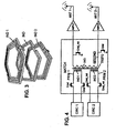
- the three inductors IND1, IND2, IND are represented in this Figure. These inductors are substantially flat inductors (in the sense indicated above), each comprising a given number of octagonal turns.
- inductors are created using integrated circuit etching processes known to a person skilled in the art, for example by photolithography.
- the inductor IND comprised in the secondary circuit of the transformer is located between the coils IND1 and IND2 of the primary circuits PRIM1 and PRIM2.
- the inductors are concentrically arranged to ensure satisfactory magnetic coupling.
- the inductor IND1 comprises four turns while the inductor IND2 comprises three.
- the circuits PRIM1 and PRIM2 therefore have different transformation ratios.
- the transformation ratio is the ratio of the number of turns in the secondary to the number of turns in the primary.
- each of the inductors are mostly coplanar. These coplanar parts can therefore be in the same circuit layer.
- the inductors also comprise certain parts which form bridges between different turns. These bridge-forming parts may be comprised in layers adjacent to those which comprise the substantially coplanar turns.
- the circuit MATCH is controlled by means of a set of transistors.
- transistors are arranged so that they operate as switches on the branches of the circuits PRIM1, PRIM2 and SECOND.
- the transistors on the circuit PRIM1 and the transistor on the branch of the circuit SECOND coupled to the amplifier AMPLI2 are controlled by a signal Cmd.
- the other transistors are controlled by a signal Cmd_not which is the complement of the signal Cmd.
- the transistors coupled to the secondary circuit have their drain connected to the secondary and their source to the ground.
- the signal Cmd is activated which enables the transistors controlled by this signal to pass current.
- the circuit PRIM1 closes, the secondary branch connected to AMPLI2 goes to the ground, and the transistor on the secondary branch connected to AMPLI1 does not pass current.
- the signal Cmd is deactivated which enables the transistors controlled by the signal Cmd_not to pass current.
- the circuit PRIM1 opens and the circuit CIRC2 closes, the secondary branch connected to AMPLI1 goes to the ground, and the transistor on the secondary branch connected to AMPLI2 does not pass current.
- the transistors on the circuits PRIM1 and PRIM2 have been replaced by two variable impedance circuits IMPED1 and IMPED2.
- Each of these circuits is controlled by a current source, which itself is controlled by the signal Cmd for the current source controlling the circuit IMPED1, and the signal Cmd_not for the current source controlling the circuit IMPED2.
- the circuits IMPED1 and IMPED2 are operational amplifiers.
- the current sources are coupled to the amplifiers to obtain an output impendence of the operational amplifiers which is zero or infinite (theoretically).
- a communication terminal according to an embodiment of the invention is now described with reference to Figure 6 .
- the terminal TERM comprises a processing unit PROC for controlling the terminal.
- the terminal additionally comprises a communication unit COM and an antenna ANT for communication purposes.
- the terminal additionally comprises a matching circuit MATCH comprising a circuit of the invention.
Landscapes
- Engineering & Computer Science (AREA)
- Power Engineering (AREA)
- Multimedia (AREA)
- Semiconductor Integrated Circuits (AREA)
- Input Circuits Of Receivers And Coupling Of Receivers And Audio Equipment (AREA)
- Amplifiers (AREA)
- Transmitters (AREA)
Claims (8)
- Integrierte Funkfrequenzschaltung aufweisend einen Transformator (TRSFO) mit einer ersten primären Schaltung (PRIM1), einer zweiten primären Schaltung (PRIM2) und einer sekundären Schaltung, wobei die sekundäre Schaltung (SECOND) einen ersten integrierten Induktor (IND) aufweist, wobei der erste Induktor auf einer Achse, welche orthogonal zu einer Oberfläche der Schaltung ist, zwischen jeweils einem zweiten (IND1) und einem dritten (IND3) integrierten Induktor positioniert ist, welche in der ersten primären Schaltung und der zweiten primären Schaltung vorgesehen sind, und wobei die Schaltung mehrlagig ist und der erste, der zweite und der dritte Induktor im Wesentlichen flach sind und wobei jeder dieser Induktoren jeweils nur in einer entsprechende Lage der Funkfrequenzschaltung vorgesehen ist.
- Schaltung nach Anspruch 1, wobei die Induktoren eine vorgegebenen Anzahl N von konzentrischen Windungen aufweisen, wobei N eine ganze Zahl größer als 1 ist.
- Schaltung nach einem der obigen Ansprüche, wobei der Transformator in einer Anpassstufe (MATCH) der Funkfrequenzschaltung positioniert ist, so dass er eine Anpassung zwischen der Funkfrequenzschaltung und zumindest einer Antenne (ANT1, ANT2) durchführt.
- Schaltung nach einem der obigen Ansprüche, wobei die erste und die zweite primäre Schaltung unterschiedliche Transformationsverhältnisse haben.
- Schaltung nach einem der obigen Ansprüche, des Weiteren aufweisend eine Steuereinheit für die erste und zweite primäre Schaltung, wobei die Steuereinheit so ausgestaltet ist, dass nur eine primäre Schaltung aus der ersten und der zweiten primären Schaltung gleichzeitig betrieben wird.
- Schaltung nach Anspruch 5, wobei die Steuereinheit Schalter zum elektrischen und ausgewählten Isolieren einer der ersten und zweiten primären Schaltung aufweist.
- Schaltung nach Anspruch 5, wobei die Steuereinheit stromstärkensteuerungsvariable Impedanzschaltungen zum elektrischen und selektiven Isolieren einer der ersten und zweiten primären Schaltungen aufweist.
- Kommunikationsendgerät (TERM) aufweisend:- eine Kommunikationseinheit (COM);- mindestens eine Antenne (ANT);wobei das Endgerät zusätzlich aufweist:eine Anpassungsschaltung (MATCH) nach einem der Ansprüche 1 bis 7 zwischen der Kommunikationseinheit und der mindestens einen Antenne.
Applications Claiming Priority (2)
| Application Number | Priority Date | Filing Date | Title |
|---|---|---|---|
| FR0957129 | 2009-10-12 | ||
| PCT/EP2010/065274 WO2011045312A1 (en) | 2009-10-12 | 2010-10-12 | Integrated transformer with multiple transformation ratios |
Publications (2)
| Publication Number | Publication Date |
|---|---|
| EP2489048A1 EP2489048A1 (de) | 2012-08-22 |
| EP2489048B1 true EP2489048B1 (de) | 2014-12-31 |
Family
ID=42153681
Family Applications (1)
| Application Number | Title | Priority Date | Filing Date |
|---|---|---|---|
| EP10768722.0A Not-in-force EP2489048B1 (de) | 2009-10-12 | 2010-10-12 | Integrierter transformator mit mehreren transformationsverhältnissen |
Country Status (4)
| Country | Link |
|---|---|
| US (1) | US9064627B2 (de) |
| EP (1) | EP2489048B1 (de) |
| CN (1) | CN102714084B (de) |
| WO (1) | WO2011045312A1 (de) |
Families Citing this family (18)
| Publication number | Priority date | Publication date | Assignee | Title |
|---|---|---|---|---|
| EP2329581A4 (de) | 2008-09-03 | 2013-12-04 | Exro Technologies Inc | Leistungsumwandlungssystem für einen mehrstufigen generator |
| EP2474092B1 (de) * | 2009-09-03 | 2020-04-29 | DPM Technologies Inc. | System, vorrichtung und verfahren für variable spulenkonfigurationen |
| WO2012114983A1 (ja) * | 2011-02-23 | 2012-08-30 | 株式会社村田製作所 | インピーダンス変換回路および通信端末装置 |
| US9306502B2 (en) | 2011-05-09 | 2016-04-05 | Qualcomm Incorporated | System providing switchable impedance transformer matching for power amplifiers |
| US8970297B2 (en) | 2012-03-19 | 2015-03-03 | Qualcomm Incorporated | Reconfigurable input power distribution doherty amplifier with improved efficiency |
| US9431473B2 (en) * | 2012-11-21 | 2016-08-30 | Qualcomm Incorporated | Hybrid transformer structure on semiconductor devices |
| US9031518B2 (en) | 2012-12-17 | 2015-05-12 | Qualcomm Incorporated | Concurrent hybrid matching network |
| US10002700B2 (en) | 2013-02-27 | 2018-06-19 | Qualcomm Incorporated | Vertical-coupling transformer with an air-gap structure |
| US9634645B2 (en) | 2013-03-14 | 2017-04-25 | Qualcomm Incorporated | Integration of a replica circuit and a transformer above a dielectric substrate |
| US9449753B2 (en) | 2013-08-30 | 2016-09-20 | Qualcomm Incorporated | Varying thickness inductor |
| US9906318B2 (en) | 2014-04-18 | 2018-02-27 | Qualcomm Incorporated | Frequency multiplexer |
| US9871488B2 (en) * | 2015-01-28 | 2018-01-16 | Qualcomm Incorporated | Dual-mode power amplifier |
| EP3586431A4 (de) | 2017-05-23 | 2020-11-11 | DPM Technologies Inc. | Steuerung, vorrichtung und verfahren für ein variables spulenkonfigurationssystem |
| CA3111823A1 (en) | 2018-09-05 | 2020-03-12 | Dpm Technologies Inc. | Systems and methods for intelligent energy storage and provisioning using an energy storage control system |
| WO2020215154A1 (en) | 2019-04-23 | 2020-10-29 | Dpm Technologies Inc. | Fault tolerant rotating electric machine |
| KR102815800B1 (ko) * | 2020-12-15 | 2025-06-02 | 삼성전자주식회사 | 저손실을 위한 트랜스포머 및 이를 포함하는 장치 |
| US11897362B2 (en) | 2021-05-04 | 2024-02-13 | Exro Technologies Inc. | Systems and methods for individual control of a plurality of controllable units of battery cells |
| EP4324089A4 (de) | 2021-05-13 | 2024-10-23 | Exro Technologies Inc. | Verfahren und vorrichtung zum antreiben von spulen einer mehrphasigen elektrischen maschine |
Family Cites Families (5)
| Publication number | Priority date | Publication date | Assignee | Title |
|---|---|---|---|---|
| US6731166B1 (en) * | 2001-11-26 | 2004-05-04 | Analog Devices, Inc. | Power amplifier system with multiple primary windings |
| US7292126B2 (en) * | 2004-04-30 | 2007-11-06 | Astec International Limited | Low noise planar transformer |
| US7675365B2 (en) | 2007-01-10 | 2010-03-09 | Samsung Electro-Mechanics | Systems and methods for power amplifiers with voltage boosting multi-primary transformers |
| US7576607B2 (en) * | 2008-01-03 | 2009-08-18 | Samsung Electro-Mechanics | Multi-segment primary and multi-turn secondary transformer for power amplifier systems |
| US7489226B1 (en) * | 2008-05-09 | 2009-02-10 | Raytheon Company | Fabrication method and structure for embedded core transformers |
-
2010
- 2010-10-12 EP EP10768722.0A patent/EP2489048B1/de not_active Not-in-force
- 2010-10-12 US US13/500,679 patent/US9064627B2/en not_active Expired - Fee Related
- 2010-10-12 CN CN201080053684.1A patent/CN102714084B/zh not_active Expired - Fee Related
- 2010-10-12 WO PCT/EP2010/065274 patent/WO2011045312A1/en not_active Ceased
Also Published As
| Publication number | Publication date |
|---|---|
| EP2489048A1 (de) | 2012-08-22 |
| US9064627B2 (en) | 2015-06-23 |
| CN102714084B (zh) | 2015-12-02 |
| WO2011045312A1 (en) | 2011-04-21 |
| CN102714084A (zh) | 2012-10-03 |
| US20120194403A1 (en) | 2012-08-02 |
Similar Documents
| Publication | Publication Date | Title |
|---|---|---|
| EP2489048B1 (de) | Integrierter transformator mit mehreren transformationsverhältnissen | |
| EP2761633B1 (de) | Schaltbarer transformator mit eingebetteten schaltern in den wicklungen | |
| US7576607B2 (en) | Multi-segment primary and multi-turn secondary transformer for power amplifier systems | |
| US7526256B2 (en) | Transformer-based multi-band RF front-end architecture | |
| US8072287B2 (en) | Method and system for configurable differential or single-ended signaling in an integrated circuit | |
| US11349506B2 (en) | Radio frequency module and communication device | |
| US11757478B2 (en) | Radio frequency module and communication device | |
| US7812701B2 (en) | Compact multiple transformers | |
| US9755610B2 (en) | Transformer of the balanced-unbalanced type | |
| JP2005117467A (ja) | 高周波スイッチ装置 | |
| GB2445677A (en) | An integrated impedance-matching power combiner using a transformer with multiple primary windings | |
| US11394421B2 (en) | Radio frequency module and communication device | |
| JP6597461B2 (ja) | 増幅回路 | |
| US11476810B2 (en) | Radio-frequency circuit | |
| US10411657B2 (en) | Two-stage electromagnetic induction transformer | |
| US8145160B2 (en) | Tx module for wireless communication | |
| WO2018123914A1 (ja) | 高周波モジュール及び通信装置 | |
| KR101721866B1 (ko) | 위상 천이기 및 그 제어방법 | |
| KR102442302B1 (ko) | 고주파 모듈 및 통신 장치 | |
| CN107040219B (zh) | 完全集成低噪声放大器 | |
| CN112702071B (zh) | 双频带混频器 | |
| US20160191106A1 (en) | Front end circuit | |
| JP6466872B2 (ja) | 通信回路 | |
| US20250080067A1 (en) | Bandwidth tuning using single-input multiple-output low-noise amplifier | |
| Ngo et al. | A compact 6-bit phase shifter in 65 nm RF CMOS technology for ISM band |
Legal Events
| Date | Code | Title | Description |
|---|---|---|---|
| PUAI | Public reference made under article 153(3) epc to a published international application that has entered the european phase |
Free format text: ORIGINAL CODE: 0009012 |
|
| 17P | Request for examination filed |
Effective date: 20120405 |
|
| AK | Designated contracting states |
Kind code of ref document: A1 Designated state(s): AL AT BE BG CH CY CZ DE DK EE ES FI FR GB GR HR HU IE IS IT LI LT LU LV MC MK MT NL NO PL PT RO RS SE SI SK SM TR |
|
| DAX | Request for extension of the european patent (deleted) | ||
| GRAP | Despatch of communication of intention to grant a patent |
Free format text: ORIGINAL CODE: EPIDOSNIGR1 |
|
| INTG | Intention to grant announced |
Effective date: 20140826 |
|
| INTG | Intention to grant announced |
Effective date: 20140902 |
|
| GRAS | Grant fee paid |
Free format text: ORIGINAL CODE: EPIDOSNIGR3 |
|
| GRAA | (expected) grant |
Free format text: ORIGINAL CODE: 0009210 |
|
| AK | Designated contracting states |
Kind code of ref document: B1 Designated state(s): AL AT BE BG CH CY CZ DE DK EE ES FI FR GB GR HR HU IE IS IT LI LT LU LV MC MK MT NL NO PL PT RO RS SE SI SK SM TR |
|
| REG | Reference to a national code |
Ref country code: CH Ref legal event code: EP Ref country code: GB Ref legal event code: FG4D |
|
| REG | Reference to a national code |
Ref country code: IE Ref legal event code: FG4D |
|
| REG | Reference to a national code |
Ref country code: AT Ref legal event code: REF Ref document number: 704823 Country of ref document: AT Kind code of ref document: T Effective date: 20150215 |
|
| REG | Reference to a national code |
Ref country code: DE Ref legal event code: R096 Ref document number: 602010021467 Country of ref document: DE Effective date: 20150226 |
|
| PG25 | Lapsed in a contracting state [announced via postgrant information from national office to epo] |
Ref country code: FI Free format text: LAPSE BECAUSE OF FAILURE TO SUBMIT A TRANSLATION OF THE DESCRIPTION OR TO PAY THE FEE WITHIN THE PRESCRIBED TIME-LIMIT Effective date: 20141231 Ref country code: NO Free format text: LAPSE BECAUSE OF FAILURE TO SUBMIT A TRANSLATION OF THE DESCRIPTION OR TO PAY THE FEE WITHIN THE PRESCRIBED TIME-LIMIT Effective date: 20150331 Ref country code: LT Free format text: LAPSE BECAUSE OF FAILURE TO SUBMIT A TRANSLATION OF THE DESCRIPTION OR TO PAY THE FEE WITHIN THE PRESCRIBED TIME-LIMIT Effective date: 20141231 |
|
| REG | Reference to a national code |
Ref country code: NL Ref legal event code: VDEP Effective date: 20141231 |
|
| REG | Reference to a national code |
Ref country code: LT Ref legal event code: MG4D |
|
| PG25 | Lapsed in a contracting state [announced via postgrant information from national office to epo] |
Ref country code: HR Free format text: LAPSE BECAUSE OF FAILURE TO SUBMIT A TRANSLATION OF THE DESCRIPTION OR TO PAY THE FEE WITHIN THE PRESCRIBED TIME-LIMIT Effective date: 20141231 Ref country code: SE Free format text: LAPSE BECAUSE OF FAILURE TO SUBMIT A TRANSLATION OF THE DESCRIPTION OR TO PAY THE FEE WITHIN THE PRESCRIBED TIME-LIMIT Effective date: 20141231 Ref country code: GR Free format text: LAPSE BECAUSE OF FAILURE TO SUBMIT A TRANSLATION OF THE DESCRIPTION OR TO PAY THE FEE WITHIN THE PRESCRIBED TIME-LIMIT Effective date: 20150401 Ref country code: RS Free format text: LAPSE BECAUSE OF FAILURE TO SUBMIT A TRANSLATION OF THE DESCRIPTION OR TO PAY THE FEE WITHIN THE PRESCRIBED TIME-LIMIT Effective date: 20141231 Ref country code: LV Free format text: LAPSE BECAUSE OF FAILURE TO SUBMIT A TRANSLATION OF THE DESCRIPTION OR TO PAY THE FEE WITHIN THE PRESCRIBED TIME-LIMIT Effective date: 20141231 |
|
| REG | Reference to a national code |
Ref country code: AT Ref legal event code: MK05 Ref document number: 704823 Country of ref document: AT Kind code of ref document: T Effective date: 20141231 |
|
| PG25 | Lapsed in a contracting state [announced via postgrant information from national office to epo] |
Ref country code: NL Free format text: LAPSE BECAUSE OF FAILURE TO SUBMIT A TRANSLATION OF THE DESCRIPTION OR TO PAY THE FEE WITHIN THE PRESCRIBED TIME-LIMIT Effective date: 20141231 |
|
| PG25 | Lapsed in a contracting state [announced via postgrant information from national office to epo] |
Ref country code: SK Free format text: LAPSE BECAUSE OF FAILURE TO SUBMIT A TRANSLATION OF THE DESCRIPTION OR TO PAY THE FEE WITHIN THE PRESCRIBED TIME-LIMIT Effective date: 20141231 Ref country code: RO Free format text: LAPSE BECAUSE OF FAILURE TO SUBMIT A TRANSLATION OF THE DESCRIPTION OR TO PAY THE FEE WITHIN THE PRESCRIBED TIME-LIMIT Effective date: 20141231 Ref country code: ES Free format text: LAPSE BECAUSE OF FAILURE TO SUBMIT A TRANSLATION OF THE DESCRIPTION OR TO PAY THE FEE WITHIN THE PRESCRIBED TIME-LIMIT Effective date: 20141231 Ref country code: CZ Free format text: LAPSE BECAUSE OF FAILURE TO SUBMIT A TRANSLATION OF THE DESCRIPTION OR TO PAY THE FEE WITHIN THE PRESCRIBED TIME-LIMIT Effective date: 20141231 |
|
| PG25 | Lapsed in a contracting state [announced via postgrant information from national office to epo] |
Ref country code: AT Free format text: LAPSE BECAUSE OF FAILURE TO SUBMIT A TRANSLATION OF THE DESCRIPTION OR TO PAY THE FEE WITHIN THE PRESCRIBED TIME-LIMIT Effective date: 20141231 Ref country code: IS Free format text: LAPSE BECAUSE OF FAILURE TO SUBMIT A TRANSLATION OF THE DESCRIPTION OR TO PAY THE FEE WITHIN THE PRESCRIBED TIME-LIMIT Effective date: 20150430 Ref country code: PL Free format text: LAPSE BECAUSE OF FAILURE TO SUBMIT A TRANSLATION OF THE DESCRIPTION OR TO PAY THE FEE WITHIN THE PRESCRIBED TIME-LIMIT Effective date: 20141231 |
|
| REG | Reference to a national code |
Ref country code: FR Ref legal event code: PLFP Year of fee payment: 6 |
|
| REG | Reference to a national code |
Ref country code: DE Ref legal event code: R097 Ref document number: 602010021467 Country of ref document: DE |
|
| PG25 | Lapsed in a contracting state [announced via postgrant information from national office to epo] |
Ref country code: DK Free format text: LAPSE BECAUSE OF FAILURE TO SUBMIT A TRANSLATION OF THE DESCRIPTION OR TO PAY THE FEE WITHIN THE PRESCRIBED TIME-LIMIT Effective date: 20141231 Ref country code: EE Free format text: LAPSE BECAUSE OF FAILURE TO SUBMIT A TRANSLATION OF THE DESCRIPTION OR TO PAY THE FEE WITHIN THE PRESCRIBED TIME-LIMIT Effective date: 20141231 |
|
| PLBE | No opposition filed within time limit |
Free format text: ORIGINAL CODE: 0009261 |
|
| STAA | Information on the status of an ep patent application or granted ep patent |
Free format text: STATUS: NO OPPOSITION FILED WITHIN TIME LIMIT |
|
| 26N | No opposition filed |
Effective date: 20151001 |
|
| PG25 | Lapsed in a contracting state [announced via postgrant information from national office to epo] |
Ref country code: IT Free format text: LAPSE BECAUSE OF FAILURE TO SUBMIT A TRANSLATION OF THE DESCRIPTION OR TO PAY THE FEE WITHIN THE PRESCRIBED TIME-LIMIT Effective date: 20141231 |
|
| PG25 | Lapsed in a contracting state [announced via postgrant information from national office to epo] |
Ref country code: SI Free format text: LAPSE BECAUSE OF FAILURE TO SUBMIT A TRANSLATION OF THE DESCRIPTION OR TO PAY THE FEE WITHIN THE PRESCRIBED TIME-LIMIT Effective date: 20141231 |
|
| PG25 | Lapsed in a contracting state [announced via postgrant information from national office to epo] |
Ref country code: LU Free format text: LAPSE BECAUSE OF FAILURE TO SUBMIT A TRANSLATION OF THE DESCRIPTION OR TO PAY THE FEE WITHIN THE PRESCRIBED TIME-LIMIT Effective date: 20151012 Ref country code: BE Free format text: LAPSE BECAUSE OF FAILURE TO SUBMIT A TRANSLATION OF THE DESCRIPTION OR TO PAY THE FEE WITHIN THE PRESCRIBED TIME-LIMIT Effective date: 20141231 |
|
| REG | Reference to a national code |
Ref country code: CH Ref legal event code: PL |
|
| PG25 | Lapsed in a contracting state [announced via postgrant information from national office to epo] |
Ref country code: MC Free format text: LAPSE BECAUSE OF FAILURE TO SUBMIT A TRANSLATION OF THE DESCRIPTION OR TO PAY THE FEE WITHIN THE PRESCRIBED TIME-LIMIT Effective date: 20141231 |
|
| REG | Reference to a national code |
Ref country code: IE Ref legal event code: MM4A |
|
| PG25 | Lapsed in a contracting state [announced via postgrant information from national office to epo] |
Ref country code: LI Free format text: LAPSE BECAUSE OF NON-PAYMENT OF DUE FEES Effective date: 20151031 Ref country code: CH Free format text: LAPSE BECAUSE OF NON-PAYMENT OF DUE FEES Effective date: 20151031 |
|
| REG | Reference to a national code |
Ref country code: FR Ref legal event code: PLFP Year of fee payment: 7 |
|
| PG25 | Lapsed in a contracting state [announced via postgrant information from national office to epo] |
Ref country code: IE Free format text: LAPSE BECAUSE OF NON-PAYMENT OF DUE FEES Effective date: 20151012 |
|
| REG | Reference to a national code |
Ref country code: FR Ref legal event code: TP Owner name: ST-ERICSSON SA, CH Effective date: 20161003 |
|
| PG25 | Lapsed in a contracting state [announced via postgrant information from national office to epo] |
Ref country code: SM Free format text: LAPSE BECAUSE OF FAILURE TO SUBMIT A TRANSLATION OF THE DESCRIPTION OR TO PAY THE FEE WITHIN THE PRESCRIBED TIME-LIMIT Effective date: 20141231 Ref country code: BG Free format text: LAPSE BECAUSE OF FAILURE TO SUBMIT A TRANSLATION OF THE DESCRIPTION OR TO PAY THE FEE WITHIN THE PRESCRIBED TIME-LIMIT Effective date: 20141231 Ref country code: HU Free format text: LAPSE BECAUSE OF FAILURE TO SUBMIT A TRANSLATION OF THE DESCRIPTION OR TO PAY THE FEE WITHIN THE PRESCRIBED TIME-LIMIT; INVALID AB INITIO Effective date: 20101012 |
|
| PG25 | Lapsed in a contracting state [announced via postgrant information from national office to epo] |
Ref country code: CY Free format text: LAPSE BECAUSE OF FAILURE TO SUBMIT A TRANSLATION OF THE DESCRIPTION OR TO PAY THE FEE WITHIN THE PRESCRIBED TIME-LIMIT Effective date: 20141231 |
|
| PG25 | Lapsed in a contracting state [announced via postgrant information from national office to epo] |
Ref country code: MT Free format text: LAPSE BECAUSE OF FAILURE TO SUBMIT A TRANSLATION OF THE DESCRIPTION OR TO PAY THE FEE WITHIN THE PRESCRIBED TIME-LIMIT Effective date: 20141231 Ref country code: TR Free format text: LAPSE BECAUSE OF FAILURE TO SUBMIT A TRANSLATION OF THE DESCRIPTION OR TO PAY THE FEE WITHIN THE PRESCRIBED TIME-LIMIT Effective date: 20141231 |
|
| REG | Reference to a national code |
Ref country code: DE Ref legal event code: R082 Ref document number: 602010021467 Country of ref document: DE Representative=s name: GRUENECKER PATENT- UND RECHTSANWAELTE PARTG MB, DE |
|
| REG | Reference to a national code |
Ref country code: FR Ref legal event code: PLFP Year of fee payment: 8 |
|
| PGFP | Annual fee paid to national office [announced via postgrant information from national office to epo] |
Ref country code: FR Payment date: 20170921 Year of fee payment: 8 Ref country code: GB Payment date: 20170925 Year of fee payment: 8 |
|
| PGFP | Annual fee paid to national office [announced via postgrant information from national office to epo] |
Ref country code: DE Payment date: 20170920 Year of fee payment: 8 |
|
| REG | Reference to a national code |
Ref country code: FR Ref legal event code: TP Owner name: OCT CIRCUIT TECHNOLOGIES INTERNATIONAL LIMITED, IE Effective date: 20180116 |
|
| PG25 | Lapsed in a contracting state [announced via postgrant information from national office to epo] |
Ref country code: MK Free format text: LAPSE BECAUSE OF FAILURE TO SUBMIT A TRANSLATION OF THE DESCRIPTION OR TO PAY THE FEE WITHIN THE PRESCRIBED TIME-LIMIT Effective date: 20141231 |
|
| PG25 | Lapsed in a contracting state [announced via postgrant information from national office to epo] |
Ref country code: PT Free format text: LAPSE BECAUSE OF FAILURE TO SUBMIT A TRANSLATION OF THE DESCRIPTION OR TO PAY THE FEE WITHIN THE PRESCRIBED TIME-LIMIT Effective date: 20141231 |
|
| PG25 | Lapsed in a contracting state [announced via postgrant information from national office to epo] |
Ref country code: AL Free format text: LAPSE BECAUSE OF FAILURE TO SUBMIT A TRANSLATION OF THE DESCRIPTION OR TO PAY THE FEE WITHIN THE PRESCRIBED TIME-LIMIT Effective date: 20141231 |
|
| REG | Reference to a national code |
Ref country code: DE Ref legal event code: R119 Ref document number: 602010021467 Country of ref document: DE |
|
| GBPC | Gb: european patent ceased through non-payment of renewal fee |
Effective date: 20181012 |
|
| PG25 | Lapsed in a contracting state [announced via postgrant information from national office to epo] |
Ref country code: DE Free format text: LAPSE BECAUSE OF NON-PAYMENT OF DUE FEES Effective date: 20190501 |
|
| PG25 | Lapsed in a contracting state [announced via postgrant information from national office to epo] |
Ref country code: FR Free format text: LAPSE BECAUSE OF NON-PAYMENT OF DUE FEES Effective date: 20181031 |
|
| PG25 | Lapsed in a contracting state [announced via postgrant information from national office to epo] |
Ref country code: GB Free format text: LAPSE BECAUSE OF NON-PAYMENT OF DUE FEES Effective date: 20181012 |