EP2490273A1 - Method for manufacturing a HTS coated tape with laser beam cutting - Google Patents
Method for manufacturing a HTS coated tape with laser beam cutting Download PDFInfo
- Publication number
- EP2490273A1 EP2490273A1 EP11154950A EP11154950A EP2490273A1 EP 2490273 A1 EP2490273 A1 EP 2490273A1 EP 11154950 A EP11154950 A EP 11154950A EP 11154950 A EP11154950 A EP 11154950A EP 2490273 A1 EP2490273 A1 EP 2490273A1
- Authority
- EP
- European Patent Office
- Prior art keywords
- laser beam
- deposition
- tape
- hts
- layer
- Prior art date
- Legal status (The legal status is an assumption and is not a legal conclusion. Google has not performed a legal analysis and makes no representation as to the accuracy of the status listed.)
- Granted
Links
- 238000005520 cutting process Methods 0.000 title claims abstract description 81
- 238000000034 method Methods 0.000 title claims abstract description 37
- 238000004519 manufacturing process Methods 0.000 title claims abstract description 12
- 238000000151 deposition Methods 0.000 claims abstract description 56
- 230000008021 deposition Effects 0.000 claims abstract description 55
- 239000000758 substrate Substances 0.000 claims abstract description 25
- 239000007788 liquid Substances 0.000 claims abstract description 24
- 239000002887 superconductor Substances 0.000 claims abstract description 5
- 238000002360 preparation method Methods 0.000 claims abstract description 3
- 239000007789 gas Substances 0.000 claims description 13
- 238000000137 annealing Methods 0.000 claims description 5
- 239000010970 precious metal Substances 0.000 claims description 5
- QVGXLLKOCUKJST-UHFFFAOYSA-N atomic oxygen Chemical compound [O] QVGXLLKOCUKJST-UHFFFAOYSA-N 0.000 claims description 3
- 239000001301 oxygen Substances 0.000 claims description 3
- 229910052760 oxygen Inorganic materials 0.000 claims description 3
- 229910000923 precious metal alloy Inorganic materials 0.000 claims description 3
- 238000007747 plating Methods 0.000 claims description 2
- 238000001771 vacuum deposition Methods 0.000 claims description 2
- 230000006866 deterioration Effects 0.000 abstract description 6
- 239000000463 material Substances 0.000 description 11
- 239000004020 conductor Substances 0.000 description 8
- LYCAIKOWRPUZTN-UHFFFAOYSA-N Ethylene glycol Chemical compound OCCO LYCAIKOWRPUZTN-UHFFFAOYSA-N 0.000 description 3
- 238000005530 etching Methods 0.000 description 3
- 239000002184 metal Substances 0.000 description 3
- 229910052751 metal Inorganic materials 0.000 description 3
- 229910052709 silver Inorganic materials 0.000 description 3
- 238000003892 spreading Methods 0.000 description 3
- XLYOFNOQVPJJNP-UHFFFAOYSA-N water Substances O XLYOFNOQVPJJNP-UHFFFAOYSA-N 0.000 description 3
- IJGRMHOSHXDMSA-UHFFFAOYSA-N Atomic nitrogen Chemical compound N#N IJGRMHOSHXDMSA-UHFFFAOYSA-N 0.000 description 2
- RYGMFSIKBFXOCR-UHFFFAOYSA-N Copper Chemical compound [Cu] RYGMFSIKBFXOCR-UHFFFAOYSA-N 0.000 description 2
- 238000010521 absorption reaction Methods 0.000 description 2
- CETPSERCERDGAM-UHFFFAOYSA-N ceric oxide Chemical compound O=[Ce]=O CETPSERCERDGAM-UHFFFAOYSA-N 0.000 description 2
- 229910000422 cerium(IV) oxide Inorganic materials 0.000 description 2
- 238000001816 cooling Methods 0.000 description 2
- 229910052802 copper Inorganic materials 0.000 description 2
- 239000010949 copper Substances 0.000 description 2
- 229910052737 gold Inorganic materials 0.000 description 2
- 239000010931 gold Substances 0.000 description 2
- 239000012535 impurity Substances 0.000 description 2
- 238000003698 laser cutting Methods 0.000 description 2
- 229910000510 noble metal Inorganic materials 0.000 description 2
- 230000003287 optical effect Effects 0.000 description 2
- 239000004332 silver Substances 0.000 description 2
- 230000006641 stabilisation Effects 0.000 description 2
- 238000011105 stabilization Methods 0.000 description 2
- 239000010935 stainless steel Substances 0.000 description 2
- 229910001220 stainless steel Inorganic materials 0.000 description 2
- LFQSCWFLJHTTHZ-UHFFFAOYSA-N Ethanol Chemical compound CCO LFQSCWFLJHTTHZ-UHFFFAOYSA-N 0.000 description 1
- XUIMIQQOPSSXEZ-UHFFFAOYSA-N Silicon Chemical compound [Si] XUIMIQQOPSSXEZ-UHFFFAOYSA-N 0.000 description 1
- 229910003098 YBa2Cu3O7−x Inorganic materials 0.000 description 1
- 230000002411 adverse Effects 0.000 description 1
- 238000010420 art technique Methods 0.000 description 1
- 230000009286 beneficial effect Effects 0.000 description 1
- 230000005540 biological transmission Effects 0.000 description 1
- 238000009835 boiling Methods 0.000 description 1
- 239000000919 ceramic Substances 0.000 description 1
- 238000006243 chemical reaction Methods 0.000 description 1
- 230000007797 corrosion Effects 0.000 description 1
- 238000005260 corrosion Methods 0.000 description 1
- 230000032798 delamination Effects 0.000 description 1
- 238000009826 distribution Methods 0.000 description 1
- 230000000694 effects Effects 0.000 description 1
- 238000009713 electroplating Methods 0.000 description 1
- 238000005516 engineering process Methods 0.000 description 1
- 229940093476 ethylene glycol Drugs 0.000 description 1
- 239000000835 fiber Substances 0.000 description 1
- PCHJSUWPFVWCPO-UHFFFAOYSA-N gold Chemical compound [Au] PCHJSUWPFVWCPO-UHFFFAOYSA-N 0.000 description 1
- 239000011344 liquid material Substances 0.000 description 1
- 239000012263 liquid product Substances 0.000 description 1
- 229910052757 nitrogen Inorganic materials 0.000 description 1
- 230000035515 penetration Effects 0.000 description 1
- 238000004549 pulsed laser deposition Methods 0.000 description 1
- 239000004065 semiconductor Substances 0.000 description 1
- 229910052710 silicon Inorganic materials 0.000 description 1
- 239000010703 silicon Substances 0.000 description 1
- 239000003381 stabilizer Substances 0.000 description 1
- 239000000126 substance Substances 0.000 description 1
- 235000012431 wafers Nutrition 0.000 description 1
- 229910001233 yttria-stabilized zirconia Inorganic materials 0.000 description 1
Images

Classifications
-
- H—ELECTRICITY
- H10—SEMICONDUCTOR DEVICES; ELECTRIC SOLID-STATE DEVICES NOT OTHERWISE PROVIDED FOR
- H10N—ELECTRIC SOLID-STATE DEVICES NOT OTHERWISE PROVIDED FOR
- H10N60/00—Superconducting devices
- H10N60/01—Manufacture or treatment
-
- H—ELECTRICITY
- H10—SEMICONDUCTOR DEVICES; ELECTRIC SOLID-STATE DEVICES NOT OTHERWISE PROVIDED FOR
- H10N—ELECTRIC SOLID-STATE DEVICES NOT OTHERWISE PROVIDED FOR
- H10N60/00—Superconducting devices
- H10N60/01—Manufacture or treatment
- H10N60/0268—Manufacture or treatment of devices comprising copper oxide
- H10N60/0661—Processes performed after copper oxide formation, e.g. patterning
-
- H—ELECTRICITY
- H10—SEMICONDUCTOR DEVICES; ELECTRIC SOLID-STATE DEVICES NOT OTHERWISE PROVIDED FOR
- H10N—ELECTRIC SOLID-STATE DEVICES NOT OTHERWISE PROVIDED FOR
- H10N60/00—Superconducting devices
- H10N60/01—Manufacture or treatment
- H10N60/0268—Manufacture or treatment of devices comprising copper oxide
- H10N60/0801—Manufacture or treatment of filaments or composite wires
-
- Y—GENERAL TAGGING OF NEW TECHNOLOGICAL DEVELOPMENTS; GENERAL TAGGING OF CROSS-SECTIONAL TECHNOLOGIES SPANNING OVER SEVERAL SECTIONS OF THE IPC; TECHNICAL SUBJECTS COVERED BY FORMER USPC CROSS-REFERENCE ART COLLECTIONS [XRACs] AND DIGESTS
- Y10—TECHNICAL SUBJECTS COVERED BY FORMER USPC
- Y10T—TECHNICAL SUBJECTS COVERED BY FORMER US CLASSIFICATION
- Y10T29/00—Metal working
- Y10T29/49—Method of mechanical manufacture
- Y10T29/49002—Electrical device making
- Y10T29/49014—Superconductor
Definitions
- the gas flow and/or liquid flow is chemically active with respect to the substrate tape.
- the gas flow and/or liquid flow is inert with respect to all other components of the partially prepared HTS coated tape.
- the invention presents a novel method for manufacturing of a HTS coated tape. It comprises a processing of a substrate tape, a deposition of at least one buffer layer, a deposition of a HTS film, a deposition of a metallic protection layer, a deposition of a metallic shunt layer, and a cutting of the tape in order to provide a desired tape form.
- the cutting of the tape is performed via a laser beam cutting. Later technique is typically applied together with a liquid flow directed along the laser beam and guiding this beam towards the tape. In accordance with the invention, the laser beam cutting is applied in between processing steps prior to the deposition of the metallic shunt layer.
- a buffer layer 2 (or alternatively several buffer layers) is deposited.
- a HTS film 3 is deposited.
- a first part 5 of a metallic protection layer is deposited on top of the HTS film 3.
- a partly prepared HTS coated tape 10 prepared in this way is illustrated in Fig. 1a .
- the relative transporting may be smooth, and typically with constant speed; transport is preferably an "in-plane" transport with respect to the tape (i.e. from left to right and up and down in the drawing plane of Fig. 2a , see below); 1 D (linear) or 2D transport are possible.
- the transport and the laser cutting may be alternatively provided with at least one interruption; there may be a multitude of cutting interruptions during the processing if desired.
Landscapes
- Engineering & Computer Science (AREA)
- Manufacturing & Machinery (AREA)
- Superconductors And Manufacturing Methods Therefor (AREA)
- Laser Beam Processing (AREA)
Abstract
a) preparation of a substrate tape (1),
b) deposition of at least one buffer layer (2),
c) deposition of an HTS film (3),
d) deposition of a metallic protection layer (35) on the HTS film (3),
e) deposition of a metallic shunt layer (36),
is characterized in that earlier than the deposition of the metallic shunt layer (36), the partially prepared coated tape (10) undergoes a laser beam cutting in order to provide a desired tape form,
wherein the laser beam cutting is applied together with a gas flow and/or a liquid flow (23). The inventive method reduces the loss of the critical current and reduces or avoids a deterioration of the critical temperature in a HTS coated tape due to tape cutting.
Description
- The invention relates to a method for manufacturing of a high temperature superconductor (=HTS) coated tape, with the following steps:
- a) preparation of a substrate tape,
- b) deposition of at least one buffer layer,
- c) deposition of an HTS film,
- d) deposition of a metallic protection layer on the HTS film,
- e) deposition of a metallic shunt layer.
- A layered HTS structure, comprising a substrate, a buffer layer, an HTS layer, a capping layer and a stabilizer layer, or a corresponding method for its manufacturing, respectively, are known from
US 7,774,035 B2 . - The invention deals with methods for manufacturing of high temperature superconducting (HTS) coated tapes and may be employed, in particular, in the fields of building of motors, magnets, generators, energy transmission and energy distribution.
- Superconductors are used when large electric currents shall be transported or applied with low ohmic losses. High temperature superconductors, having a critical temperature high enough such that cooling may be done with liquid nitrogen (boiling point at atmospheric pressure about 77K), are inexpensive in cooling. However, due to their ceramic properties, HTS devices are usually manufactured on substrates (HTS coated conductors); in particular, there are tape type substrates that typically offer some mechanical flexibility to HTS coated conductors. For HTS coated tapes, it is known to deposit the HTS film on a buffer layer deposited on the substrate, in order to achieve a beneficial HTS grain orientation needed for high critical currents. The HTS film is typically covered by a protection layer (also called capping layer) of a noble metal in order to avoid corrosion, and a shunt layer (also called stabilization layer) is deposited on top.
- A cutting of HTS coated conductors is needed in many application segments e.g. for manufacturing of planar electrical circuits, de-coupled filaments, HF inductances, etc.
- Generally, cutting techniques known from semiconductor technology may be used with HTS coated conductors. For example, water jet techniques (also combined with gas streams) are known from
DE 44 18 845 C1 ,EP 0 375 578 A1 orUS 2007/0278195 A1 . Further known methods are electro-erosion or mechanical slitting. - However, when applying these techniques to HTS coated conductors, partial or complete damage of the HTS structure results. To the inventor's knowledge, this is caused via a spreading the damage area outside the "treated" area, what may be caused in some cases by spreading of cracks, or the penetration of liquids or vapours which are aggressive regarding the HTS or buffer layers. Such deterioration results in a severe reduction of the overall critical current (with a deterioration degree depending on materials employed) and a decrease in the critical temperature of the HTS film.
- It is also known to cut workpieces such as silicon wafers by means of a laser beam, in particular in combination with liquid flow, compare
US 7,728,258 B2 orUS 2003/0129814 A1 . - Even when applying laser beam cutting, HTS coated conductors are subject to a considerable deterioration of their critical currents due to the cutting.
-
US 2008/0113870 A1 describes a laser beam cutting process for preparing metal filaments. HTS material and a metallic protection layer are deposited on the prepared metal filaments subsequently. - It is the object of the invention reduce the loss of the critical current and to reduce or avoid a deterioration of the critical temperature in a HTS coated tape due to tape cutting.
- This object is achieved, in accordance with the invention, by a method as introduced in the beginning, characterized in that earlier than the deposition of the metallic shunt layer, the partially prepared coated tape undergoes a laser beam cutting in order to provide a desired tape form,
wherein the laser beam cutting is applied together with a gas flow and/or a liquid flow. - According to the invention, the application of the laser beam cutting is done at a manufacturing stage when the deposition of the shunt layer (stabilization layer) has not yet taken place. The inventors found that the shunt layer may enhance the spreading of damages from the immediate cutting zone during cutting. Accordingly, when depositing (at least) the shunt layer after the laser beam cutting has taken place, the shunt layer may no more spread the damages during cutting. As a result, the cut parts of the partially prepared coated tape may retain or achieve, respectively, higher critical currents and higher critical temperatures as compared to HTS coated tapes cut after shunt layer deposition. Further, a better time stability and a longer lifetime of the HTS coated tape during its functional application may be achieved.
- The laser beam cutting does not need to take place immediately before the deposition of the metallic shunt layer; in particular, the deposition of the metallic protection layer may take place at least partially after the laser beam cutting (and before the deposition of the shunt layer). Note that the laser beam cutting may apply one laser beam or several laser beams at the same time which overlap in the cutting region.
- According to the invention, the laser beam cuts the complete thickness of the partially prepared coated tape, including the substrate tape. Thus current paths provided by the substrate tape, in particular fault current (which appears when the HTS film is quenched under current that exceeds a critical threshold) paths through metallic substrates, may be defined by the cutting process.
- The deposition of the metallic protection layer (typically consisting of Ag, Au or another precious metal or a precious metal alloy) covers also edges of the HTS layer, and typically covers the complete partially prepared coated tape (including the substrate tape). The deposition of the metallic shunt layer typically also covers the complete partially prepared coated tape.
- The gas flow and/or liquid flow is preferably directed along the laser beam. Sometimes the liquid flow, as e.g. a liquid jet, serves as a guide for the laser beam by means of internal total reflection. The gas and/or liquid flow enhances the removal of material from the cutting region, in particular by providing a fast transport path for material removed and/or by etching properties of the gas or liquid material flow. Thus the material removal may be more gentle for the structure of the HTS coated conductor, which also helps in achieving a high critical current of the final HTS coated conductor.
- In a preferred variant of the inventive method, a cross-sectional dimension of a laser beam applied at the laser beam cutting is in between 1 and 500 µm, preferably in between 10 and 100 µm. These dimensions have shown good results in practice, in particular resulting in low losses of critical current due to cutting. The laser beam wavelength is preferably from 0.5 to 3 µm. It is possible to apply a Re-based fiber laser (where Re denotes a rear earth element), or the laser beam may be transported within a liquid flow (liquid-jet guided laser beam). It is also possible to have a liquid flow being added to a gas flow. Further, a laser operating in a double pulse mode, wherein a first pulse activates higher optical absorption of the surface, and a second pulse serves for the tape cutting, may be applied.
- In another advantageous variant, the partially prepared coated tape is transported during the laser beam cutting. Thus basically unlimited tape lengths may be cut at a small local cutting stage. Preferably, the transporting of the tape is smooth (continuous), and typically with a constant speed. The transport is typically "in-plane" with respect to the tape, with a 1D (linear) or 2D transport. Alternatively, transport and cutting may be provided with at least one interruption, and in particular with a multitude of cutting interruptions. In contrast, when the tape is stationary, the laser beam has to be moved.
- In a highly preferred variant, a laser beam applied during the laser beam cutting is tilted relative to the plane normal of the partially prepared coated tape. The tilting may be in longitudinal and/or transversal direction with respect to the tape. By tilting, an improved quality of cutting edges (in particular rounded edges) may be achieved; the tilting may be performed either via beam tilting or via substrate tilting.
- In a preferred further development of this variant, the tilted laser beam is provided in a plane which is perpendicular to the surface of the partially prepared coated tape and which contains the direction of the progress of the laser beam relative to the partially prepared coated tape during laser beam cutting. Then protrusions of tape material ("under etching" that may cause further delamination of some layers of HTS film in the HTS coated tape) is avoided.
- An advantageous variant provides that the laser beam cutting is performed later than the deposition of the at least one buffer layer, in particular later than the deposition of the HTS layer. By this means, the deposition of the buffer layer(s) or the HTS layer, respectively, can be done for all later tape parts in common, simplifying and accelerating the method.
- Further, in a preferred variant, the laser beam cutting is done earlier than the deposition of the metallic protection layer. Thus, adverse effects of the metallic protection layer during cutting, such as unwanted laser beam reflection, can be avoided. It is noted that in an alternative, in accordance with the invention, the laser beam cutting may be done after the deposition of the complete metallic protection layer, or after deposition of a part of the protection layer (see below).
- A particularly preferred variant is characterized in that the deposition of the metallic protection layer is performed in at least two steps, and that the laser beam cutting is performed in between the at least two steps of the deposition of the metallic protection layer. By this procedure, the HTS layer (which is below the metallic protection layer) is already protected against reactive environment by a part (i.e. some of the final layer thickness) of the protection layer when the laser beam cutting begins (which typically comes along with aggressive/reactive environment for the entire partially prepared coated tape). In turn, the fresh edges resulting from the laser beam cutting process will still be protected by a further part of the protection layer after the laser beam cutting and before the deposition of the shunt layer (which typically comprises non-noble metal, often containing impurities, both of which may be reactive).
- Further advantageous is a variant wherein the manufacturing of the HTS coated tape comprises at least one additional step of annealing, in particular in an oxygen atmosphere. By the annealing step, tape characteristics may be altered or adapted.
- In a preferred further development, the at least one annealing step is performed between or after the at least two steps of the deposition of the metallic protection layer. Thus properties of the HTS layer may be altered or adapted, in particular improving the critical current by introducing precious metal of the protection layer and/or oxygen at the grain boundaries of the HTS material.
- In another advantageous variant, the laser beam cutting is done with an incidence of the laser beam from the side of the partially prepared coated tape which is opposite to the side where the at least one buffer layer and the HTS film are deposited. This laser beam cutting "from the back" is more gentle to the buffer layer and the HTS layer, and results in improved critical current, as compared to a cutting "from the top".
- In an advantageous variant, the deposition of the metallic protection layer comprises a vacuum deposition process of a precious metal or precious metal alloy. This grants a high quality deposition, in particular low in impurities.
- Another advantageous variant provides that the deposition of the metallic shunt layer comprises galvanic plating. This process is particularly simple and allows full coverage of the partially prepared coated tape without further measures. Note that the shunt layer is typically made of copper; in some cases shunt layers made of silver or gold or the like may be used.
- Further preferred is a variant wherein a ratio R of a thickness TH of the substrate tape and a width WD of a cut of the partially prepared coated tape caused by the laser beam cutting is in the range of R=0.5 to R=80. In this parameter range of R=TH/WD, the critical current losses upon cutting have been found to be particularly low.
- In a highly preferred variant, the gas flow and/or liquid flow is chemically active with respect to the substrate tape. This introduces a possibility of efficient local chemical removal of substrate tape material, namely via a chemical reaction which leads to a gaseous or liquid product ("etching"). Preferably, the gas flow and/or liquid flow is inert with respect to all other components of the partially prepared HTS coated tape.
- Further advantages can be extracted from the description and the enclosed drawing. The features mentioned above and below can be used in accordance with the invention either individually or collectively in any combination. The embodiments mentioned are not to be understood as exhaustive enumeration but rather have exemplary character for the description of the invention.
- The invention is shown in the drawing.
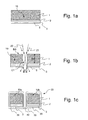
- Fig. 1a
- shows schematically a partially prepared coated tape in a cross-sectional view taken perpendicular to the direction of tape extension, in accordance with the invention;
- Fig. 1b
- shows the partially prepared coated tape of
Fig. 1 a during laser beam cutting, in accordance with the invention; - Fig. 1c
- shows the HTS coated tape resulting from the partially prepared coated tape of
Fig. 1b after deposition of a shunt layer; - Fig. 2a
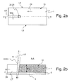
- shows a partially prepared coated tape, comprising a substrate, a buffer layer and a HTS layer, during laser beam cutting in accordance with the invention, in a top view;
- Fig. 2b
- shows schematically the partially prepared coated tape of
Fig. 2a in a cross-sectional view taken in parallel to the direction of tape extension; - Fig. 3a
- shows schematically a partially prepared coated tape in a cross-sectional view taken perpendicular to the direction of tape extension during laser beam cutting, wherein a metallic protection layer has been completely deposited before laser beam cutting, in accordance with the invention;
- Fig. 3b
- shows the HTS coated tape resulting from the partially prepared coated tape of
Fig. 3a after deposition of a shunt layer. - The invention presents a novel method for manufacturing of a HTS coated tape. It comprises a processing of a substrate tape, a deposition of at least one buffer layer, a deposition of a HTS film, a deposition of a metallic protection layer, a deposition of a metallic shunt layer, and a cutting of the tape in order to provide a desired tape form. The cutting of the tape is performed via a laser beam cutting. Later technique is typically applied together with a liquid flow directed along the laser beam and guiding this beam towards the tape. In accordance with the invention, the laser beam cutting is applied in between processing steps prior to the deposition of the metallic shunt layer.
-
Figs. 1 a through 1 c illustrate the steps of the inventive method by way of example. - On a
substrate tape 1, a buffer layer 2 (or alternatively several buffer layers) is deposited. On top of thebuffer layer 2, aHTS film 3 is deposited. Further, afirst part 5 of a metallic protection layer is deposited on top of theHTS film 3. A partly prepared HTS coatedtape 10 prepared in this way is illustrated inFig. 1a . - Then laser beam cutting is performed, compare
Fig. 1 b. For this purpose, alaser beam 22, which is focussed roughly at the center of the thickness TH of the substrate tape 10 (note that the thickness of thebuffer layer 2, theHTS film 3 and thepart 5 of the metallic protection layer is typically negligible as compared to TH), is directed onto the partially prepared coatedtape 10 from its side BS ("back side") facing away from thebuffer layer 2 and theHTS layer 3. Along thelaser beam 22, here aliquid flow 23 is directed into the cutting area. Thelaser beam 22 and theliquid flow 23 remove material from said cutting area, and a cut (or cutting gap) CT extending through the full thickness of the partially prepared coatedtape 10 results. The diameter of thelaser beam 22 in the cutting area roughly corresponds to the width WD of the cut CT. - After the laser beam cutting, the deposition of the metallic protection layer is continued; this deposition is here done such that a precious metal is deposited from every side ("around") onto the (here two)
parts tape 10, including sides facing the cut CT. In order to improve material deposition also in the cut CT, theparts parts metallic protection layer 35 completely covering theparts metallic shunt layer 36 is deposited, also completely covering the twoparts Fig. 1c , which shows the final HTS coated tape 20 (here comprising two parts, connected via an end side bridge 40). - In a preferred embodiment, the following materials/dimensions are employed: A Cr-Ni stainless steel tape, 4mm wide, 30m long and 0.1 mm thick, is used as a substrate tape. The buffer layer comprises two dielectric sub-layers: the first sub-layer is based on yttria stabilized zirconia (1.5 µm thick) which is bi-axially textured via alternating beam assisted deposition (compare
EP 1 693 905 B1 - The laser cutting in this example is based on using an YAG laser with a wavelength of 1.06µm, and an output power of 270 W. The partially prepared HTS coated tape was cut in longitudinal direction with a speed of 5 cm/sec provided via tape transportation. The water jet is installed here at 50 µm diameter.
- In an HTS coated tape manufactured as above described, the integral (entire) critical current of the superconducting element (i.e. in the HTS layer) was reduced only by 3%, as compared to 25-30% deterioration by using the prior art techniques doing a cutting after the deposition of the shunt layer.
- In more general cases, the cross-sectional dimension of the laser beam may be, in particular, between 1 and 500 µm (preferably from 10 to 100 µm). The laser may exhibit, in particular, a wavelength from 0.8 to 3 µm. The laser beam may be transported within liquid flow of different liquids such as water, ethyleneglycol, or alcohol. Liquid flow may be combined with a gas flow which may lead to further confinement of a cross-section of the laser beam in the cutting area. Laser methods based on double pulses, where the first pulse activates higher optical absorption of the surface, and the second pulse serves for the tape cutting, respectively, may be employed here as well.
- The partially prepared HTS coated tape is transported relative to the laser beam during the laser beam cutting. For short HTS coated tapes and/or for 2D laser beam cutting, the laser beam together with liquid and/or gas flows may be moved across the stationary HTS coated tape. In case of long (more than 10m) HTS coated tapes, preferably the tape is transported, and the laser beam as well as the liquid and/or gas flows are stationary or movable only to a limited extent (such as a up to 50cm).
- The relative transporting may be smooth, and typically with constant speed; transport is preferably an "in-plane" transport with respect to the tape (i.e. from left to right and up and down in the drawing plane of
Fig. 2a , see below); 1 D (linear) or 2D transport are possible. The transport and the laser cutting may be alternatively provided with at least one interruption; there may be a multitude of cutting interruptions during the processing if desired. - The substrate tapes applied in accordance with the invention are preferably made from an electrically conductive metal, such as stainless steel, typically sheeted to a thickness in the mm range or sub-mm range, thus offering some mechanical flexibility. The tape is, in general, much longer than wide (typically by a factor of at least 10; note that the production may be based on "endless" tape), and much wider than thick (typically by a factor of at least 10).
-
Figs. 2a (top view) and 2b (cross-sectional side view in the A-A plane, compare A-A line ofFig. 2a ) illustrate the progress of laser beam cutting in accordance with the invention. Thelaser beam 22 and aliquid flow 23 are here stationary, and the partially prepared coatedtape 10 is moved with a constant speed indirection 29 to the left in theFigs. 2a and 2b . Thelaser beam 22, with its laser beam direction LD is slightly tilted by an angle ϕ against the plane normal N of thetape 10 within the longitudinal A-A plane (comprising the said plane normal N and thedirection 29 of movement). ϕ is here about 10°, but other angles are also possible, with a preferred range of 5-30° for tilting angles in general. In the example shown, thelaser beam 22 is not tilted in a transversal plane (i.e. towards one of the long sides LS of the tape 10), though. - Further, in the example shown, the partially prepared coated
tape 10 only comprises asubstrate tape 1, abuffer layer 2 and aHTS layer 3, but no metallic protection layer so far; the latter will be deposited after the laser beam cutting is finished. The ratio R of the thickness TH of thesubstrate tape 1 and the width WD of the cut CT is here about R=4. -
Figs. 3a and 3b illustrate the inventive method in a further variant. In this variant, themetallic protection layer 35 has been completely deposited on thebuffer layer 2 before the laser beam cutting begins (note that the metallic protection layer is, in the example shown, only a planar surface protection). Accordingly, thelaser beam 22 also cuts through the completemetallic protection layer 35, compareFig. 3a . After the laser beam cutting, only themetallic shunt layer 36 has to be deposited still. The depositedmetallic shunt layer 36 here covers theparts tape 20 is shown inFig. 3 b.
Claims (15)
- A method for manufacturing of a high temperature superconductor (=HTS) coated tape (20), with the following steps:a) preparation of a substrate tape (1),b) deposition of at least one buffer layer (2),c) deposition of an HTS film (3),d) deposition of a metallic protection layer (35) on the HTS film (3),e) deposition of a metallic shunt layer (36),characterized in
that earlier than the deposition of the metallic shunt layer (36), the partially prepared coated tape (10) undergoes a laser beam cutting in order to provide a desired tape form,
wherein the laser beam cutting is applied together with a gas flow and/or a liquid flow (23). - Method according to claim 1, characterized in that a cross-sectional dimension of a laser beam (2) applied at the laser beam cutting is in between 1 and 500 µm, preferably in between 10 and 100 µm.
- Method according to one of the preceding claims, characterized in that the partially prepared coated tape (10) is transported during the laser beam cutting.
- Method according to one of the preceding claims, characterized in that a laser beam (22) applied during the laser beam cutting is tilted relative to the plane normal (N) of the partially prepared coated tape (10).
- Method according to claim 4, characterized in that the tilted laser beam (22) is provided in a plane (A-A) which is perpendicular to the surface of the partially prepared coated tape (10) and which contains the direction of the progress (29) of the laser beam (22) relative to the partially prepared coated tape (10) during laser beam cutting.
- Method according to any one of the preceding claims, characterized in that the laser beam cutting is performed later than the deposition of the at least one buffer layer (2),
in particular later than the deposition of the HTS layer (3). - Method according any one of the claims 1 through 6, characterized in that the laser beam cutting is done earlier than the deposition of the metallic protection layer (35).
- Method according to any one of the claims 1 through 6, characterized in that the deposition of the metallic protection layer (35) is performed in at least two steps, and that the laser beam cutting is performed in between the at least two steps of the deposition of the metallic protection layer (35).
- Method according to one of the preceding claims, characterized in that the manufacturing of the HTS coated tape (20) comprises at least one additional step of annealing, in particular in an oxygen atmosphere.
- Method according to claim 8 and 9, characterized in that the at least one annealing step is performed between or after the at least two steps of the deposition of the metallic protection layer (35).
- Method according to one of the preceding claim, characterized in that the laser beam cutting is done with an incidence of the laser beam (22) from the side (BS) of the partially prepared coated tape (10) which is opposite to the side where the at least one buffer layer (2) and the HTS film (3) are deposited.
- Method according to one of the preceding claims, characterized in that the deposition of the metallic protection layer (35) comprises a vacuum deposition process of a precious metal or precious metal alloy.
- Method according to one of the preceding claims, characterized in that the deposition of the metallic shunt layer (36) comprises galvanic plating.
- Method according to any one the preceding claims, characterized in that a ratio R of a thickness TH of the substrate tape (1) and a width WD of a cut (CT) of the partially prepared coated tape (10) caused by the laser beam cutting is in the range of R=0.5 to R=80.
- Method according to any one the preceding claims, characterized in that the gas flow and/or liquid flow (23) is chemically active with respect to the substrate tape (1).
Priority Applications (2)
| Application Number | Priority Date | Filing Date | Title |
|---|---|---|---|
| EP11154950.7A EP2490273B1 (en) | 2011-02-18 | 2011-02-18 | Method for manufacturing a HTS coated tape with laser beam cutting |
| US13/396,614 US8809236B2 (en) | 2011-02-18 | 2012-02-15 | Method for manufacturing a HTS coated tape with laser beam cutting |
Applications Claiming Priority (1)
| Application Number | Priority Date | Filing Date | Title |
|---|---|---|---|
| EP11154950.7A EP2490273B1 (en) | 2011-02-18 | 2011-02-18 | Method for manufacturing a HTS coated tape with laser beam cutting |
Publications (2)
| Publication Number | Publication Date |
|---|---|
| EP2490273A1 true EP2490273A1 (en) | 2012-08-22 |
| EP2490273B1 EP2490273B1 (en) | 2013-05-01 |
Family
ID=44168002
Family Applications (1)
| Application Number | Title | Priority Date | Filing Date |
|---|---|---|---|
| EP11154950.7A Not-in-force EP2490273B1 (en) | 2011-02-18 | 2011-02-18 | Method for manufacturing a HTS coated tape with laser beam cutting |
Country Status (2)
| Country | Link |
|---|---|
| US (1) | US8809236B2 (en) |
| EP (1) | EP2490273B1 (en) |
Cited By (3)
| Publication number | Priority date | Publication date | Assignee | Title |
|---|---|---|---|---|
| EP2991126A1 (en) | 2014-08-25 | 2016-03-02 | Theva Dünnschichttechnik GmbH | Method and device for producing a high temperature superconductor |
| EP3540795A1 (en) | 2018-03-15 | 2019-09-18 | Bruker HTS GmbH | A tape type superconductor with a plurality of elongated barrier structures |
| CN111347180A (en) * | 2020-03-27 | 2020-06-30 | 安徽汉超智能装备科技有限公司 | Buffering displacement mechanism of laser cutting machine |
Families Citing this family (10)
| Publication number | Priority date | Publication date | Assignee | Title |
|---|---|---|---|---|
| EP1132058A1 (en) * | 2000-03-06 | 2001-09-12 | Advanced Laser Applications Holding S.A. | Intravascular prothesis |
| JP6070403B2 (en) | 2013-05-13 | 2017-02-01 | トヨタ自動車株式会社 | Laser surface treatment method and laser surface treatment apparatus |
| KR101459583B1 (en) * | 2013-09-11 | 2014-11-10 | 주식회사 서남 | Superconductor and method for manufacturing the same |
| JP6853267B2 (en) | 2016-01-21 | 2021-03-31 | ブルックヘイブン テクノロジー グループ, インコーポレイテッド | 2nd generation superconducting filaments and cables |
| KR102179595B1 (en) | 2016-09-07 | 2020-11-16 | 브룩해븐 테크놀로지 그룹, 인크. | Reel-to-reel peeling and processing of second-generation superconductors |
| EP3635754B1 (en) | 2017-06-09 | 2024-11-27 | Brookhaven Technology Group, Inc. | Flexible multi-filament high temperature superconducting cable |
| JP2019139883A (en) * | 2018-02-07 | 2019-08-22 | 住友電気工業株式会社 | Superconducting wire rod, superconducting cable, and method for manufacturing superconducting wire rod |
| JP2023508619A (en) * | 2019-02-18 | 2023-03-03 | スーパーパワー インコーポレイテッド | Manufacturing method of superconducting wire |
| US12412681B2 (en) * | 2020-02-24 | 2025-09-09 | University Of Houston System | Hybrid round superconductor wires using Nb—Ti filaments |
| JPWO2025033130A1 (en) * | 2023-08-09 | 2025-02-13 |
Citations (12)
| Publication number | Priority date | Publication date | Assignee | Title |
|---|---|---|---|---|
| EP0375578A1 (en) | 1988-12-21 | 1990-06-27 | LASER MEDICAL TECHNOLOGY, Inc. | Device for the cutting or vaporizing of material and different substances by using the laser effect |
| GB2229125A (en) * | 1989-01-09 | 1990-09-19 | Mitsubishi Electric Corp | Laser beam machine |
| DE4418845C1 (en) | 1994-05-30 | 1995-09-28 | Bernold Richerzhagen | Method and appts. for laser beam treatment of materials |
| US20030129814A1 (en) | 2002-01-08 | 2003-07-10 | Fujitsu Limited | Method of manufacturing semiconductor device |
| WO2005096322A1 (en) * | 2004-03-31 | 2005-10-13 | Industrial Research Limited | Composite superconductor cable produced by transposing planar subconductors |
| US20070179063A1 (en) * | 2006-01-10 | 2007-08-02 | American Superconductor Corporation | Fabrication of sealed high temperature superconductor wires |
| US20070228025A1 (en) * | 2004-09-04 | 2007-10-04 | Trumpf Werkzeugmaschinen Gmbh + Co. Kg | Determining the relative positions of the axes of a laser machining beam and a process gas jet |
| US20070278195A1 (en) | 2004-11-10 | 2007-12-06 | Synova Sa | Method and Device for Generating a Jet of Fluid for Material Processing and Fluid Nozzle for Use in Said Device |
| US20080113870A1 (en) | 2006-11-10 | 2008-05-15 | Korea Polytechnic University | Method for fabricating filament type high-temperature superconducting wire |
| EP1693905B1 (en) | 2005-02-17 | 2008-08-20 | European High Temperature Superconductors GmbH & Co. KG | Process of manufacturing biaxial oriented coatings |
| US7728258B2 (en) | 2004-05-19 | 2010-06-01 | Synova Sa | Laser machining of a workpiece |
| US7774035B2 (en) | 2003-06-27 | 2010-08-10 | Superpower, Inc. | Superconducting articles having dual sided structures |
Family Cites Families (2)
| Publication number | Priority date | Publication date | Assignee | Title |
|---|---|---|---|---|
| US8093532B2 (en) * | 2008-03-31 | 2012-01-10 | Electro Scientific Industries, Inc. | Laser machining of fired ceramic and other hard and/or thick materials |
| EP2490272B1 (en) * | 2011-02-18 | 2013-08-21 | Bruker HTS GmbH | Superconducting element with elongated opening and method for manufacturing the same |
-
2011
- 2011-02-18 EP EP11154950.7A patent/EP2490273B1/en not_active Not-in-force
-
2012
- 2012-02-15 US US13/396,614 patent/US8809236B2/en not_active Expired - Fee Related
Patent Citations (12)
| Publication number | Priority date | Publication date | Assignee | Title |
|---|---|---|---|---|
| EP0375578A1 (en) | 1988-12-21 | 1990-06-27 | LASER MEDICAL TECHNOLOGY, Inc. | Device for the cutting or vaporizing of material and different substances by using the laser effect |
| GB2229125A (en) * | 1989-01-09 | 1990-09-19 | Mitsubishi Electric Corp | Laser beam machine |
| DE4418845C1 (en) | 1994-05-30 | 1995-09-28 | Bernold Richerzhagen | Method and appts. for laser beam treatment of materials |
| US20030129814A1 (en) | 2002-01-08 | 2003-07-10 | Fujitsu Limited | Method of manufacturing semiconductor device |
| US7774035B2 (en) | 2003-06-27 | 2010-08-10 | Superpower, Inc. | Superconducting articles having dual sided structures |
| WO2005096322A1 (en) * | 2004-03-31 | 2005-10-13 | Industrial Research Limited | Composite superconductor cable produced by transposing planar subconductors |
| US7728258B2 (en) | 2004-05-19 | 2010-06-01 | Synova Sa | Laser machining of a workpiece |
| US20070228025A1 (en) * | 2004-09-04 | 2007-10-04 | Trumpf Werkzeugmaschinen Gmbh + Co. Kg | Determining the relative positions of the axes of a laser machining beam and a process gas jet |
| US20070278195A1 (en) | 2004-11-10 | 2007-12-06 | Synova Sa | Method and Device for Generating a Jet of Fluid for Material Processing and Fluid Nozzle for Use in Said Device |
| EP1693905B1 (en) | 2005-02-17 | 2008-08-20 | European High Temperature Superconductors GmbH & Co. KG | Process of manufacturing biaxial oriented coatings |
| US20070179063A1 (en) * | 2006-01-10 | 2007-08-02 | American Superconductor Corporation | Fabrication of sealed high temperature superconductor wires |
| US20080113870A1 (en) | 2006-11-10 | 2008-05-15 | Korea Polytechnic University | Method for fabricating filament type high-temperature superconducting wire |
Cited By (3)
| Publication number | Priority date | Publication date | Assignee | Title |
|---|---|---|---|---|
| EP2991126A1 (en) | 2014-08-25 | 2016-03-02 | Theva Dünnschichttechnik GmbH | Method and device for producing a high temperature superconductor |
| EP3540795A1 (en) | 2018-03-15 | 2019-09-18 | Bruker HTS GmbH | A tape type superconductor with a plurality of elongated barrier structures |
| CN111347180A (en) * | 2020-03-27 | 2020-06-30 | 安徽汉超智能装备科技有限公司 | Buffering displacement mechanism of laser cutting machine |
Also Published As
| Publication number | Publication date |
|---|---|
| US8809236B2 (en) | 2014-08-19 |
| EP2490273B1 (en) | 2013-05-01 |
| US20120211475A1 (en) | 2012-08-23 |
Similar Documents
| Publication | Publication Date | Title |
|---|---|---|
| EP2490273B1 (en) | Method for manufacturing a HTS coated tape with laser beam cutting | |
| EP3133612B1 (en) | Oxide superconducting wire material and oxide superconducting wire material production method | |
| EP3622565B1 (en) | Laminated high temperature superconducting wires having increased engineering current densities | |
| CN114144850B (en) | Manufacturing of superconducting wire | |
| EP2495735A1 (en) | Low ac-loss multi-filament type superconductive wire material, and manufacturing method thereof | |
| JP5367927B1 (en) | Superconducting film-forming substrate, superconducting wire, and method of manufacturing superconducting wire | |
| EP2490272B1 (en) | Superconducting element with elongated opening and method for manufacturing the same | |
| KR20240162044A (en) | Superconducting wires and superconducting devices | |
| EP3367394A1 (en) | Oxide superconducting wire | |
| EP3007180B1 (en) | Oxide superconductor and method for manufacturing the same | |
| CN104221097A (en) | Oxide superconducting wire having reinforcing materials | |
| JP5727278B2 (en) | Manufacturing method of oxide superconducting thin film wire | |
| EP2453447A1 (en) | Substrate, method of producing substrate superconducting wire and method of producing of superconducting wire | |
| EP1668712B1 (en) | Superconductive composite tape and corresponding method of fabrication | |
| Wulff et al. | A two-level undercut-profile substrate for chemical-solution-based filamentary coated conductors | |
| KR101593101B1 (en) | ceramic wire, manufacturing method, and manufacturing apparatus of the same | |
| Miyata et al. | Long and high rate production of IBAD templates for YBCO coated conductors | |
| EP3696826A1 (en) | Connection structure for oxide superconducting wire materials | |
| JP2017152210A (en) | Oxide superconducting wire and method for producing the same | |
| JP2011113664A (en) | Superconducting thin film wire-manufacturing method | |
| EP4283635B1 (en) | High-temperature superconducting coated conductor and method for manufacturing same | |
| JP2013012407A (en) | Method of manufacturing oxide superconducting thin film wire rod | |
| JP6492205B2 (en) | Manufacturing method of oxide superconducting wire | |
| KR20240164881A (en) | Superconducting wires and superconducting devices | |
| KR20240053041A (en) | superconducting wire |
Legal Events
| Date | Code | Title | Description |
|---|---|---|---|
| PUAI | Public reference made under article 153(3) epc to a published international application that has entered the european phase |
Free format text: ORIGINAL CODE: 0009012 |
|
| 17P | Request for examination filed |
Effective date: 20111119 |
|
| AK | Designated contracting states |
Kind code of ref document: A1 Designated state(s): AL AT BE BG CH CY CZ DE DK EE ES FI FR GB GR HR HU IE IS IT LI LT LU LV MC MK MT NL NO PL PT RO RS SE SI SK SM TR |
|
| AX | Request for extension of the european patent |
Extension state: BA ME |
|
| GRAP | Despatch of communication of intention to grant a patent |
Free format text: ORIGINAL CODE: EPIDOSNIGR1 |
|
| GRAS | Grant fee paid |
Free format text: ORIGINAL CODE: EPIDOSNIGR3 |
|
| GRAA | (expected) grant |
Free format text: ORIGINAL CODE: 0009210 |
|
| AK | Designated contracting states |
Kind code of ref document: B1 Designated state(s): AL AT BE BG CH CY CZ DE DK EE ES FI FR GB GR HR HU IE IS IT LI LT LU LV MC MK MT NL NO PL PT RO RS SE SI SK SM TR |
|
| REG | Reference to a national code |
Ref country code: GB Ref legal event code: FG4D |
|
| REG | Reference to a national code |
Ref country code: AT Ref legal event code: REF Ref document number: 610401 Country of ref document: AT Kind code of ref document: T Effective date: 20130515 Ref country code: CH Ref legal event code: EP |
|
| REG | Reference to a national code |
Ref country code: IE Ref legal event code: FG4D |
|
| REG | Reference to a national code |
Ref country code: DE Ref legal event code: R096 Ref document number: 602011001488 Country of ref document: DE Effective date: 20130704 |
|
| REG | Reference to a national code |
Ref country code: NL Ref legal event code: VDEP Effective date: 20130501 |
|
| REG | Reference to a national code |
Ref country code: LT Ref legal event code: MG4D |
|
| PG25 | Lapsed in a contracting state [announced via postgrant information from national office to epo] |
Ref country code: SI Free format text: LAPSE BECAUSE OF FAILURE TO SUBMIT A TRANSLATION OF THE DESCRIPTION OR TO PAY THE FEE WITHIN THE PRESCRIBED TIME-LIMIT Effective date: 20130501 Ref country code: GR Free format text: LAPSE BECAUSE OF FAILURE TO SUBMIT A TRANSLATION OF THE DESCRIPTION OR TO PAY THE FEE WITHIN THE PRESCRIBED TIME-LIMIT Effective date: 20130802 Ref country code: FI Free format text: LAPSE BECAUSE OF FAILURE TO SUBMIT A TRANSLATION OF THE DESCRIPTION OR TO PAY THE FEE WITHIN THE PRESCRIBED TIME-LIMIT Effective date: 20130501 Ref country code: IS Free format text: LAPSE BECAUSE OF FAILURE TO SUBMIT A TRANSLATION OF THE DESCRIPTION OR TO PAY THE FEE WITHIN THE PRESCRIBED TIME-LIMIT Effective date: 20130901 Ref country code: NO Free format text: LAPSE BECAUSE OF FAILURE TO SUBMIT A TRANSLATION OF THE DESCRIPTION OR TO PAY THE FEE WITHIN THE PRESCRIBED TIME-LIMIT Effective date: 20130801 Ref country code: PT Free format text: LAPSE BECAUSE OF FAILURE TO SUBMIT A TRANSLATION OF THE DESCRIPTION OR TO PAY THE FEE WITHIN THE PRESCRIBED TIME-LIMIT Effective date: 20130902 Ref country code: LT Free format text: LAPSE BECAUSE OF FAILURE TO SUBMIT A TRANSLATION OF THE DESCRIPTION OR TO PAY THE FEE WITHIN THE PRESCRIBED TIME-LIMIT Effective date: 20130501 Ref country code: SE Free format text: LAPSE BECAUSE OF FAILURE TO SUBMIT A TRANSLATION OF THE DESCRIPTION OR TO PAY THE FEE WITHIN THE PRESCRIBED TIME-LIMIT Effective date: 20130501 Ref country code: ES Free format text: LAPSE BECAUSE OF FAILURE TO SUBMIT A TRANSLATION OF THE DESCRIPTION OR TO PAY THE FEE WITHIN THE PRESCRIBED TIME-LIMIT Effective date: 20130812 |
|
| PG25 | Lapsed in a contracting state [announced via postgrant information from national office to epo] |
Ref country code: PL Free format text: LAPSE BECAUSE OF FAILURE TO SUBMIT A TRANSLATION OF THE DESCRIPTION OR TO PAY THE FEE WITHIN THE PRESCRIBED TIME-LIMIT Effective date: 20130501 Ref country code: RS Free format text: LAPSE BECAUSE OF FAILURE TO SUBMIT A TRANSLATION OF THE DESCRIPTION OR TO PAY THE FEE WITHIN THE PRESCRIBED TIME-LIMIT Effective date: 20130501 Ref country code: BG Free format text: LAPSE BECAUSE OF FAILURE TO SUBMIT A TRANSLATION OF THE DESCRIPTION OR TO PAY THE FEE WITHIN THE PRESCRIBED TIME-LIMIT Effective date: 20130801 Ref country code: HR Free format text: LAPSE BECAUSE OF FAILURE TO SUBMIT A TRANSLATION OF THE DESCRIPTION OR TO PAY THE FEE WITHIN THE PRESCRIBED TIME-LIMIT Effective date: 20130501 Ref country code: CY Free format text: LAPSE BECAUSE OF FAILURE TO SUBMIT A TRANSLATION OF THE DESCRIPTION OR TO PAY THE FEE WITHIN THE PRESCRIBED TIME-LIMIT Effective date: 20130501 |
|
| PG25 | Lapsed in a contracting state [announced via postgrant information from national office to epo] |
Ref country code: LV Free format text: LAPSE BECAUSE OF FAILURE TO SUBMIT A TRANSLATION OF THE DESCRIPTION OR TO PAY THE FEE WITHIN THE PRESCRIBED TIME-LIMIT Effective date: 20130501 |
|
| PG25 | Lapsed in a contracting state [announced via postgrant information from national office to epo] |
Ref country code: CZ Free format text: LAPSE BECAUSE OF FAILURE TO SUBMIT A TRANSLATION OF THE DESCRIPTION OR TO PAY THE FEE WITHIN THE PRESCRIBED TIME-LIMIT Effective date: 20130501 Ref country code: SK Free format text: LAPSE BECAUSE OF FAILURE TO SUBMIT A TRANSLATION OF THE DESCRIPTION OR TO PAY THE FEE WITHIN THE PRESCRIBED TIME-LIMIT Effective date: 20130501 Ref country code: EE Free format text: LAPSE BECAUSE OF FAILURE TO SUBMIT A TRANSLATION OF THE DESCRIPTION OR TO PAY THE FEE WITHIN THE PRESCRIBED TIME-LIMIT Effective date: 20130501 Ref country code: BE Free format text: LAPSE BECAUSE OF FAILURE TO SUBMIT A TRANSLATION OF THE DESCRIPTION OR TO PAY THE FEE WITHIN THE PRESCRIBED TIME-LIMIT Effective date: 20130501 Ref country code: DK Free format text: LAPSE BECAUSE OF FAILURE TO SUBMIT A TRANSLATION OF THE DESCRIPTION OR TO PAY THE FEE WITHIN THE PRESCRIBED TIME-LIMIT Effective date: 20130501 |
|
| PG25 | Lapsed in a contracting state [announced via postgrant information from national office to epo] |
Ref country code: NL Free format text: LAPSE BECAUSE OF FAILURE TO SUBMIT A TRANSLATION OF THE DESCRIPTION OR TO PAY THE FEE WITHIN THE PRESCRIBED TIME-LIMIT Effective date: 20130501 Ref country code: IT Free format text: LAPSE BECAUSE OF FAILURE TO SUBMIT A TRANSLATION OF THE DESCRIPTION OR TO PAY THE FEE WITHIN THE PRESCRIBED TIME-LIMIT Effective date: 20130501 Ref country code: RO Free format text: LAPSE BECAUSE OF FAILURE TO SUBMIT A TRANSLATION OF THE DESCRIPTION OR TO PAY THE FEE WITHIN THE PRESCRIBED TIME-LIMIT Effective date: 20130501 |
|
| PLBE | No opposition filed within time limit |
Free format text: ORIGINAL CODE: 0009261 |
|
| STAA | Information on the status of an ep patent application or granted ep patent |
Free format text: STATUS: NO OPPOSITION FILED WITHIN TIME LIMIT |
|
| 26N | No opposition filed |
Effective date: 20140204 |
|
| REG | Reference to a national code |
Ref country code: DE Ref legal event code: R097 Ref document number: 602011001488 Country of ref document: DE Effective date: 20140204 |
|
| PG25 | Lapsed in a contracting state [announced via postgrant information from national office to epo] |
Ref country code: LU Free format text: LAPSE BECAUSE OF FAILURE TO SUBMIT A TRANSLATION OF THE DESCRIPTION OR TO PAY THE FEE WITHIN THE PRESCRIBED TIME-LIMIT Effective date: 20140218 Ref country code: MC Free format text: LAPSE BECAUSE OF FAILURE TO SUBMIT A TRANSLATION OF THE DESCRIPTION OR TO PAY THE FEE WITHIN THE PRESCRIBED TIME-LIMIT Effective date: 20130501 |
|
| REG | Reference to a national code |
Ref country code: IE Ref legal event code: MM4A |
|
| PG25 | Lapsed in a contracting state [announced via postgrant information from national office to epo] |
Ref country code: IE Free format text: LAPSE BECAUSE OF NON-PAYMENT OF DUE FEES Effective date: 20140218 |
|
| REG | Reference to a national code |
Ref country code: FR Ref legal event code: PLFP Year of fee payment: 6 |
|
| PG25 | Lapsed in a contracting state [announced via postgrant information from national office to epo] |
Ref country code: MT Free format text: LAPSE BECAUSE OF FAILURE TO SUBMIT A TRANSLATION OF THE DESCRIPTION OR TO PAY THE FEE WITHIN THE PRESCRIBED TIME-LIMIT Effective date: 20130501 |
|
| PG25 | Lapsed in a contracting state [announced via postgrant information from national office to epo] |
Ref country code: SM Free format text: LAPSE BECAUSE OF FAILURE TO SUBMIT A TRANSLATION OF THE DESCRIPTION OR TO PAY THE FEE WITHIN THE PRESCRIBED TIME-LIMIT Effective date: 20130501 |
|
| PG25 | Lapsed in a contracting state [announced via postgrant information from national office to epo] |
Ref country code: TR Free format text: LAPSE BECAUSE OF FAILURE TO SUBMIT A TRANSLATION OF THE DESCRIPTION OR TO PAY THE FEE WITHIN THE PRESCRIBED TIME-LIMIT Effective date: 20130501 Ref country code: HU Free format text: LAPSE BECAUSE OF FAILURE TO SUBMIT A TRANSLATION OF THE DESCRIPTION OR TO PAY THE FEE WITHIN THE PRESCRIBED TIME-LIMIT; INVALID AB INITIO Effective date: 20110218 |
|
| REG | Reference to a national code |
Ref country code: FR Ref legal event code: PLFP Year of fee payment: 7 |
|
| REG | Reference to a national code |
Ref country code: FR Ref legal event code: PLFP Year of fee payment: 8 |
|
| PG25 | Lapsed in a contracting state [announced via postgrant information from national office to epo] |
Ref country code: MK Free format text: LAPSE BECAUSE OF FAILURE TO SUBMIT A TRANSLATION OF THE DESCRIPTION OR TO PAY THE FEE WITHIN THE PRESCRIBED TIME-LIMIT Effective date: 20130501 |
|
| PG25 | Lapsed in a contracting state [announced via postgrant information from national office to epo] |
Ref country code: AL Free format text: LAPSE BECAUSE OF FAILURE TO SUBMIT A TRANSLATION OF THE DESCRIPTION OR TO PAY THE FEE WITHIN THE PRESCRIBED TIME-LIMIT Effective date: 20130501 |
|
| PGFP | Annual fee paid to national office [announced via postgrant information from national office to epo] |
Ref country code: AT Payment date: 20200218 Year of fee payment: 10 Ref country code: DE Payment date: 20200220 Year of fee payment: 10 Ref country code: GB Payment date: 20200225 Year of fee payment: 10 |
|
| PGFP | Annual fee paid to national office [announced via postgrant information from national office to epo] |
Ref country code: CH Payment date: 20200224 Year of fee payment: 10 |
|
| PGFP | Annual fee paid to national office [announced via postgrant information from national office to epo] |
Ref country code: FR Payment date: 20200220 Year of fee payment: 10 |
|
| REG | Reference to a national code |
Ref country code: DE Ref legal event code: R119 Ref document number: 602011001488 Country of ref document: DE |
|
| REG | Reference to a national code |
Ref country code: AT Ref legal event code: MM01 Ref document number: 610401 Country of ref document: AT Kind code of ref document: T Effective date: 20210218 |
|
| GBPC | Gb: european patent ceased through non-payment of renewal fee |
Effective date: 20210218 |
|
| PG25 | Lapsed in a contracting state [announced via postgrant information from national office to epo] |
Ref country code: CH Free format text: LAPSE BECAUSE OF NON-PAYMENT OF DUE FEES Effective date: 20210228 Ref country code: AT Free format text: LAPSE BECAUSE OF NON-PAYMENT OF DUE FEES Effective date: 20210218 Ref country code: LI Free format text: LAPSE BECAUSE OF NON-PAYMENT OF DUE FEES Effective date: 20210228 |
|
| PG25 | Lapsed in a contracting state [announced via postgrant information from national office to epo] |
Ref country code: FR Free format text: LAPSE BECAUSE OF NON-PAYMENT OF DUE FEES Effective date: 20210228 Ref country code: GB Free format text: LAPSE BECAUSE OF NON-PAYMENT OF DUE FEES Effective date: 20210218 Ref country code: DE Free format text: LAPSE BECAUSE OF NON-PAYMENT OF DUE FEES Effective date: 20210901 |