EP2495863B1 - Réduction CMV sous des conditions transitoires de BUS - Google Patents
Réduction CMV sous des conditions transitoires de BUS Download PDFInfo
- Publication number
- EP2495863B1 EP2495863B1 EP12155964.5A EP12155964A EP2495863B1 EP 2495863 B1 EP2495863 B1 EP 2495863B1 EP 12155964 A EP12155964 A EP 12155964A EP 2495863 B1 EP2495863 B1 EP 2495863B1
- Authority
- EP
- European Patent Office
- Prior art keywords
- rectifier
- phase
- mode
- input
- phases
- Prior art date
- Legal status (The legal status is an assumption and is not a legal conclusion. Google has not performed a legal analysis and makes no representation as to the accuracy of the status listed.)
- Not-in-force
Links
Images


Classifications
-
- H—ELECTRICITY
- H02—GENERATION; CONVERSION OR DISTRIBUTION OF ELECTRIC POWER
- H02M—APPARATUS FOR CONVERSION BETWEEN AC AND AC, BETWEEN AC AND DC, OR BETWEEN DC AND DC, AND FOR USE WITH MAINS OR SIMILAR POWER SUPPLY SYSTEMS; CONVERSION OF DC OR AC INPUT POWER INTO SURGE OUTPUT POWER; CONTROL OR REGULATION THEREOF
- H02M5/00—Conversion of AC power input into AC power output, e.g. for change of voltage, for change of frequency, for change of number of phases
- H02M5/40—Conversion of AC power input into AC power output, e.g. for change of voltage, for change of frequency, for change of number of phases with intermediate conversion into DC
- H02M5/42—Conversion of AC power input into AC power output, e.g. for change of voltage, for change of frequency, for change of number of phases with intermediate conversion into DC by static converters
- H02M5/44—Conversion of AC power input into AC power output, e.g. for change of voltage, for change of frequency, for change of number of phases with intermediate conversion into DC by static converters using discharge tubes or semiconductor devices to convert the intermediate DC into AC
- H02M5/453—Conversion of AC power input into AC power output, e.g. for change of voltage, for change of frequency, for change of number of phases with intermediate conversion into DC by static converters using discharge tubes or semiconductor devices to convert the intermediate DC into AC using devices of a triode or transistor type requiring continuous application of a control signal
- H02M5/458—Conversion of AC power input into AC power output, e.g. for change of voltage, for change of frequency, for change of number of phases with intermediate conversion into DC by static converters using discharge tubes or semiconductor devices to convert the intermediate DC into AC using devices of a triode or transistor type requiring continuous application of a control signal using semiconductor devices only
- H02M5/4585—Conversion of AC power input into AC power output, e.g. for change of voltage, for change of frequency, for change of number of phases with intermediate conversion into DC by static converters using discharge tubes or semiconductor devices to convert the intermediate DC into AC using devices of a triode or transistor type requiring continuous application of a control signal using semiconductor devices only having a rectifier with controlled elements
-
- H—ELECTRICITY
- H02—GENERATION; CONVERSION OR DISTRIBUTION OF ELECTRIC POWER
- H02P—CONTROL OR REGULATION OF ELECTRIC MOTORS, ELECTRIC GENERATORS OR DYNAMO-ELECTRIC CONVERTERS; CONTROLLING TRANSFORMERS, REACTORS OR CHOKE COILS
- H02P27/00—Arrangements or methods for the control of AC motors characterised by the kind of supply voltage
- H02P27/04—Arrangements or methods for the control of AC motors characterised by the kind of supply voltage using variable-frequency supply voltage, e.g. inverter or converter supply voltage
- H02P27/06—Arrangements or methods for the control of AC motors characterised by the kind of supply voltage using variable-frequency supply voltage, e.g. inverter or converter supply voltage using DC to AC converters or inverters
-
- H—ELECTRICITY
- H02—GENERATION; CONVERSION OR DISTRIBUTION OF ELECTRIC POWER
- H02P—CONTROL OR REGULATION OF ELECTRIC MOTORS, ELECTRIC GENERATORS OR DYNAMO-ELECTRIC CONVERTERS; CONTROLLING TRANSFORMERS, REACTORS OR CHOKE COILS
- H02P29/00—Arrangements for regulating or controlling electric motors, appropriate for both AC and DC motors
- H02P29/02—Providing protection against overload without automatic interruption of supply
- H02P29/024—Detecting a fault condition, e.g. short circuit, locked rotor, open circuit or loss of load
- H02P29/0241—Detecting a fault condition, e.g. short circuit, locked rotor, open circuit or loss of load the fault being an overvoltage
-
- H—ELECTRICITY
- H02—GENERATION; CONVERSION OR DISTRIBUTION OF ELECTRIC POWER
- H02P—CONTROL OR REGULATION OF ELECTRIC MOTORS, ELECTRIC GENERATORS OR DYNAMO-ELECTRIC CONVERTERS; CONTROLLING TRANSFORMERS, REACTORS OR CHOKE COILS
- H02P2201/00—Indexing scheme relating to controlling arrangements characterised by the converter used
- H02P2201/13—DC-link of current link type, e.g. typically for thyristor bridges, having an inductor in series with rectifier
Definitions
- the present invention relates generally to electrical power conversion and more particularly to apparatus and methods for reducing common mode voltage stresses for current source converter-based drive systems.
- Motor drives are electric power conversion systems that convert input power from a line-side source to a different form to provide controlled drive currents to the windings of a load, such as an electric motor.
- Current source converter (CSC) type drives typically include a switching rectifier with AC input power being selectively switched to create a DC link current that is fed to an output inverter which creates single or multi-phase AC output current for driving a motor load at a controlled speed and torque. Both the AC to DC and DC to AC portions of the motor drive often use solid state switching components.
- transformerless voltage source and current source inverters VSI/CSI
- Common mode currents and voltages can also stress drive system components, such as internal link chokes or other components.
- the peak common-mode voltage can equal the peak line-to-neutral output voltage during bus transient conditions, which can double the line-to-ground voltage on the motor. Accordingly, there is a need for an improved systems and method for reducing common mode voltage stresses in motor drives, especially during bus transients in the drive system, for example, to prevent component failures or premature degradation.
- US2008/0013348 (A1 ) describes a protection scheme to protect pulse width modulated drives.
- the semiconductor devices of the drive are protected from transient signals such as power line spikes and loss of line.
- the scheme uses an adaptive technique to determine the normal or steady state distortion by transients or harmonics in an unfiltered power signal.
- the present distortion value is compared to the normal distortion. If the present distortion exceeds the steady state value by a given amount, then the drive is placed in freewheel mode to protect the semiconductor devices in the drive.
- a freewheel mode is one where both of a series connected devices are conducting.
- EP2031746 (A1 ) describes a method to control the phase and magnitude of an input current command vector of a virtual input converter to control the magnitude of a virtual DC voltage.
- An intermediate voltage between input lines and a zero voltage vector is used in the region where the input current command vector is at a low output voltage, and the maximum voltage between the input lines and the intermediate voltage between the input lines is used in the high output voltage region.
- a PWM control is performed in a virtual output inverter to reduce a number of divisions in one operation period of duty pulses.
- the output voltage is controlled in the low output voltage region by using an intermediate voltage between the input lines.
- the virtual direct current voltage is at an ideally maximum constant, and the PWM control is made in the virtual output inverter.
- the switching pattern is determined by using the zero-voltage vector mode connected to the input intermediate phase in order to reduce the common mode voltage which gives ill influence on equipment.
- USRE38439 (E) describes a DC matrix converter having six forward current conducting power switches and six reverse current conducting power switches.
- the switch-on time of DC matrix power switches is determined by the ratio of an instantaneous voltage command signal, V*, to the instantaneous magnitude, V, of the three-phase AC mains in stationary dq coordinates, along with the phase relationship between the present instantaneous phase of said AC mains voltage in stationary dq coordinates and the leading and lagging boundaries of six phase sectors that span a cycle of said AC mains.
- Zero vectors defined as the short circuiting of output terminals by a set of like-phase switches, are selected to minimize the common mode voltage.
- the peak common-mode voltage produced by a zero vector can be reduced by half by restricting its usage during the AC cycle. To realize this reduction factor over the entire AC cycle, similar restrictions are placed on the other zero vectors.
- a power conversion system which includes an active rectifier, an inverter for driving a motor or other load, and a switch control system having a rectifier control and a bus transient control component coupled to the rectifier control.
- the switching control system provides switching control signals in a first mode for normal operation and in a second mode for protective operation.
- the rectifier controls the amount of current provided in accordance with a desired value set by the inverter demands.
- the bus transient control is activated in the second mode based on a detected or sensed distortion of steady state condition is present at power conversion system, such as according to at least one feedback signal or value from a feedback circuit.
- the bus transient control causes the rectifier control to bypass a selected phase circuit, such as a rectifier phase, during the second mode to regulate the current based at least partially on a selection criterion.
- the phase bypassed is selected at any given time based at least partially on absolute voltage values at the AC input nodes.
- the bypass phase is selected as that for which the associated absolute line-to-neutral voltage value is smallest (e.g., closest to zero).
- the selected phase is that which is not associated with phases having the highest absolute line-to-line voltage value.
- This selection may change based on the absolute voltages during the operation in the second mode, and the bus transient controller in certain embodiments determines the selected phase so as to bypass each phase in a sequential pattern, where the selected phases, such as in the system's rectifier, are bypassed by shorting switching devices in the selected phase while switching devices of other phases are opened.
- a method for operating a power conversion system.
- the method involves two operational modes of a power drive.
- rectifier switching control signals are provided to an active rectifier to convert input power to provide a DC current, such as to an intermediate DC circuit, and the DC current is regulated.
- the method further includes monitoring for a transient condition, and upon detection of a transient, operating in a second operational mode by bypassing a selected rectifier phase to reduce a common mode voltage between an AC input and the AC output. Certain embodiments include shorting the rectifier phases in a sequential pattern in the second mode.
- the bypassed rectifier phase is selected based on an absolute voltage value by shorting the selected rectifier phase not associated with AC input nodes having the highest absolute line-to-line voltage.
- Certain embodiments include bypassing the rectifier phase having a minimum absolute line-to-neutral voltage value.
- the method in certain embodiments further includes sensing the transient condition of at least one of the rectifier, the intermediate DC circuit, and the inverter, as well as setting the operational mode of the motor drive to the second mode according to the sensed transient condition.
- the drive 110 is a current source converter (CSC) type, with an input 112 connected to the AC power source 111. While illustrated as having a three phase input 112, other embodiments may provide a single phase AC input or may include a multiphase input adapted to receive three or more input phases.
- CSC current source converter
- Other power conversion systems are also envisioned with dual bridge matrix drives, indirect matrix drives or matrix drives that include a matrix of switches that control an AC input power at an AC input node to an AC output node.
- the CSC drive 110 provides variable frequency, variable amplitude single or multiphase AC output power at output terminals 114 to drive an AC motor load 120, which has three phase windings in the illustrated example.
- the output 114 in other embodiments may provide a single phase AC output or may be of any number of phases.
- the motor drive 110 includes an intermediate DC circuit 150 with a DC link choke having upper and lower windings, WA and WB, coupled between an input rectifier 110a and an output inverter 110b comprises switching devices therein.
- the DC link could be a simple DC link inductor or a common mode choke as in the illustrated example.
- the illustrated drive 110 moreover, provides input filtering including inductors Li in each input phase and input filter capacitors Ci coupled between the input lines A, B, C, and an input neutral node respectively thereat.
- the rectifier 110a is a current source rectifier (CSR), for example, that is coupled with the output inverter 110b by the intermediate DC circuit 150, and one or more isolation components (e.g., transformers, not shown) may optionally be included in the drive 110.
- CSR current source rectifier
- the output inverter 110b is a current source inverter (CSI), for example, that is adapted to receive the DC output of the DC circuit 150 for generating an AC output at the output 114, which provides output electrical power to the motor load 120 via lines U, V, and W, and includes output capacitors Cm coupled between the load 120 and an output neutral node.
- CSI current source inverter
- the active rectifier 110a includes a plurality of phases/phase circuits or leg stages that have an arrangement of switching devices S1-S6 coupled between the input 112 and the DC circuit 150 and operates according to a plurality of rectifier switching control signals 142a provided by a rectifier control component 144a of a switch control system 140.
- the phases include a first phase 121, a second phase 123 and a third phase 125, for example, having switching devices respectively therein.
- the rectifier 110a is not limited by the number of phase arrangements therein and may include one more phase arrangements that include other switching devices for a current flow.
- the first, the second and the third phases 121, 123, and 125 have a pair of switching devices respectively that are connected in a series arrangement.
- the AC input power is switched by the rectifier switches S1-S6 of each phase to create an intermediate DC bus current Idc in the intermediate circuit 150.
- the inverter 110b includes switching devices S7-S12 of phases therein coupled with the DC circuit 150 and the output 114, which operate according to corresponding switching control signals 142b.
- An inverter control component 144b of the switch control system 140 provides the switching control signals 142b to selectively convert DC power from the DC circuit 150 to provide the AC output power to drive the motor load 120.
- a feedback circuit 118 senses transients at the grid input, such as harmonics and background distortion, in the power signals and based on the sensed a transient condition that places the drive in a protection mode/state to prevent damage to any components.
- the voltage in certain implementations can be measured (e.g., line-to-neutral) at the capacitors Ci at the grid side filter circuit 112 vie the feedback system 118 for line side transient control, where a common cause of the bus transient is grid-side ground faults, PFC capacitor switching, etc.
- Transient conditions can be the result of any condition that causes fluctuation in the electrical signals in the conductive lines of the motor drive circuit.
- a transient condition is a change in the steady state condition or normal operating electrical conditions of the lines that occurs during surges in electrical conditions causing a linear, exponential, or uncontrolled chaotic change in amplitude, frequency, power, energy, voltage, current, etc. within conductive paths of the circuit from among normal operating levels. At times the transients could reach twice the line voltage, for example, at which point often results in device failure or premature degradation within the drive without any protection being implemented.
- the DC circuit 150 has a DC link choke or inductor that links the switches of the rectifier 110a and the inverter 110b, and provides forward current paths.
- the DC circuit is optional and other configurations are envisions, such as in dual bridge matrix drives, indirect matrix or matrix drives.
- the first winding WA of the example illustrated in Fig. 1 is a forward or positive DC path of the link choke that has a first end A1 connected to the upper switches S1-S3 and a second end A2 coupled with the upper CSI switches S7-S9, and the second winding WB in a negative or return DC path has a first end B1 coupled to the lower CSR switches S4-S6 and a second end B2 coupled to the lower switches S10-S12.
- the switching devices S1-S6 and S7-S12 may be any suitable controllable electrical switch types (e.g., IGCTs, GTOs, thyristors, IGBTs, etc.) that are controlled according to any suitable type or form of switching scheme or schemes, such as phase control, pulse width modulation, etc., in open or closed-loop fashion.
- the switching devices S7-S12 of the inverter 110b are forced commutated devices including without limitation SGCTs, IGBTs or GTOs, and the switching devices S1-S6 of the rectifier 110a can be force commutated devices such as those mentioned above as well as line commutated devices such as Thyristors.
- Thyristor devices may be used for the inverter switching devices S7-S12 in the form of forced commutated devices with extra circuitry added to the device triggering circuit thereof.
- the motor drive 110 also includes a switch control system 140 that comprises one or more processors and associated memory as well as I/O circuitry (not shown) including driver circuitry for generating switching control signals 142 to selectively actuate the switching devices. Separate switching control systems may also be employed, for example, with interconnections and information sharing to facilitate the coordinate operation of the drive 110.
- the drive 110 also includes a feedback system 118 operatively coupled with the input 112, the rectifier 110a, the DC circuit 150, the inverter 110b, and the output 114.
- the feedback system 118 includes one or more sensing elements operative to provide one or more feedback signals and/or values 118a indicative of electrical conditions at the input 112, the rectifier 110a, the intermediate DC circuit 150, the inverter 110b, and/or at the output 114. For example, a change in the steady state condition measured at bus lines connecting the drive 110 can determine a feedback signal and/or value provide to the switch control system 140.
- the switch control system 140 may be provided with one or more setpoints or desired values 141 and one or more feedback signals or values 118a from the feedback system 118 by which one or more closed loop motor drive control goals are achieved in a protective mode operation for protecting the drive during a transient condition.
- the switch control system 140 and the components 144 thereof may be any suitable hardware, processor-executed software, firmware, logic, or combinations thereof that are adapted, configured, programmed, or otherwise operative to implement the functions illustrated and described herein.
- Feedback signals or values for the control functions can be based on signals and/or values 118a from the feedback system 118, measured input values (e.g., line voltages, currents, etc.), and other information, data, etc., which may be in any suitable form such as an electrical signal, digital data, etc., and which may be received from any suitable source, such as an external network, switches, a user interface associated with the system 100, or other suitable source(s).
- measured input values e.g., line voltages, currents, etc.
- Other information, data, etc. which may be in any suitable form such as an electrical signal, digital data, etc., and which may be received from any suitable source, such as an external network, switches, a user interface associated with the system 100, or other suitable source(s).
- the feedback circuit 118 provides one or more feedback signals or values 118a to the controller 140 based on a sensed condition of at least one of the rectifier 110a, the DC circuit 150, and the inverter 110b, or other circuitry coupled at the AC input and AC output nodes, including measured steady state values through appropriate peak detectors or other sensors, and/or sensed values from which signal transient conditions, frequency, amplitude, current, and/or voltage, etc. may be determined by the controller 140.
- sensorless signal feedback values may be generated internally by the controller 140 via suitable motor models based on the feedback signals or values 118a even for systems having no direct steady state sensors.
- the switch control system 140 includes a mode control component 144m operative to set the switch control system 140 to either a first mode for normal operation of the motor drive 110 or to a second mode for situations requiring circuit protection, where the exemplary mode control component 144m sets the motor drive mode according to at least one feedback signal or value 118a from the feedback circuit 118.
- the illustrated mode control component 144m sets the switch control system 140 to the second mode when a transient condition is detected or sensed, such as a change in steady state or in any other situation in which it is desirable to reduce the common mode voltages or currents in the drive 110, such as common mode voltages across the input and output of the drive 110 or at the motor 120 using electrical control techniques for selective phase bypassing as described herein.
- a common mode resistor Rcm between the output neutral node 109 and the input neutral node 111 can experience a common mode voltage that is twice the normal voltage during a transient condition across the drive 110 and this common mode voltage can cause unexpected component failures or premature device degradation.
- the switch control system 140 in these embodiments includes an inverter control component 144b providing the inverter switching control signals 142b in the first and second modes to cause the inverter 110b to selectively convert DC current from the DC circuit 150 to provide AC electrical power to the AC output 114 according to one or more setpoints 141.
- a rectifier control component 144a of the controller 140 provides the rectifier switching control signals 142a to convert AC electrical input power to provide a regulated DC current Idc to the DC circuit 150 according to a desired DC current value Idc* representing the requirements of the inverter 110b.
- the rectifier controller 144a may employ one or more feedback signals or values 118a, such as a measured DC current value from the rectifier 110a representing the actual DC current Idc.
- a change in mode may occur when a signal indicating such change in the steady state condition of the drive is going to occur, such as when a further drive on the power source bus, a harmonic filter on the bus, a power factor correction capacitor on the bus, other devices are brought on-line. Any number of conditions appreciated by one of ordinary skill the art could also generate a steady state condition, which may be sensed or signaled to the mode control component 144m.
- the bus transient control component 144c is operative to provide at least one bus transient control signal or value 142c to the rectifier control component 144a to cause the rectifier control component 144a to selectively bypass a selected phase of the rectifier 110a.
- the rectifier includes three rectifier phases 121, 123, and 125 of which one phase is selected for bypassing at any given time in the second mode based at least partially on one or more selection criteria in order to reduce common mode current between the input 112 and the output terminal 114 of the drive 110.
- the transient control 144c that is operative to bypass selected phases of the rectifier 110a in a sequential pattern in certain embodiments.
- the first rectifier phase 121 associated with input phase "A"
- the second phase 123 associated with input phase "B”
- the third phase 125 associated with input phase "C”
- the transient control 144c may be selectively bypassed by the transient control 144c causing the rectifier controller 144a to activate (turn ON) both switching devices of the selected rectifier phase based at least partially on the selection criteria.
- the switching devices of phases may not represent rectifier phases, phases having switching devices therein connected to an AC input and a corresponding AC output.
- the switching devices in Fig. 1 of the phase selected e.g., S1 and S4 of phase 121, or other phases
- the transient control signals 142c both ON or conductive
- the devices may be shorted directly by actuation of the switches themselves or via other current pathways (e.g., one or more dedicated bypass switches connected across the phase switches, not shown) that may couple other devices or pathways across the selected phase to allow current flow without substantial impedance across the selected phase.
- the rectifier control component 144a provides the rectifier switching control signals 142a to short rectifier phases at a given time according to the transient control signals 142c based on the selection criteria, while other (non-selected) phases are opened.
- the phase associated with the lowest absolute line-to neutral voltage value at any given time may be selected for bypassing during the second mode.
- one or more pairs of the rectifier switches e.g., S1/S4, S2/S5, and/or S3/S6 of the rectifier phases may be turned on at different times to provide a circuit path for current flow while other pairs of switches in other phases are opened to prevent current flow, for instance, as the absolute line-to-neutral voltage values change during a transient condition.
- the transient control component 144c generates the bus transient control signals 142c at different times to cause different phases of the rectifier to be shorted according to the selection criteria during a sensed change in the steady state condition of the drive 110. For example, while in the second mode of operation the first rectifier phase 121 (associated with input phase "A") may be shorted while the second phase 123 and the third phase 125 are opened during the time for which the associated line-to-neutral voltage (e.g., the absolute value of V ci a in Fig. 3 is lower than the other line-to-neutral voltages V ci b and V ci c, indicated as BP Va (bypass phase a) in the graph of Fig. 3 ).
- the associated line-to-neutral voltage e.g., the absolute value of V ci a in Fig. 3 is lower than the other line-to-neutral voltages V ci b and V ci c, indicated as BP Va (bypass phase a
- the second phase 123 (associate with input phase "B") may then be shorted (BP Vb when the absolute value of V ci b in Fig. 3 is lower than that of V ci a and V ci c) while the first and third phases 121 and 125 are opened. Thereafter as shown in Fig. 3 , the third phase 125 (associated with input phase "C") may be shorted (BP Vc) while the first and second phases 121 and 123 are opened (while the absolute value of V ci c in Fig. 3 is lower than V ci a and V ci b).
- Various sequential patterns may be signaled by the transient control 144c according to the selection criteria measured during the second mode of operation and according to the duration of a given transient condition, and other patterns for shorting one or more selected phases and for opening other phases during a transient condition may be signaled via the bus transient control component 144c.
- transient control component 144c Several different exemplary embodiments of a transient control component 144c are illustrated and described below in connection with the following figures, wherein the component 144c may be implemented as hardware, processor-executed software, firmware, logic, or combinations thereof and the transient controller 144c may be implemented as a separate component or may be integral with the rectifier control component 144a or in other components of the switch control system 140.
- the transient control component 144c in one example provides bus signals 142c via a bus line to the rectifier controller 144a in order to cause bypassing of the selected rectifier 121, 122, or 123 at any given time.
- the control signals 142c in certain embodiments initiate bypassing of the phases in a sequential pattern with respect to time, in which the selected phase for bypassing may vary according to different parameters of the circuit.
- rectifier phases are bypassed in the second mode according to various mechanisms and selection criteria.
- a phase of the rectifier having switching devices may be shorted with any suitable controllable electrical switch types (e.g., IGCTs, GTOs, thyristors, IGBTs, etc.) that are otherwise controlled according to any suitable type or form of switching scheme or schemes, such as phase control, pulse width modulation, etc., by the control component 144c.
- the rectifier devices within each phase are sequentially and directly shorted at various times during a second protective mode of operation for current to flow with substantially no impedance through a selected phase at any given time in response to the bus transient control signal(s) or value(s) 142c provided by the transient controller 144c.
- the rectifier circuit 110a has upper and lower switching devices S1-S6 electrically coupled within the rectifier phases 121, 123, and 125 respectively.
- the transient control component 142c receives one or more feedback signals and/or values 118a from the feedback circuit 118 based on the conditions of the electrical line signals sensed and the mode set by the mode control component 144m. Based on one or more selection criteria, the transient control component 142c reduces the electrical signal fluctuations across the input and output nodes of AC input lines A, B, C and AC output lines U, V, W, respectively, by selectively bypassing a selected rectifier phase.
- the transient control component 144c provides signals to the rectifier controller 144a in order to initiate a sequence operation pattern with respect to time during the transient condition.
- the transient control component 144c signals a selected phase of the rectifier 110a, for instance, the first phase 121 to be bypassed by shorting the rectifier devices within the phase 121 (S1 and S4 in this example).
- the selection of which rectifier phase to short at any given time during the second mode is based at least partially on selection criteria. For example, the lowest absolute line-to-neutral voltage value across each phase of the rectifier may be measured to determine the selected phase to be shorted at any given time.
- the line-to-neutral voltage may vary across the rectifier phases 121, 123 and 125 at any given time, and thus, to ensure that the line associated with the lowest absolute line-to-neutral input voltage value is always shorted during the transient conditions, the selected phase changes according to the measured line-to-neutral input voltages.
- the rectifier phases can each be shorted in a sequence based on selection criteria that includes the lowest absolute line-to-neutral voltage value associated with the phases of the rectifier, which changes with respect to time.
- the selection criteria can include other electrical measurements or information provided externally of switched conditions being generated on the input lines. For example, an absolute line-to-line voltage across each respective pair of input lines A, B, and C may be measured (or otherwise determined) and the absolute values of these voltages can be used as the selection criteria. In certain embodiments, a maximum absolute line-to-line voltage value, for example, across any two lines (e.g., VAC, VAB, VBC) may be used as the selection criteria to determine the selected rectifier phase. In this regard, the phase that is no associated with the largest absolute line-to-line voltage value can be selected for bypassing at any given time in certain embodiments.
- phase not associated with this voltage i.e., phase "C", 125
- the mode controller 144 switches operation to the second (protection) mode of operation in which the transient control 144c determines which rectifier phases to electrically short and/or open.
- the electrical signals in each rectifier phase vary and the rectifier phase that corresponds to the selection criteria used by the transient control 144c becomes the phase that is shorted (bypassed). While the selected phase is shorted, the other phases of the rectifier not selected are opened to reduce common mode voltage of the drive.
- common mode voltage can be controlled to less than 300 volts in an absolute voltage value in certain exemplary medium voltage drives 110. Without such protection mechanisms, the voltage can spike much more due to the saturation of the common mode choke in the DC link and cause unexpected device failures within the drive. After transients being sensed on the drive are finished, the drive returns via the mode control to the first mode for normal motor drive operation.
- Fig. 3 illustrates an exemplary power conversion system 100', such as a matrix drive, with a switching network matrix 162 operated by a switch control system 140' with a common mode reduction transient control component 144c in accordance with further aspects of the disclosure.
- the system 100' includes a multi-phase AC input 104' with a plurality of AC input terminals for receiving multi-phase AC electrical input power from a source 111', and may include an input filter circuit 112' (capacitors in this example) coupled with the input lines A, B, and C and providing an input neutral coupled to an output neutral via a common mode resistance Rcm.
- the connection from the line-side neutral to the load-side neutral, as well as the common mode sense resistor Rcm can be omitted.
- the system 100' may include output filter circuitry 109, such as output capacitors Cm forming a load-side neutral as shown, as well as line reactors, which can be separate reactor components in the individual output lines, or these can be wound on a common core as a common mode choke 109a as shown.
- the system 100' also has a multi-phase AC output 114' with a plurality of AC output terminals for providing multi-phase AC electrical output power, for instance, to a load 120' (e.g., motor, grind, etc.).
- the switching network 162 includes a plurality of switching devices forming a plurality of phase circuits 121', 123', and 125' in the illustrated three-phase example, with each phase circuit associated with one of the input phases (e.g., circuit 121' coupled with input phase A, circuit 123' coupled with phase B and circuit 125' coupled with input phase C).
- each phase circuit associated with one of the input phases (e.g., circuit 121' coupled with input phase A, circuit 123' coupled with phase B and circuit 125' coupled with input phase C).
- the matrix switching devices are operated according to a corresponding switching control signal from the controller 140, with each phase circuit 121', 123', and 125' being connected to a corresponding AC input terminal A, B, C and to a corresponding AC output terminal U, V, W, where each phase circuit 121', 123', and 125' includes at least one switching device coupled between the corresponding AC input terminal and the corresponding AC output terminal.
- the switch control system 140' provides switching control signals 142' to cause the switching network 162 to selectively convert the AC electrical input power from the multi-phase AC input 104' to provide the multi-phase AC electrical output power to the a multi-phase AC output 114' based on one or more setpoint signals or values 141'.
- the switching control system 140' includes a transient control component 144c that provides transient control signals 142' to cause bypassing of the phase circuits 121', 123', and 125' according to selection criteria in a second (protection) mode, as discussed above in detail.
- the transient control component 144c provides at least one transient bypass signal 142' to cause the switching network 162 to short a selected phase circuit (e.g., 121') based on at least one selection criteria during operation in the second mode while opening at least one switching device associated with the other phase circuits (e.g., 123', and/or 125').
- the transient control component 144c is operative to short the phase circuits 121', 123', and 125' in a sequential pattern so that the selected phase circuit being shorted is changed to another selected phase circuit at different times during operation in the second mode according to the selection criteria.
- the selected phase circuit is chosen as the phase associated with an AC input node having a minimum absolute line-to-neutral voltage value at any given time during operation in the second mode, which is received as a sensed measurement at a feedback signal 118a'.
- the selected phase circuit is chosen as the phase not associated with AC input nodes having the highest absolute line-to-line voltage value at any given time during operation in the second mode.
- FIG. 4 An example is shown in Fig. 4 in which line-to-neutral input voltage signals across the input capacitors Ci are illustrated (V ci a, V ci b, and V ci c). Each signal is a time varying signal having an amplitude and frequency that remains substantially constant under steady state conditions of the drive circuit. Transient conditions alter the signals and change the steady state condition of the signal to become rampant discontinuities in waveform slope, curvature, etc., as opposed to being approximately fixed or steady over time.
- Fig. 4 further illustrates the selected phase at any given time to be shorted based on the phase having the lowest absolute line-to-neutral voltage (closest to zero).
- the phase 121, 121' is associated with the measured line-to-neutral voltage V ci a across the corresponding input capacitor Cia.
- the bus transient control component 144c, 144c' generates signals 142c, 142c' to the rectifier control 144a to short a phase 121, 121'.
- the phase having V ci a increases in absolute value to a point where the phase 125, 125' having V ci c becomes the selected phase that is signaled by the transient control component 144c, 144c' to be shorted.
- V ci b is the measured absolute line-to-neutral voltage value and in response phase 123, 123' is the selected phase to be shorted.
- the signals from the transient control component 144c, 144c' continue until the second mode of operation changes and the transient condition is no longer detected.
- other selection criteria other than an absolute line-to-neutral voltage value may be used to select a phase at any given time to be bypassed. For example, a maximum line-to-line voltage may be used as the selection criteria to bypass the phase not associated with the highest line-to-line voltage.
- the phase "C" (125, 125') not associated with that voltage is selected for bypassing, while the other phases A and B are opened so that no current passes through them.
- the present disclosure is not limited to any one selection criteria to sequentially short phases of the drive circuit.
- the selection criteria to sequentially bypass the phases can be based on any electrical data sensed or provided to the transient control component for determining a different selected phase at different times to reduce common mode voltage and control common mode current in the drive circuit during a transient condition.
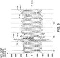
- Fig. 5 shows exemplary input voltage conditions in the motor drive in a normal operating mode and during a short transient condition without the selective bypass control of the present disclosure.
- the exemplary motor drive 110 operates in the second mode and the bus transient control 144c, 144c' selectively determines a selected phase among the phases to sequentially short while other phases are opened.
- Protective actions in the second mode provided by the bus transient control component reduces common mode voltage signals to less than 300 V.
- Figs. 6a and 6b show exemplary neutral resistor voltage conditions (e.g., across Rcm in Figs. 1 thru 3 above) in a normal operating mode and during a transient condition, where Fig. 6a shows operation without the selective bypass control of the present disclosure and Fig. 6b shows the situation where the selective bypassing in the second mode is used to inhibit common mode currents and voltages during a transient condition.
- Fig. 6a illustrates the voltage across a neutral resistor Rcm coupled between the input filter 112, 112' and the output filter 114, 114' of the drive when there is no protective bypass sequencing (e.g., without the exemplary mode controller 144m and the transient controller 144c, 144c' described above).
- Fig. 6a illustrates the voltage across a neutral resistor Rcm coupled between the input filter 112, 112' and the output filter 114, 114' of the drive when there is no protective bypass sequencing (e.g., without the exemplary mode controller 144m and the transient
- Fig. 6b illustrates a common mode voltage of less than 300 V when the bus transient control operates to signal sequencing of the phases such that no one or more phases are constantly being shorted during a transient condition, but rather all phases are sequentially shorted as a selected phase at any given time based on selection criteria.
- Fig. 7 is a flow diagram illustrating an exemplary method 200 for operating a power conversion system in accordance with further aspects of the disclosure. While the method 200 is illustrated and described below in the form of a series of acts or events, it will be appreciated that the various methods of the disclosure are not limited by the illustrated ordering of such acts or events, and that except as specifically provided hereinafter, some acts or events may occur in different order and/or concurrently with other acts or events apart from those illustrated and described herein. In addition, not all illustrated steps may be required to implement a process or method in accordance with the present disclosure, and one or more such acts may be combined.
- the illustrated methods may be implemented in hardware, processor-executed software, programmable logic, etc., or combinations thereof, in order to provide the motor drive control and protective circuit functionality described herein, and may be employed in any current source converter-based motor drive such as in the switching control system 140, 140' of the exemplary drives shown and described above, wherein the disclosure is not limited to the specifically illustrated and described applications and embodiments.
- the process 200 begins at 202 with the operation of the drive circuit inverter control component 144b providing inverter switching control signals 142b to the inverter 110b to convert the regulated DC current to provide AC electrical power to the AC output 114 according to at least one setpoint 141 in a normal mode of operation.
- the feedback system 118 monitors the drive 110 by sensing and/or otherwise determining the conditions of one or more components of the drive 110 including lines coupling inputs and outputs, for example, of the rectifier 110a, the intermediate DC circuit 150, the inverter 110b, etc.
- a determination is made at 206 as to whether the sensed motor condition(s) indicates a transient condition, for example, when a detected or sensed change in steady state conditions on the lines occur.
- the process proceeds to 212. If the motor conditions do not indicate a second (protective) mode situation (NO at 206), the controller 140 proceeds in a first (normal) operational mode with the rectifier controller 144a providing rectifier switching control signals 142a to the active rectifier 110a at 208 to convert AC electrical input power to provide a DC current Idc to the intermediate and to regulate (at 210) the current Idc according to a desired DC current value Idc* representing the requirements of the inverter 110b.
- the process 200 continues at 202 and 204 where the inverter control component 144b provides inverter switching control signals 142b to the inverter 110b to convert the regulated DC current to provide AC electrical power to the AC output 114 according to at least one setpoint 141, after which the process returns to 204 to continue monitoring the motor condition(s) for detecting transient conditions.
- a transient condition is determined (YES at 206)
- the process 200 proceeds in a second operational mode (protection mode) at 212 where bus control signals are provided to a rectifier control component 144a to sequentially bypass rectifier phases 121, 123, 125 of rectifier 110a to reduce a common mode current and/or voltage between input power and output power at terminals of the drive 110.
- a process flow or method 300 begins with inverter switching control signals being provided to convert DC current to output power to a motor load as discussed above in the current source motor drive circuit 110.
- the drive is monitored at 304 for transient conditions at 304, and a determination is made at 306 as to whether a transient condition is occurring.
- a protection mode is determined (YES at 306), the process flow continues at 312 and 314 as discussed below. Otherwise (NO at 306), the process 200 under a normal operation mode to provide rectifier switching control signals to the rectifier 110a to convert input power that is AC input current to DC current, with the DC current being regulated according to desired setpoints at 310 and the process repeats at 302 and 304 discussed above.
- the process continues to a second operational mode (circuit protection mode) at 312 with the bus transient control component 144c providing bus control signals in the switching control to sequentially bypass a selected rectifier phase 121, 123, or 125 according to selection criteria at any given time.
- At least one selection criteria is at least partially used to select the rectifier phase to short at 314.
- the selection criteria includes an absolute line-to-line voltage value (e.g., Vab, Vac, Vbc) in order to determine the phase at any given time that is shorted until the transient condition ceases. In certain embodiments, this involves selecting the phase that is not associated with a maximum absolute line-to-line input voltage.
- the process 200 then continues to monitor the drive for a transient condition or a change in steady state at 304.
- FIG. 9 Another embodiment is shown in Fig. 9 , in which a bypass phase is selected in the second mode which corresponds to the lowest absolute line-to-neutral voltage value.
- the process 400 begins at 402 (similar to 202 and 302 described above in connection with Figs. 7 and 8 ).
- the motor drive is monitored for transient conditions and a determination is made at 406 as to whether transients are occurring. If not (NO at 406), the drive operates in normal mode with rectifier switching signals provided to the rectifier 110a to convert inputted power to an outputted power according to a setpoint and at 410 the DC current is regulated. Otherwise (YES at 406), the process 400 proceeds to 412 to provide bus control signals to sequentially bypass selected rectifier phases according to selection criteria.
- selected rectifier phases are shorted based on selection criteria that includes an absolute line-to-neutral voltage. For example, a rectifier phase associated with the lowest absolute line-to-neutral input voltage during the protective mode of operation becomes the selected phase shorted at any given time.
- the rectifier phases are therefore shorted independently and separate from one another in a sequential pattern in order to reduce the common mode voltage of the drive. In other embodiments, more than one phase may be shorted while the phase or phases are opened.
- a non-transitory computer readable medium such as a computer memory, a memory within a power converter control system (e.g., switch control system 140 above), a CD-ROM, floppy disk, flash drive, database, server, computer, etc. which has computer executable instructions for performing the processes described above.
Landscapes
- Engineering & Computer Science (AREA)
- Power Engineering (AREA)
- Inverter Devices (AREA)
- Rectifiers (AREA)
Claims (7)
- Système de conversion de puissance comprenant :un redresseur actif (110a) comprenant une entrée en courant alternatif (112) comportant une pluralité de nœuds d'entrée en courant alternatif configurés pour recevoir une puissance d'entrée électrique alternative, une sortie en courant continu comportant des premier et second nœuds de sortie en courant continu, ainsi qu'un réseau de commutation de redresseur comprenant une pluralité de composants redresseurs de commutation (S1 à S6) qui forment une pluralité de phases redressées couplées individuellement entre l'un des nœuds d'entrée en courant alternatif et l'un des premier et second nœuds de sortie en courant continu, les composants redresseurs de commutation (S1 à S6) étant configurés individuellement pour coupler sélectivement le nœud d'entrée en courant alternatif au nœud de sortie correspondant en courant continu en fonction d'un signal correspondant de commande de commutation de redresseur (142a), etun onduleur (110b) comprenant une sortie en courant alternatif (114) comportant une pluralité de nœuds de sortie en courant alternatif configurés pour délivrer de l'énergie électrique alternative à une charge (120), ainsi qu'un réseau de commutation d'onduleur comprenant une pluralité de composants onduleurs de commutation (S7 à S12) couplés individuellement entre l'une d'une paire de lignes en courant continu et l'un des nœuds de sortie en courant alternatif, les composants onduleurs de commutation (S7 à S12) étant configurés individuellement pour coupler sélectivement électriquement la ligne de courant continu au nœud de sortie correspondant en courant alternatif en fonction d'un signal de commande de commutation d'onduleur (142b),un système de commande de commutation (140) configuré pour fonctionner sélectivement dans un premier mode de fonctionnement normal et dans un second mode de protection de circuits pendant des conditions transitoires de bus, le système de commande de commutation comprenant :un composant de commande d'onduleur (144b) configuré pour délivrer les signaux de commande de commutation d'onduleur (142b) dans les premier et second modes afin d'amener l'onduleur (110b) à convertir sélectivement du courant continu pour fournir de l'énergie électrique alternative à la sortie en courant alternatif conformément à au moins un point de réglage pour la charge,un composant de commande de redresseur (144a) configuré pour délivrer les signaux de commande de commutation de redresseur (142a) dans le premier mode afin de convertir l'énergie électrique d'entrée alternative pour fournir un courant continu régulé en fonction d'une valeur souhaitée de courant continu représentant les exigences de l'onduleur, etun composant de commande de transitoires de bus (144c) configuré pour fonctionner dans le second mode afin de délivrer au moins un signal ou une valeur de commande de transitoires de bus pour amener le composant de commande de redresseur à contourner sélectivement une phase sélectionnée du redresseur, les phases sélectionnées dans le redresseur étant contournées en court-circuitant des dispositifs de commutation dans la phase sélectionnée alors que des dispositifs de commutation d'autres phases sont ouverts, la phase sélectionnée l'étant sur la base d'au moins un critère de sélection pour réduire la tension ou le courant de mode commun entre l'entrée en courant alternatif et la sortie en courant alternatif tout en ouvrant des dispositifs de commutation associés aux autres phases,le système de conversion de puissance (100) comprenant en outre un circuit de rétroaction (118) procurant au moins un signal ou une valeur de rétroaction (118a) sur la base de l'état détecté du redresseur et de l'état détecté de l'onduleur, etun composant de commande de mode (144m) configuré pour placer le système de commande de commutation (140) soit dans le premier soit dans le second mode en fonction de la détermination de ce que le signal ou la valeur de rétroaction (118a) indique un état de transitoires,dans lequel le composant de commande de transitoires de bus (144c) est configuré pour contourner les phases de redresseur selon une suite séquentielle en court-circuitant la phase sélectionnée et en changeant la phase sélectionnée qui est court-circuitée en une autre phase sélectionnée jusqu'à ce qu'aucun état de transitoires ne soit détecté sur les nœuds d'entrée en courant alternatif du redresseur,caractérisé en ce que le ou les critères de sélection comprennent :la détermination de la phase sélectionnée à tout instant donné pendant le fonctionnement dans le second mode, en tant que phase associée à un nœud d'entrée en courant alternatif présentant une valeur absolue minimale de tension phase - neutre, qui est reçue en tant que signal ou valeur de rétroaction (118a), oula détermination de la phase sélectionnée à tout instant donné pendant le fonctionnement dans le second mode, en tant que phase non associée aux nœuds d'entrée en courant alternatif présentant la tension absolue phase - phase la plus élevée.
- Système selon la revendication 1, dans lequel le composant de commande de transitoires de bus est configuré pour contourner sélectivement la phase sélectionnée à différents instants en court-circuitant les composants redresseurs de commutation de la phase sélectionnée sur la base des critères de sélection.
- Système selon l'une des revendications 1 et 2, dans lequel le composant de commande de mode est configuré pour positionner le système de commande de commutation sur le second mode lorsqu'une distorsion détectée ou captée d'un état de régime permanent est présente au niveau de l'entrée en courant alternatif et/ou de la sortie en courant alternatif, et
dans lequel le composant de commande de transitoires est configuré pour détecter le second mode de fonctionnement et pour envoyer en réponse le ou les signaux de commande de transitoires de bus au composant de commande de redresseur. - Système selon l'une des revendications 1 à 3, comprenant une ligne de circuit couplée à l'entrée en courant alternatif, la sortie en courant alternatif pour un écoulement de courant se trouvant entre celles-ci, dans lequel le composant de commande de transitoires de bus réduit la tension de mode commun mesurée aux bornes de la ligne de circuit pendant le second mode de fonctionnement en régulant la valeur absolue de tension fonctionnelle aux bornes de la ligne de circuit à moins de 300 volts pour la protection du circuit, ou
le système de conversion de puissance est un circuit d'attaque de convertisseur de source de courant qui attaque une charge de moteur connectée à la sortie en courant alternatif pour recevoir l'énergie électrique alternative pendant le premier mode de fonctionnement et le second mode de fonctionnement, et il inclut un circuit en courant continu comprenant une inductance de liaison à courant continu dont les premier et second enroulements sont couplés dans des première et seconde lignes correspondantes en courant continu. - Procédé de mise en œuvre d'un système de conversion de puissance conforme à la revendication 1, le procédé comprenant :la délivrance (202) de signaux de commande de commutation d'onduleur à un onduleur afin de convertir un courant continu pour fournir de l'énergie électrique alternative à une sortie en courant alternatif couplée à une charge conformément à au moins un point de réglage,dans un premier mode fonctionnel du système de conversion de puissance, la délivrance (208) de signaux de commande de commutation de redresseur à un redresseur actif afin de convertir la puissance d'entrée électrique alternative au niveau d'une entrée en courant alternatif pour fournir un courant continu, l'entrée en courant alternatif comportant une pluralité de nœuds d'entrée en courant alternatif destinés à recevoir une puissance d'entrée électrique alternative,la surveillance (204) du système de conversion de puissance en ce qui concerne un état de transitoires, la surveillance (204) du système de conversion de puissance pour l'état de transitoires comprenant la détection des états du redresseur actif et de l'onduleur, etlors de la détermination (206) de ce que les états détectés indiquent un état de transitoires, le fonctionnement (212) dans un second mode fonctionnel du système de conversion de puissance qui comprend le contournement d'une phase de redresseur sélectionnée parmi une pluralité de phases sur lesquelles des dispositifs de commutation sont couplés à l'entrée en courant alternatif dans le but de réduire un courant en mode commun entre l'entrée en courant alternatif et la sortie en courant alternatif, les phases sélectionnées du redresseur étant contournées en court-circuitant les dispositifs de communication dans la phase sélectionnée alors que les dispositifs de communication d'autres phases restent ouverts,dans lequel la mise en œuvre (212) dans le second mode fonctionnel du système de conversion de puissance comprend en outre le contournement des phases de redresseur selon une suite séquentielle en court-circuitant la phase sélectionnée et en changeant la phase sélectionnée qui est court-circuitée en une autre phase sélectionnée jusqu'à ce qu'aucun état de transitoires ne soit détecté sur les nœuds d'entrée en courant alternatif du redresseur,caractérisé en ce que le ou les critères de sélection comprennent :la détermination de la phase sélectionnée à tout instant donné pendant le fonctionnement dans le second mode, en tant que phase associée à un nœud d'entrée en courant alternatif présentant une valeur absolue minimale de tension phase - neutre, qui est reçue en tant que signal ou valeur de rétroaction (118a), oula détermination de la phase sélectionnée à tout instant donné pendant le fonctionnement dans le second mode, en tant que phase non associée aux nœuds d'entrée en courant alternatif présentant la tension absolue phase - phase la plus élevée.
- Procédé selon la revendication 5, dans lequel le contournement d'une phase sélectionnée de redresseur comprend :le court-circuit d'une première phase de redresseur à un premier instant tout en ouvrant d'autres phases de redresseur,le court-circuit d'une deuxième phase de redresseur parmi les phases de redresseur à un deuxième instant tout en ouvrant d'autres phases de redresseur, etle court-circuit d'une troisième phase de redresseur à un troisième instant tout en ouvrant d'autres phases de redresseur.
- Support non transitoire pouvant être lu par ordinateur comprenant des instructions exécutables par ordinateur permettant de mettre en œuvre un système de conversion de puissance conforme à la revendication 1 de sorte à ce qu'il réalise les étapes du procédé conforme à la revendication 5.
Applications Claiming Priority (1)
| Application Number | Priority Date | Filing Date | Title |
|---|---|---|---|
| US13/029,209 US8570775B2 (en) | 2011-02-17 | 2011-02-17 | CMV reduction under bus transient condition |
Publications (3)
| Publication Number | Publication Date |
|---|---|
| EP2495863A2 EP2495863A2 (fr) | 2012-09-05 |
| EP2495863A3 EP2495863A3 (fr) | 2017-12-06 |
| EP2495863B1 true EP2495863B1 (fr) | 2021-12-15 |
Family
ID=45656058
Family Applications (1)
| Application Number | Title | Priority Date | Filing Date |
|---|---|---|---|
| EP12155964.5A Not-in-force EP2495863B1 (fr) | 2011-02-17 | 2012-02-17 | Réduction CMV sous des conditions transitoires de BUS |
Country Status (3)
| Country | Link |
|---|---|
| US (1) | US8570775B2 (fr) |
| EP (1) | EP2495863B1 (fr) |
| CN (1) | CN102647149B (fr) |
Families Citing this family (34)
| Publication number | Priority date | Publication date | Assignee | Title |
|---|---|---|---|---|
| US8379417B2 (en) | 2011-07-06 | 2013-02-19 | Rockwell Automation Technologies, Inc. | Power converter and integrated DC choke therefor |
| US8988026B2 (en) * | 2012-07-31 | 2015-03-24 | Rockwell Automation Technologies, Inc. | Single phase operation of a three-phase drive system |
| US9425705B2 (en) * | 2012-08-13 | 2016-08-23 | Rockwell Automation Technologies, Inc. | Method and apparatus for bypassing cascaded H-bridge (CHB) power cells and power sub cell for multilevel inverter |
| EP2773032A1 (fr) * | 2013-03-01 | 2014-09-03 | GE Energy Power Conversion Technology Ltd | Convertisseur alimenté par une source de courant imposé avec des composants blocable et une commutation spéciale |
| US9270198B2 (en) * | 2013-03-12 | 2016-02-23 | University Of Tennessee Research Foundation | Control of parallel-connected current source rectifiers |
| US9240731B2 (en) | 2013-03-18 | 2016-01-19 | Rockwell Automation Technologies, Inc. | Power cell bypass method and apparatus for multilevel inverter |
| CN104460794A (zh) * | 2013-09-25 | 2015-03-25 | 快捷半导体(苏州)有限公司 | 负载驱动方法、电路及其应用设备 |
| CN104682720A (zh) * | 2013-11-29 | 2015-06-03 | 东林科技股份有限公司 | 交交流电源转换装置及其转换方法 |
| EP2882083B1 (fr) * | 2013-12-05 | 2017-08-16 | ABB Schweiz AG | Circuit de correction du facteur de puissance sans pont |
| US9520800B2 (en) | 2014-01-09 | 2016-12-13 | Rockwell Automation Technologies, Inc. | Multilevel converter systems and methods with reduced common mode voltage |
| EP2911287A1 (fr) * | 2014-02-24 | 2015-08-26 | Danfoss Power Electronics A/S | Appareil et procédé de réduction d'harmoniques |
| US9559541B2 (en) | 2015-01-15 | 2017-01-31 | Rockwell Automation Technologies, Inc. | Modular multilevel converter and charging circuit therefor |
| US9748862B2 (en) | 2015-05-13 | 2017-08-29 | Rockwell Automation Technologies, Inc. | Sparse matrix multilevel actively clamped power converter |
| CN106921299A (zh) * | 2015-12-25 | 2017-07-04 | 通用电气公司 | 功率变换系统 |
| AT518371A1 (de) * | 2016-01-25 | 2017-09-15 | Eco-S Green Solutions Kg | Schaltungsanordnung für einen Frequenzumrichter |
| US10263558B2 (en) * | 2016-03-16 | 2019-04-16 | Rockwell Automation Technologies, Inc. | Phase loss detection in active front end converters |
| US9960723B2 (en) * | 2016-06-06 | 2018-05-01 | Rockwell Automation Technologies, Inc. | Motor drive with resonance detection and impedance computation |
| GB201610369D0 (en) * | 2016-06-15 | 2016-07-27 | Rolls Royce Plc | Control of an electrical converter |
| US9812990B1 (en) | 2016-09-26 | 2017-11-07 | Rockwell Automation Technologies, Inc. | Spare on demand power cells for modular multilevel power converter |
| CN110168852B (zh) * | 2016-11-09 | 2023-12-12 | Abb瑞士股份有限公司 | 具有旁路的三线多相ups |
| US9973102B1 (en) * | 2016-12-23 | 2018-05-15 | Rockwell Automation Technologies, Inc. | System for power conversion with feedback to reduce DC bus loading |
| JP6797748B2 (ja) * | 2017-03-21 | 2020-12-09 | 株式会社東芝 | 電力変換装置及び電力変換システム |
| CN107070361B (zh) * | 2017-03-30 | 2019-02-12 | 沈阳工业大学 | 一种降低六相电动机共模电压的svpwm控制方法 |
| JP6781343B2 (ja) * | 2017-06-21 | 2020-11-04 | 東芝三菱電機産業システム株式会社 | サイリスタ起動装置 |
| US10158299B1 (en) * | 2018-04-18 | 2018-12-18 | Rockwell Automation Technologies, Inc. | Common voltage reduction for active front end drives |
| US11251741B2 (en) * | 2018-11-15 | 2022-02-15 | Eaton Intelligent Power Limited | Modular board-level motor control system with integrated protection and control components |
| US10784797B1 (en) * | 2019-06-19 | 2020-09-22 | Rockwell Automation Technologies, Inc. | Bootstrap charging by PWM control |
| CN110401355B (zh) * | 2019-07-31 | 2020-12-22 | 河北工业大学 | 一种抑制共模电压的间接矩阵变换器调制方法 |
| US11211879B2 (en) | 2019-09-23 | 2021-12-28 | Rockwell Automation Technologies, Inc. | Capacitor size reduction and lifetime extension for cascaded H-bridge drives |
| KR102942078B1 (ko) | 2019-12-18 | 2026-03-23 | 삼성전자주식회사 | 전자 장치 및 전원 공급 장치 |
| EP3972121B1 (fr) * | 2020-09-18 | 2023-11-01 | Schneider Toshiba Inverter Europe SAS | Procédés et dispositifs pour atténuer des courants en mode commun dans des systèmes d'alimentation ca |
| CN114460994B (zh) * | 2020-11-09 | 2024-09-27 | 扬智科技股份有限公司 | 电压调整器 |
| US11342878B1 (en) | 2021-04-09 | 2022-05-24 | Rockwell Automation Technologies, Inc. | Regenerative medium voltage drive (Cascaded H Bridge) with reduced number of sensors |
| CN114337205B (zh) * | 2022-03-09 | 2022-06-03 | 河北工业大学 | 一种机器人伺服驱动器imc的共模峰值抑制方法 |
Family Cites Families (15)
| Publication number | Priority date | Publication date | Assignee | Title |
|---|---|---|---|---|
| US5905642A (en) | 1997-11-11 | 1999-05-18 | Robicon Corporation | Apparatus and method to reduce common mode voltage from current source drives |
| USRE38439E1 (en) * | 1999-05-12 | 2004-02-24 | Otis Elevator Company | Control of a DC matrix converter |
| JP2005033895A (ja) * | 2003-07-10 | 2005-02-03 | Toshiba Corp | 電力変換装置 |
| US7782009B2 (en) | 2004-08-24 | 2010-08-24 | Rockwell Automation Technologies, Inc. | Adjustable speed drive protection |
| US7301789B2 (en) | 2004-08-24 | 2007-11-27 | Rockwell Automation Technologies, Inc. | Adjustable speed drive protection |
| US7808763B2 (en) | 2004-08-24 | 2010-10-05 | Rockwell Automation Technologies, Inc. | Adjustable speed drive protection |
| US7215559B2 (en) * | 2004-09-28 | 2007-05-08 | Rockwell Automation Technologies, Inc. | Method and apparatus to reduce common mode voltages applied to a load by a drive |
| JP4760000B2 (ja) * | 2004-12-09 | 2011-08-31 | ダイキン工業株式会社 | 多相電流供給回路、駆動装置、圧縮機、及び空気調和機 |
| JP4645808B2 (ja) * | 2004-12-17 | 2011-03-09 | サンケン電気株式会社 | 3相電力変換装置 |
| US7368890B2 (en) * | 2006-02-07 | 2008-05-06 | Rockwell Automation Technologies, Inc. | Power converter with active discharging for improved auto-restart capability |
| US7274576B1 (en) * | 2006-03-01 | 2007-09-25 | Rockwell Automation Technologies, Inc. | Power converter with reduced common mode voltage |
| JP4862477B2 (ja) * | 2006-05-10 | 2012-01-25 | 株式会社明電舎 | 交流−交流直接変換装置の入出力デューティ制御方法 |
| US7602132B2 (en) * | 2006-09-27 | 2009-10-13 | Rockwell Automation Technologies, Inc. | Methods and system for motor drive information capture |
| US7990097B2 (en) * | 2008-09-29 | 2011-08-02 | Rockwell Automation Technologies, Inc. | Power conversion system and method for active damping of common mode resonance |
| US8223511B2 (en) * | 2010-06-07 | 2012-07-17 | Rockwell Automation Technologies, Inc. | Common mode voltage reduction apparatus and method for current source converter based drive |
-
2011
- 2011-02-17 US US13/029,209 patent/US8570775B2/en active Active
-
2012
- 2012-02-17 EP EP12155964.5A patent/EP2495863B1/fr not_active Not-in-force
- 2012-02-17 CN CN201210037296.5A patent/CN102647149B/zh not_active Expired - Fee Related
Also Published As
| Publication number | Publication date |
|---|---|
| CN102647149B (zh) | 2014-12-03 |
| CN102647149A (zh) | 2012-08-22 |
| US8570775B2 (en) | 2013-10-29 |
| EP2495863A2 (fr) | 2012-09-05 |
| EP2495863A3 (fr) | 2017-12-06 |
| US20120212982A1 (en) | 2012-08-23 |
Similar Documents
| Publication | Publication Date | Title |
|---|---|---|
| EP2495863B1 (fr) | Réduction CMV sous des conditions transitoires de BUS | |
| EP2393197B1 (fr) | Appareil de réduction de tension en mode commun et procédé pour entraînement basé sur un convertisseur de source de courant | |
| US8937796B2 (en) | Variable frequency drive and methods for filter capacitor fault detection | |
| EP2320548B1 (fr) | Procédé de survoltage de bus CC et système pour frein par récupération | |
| US8476859B2 (en) | DC power for SGCT devices using a high frequency current loop with multiple current transformers | |
| JP6207730B2 (ja) | 直流送電電力変換装置および直流送電電力変換方法 | |
| US9362839B2 (en) | Power converter with common mode voltage reduction | |
| US20110057588A1 (en) | Dynamic braking for current source converter based drive | |
| JP2010187431A (ja) | 無停電電源装置 | |
| JP5145124B2 (ja) | 電力変換装置 | |
| CN107370389B (zh) | 用于克服异常电网状况的电力转换系统及其操作方法 | |
| CN100399697C (zh) | 绕线式转子感应电动机的控制器 | |
| JP6091405B2 (ja) | エレベーターかご給電装置 | |
| CN118202540A (zh) | 在电网中稳定电功率 | |
| JP4487155B2 (ja) | Pwmサイクロコンバータの保護装置 | |
| CN105471358A (zh) | 电动机控制装置 | |
| JP4235910B2 (ja) | 巻線形誘導電動機の制御装置 | |
| JP7417836B2 (ja) | インバータ制御装置および方法 | |
| JPH02219499A (ja) | 交流電動機の駆動制御装置 | |
| JP2009254122A (ja) | 電力変換装置の制御回路 | |
| Capecce et al. | A new control technique for harmonics elimination in six-switch active rectifiers | |
| Mukherjee et al. | A Series Connected Three-Level Inverter Topology For Medium Voltage Squirrel Cage Motor Drive Applications | |
| Yıldırım | Field Oriented Control of a Permanent Magnet Synchronous Motor Using Space Vector Modulated Direct AC-AC Matrix Converter |
Legal Events
| Date | Code | Title | Description |
|---|---|---|---|
| PUAI | Public reference made under article 153(3) epc to a published international application that has entered the european phase |
Free format text: ORIGINAL CODE: 0009012 |
|
| AK | Designated contracting states |
Kind code of ref document: A2 Designated state(s): AL AT BE BG CH CY CZ DE DK EE ES FI FR GB GR HR HU IE IS IT LI LT LU LV MC MK MT NL NO PL PT RO RS SE SI SK SM TR |
|
| AX | Request for extension of the european patent |
Extension state: BA ME |
|
| PUAL | Search report despatched |
Free format text: ORIGINAL CODE: 0009013 |
|
| AK | Designated contracting states |
Kind code of ref document: A3 Designated state(s): AL AT BE BG CH CY CZ DE DK EE ES FI FR GB GR HR HU IE IS IT LI LT LU LV MC MK MT NL NO PL PT RO RS SE SI SK SM TR |
|
| AX | Request for extension of the european patent |
Extension state: BA ME |
|
| RIC1 | Information provided on ipc code assigned before grant |
Ipc: H02M 1/32 20070101ALI20171102BHEP Ipc: H02M 5/458 20060101AFI20171102BHEP Ipc: H02M 7/219 20060101ALI20171102BHEP Ipc: H02M 7/12 20060101ALI20171102BHEP |
|
| STAA | Information on the status of an ep patent application or granted ep patent |
Free format text: STATUS: REQUEST FOR EXAMINATION WAS MADE |
|
| 17P | Request for examination filed |
Effective date: 20180606 |
|
| RBV | Designated contracting states (corrected) |
Designated state(s): AL AT BE BG CH CY CZ DE DK EE ES FI FR GB GR HR HU IE IS IT LI LT LU LV MC MK MT NL NO PL PT RO RS SE SI SK SM TR |
|
| STAA | Information on the status of an ep patent application or granted ep patent |
Free format text: STATUS: EXAMINATION IS IN PROGRESS |
|
| 17Q | First examination report despatched |
Effective date: 20181119 |
|
| GRAP | Despatch of communication of intention to grant a patent |
Free format text: ORIGINAL CODE: EPIDOSNIGR1 |
|
| STAA | Information on the status of an ep patent application or granted ep patent |
Free format text: STATUS: GRANT OF PATENT IS INTENDED |
|
| RIC1 | Information provided on ipc code assigned before grant |
Ipc: H02M 5/458 20060101AFI20210527BHEP Ipc: H02M 7/219 20060101ALI20210527BHEP Ipc: H02M 1/32 20070101ALI20210527BHEP Ipc: H02M 7/12 20060101ALI20210527BHEP Ipc: H02P 27/06 20060101ALI20210527BHEP Ipc: H02P 29/024 20160101ALI20210527BHEP |
|
| INTG | Intention to grant announced |
Effective date: 20210625 |
|
| GRAS | Grant fee paid |
Free format text: ORIGINAL CODE: EPIDOSNIGR3 |
|
| GRAA | (expected) grant |
Free format text: ORIGINAL CODE: 0009210 |
|
| STAA | Information on the status of an ep patent application or granted ep patent |
Free format text: STATUS: THE PATENT HAS BEEN GRANTED |
|
| AK | Designated contracting states |
Kind code of ref document: B1 Designated state(s): AL AT BE BG CH CY CZ DE DK EE ES FI FR GB GR HR HU IE IS IT LI LT LU LV MC MK MT NL NO PL PT RO RS SE SI SK SM TR |
|
| REG | Reference to a national code |
Ref country code: GB Ref legal event code: FG4D Ref country code: CH Ref legal event code: EP |
|
| REG | Reference to a national code |
Ref country code: DE Ref legal event code: R096 Ref document number: 602012077349 Country of ref document: DE |
|
| REG | Reference to a national code |
Ref country code: IE Ref legal event code: FG4D |
|
| REG | Reference to a national code |
Ref country code: AT Ref legal event code: REF Ref document number: 1456225 Country of ref document: AT Kind code of ref document: T Effective date: 20220115 |
|
| REG | Reference to a national code |
Ref country code: LT Ref legal event code: MG9D |
|
| REG | Reference to a national code |
Ref country code: NL Ref legal event code: MP Effective date: 20211215 |
|
| PG25 | Lapsed in a contracting state [announced via postgrant information from national office to epo] |
Ref country code: RS Free format text: LAPSE BECAUSE OF FAILURE TO SUBMIT A TRANSLATION OF THE DESCRIPTION OR TO PAY THE FEE WITHIN THE PRESCRIBED TIME-LIMIT Effective date: 20211215 Ref country code: LT Free format text: LAPSE BECAUSE OF FAILURE TO SUBMIT A TRANSLATION OF THE DESCRIPTION OR TO PAY THE FEE WITHIN THE PRESCRIBED TIME-LIMIT Effective date: 20211215 Ref country code: FI Free format text: LAPSE BECAUSE OF FAILURE TO SUBMIT A TRANSLATION OF THE DESCRIPTION OR TO PAY THE FEE WITHIN THE PRESCRIBED TIME-LIMIT Effective date: 20211215 Ref country code: BG Free format text: LAPSE BECAUSE OF FAILURE TO SUBMIT A TRANSLATION OF THE DESCRIPTION OR TO PAY THE FEE WITHIN THE PRESCRIBED TIME-LIMIT Effective date: 20220315 |
|
| REG | Reference to a national code |
Ref country code: AT Ref legal event code: MK05 Ref document number: 1456225 Country of ref document: AT Kind code of ref document: T Effective date: 20211215 |
|
| PG25 | Lapsed in a contracting state [announced via postgrant information from national office to epo] |
Ref country code: SE Free format text: LAPSE BECAUSE OF FAILURE TO SUBMIT A TRANSLATION OF THE DESCRIPTION OR TO PAY THE FEE WITHIN THE PRESCRIBED TIME-LIMIT Effective date: 20211215 Ref country code: NO Free format text: LAPSE BECAUSE OF FAILURE TO SUBMIT A TRANSLATION OF THE DESCRIPTION OR TO PAY THE FEE WITHIN THE PRESCRIBED TIME-LIMIT Effective date: 20220315 Ref country code: LV Free format text: LAPSE BECAUSE OF FAILURE TO SUBMIT A TRANSLATION OF THE DESCRIPTION OR TO PAY THE FEE WITHIN THE PRESCRIBED TIME-LIMIT Effective date: 20211215 Ref country code: HR Free format text: LAPSE BECAUSE OF FAILURE TO SUBMIT A TRANSLATION OF THE DESCRIPTION OR TO PAY THE FEE WITHIN THE PRESCRIBED TIME-LIMIT Effective date: 20211215 Ref country code: GR Free format text: LAPSE BECAUSE OF FAILURE TO SUBMIT A TRANSLATION OF THE DESCRIPTION OR TO PAY THE FEE WITHIN THE PRESCRIBED TIME-LIMIT Effective date: 20220316 |
|
| PG25 | Lapsed in a contracting state [announced via postgrant information from national office to epo] |
Ref country code: NL Free format text: LAPSE BECAUSE OF FAILURE TO SUBMIT A TRANSLATION OF THE DESCRIPTION OR TO PAY THE FEE WITHIN THE PRESCRIBED TIME-LIMIT Effective date: 20211215 |
|
| PG25 | Lapsed in a contracting state [announced via postgrant information from national office to epo] |
Ref country code: SM Free format text: LAPSE BECAUSE OF FAILURE TO SUBMIT A TRANSLATION OF THE DESCRIPTION OR TO PAY THE FEE WITHIN THE PRESCRIBED TIME-LIMIT Effective date: 20211215 Ref country code: SK Free format text: LAPSE BECAUSE OF FAILURE TO SUBMIT A TRANSLATION OF THE DESCRIPTION OR TO PAY THE FEE WITHIN THE PRESCRIBED TIME-LIMIT Effective date: 20211215 Ref country code: RO Free format text: LAPSE BECAUSE OF FAILURE TO SUBMIT A TRANSLATION OF THE DESCRIPTION OR TO PAY THE FEE WITHIN THE PRESCRIBED TIME-LIMIT Effective date: 20211215 Ref country code: PT Free format text: LAPSE BECAUSE OF FAILURE TO SUBMIT A TRANSLATION OF THE DESCRIPTION OR TO PAY THE FEE WITHIN THE PRESCRIBED TIME-LIMIT Effective date: 20220418 Ref country code: ES Free format text: LAPSE BECAUSE OF FAILURE TO SUBMIT A TRANSLATION OF THE DESCRIPTION OR TO PAY THE FEE WITHIN THE PRESCRIBED TIME-LIMIT Effective date: 20211215 Ref country code: EE Free format text: LAPSE BECAUSE OF FAILURE TO SUBMIT A TRANSLATION OF THE DESCRIPTION OR TO PAY THE FEE WITHIN THE PRESCRIBED TIME-LIMIT Effective date: 20211215 Ref country code: CZ Free format text: LAPSE BECAUSE OF FAILURE TO SUBMIT A TRANSLATION OF THE DESCRIPTION OR TO PAY THE FEE WITHIN THE PRESCRIBED TIME-LIMIT Effective date: 20211215 |
|
| PG25 | Lapsed in a contracting state [announced via postgrant information from national office to epo] |
Ref country code: PL Free format text: LAPSE BECAUSE OF FAILURE TO SUBMIT A TRANSLATION OF THE DESCRIPTION OR TO PAY THE FEE WITHIN THE PRESCRIBED TIME-LIMIT Effective date: 20211215 Ref country code: AT Free format text: LAPSE BECAUSE OF FAILURE TO SUBMIT A TRANSLATION OF THE DESCRIPTION OR TO PAY THE FEE WITHIN THE PRESCRIBED TIME-LIMIT Effective date: 20211215 |
|
| REG | Reference to a national code |
Ref country code: DE Ref legal event code: R097 Ref document number: 602012077349 Country of ref document: DE |
|
| PG25 | Lapsed in a contracting state [announced via postgrant information from national office to epo] |
Ref country code: MC Free format text: LAPSE BECAUSE OF FAILURE TO SUBMIT A TRANSLATION OF THE DESCRIPTION OR TO PAY THE FEE WITHIN THE PRESCRIBED TIME-LIMIT Effective date: 20211215 Ref country code: IS Free format text: LAPSE BECAUSE OF FAILURE TO SUBMIT A TRANSLATION OF THE DESCRIPTION OR TO PAY THE FEE WITHIN THE PRESCRIBED TIME-LIMIT Effective date: 20220415 |
|
| REG | Reference to a national code |
Ref country code: CH Ref legal event code: PL |
|
| PLBE | No opposition filed within time limit |
Free format text: ORIGINAL CODE: 0009261 |
|
| STAA | Information on the status of an ep patent application or granted ep patent |
Free format text: STATUS: NO OPPOSITION FILED WITHIN TIME LIMIT |
|
| REG | Reference to a national code |
Ref country code: BE Ref legal event code: MM Effective date: 20220228 |
|
| PG25 | Lapsed in a contracting state [announced via postgrant information from national office to epo] |
Ref country code: LU Free format text: LAPSE BECAUSE OF NON-PAYMENT OF DUE FEES Effective date: 20220217 Ref country code: DK Free format text: LAPSE BECAUSE OF FAILURE TO SUBMIT A TRANSLATION OF THE DESCRIPTION OR TO PAY THE FEE WITHIN THE PRESCRIBED TIME-LIMIT Effective date: 20211215 Ref country code: AL Free format text: LAPSE BECAUSE OF FAILURE TO SUBMIT A TRANSLATION OF THE DESCRIPTION OR TO PAY THE FEE WITHIN THE PRESCRIBED TIME-LIMIT Effective date: 20211215 |
|
| 26N | No opposition filed |
Effective date: 20220916 |
|
| PG25 | Lapsed in a contracting state [announced via postgrant information from national office to epo] |
Ref country code: SI Free format text: LAPSE BECAUSE OF FAILURE TO SUBMIT A TRANSLATION OF THE DESCRIPTION OR TO PAY THE FEE WITHIN THE PRESCRIBED TIME-LIMIT Effective date: 20211215 |
|
| PG25 | Lapsed in a contracting state [announced via postgrant information from national office to epo] |
Ref country code: LI Free format text: LAPSE BECAUSE OF NON-PAYMENT OF DUE FEES Effective date: 20220228 Ref country code: IE Free format text: LAPSE BECAUSE OF NON-PAYMENT OF DUE FEES Effective date: 20220217 Ref country code: CH Free format text: LAPSE BECAUSE OF NON-PAYMENT OF DUE FEES Effective date: 20220228 |
|
| PG25 | Lapsed in a contracting state [announced via postgrant information from national office to epo] |
Ref country code: BE Free format text: LAPSE BECAUSE OF NON-PAYMENT OF DUE FEES Effective date: 20220228 |
|
| PG25 | Lapsed in a contracting state [announced via postgrant information from national office to epo] |
Ref country code: IT Free format text: LAPSE BECAUSE OF FAILURE TO SUBMIT A TRANSLATION OF THE DESCRIPTION OR TO PAY THE FEE WITHIN THE PRESCRIBED TIME-LIMIT Effective date: 20211215 |
|
| P01 | Opt-out of the competence of the unified patent court (upc) registered |
Effective date: 20230404 |
|
| PG25 | Lapsed in a contracting state [announced via postgrant information from national office to epo] |
Ref country code: HU Free format text: LAPSE BECAUSE OF FAILURE TO SUBMIT A TRANSLATION OF THE DESCRIPTION OR TO PAY THE FEE WITHIN THE PRESCRIBED TIME-LIMIT; INVALID AB INITIO Effective date: 20120217 |
|
| PG25 | Lapsed in a contracting state [announced via postgrant information from national office to epo] |
Ref country code: MK Free format text: LAPSE BECAUSE OF FAILURE TO SUBMIT A TRANSLATION OF THE DESCRIPTION OR TO PAY THE FEE WITHIN THE PRESCRIBED TIME-LIMIT Effective date: 20211215 Ref country code: CY Free format text: LAPSE BECAUSE OF FAILURE TO SUBMIT A TRANSLATION OF THE DESCRIPTION OR TO PAY THE FEE WITHIN THE PRESCRIBED TIME-LIMIT Effective date: 20211215 |
|
| PGFP | Annual fee paid to national office [announced via postgrant information from national office to epo] |
Ref country code: DE Payment date: 20240123 Year of fee payment: 13 Ref country code: GB Payment date: 20240123 Year of fee payment: 13 |
|
| PGFP | Annual fee paid to national office [announced via postgrant information from national office to epo] |
Ref country code: FR Payment date: 20240123 Year of fee payment: 13 |
|
| PG25 | Lapsed in a contracting state [announced via postgrant information from national office to epo] |
Ref country code: MT Free format text: LAPSE BECAUSE OF FAILURE TO SUBMIT A TRANSLATION OF THE DESCRIPTION OR TO PAY THE FEE WITHIN THE PRESCRIBED TIME-LIMIT Effective date: 20211215 |
|
| REG | Reference to a national code |
Ref country code: DE Ref legal event code: R119 Ref document number: 602012077349 Country of ref document: DE |
|
| GBPC | Gb: european patent ceased through non-payment of renewal fee |
Effective date: 20250217 |
|
| PG25 | Lapsed in a contracting state [announced via postgrant information from national office to epo] |
Ref country code: TR Free format text: LAPSE BECAUSE OF FAILURE TO SUBMIT A TRANSLATION OF THE DESCRIPTION OR TO PAY THE FEE WITHIN THE PRESCRIBED TIME-LIMIT Effective date: 20211215 |
|
| PG25 | Lapsed in a contracting state [announced via postgrant information from national office to epo] |
Ref country code: DE Free format text: LAPSE BECAUSE OF NON-PAYMENT OF DUE FEES Effective date: 20250902 |
|
| PG25 | Lapsed in a contracting state [announced via postgrant information from national office to epo] |
Ref country code: GB Free format text: LAPSE BECAUSE OF NON-PAYMENT OF DUE FEES Effective date: 20250217 |
|
| PG25 | Lapsed in a contracting state [announced via postgrant information from national office to epo] |
Ref country code: FR Free format text: LAPSE BECAUSE OF NON-PAYMENT OF DUE FEES Effective date: 20250228 |