EP2511952A1 - Stacked composite device including a group III-V transistor and a group IV vertical transistor - Google Patents
Stacked composite device including a group III-V transistor and a group IV vertical transistor Download PDFInfo
- Publication number
- EP2511952A1 EP2511952A1 EP12163106A EP12163106A EP2511952A1 EP 2511952 A1 EP2511952 A1 EP 2511952A1 EP 12163106 A EP12163106 A EP 12163106A EP 12163106 A EP12163106 A EP 12163106A EP 2511952 A1 EP2511952 A1 EP 2511952A1
- Authority
- EP
- European Patent Office
- Prior art keywords
- transistor
- group
- composite
- composite device
- iii
- Prior art date
- Legal status (The legal status is an assumption and is not a legal conclusion. Google has not performed a legal analysis and makes no representation as to the accuracy of the status listed.)
- Granted
Links
Images



Classifications
-
- H—ELECTRICITY
- H10—SEMICONDUCTOR DEVICES; ELECTRIC SOLID-STATE DEVICES NOT OTHERWISE PROVIDED FOR
- H10W—GENERIC PACKAGES, INTERCONNECTIONS, CONNECTORS OR OTHER CONSTRUCTIONAL DETAILS OF DEVICES COVERED BY CLASS H10
- H10W90/00—Package configurations
-
- H—ELECTRICITY
- H03—ELECTRONIC CIRCUITRY
- H03K—PULSE TECHNIQUE
- H03K17/00—Electronic switching or gating, i.e. not by contact-making and –breaking
- H03K17/51—Electronic switching or gating, i.e. not by contact-making and –breaking characterised by the components used
- H03K17/56—Electronic switching or gating, i.e. not by contact-making and –breaking characterised by the components used by the use, as active elements, of semiconductor devices
- H03K17/567—Circuits characterised by the use of more than one type of semiconductor device, e.g. BIMOS, composite devices such as IGBT
Definitions
- group III-V refers to a compound semiconductor including at least one group III element and at least one group V element.
- a group III-V semiconductor may take the form of a III-Nitride semiconductor.
- III-Nitride or “III-N” refers to a compound semiconductor that includes nitrogen and at least one group III element including aluminum (Al), gallium (Ga), indium (In), and boron (B), and including but not limited to any of its alloys, such as aluminum gallium nitride (Al x Ga (1-x) N), indium gallium nitride (In y Ga (1-y) N), aluminum indium gallium nitride (Al x In y Ga (1-x-y) N), gallium arsenide phosphide nitride (GaAs a P b N (1-a-b )), aluminum indium gallium arsenide phosphide nitride (Al
- III-Nitride also refers generally to any polarity including but not limited to Ga-polar, N-polar, semi-polar or non-polar crystal orientations.
- a III-Nitride material may also include either the Wurtzitic, Zincblende or mixed polytypes, and may include single-crystal, monocrystalline, polycrystalline, or amorphous structures.
- group IV refers to a semiconductor that includes at least one group four element including silicon (Si), germanium (Ge) and carbon (C), and also includes compound semiconductors such as silicon germanium (SiGe) and silicon carbide (SiC), for example.
- Group IV also refers to semiconductor materials which include more than one layer of group IV elements, or doping of group IV elements to produce strained group IV material, and may also include group IV based composite substrates such as silicon on insulstor (SOI), separation by implantation of oxygen (SIMOX) process substrates, and silicon on sapphire (SOS), for example.
- SOI silicon on insulstor
- SIMOX separation by implantation of oxygen
- SOS silicon on sapphire
- LV device refers to a low-voltage device. Typical voltage ratings include LV ⁇ 0V-50V, midvoltage (MV) ⁇ 50V-300V, and high-voltage (HV) ⁇ 300V-1200V.
- III-Nitride transistors such as gallium nitride (GaN) field-effect transistors (FETs) and high mobility electron transistors (HEMTs) are often desirable for their high efficiency and high-voltage operation. Moreover, it is often desirable to combine such III-Nitride transistors with other FETs, such as silicon FETs, to create high performance composite switching devices.
- GaN gallium nitride
- FETs field-effect transistors
- HEMTs high mobility electron transistors
- a depletion mode (normally ON) III-Nitride transistor can be cascoded with an enhancement mode (normally OFF) low-voltage (LV) or midvoltage (MV) group IV semiconductor transistor, for example a silicon FET, to produce an enhancement mode (normally OFF) composite power device.
- an enhancement mode normally OFF
- LV low-voltage
- MV midvoltage
- conventional packaging techniques for combining III-Nitride transistors with silicon FETs for example, often counterweigh the benefits provided by III-Nitride devices.
- conventional package designs may place discrete components side-by-side on a common support surface implemented using a ceramic based substrate such as a direct bonded copper (DBC) substrate, or a ceramic substrate on a lead-frame.
- DBC direct bonded copper
- Such side-by-side configuration can undesirably increase the parasitic inductance and resistance in the current paths of the composite power device, and would also increase the thermal dissipation requirements of the package.
- the side-by-side placement of devices on a common substrate can undesirably increase package form factor, as well as manufacturing costs.
- the present disclosure is directed to a stacked composite device including a group III-V transistor and a group IV vertical transistor, substantially as shown in and/or described in connection with at least one of the figures, and as set forth more completely in the claims.
- III-Nitride materials include, for example, gallium nitride (GaN) and its alloys such as aluminum gallium nitride (AlGaN), indium gallium nitride (InGaN), and aluminum indium gallium nitride (AlInGaN). These materials are semiconductor compounds that have a relatively wide, direct bandgap and strong piezoelectric polarizations, and can enable high breakdown fields, high saturation velocities, and the creation of two-dimensional electron gases (2DEGs).
- GaN gallium nitride
- AlGaN aluminum gallium nitride
- InGaN indium gallium nitride
- AlInGaN aluminum indium gallium nitride
- III-Nitride materials such as GaN are used in many microelectronic applications as depletion mode (e.g., normally ON) and enhancement mode (e.g., normally OFF) power field-effect transistors (FETs) and high electron mobility transistors (HEMTs), for example.
- depletion mode e.g., normally ON
- enhancement mode e.g., normally OFF
- FETs field-effect transistors
- HEMTs high electron mobility transistors
- a depletion mode III-Nitride or other group III-V device can be cascoded with a low-voltage (LV) or midvoltage (MV) group IV semiconductor device to produce an enhancement mode composite power device.
- LV low-voltage
- MV midvoltage
- the utility and reliability of such a composite device can be compromised by conventional packaging techniques for combining III-Nitride transistors with silicon or other group IV semiconductor FETs, which can often negate the benefits provided by III-Nitride devices.
- conventional package designs may place discrete components side-by-side on a common support surface implemented using a ceramic based substrate such as a direct bonded copper (DBC) substrate, or a ceramic substrate on a lead-frame.
- DBC direct bonded copper
- Such side-by-side configuration can undesirably increase the parasitic inductance and resistance in the current paths of the composite power device, and would also increase the thermal dissipation requirements of the package.
- the side-by-side placement of devices on a common substrate can undesirably increase package form factor, as well as manufacturing costs.
- a compact and cost-effective packaging solution for integrating III-Nitride or other group III-V transistors with group IV FETs, such as silicon FETs is needed.
- the present application is directed to a stacked composite device wherein the group III-V active die is stacked on top of a silicon or group IV active die having a vertical transistor formed therein.
- the present approach is motivated in part by the larger die size typically required for the bottom die. That is to say, by implementing the bottom (larger) active die of the composite device using a less expensive group IV material such as silicon, and stacking a smaller active die formed of a costlier group III-V material such as GaN over the smaller group IV active die, the present application discloses a compact, cost effective packaging solution advantageously providing the performance advantages enabled by group III-V transistors.
- the stacked composite device may include a III-Nitride power transistor cascoded with an LV or MV group IV vertical transistor.
- the cascoded combination of the III-Nitride power transistor which may be a normally ON device, for example, with the LV or MV group IV vertical transistor can be implemented to produce a normally OFF composite power device.
- the composite device configurations disclosed by the present application are designed to substantially reduce parasitic inductance and resistance, and enhance thermal dissipation by a composite device package when compared to conventional integrated packaging solutions.
- Figure 1 shows one exemplary implementation of a composite device.
- composite device 101 includes group III-V transistor 110 cascoded with group IV transistor 120.
- composite source 102, composite drain 104, and composite gate 106 of composite device 101 are also shown in Figure 1 .
- Group III-V transistor 110 may be a III-Nitride power transistor and may be implemented as an insulated-gate FET (IGFET), or as a heterostructure FET (HFET), for example.
- group III-V transistor 110 may take the form of a metal-insulator-semiconductor FET (MISFET), such as a metal-oxide-semiconductor FET (MOSFET).
- MISFET metal-insulator-semiconductor FET
- group III-V transistor 110 when implemented as an HFET, group III-V transistor 110 may be a HEMT configured to produce a 2DEG.
- group III-V transistor 110 may be a high-voltage (HV) device configured to sustain a drain voltage of approximately 600V and having a gate rating of approximately 40V.
- HV high-voltage
- composite device 101 1 may utilize an insulated gate bipolar transistor (IGBT) as a power transistor in place of a group III-V FET or HEMT. It is further noted that composite device 101 may utilize a group III-V FET or HEMT other than a III-N FET or HEMT, such as a III-As, III-P or III-As a P b N (1-a-b) FET or HEMT, for example, as group III-V transistor 110.
- IGBT insulated gate bipolar transistor
- Group IV transistor 120 may be implemented as an LV or MV group IV vertical transistor, such as a silicon vertical transistor having a breakdown voltage in a range from approximately 25V to approximately 250V, for example.
- group IV transistor 120 may be a silicon vertical MISFET or MOSFET, for example.
- group IV transistor 120 may include any suitable group IV material, such as silicon carbide (SiC), germanium (Ge), silicon germanium (SiGe), or a strained group IV element or compound, for example.
- composite device 101 which according to the implementation shown in Figure 1 results in a composite three terminal device functioning in effect as a composite transistor having composite source 102 and composite gate 106 provided by group IV transistor 120, and composite drain 104 provided by group III-V transistor 110.
- composite device 101 may be configured so as to be contained by a compact package having reduced parasitic inductance and resistance, and enhanced thermal dissipation.
- Figure 2A presents a perspective view showing front side 213 of exemplary group III-V transistor 210 suitable for use in a stacked composite device, according to one implementation, while Figure 2B presents a perspective view showing back side 215 of group III-V transistor 210.
- group III-V transistor 210 includes active die 211 having lateral area 217 and including drain electrode 214 formed on front side 213 of active die 211.
- Also shown in Figure 2A is front side terminus of through-substrate via 218 electrically coupling drain electrode 214 to drain pad 219 on back side 215 of active die 211 (drain pad 219 and back side terminus of through-substrate via 218 shown in Figure 2B ).
- source electrode 212, gate electrode 216, and drain pad 219 including back side terminus of through-substrate via 218 are formed on back side 215 of active die 211. It is noted that although the front side terminus of through-substrate via 218 is visually depicted as "seen through" drain electrode 214 in the interests of conceptual clarity, in practice the front side terminus of through-substrate via 218 would be obscured by the presence of drain electrode 214 and thus would not be visible from the perspective view shown by Figure 2A .
- Active die 211 may be formed of a III-Nitride material, for example, and may be implemented as a HEMT power device.
- drain pad 219 is coupled to drain electrode 214 by through-substrate via 218.
- Group III-V transistor 210 having source electrode 212, drain electrode 214, and gate electrode 216 corresponds to group III-V transistor 110 having source 112, drain 114, and gate 116, in Figure 1 , and may share any of the characteristics previously attributed to that corresponding device above.
- Figure 3A presents a perspective view showing top side 323 of exemplary group IV vertical transistor 320 suitable for use in a stacked composite device, according to one implementation.
- group IV vertical transistor 320 includes active die 321, which may be formed of any suitable group IV semiconductor, and includes drain electrode 324, gate electrode 326, and gate bonding pad 312 for receiving a gate electrode of a stacked group III-V transistor (corresponding to gate electrode 216, in Figure 2B ), on top side 323 of active die 321.
- FIG. 3A Also shown in Figure 3A are top side termini of through-substrate vias 308a and 308b, such as through-silicon vias (TSVs) for example, electrically coupling gate bonding pad 312 to a source electrode of group IV vertical transistor 320 (source electrode not visible from the perspective of Figure 3A ) on bottom side 325 of active die 321.
- Group IV vertical transistor 320 may be implemented as a group IV vertical FET, such as a silicon vertical FET, for example.
- Figure 3A shows lateral area 327 of active die 321. It is noted that lateral area 327 of active die 321 is greater than lateral area 217 of active die 211, in Figures 2A and 2B .
- Figure 3B presents a perspective view showing bottom side 325 of exemplary group IV vertical transistor 320, consistent with the implementation shown by Figure 3A .
- source electrode 322 of group IV vertical transistor 320 is formed on bottom side 325 active die 321.
- bottom side termini of through-substrate vias 308a and 308b, corresponding respectively to the top side termini show in Figure 3A .
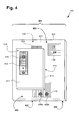
- FIG. 4 presents a perspective view showing a top side of a packaging solution including an exemplary stacked composite device, according to one implementation.
- composite device package 400 includes stacked composite device 401 formed from group III-V transistor 410 stacked over and cascoded with group IV vertical transistor 420.
- stacked composite device 401 corresponds to composite device 101, in Figure 1 .
- group III-V transistor 410 having back side 415, and drain electrode 414 including front side terminus of through-substrate via 418 on front side 413 corresponds to group III-V transistor 210, in Figures 2A and 2B . Consequently, the front side terminus of through-substrate via 418 depicted as "seen through" drain electrode 414 would in fact not be visible from the perspective of Figure 4 due to its being overlaid by drain electrode 414.
- group IV vertical transistor 420 having drain electrode 424, gate electrode 426, and gate bonding pad 412 including the upper termini of through-substrate vias 408a and 408b on top side 423, and a source electrode (not visible from the perspective of Figure 4 ) on bottom side 425, corresponds to group IV vertical transistor 320, in Figures 3A and 3B . Consequently, the top side termini of through-substrate vias 408a and 408b depicted as "seen through" gate bonding pad 412 would in fact not be visible from the perspective of Figure 4 due to their being overlaid by gate bonding pad 412.
- group III-V transistor 410 corresponds to group III-V transistor 210 and group IV vertical transistor 420 corresponds to group IV vertical transistor 320
- active die 421 of group IV vertical transistor 420 has a lateral area greater than a lateral area of active die 411 of group III-V transistor 410, as depicted in Figure 4 .
- Stacked composite device 401 includes a composite source electrode (not visible from the perspective of Figure 4 ), composite drain electrode 404, and composite gate electrode 406, corresponding respectively to composite source 102, composite drain 104, and composite gate 106 of composite device 101, in Figure 1 .
- stacked composite device 401 includes group IV vertical transistor 420 and group III-V transistor 410 stacked over group IV vertical transistor 420.
- drain electrode 424 of group IV vertical transistor 420 is in contact with a source electrode on back side 415 of group III-V transistor 410 (corresponding to source electrode 212, in Figure 2B ).
- a source electrode on bottom side 425 of group IV vertical transistor 420 (corresponding to source electrode 322, in Figure 3B ) is coupled to a gate electrode on back side 415 of group III-V transistor 410 (corresponding to gate electrode 216, in Figure 2B ) to provide a composite source electrode (provided by source electrode 322, in Figure 3B ) on bottom side 405 of stacked composite device 401.
- drain electrode 414 of group III-V transistor 410 which is electrically coupled to a drain pad on back side 415 of group III-V transistor 410 by through-substrate via 418, provides composite drain electrode 404 on top side 403 of stacked composite device 401, and gate electrode 426 of group IV vertical transistor 420 provides composite gate electrode 406 on top side 403 of stacked composite device 401.
- stacked composite device 401 may be formed by stacking back side 415 of group III-V transistor 410 directly on top of drain electrode 424 and gate bonding pad 412 of group IV vertical transistor 420, for example.
- active die 411 can be aligned such that the source electrode of group III-V transistor 410 corresponding to source electrode 212 makes direct contact with drain electrode 424 of group IV vertical transistor 420, and such that the gate electrode of group III-V transistor 410 corresponding to gate electrode 216 makes direct contact with gate bonding pad 412 of group IV vertical transistor 420.
- the gate electrode of group III-V transistor 410 corresponding to gate electrode 216 is coupled to the source electrode of group IV vertical transistor 420 at bottom side 405 of stacked composite device 401 by gate bonding pad 412 and through-substrate vias 408a and 408b, which may be TSVs, as noted above.
- the source electrode on bottom side 425 of group IV vertical transistor 420 and corresponding to source electrode 322, in Figure 3B can be coupled directly to the paddle of composite device package 400 (paddle not shown in Figure 4 ).
- Figure 5 presents a perspective view showing a top side of a packaging solution including an exemplary stacked composite device, according to another implementation.
- composite device package 500 includes stacked composite device 501 formed from group III-V transistor 510 stacked over and cascoded with group IV vertical transistor 520. It is noted that stacked composite device 501 corresponds to composite device 101, in Figure 1 .
- group III-V transistor 510 having back side 515, and drain electrode 514 including front side terminus of through-substrate via 518 on front side 513 corresponds to group III-V transistor 210, in Figures 2A and 2B , as well as to group III-V transistor 410, in Figure 4 .
- Group IV vertical transistor 520 having drain electrode 524, gate electrode 526, and gate bonding pad 512 on top side 523, and a source electrode (not visible from the perspective of Figure 5 ) on bottom side 525, corresponds in general to group IV vertical transistor 320, in Figures 3A and 3B , as well as to group IV vertical transistor 420, in Figure 4 .
- gate bonding pad 512 is electrically coupled to the source electrode on bottom side 525 of group IV vertical transistor 520 by one or more bond wires 508 and conductive tab 528.
- group III-V transistor 510 corresponds to group III-V transistor 210 and group IV vertical transistor 520 corresponds in general to group IV vertical transistor 320
- active die 521 of group IV vertical transistor 520 has a lateral area greater than a lateral area of active die 511 of group III-V transistor 510, as depicted in Figure 5 .
- Stacked composite device 501 includes a composite source electrode (not visible from the perspective of Figure 5 ), composite drain electrode 504, and composite gate electrode 506, corresponding respectively to composite source 102, composite drain 104, and composite gate 106 of composite device 101, in Figure 1 .
- stacked composite device 501 includes group IV vertical transistor 520 and group III-V transistor 510 stacked over group IV vertical transistor 520.
- drain electrode 524 of group IV vertical transistor 520 is in contact with a source electrode on back side 515 of group III-V transistor 510 (corresponding to source electrode 212, in Figure 2B ).
- a source electrode on bottom side 525 group IV vertical transistor 520 (corresponding to source electrode 322, in Figure 3B ) is coupled to a gate electrode on back side 515 of group III-V transistor 510 (corresponding to gate electrode 216, in Figure 2B ) to provide a composite source electrode (provided by source electrode 322, in Figure 3B ) on bottom side 505 of composite device package 500.
- drain electrode 514 of group III-V transistor 510 which is electrically coupled to a drain pad on back side 415 of group III-V transistor 410 by through-substrate via 418, provides composite drain electrode 504 on top side 503 of composite device package 500, and gate electrode 526 of group IV vertical transistor 520 provides composite gate electrode 506 on top side 503 of composite device package 500.
- stacked composite device 501 may be formed by stacking back side 515 of group III-V transistor 510 directly on top of drain electrode 524 and gate bonding pad 512 of group IV vertical transistor 520, for example.
- active die 511 can be aligned such that the source electrode of group III-V transistor 510 corresponding to source electrode 212 makes direct contact with drain electrode 524 of group IV vertical transistor 520, and such that the gate electrode of group III-V transistor 510 corresponding to gate electrode 216 makes direct contact with gate bonding pad 512 of group IV vertical transistor 520.
- the gate electrode of group III-V transistor 510 corresponding to gate electrode 216 is coupled to the source electrode of group IV vertical transistor 520 at bottom side 505 of stacked composite device 501 by gate bonding pad 512, one or more bond wires 508, and conductive tab 528.
- gate bonding pad 512 is shown to be coupled to the source electrode on bottom side 525 of group IV vertical transistor 520 through one or more bond wires 508, such as gold (Au) or copper (Cu) bond wires, for example, in other implementations one or more bond wires 508 may be replaced by conductive ribbons, conductive metal clips, or other connectors comprising conductive materials such as Al, Au, Cu, and/or other metals or composite materials. It is reiterated that the features and characteristics represented by the specific example shown in Figure 5 are depicted in detail merely as a conceptual aid, and are not to be interpreted as limitations.
- Stacking of group III-V transistor 410/510 on top of group IV vertical transistor 420/520 may be achieved using, for example, solder, conductive adhesive, conductive tape, sintering, or other attachment methods, resulting in formation of a direct mechanical contact between group IV vertical transistor 420/520 and group III-V transistor 410/510.
- Such direct attachment of group IV vertical transistor 420/520 to group III-V transistor 410/510 can advantageously reduce parasitic inductance and resistance, improve thermal dissipation, and reduce form factor and manufacturing cost compared to conventional packaging solutions.
- active die 411/511 of group III-V transistor 410/510 and/or active die 421/521 of group IV vertical transistor 420/520 may be thinned so as to have a die thickness in a range from approximately thirty microns (30 ⁇ m) to approximately sixty microns (60 ⁇ m) to enhance thermal conductivity.
Landscapes
- Junction Field-Effect Transistors (AREA)
Abstract
Description
- The present application claims the benefit of and priority to a pending provisional application entitled "Group III-Nitride and Group IV Composite Device," Serial No.
61/473,907 filed on April 11, 2011 - As used herein, the phrase "group III-V" refers to a compound semiconductor including at least one group III element and at least one group V element. By way of example, a group III-V semiconductor may take the form of a III-Nitride semiconductor. "III-Nitride" or "III-N" refers to a compound semiconductor that includes nitrogen and at least one group III element including aluminum (Al), gallium (Ga), indium (In), and boron (B), and including but not limited to any of its alloys, such as aluminum gallium nitride (AlxGa(1-x)N), indium gallium nitride (InyGa(1-y)N), aluminum indium gallium nitride (AlxInyGa(1-x-y)N), gallium arsenide phosphide nitride (GaAsaPbN(1-a-b)), aluminum indium gallium arsenide phosphide nitride (AlxInyGa(1-x-y)AsaPbN(1-a-b)), for example. III-Nitride also refers generally to any polarity including but not limited to Ga-polar, N-polar, semi-polar or non-polar crystal orientations. A III-Nitride material may also include either the Wurtzitic, Zincblende or mixed polytypes, and may include single-crystal, monocrystalline, polycrystalline, or amorphous structures.
- Also as used herein, the phrase "group IV" refers to a semiconductor that includes at least one group four element including silicon (Si), germanium (Ge) and carbon (C), and also includes compound semiconductors such as silicon germanium (SiGe) and silicon carbide (SiC), for example. Group IV also refers to semiconductor materials which include more than one layer of group IV elements, or doping of group IV elements to produce strained group IV material, and may also include group IV based composite substrates such as silicon on insulstor (SOI), separation by implantation of oxygen (SIMOX) process substrates, and silicon on sapphire (SOS), for example.
- Moreover, and as also used herein, the phrase "LV device" refers to a low-voltage device. Typical voltage ratings include LV ∼ 0V-50V, midvoltage (MV) ∼ 50V-300V, and high-voltage (HV) ∼ 300V-1200V.
- In high power and high performance circuit applications, III-Nitride transistors, such as gallium nitride (GaN) field-effect transistors (FETs) and high mobility electron transistors (HEMTs), are often desirable for their high efficiency and high-voltage operation. Moreover, it is often desirable to combine such III-Nitride transistors with other FETs, such as silicon FETs, to create high performance composite switching devices.
- In power management applications where normally OFF characteristics of power devices are desirable, a depletion mode (normally ON) III-Nitride transistor can be cascoded with an enhancement mode (normally OFF) low-voltage (LV) or midvoltage (MV) group IV semiconductor transistor, for example a silicon FET, to produce an enhancement mode (normally OFF) composite power device. However, conventional packaging techniques for combining III-Nitride transistors with silicon FETs, for example, often counterweigh the benefits provided by III-Nitride devices. For instance, conventional package designs may place discrete components side-by-side on a common support surface implemented using a ceramic based substrate such as a direct bonded copper (DBC) substrate, or a ceramic substrate on a lead-frame. Such side-by-side configuration can undesirably increase the parasitic inductance and resistance in the current paths of the composite power device, and would also increase the thermal dissipation requirements of the package. Moreover, the side-by-side placement of devices on a common substrate can undesirably increase package form factor, as well as manufacturing costs.
- The present disclosure is directed to a stacked composite device including a group III-V transistor and a group IV vertical transistor, substantially as shown in and/or described in connection with at least one of the figures, and as set forth more completely in the claims.
-
-
Figure 1 presents a diagram representative of one exemplary implementation of a composite device. -
Figure 2A presents a perspective view showing a front side of an exemplary group III-V transistor suitable for use in a stacked composite device, according to one implementation. -
Figure 2B presents a perspective view showing a back side of the exemplary group III-V transistor shown inFigure 2A . -
Figure 3A presents a perspective view showing a top side of an exemplary group IV vertical transistor suitable for use in a stacked composite device, according to one implementation. -
Figure 3B presents a perspective view showing a bottom side of the exemplary group IV vertical transistor shown inFigure 3A . -
Figure 4 presents a perspective view showing a top side of an exemplary stacked composite device implemented using the transistors shown byFigures 2A, 2B ,3A , and3B . -
Figure 5 presents a perspective view showing a top side of an exemplary stacked composite device, according to another implementation. - The following description contains specific information pertaining to implementations in the present disclosure. One skilled in the art will recognize that the present disclosure may be implemented in a manner different from that specifically discussed herein. The drawings in the present application and their accompanying detailed description are directed to merely exemplary implementations. Unless noted otherwise, like or corresponding elements among the figures may be indicated by like or corresponding reference numerals. Moreover, the drawings and illustrations in the present application are generally not to scale, and are not intended to correspond to actual relative dimensions.
- III-Nitride materials include, for example, gallium nitride (GaN) and its alloys such as aluminum gallium nitride (AlGaN), indium gallium nitride (InGaN), and aluminum indium gallium nitride (AlInGaN). These materials are semiconductor compounds that have a relatively wide, direct bandgap and strong piezoelectric polarizations, and can enable high breakdown fields, high saturation velocities, and the creation of two-dimensional electron gases (2DEGs). As a result, III-Nitride materials such as GaN are used in many microelectronic applications as depletion mode (e.g., normally ON) and enhancement mode (e.g., normally OFF) power field-effect transistors (FETs) and high electron mobility transistors (HEMTs), for example.
- In power management applications where normally OFF characteristics of power devices are required, a depletion mode III-Nitride or other group III-V device can be cascoded with a low-voltage (LV) or midvoltage (MV) group IV semiconductor device to produce an enhancement mode composite power device. However, the utility and reliability of such a composite device can be compromised by conventional packaging techniques for combining III-Nitride transistors with silicon or other group IV semiconductor FETs, which can often negate the benefits provided by III-Nitride devices. For example, and as noted above, conventional package designs may place discrete components side-by-side on a common support surface implemented using a ceramic based substrate such as a direct bonded copper (DBC) substrate, or a ceramic substrate on a lead-frame. Such side-by-side configuration can undesirably increase the parasitic inductance and resistance in the current paths of the composite power device, and would also increase the thermal dissipation requirements of the package. Moreover, the side-by-side placement of devices on a common substrate can undesirably increase package form factor, as well as manufacturing costs. As a result, a compact and cost-effective packaging solution for integrating III-Nitride or other group III-V transistors with group IV FETs, such as silicon FETs, is needed.
- One approach to providing the needed packaging solution is implemented by the vertical stacking of the silicon or other group IV active die on top of the III-Nitride or other group III-V active die, as disclosed in
U.S. Patent Application Number 13/053,646 , entitled "III-Nitride Transistor Stacked with Diode in a Package," filed on March 22, 2011; as well as inU.S. Patent Application Number 13/053,556 , entitled: "III-Nitride Transistor Stacked with FET in a Package," also filed on March 22, 2011, both of which are hereby incorporated by reference in their entirety. - The present application is directed to a stacked composite device wherein the group III-V active die is stacked on top of a silicon or group IV active die having a vertical transistor formed therein. The present approach is motivated in part by the larger die size typically required for the bottom die. That is to say, by implementing the bottom (larger) active die of the composite device using a less expensive group IV material such as silicon, and stacking a smaller active die formed of a costlier group III-V material such as GaN over the smaller group IV active die, the present application discloses a compact, cost effective packaging solution advantageously providing the performance advantages enabled by group III-V transistors.
- According to one implementation, the stacked composite device may include a III-Nitride power transistor cascoded with an LV or MV group IV vertical transistor. The cascoded combination of the III-Nitride power transistor, which may be a normally ON device, for example, with the LV or MV group IV vertical transistor can be implemented to produce a normally OFF composite power device. Moreover, the composite device configurations disclosed by the present application are designed to substantially reduce parasitic inductance and resistance, and enhance thermal dissipation by a composite device package when compared to conventional integrated packaging solutions.
- Referring to
Figure 1, Figure 1 shows one exemplary implementation of a composite device. As shown inFigure 1 ,composite device 101 includes group III-V transistor 110 cascoded with group IVtransistor 120. Also shown inFigure 1 arecomposite source 102,composite drain 104, andcomposite gate 106 ofcomposite device 101, as well assource 112,drain 114, andgate 116 of group III-V transistor 110, andbody diode 121,source 122,drain 124, andgate 126 of group IVtransistor 120. - Group III-V
transistor 110 may be a III-Nitride power transistor and may be implemented as an insulated-gate FET (IGFET), or as a heterostructure FET (HFET), for example. In one implementation, group III-V transistor 110 may take the form of a metal-insulator-semiconductor FET (MISFET), such as a metal-oxide-semiconductor FET (MOSFET). Alternatively, when implemented as an HFET, group III-V transistor 110 may be a HEMT configured to produce a 2DEG. According to one implementation, for example, group III-V transistor 110 may be a high-voltage (HV) device configured to sustain a drain voltage of approximately 600V and having a gate rating of approximately 40V. It is noted that in some implementations,composite device 101 1 may utilize an insulated gate bipolar transistor (IGBT) as a power transistor in place of a group III-V FET or HEMT. It is further noted thatcomposite device 101 may utilize a group III-V FET or HEMT other than a III-N FET or HEMT, such as a III-As, III-P or III-AsaPbN(1-a-b) FET or HEMT, for example, as group III-V transistor 110. - Group IV
transistor 120 may be implemented as an LV or MV group IV vertical transistor, such as a silicon vertical transistor having a breakdown voltage in a range from approximately 25V to approximately 250V, for example. According to one implementation, group IVtransistor 120 may be a silicon vertical MISFET or MOSFET, for example. However, in other implementations,group IV transistor 120 may include any suitable group IV material, such as silicon carbide (SiC), germanium (Ge), silicon germanium (SiGe), or a strained group IV element or compound, for example. - The cascoded combination of group III-
V transistor 110 andgroup IV transistor 120 producescomposite device 101, which according to the implementation shown inFigure 1 results in a composite three terminal device functioning in effect as a composite transistor havingcomposite source 102 andcomposite gate 106 provided bygroup IV transistor 120, andcomposite drain 104 provided by group III-V transistor 110. Moreover, and as will be described in greater detail by reference to the exemplary implementations discussed below,composite device 101 may be configured so as to be contained by a compact package having reduced parasitic inductance and resistance, and enhanced thermal dissipation. - Continuing to
Figures 2A and 2B, Figure 2A presents a perspective view showingfront side 213 of exemplary group III-V transistor 210 suitable for use in a stacked composite device, according to one implementation, whileFigure 2B presents a perspective view showing backside 215 of group III-V transistor 210. As shown byFigure 2A , group III-V transistor 210 includesactive die 211 havinglateral area 217 and includingdrain electrode 214 formed onfront side 213 ofactive die 211. Also shown inFigure 2A is front side terminus of through-substrate via 218 electricallycoupling drain electrode 214 to drainpad 219 onback side 215 of active die 211 (drain pad 219 and back side terminus of through-substrate via 218 shown inFigure 2B ). As further shown byFigure 2B ,source electrode 212,gate electrode 216, anddrain pad 219 including back side terminus of through-substrate via 218 are formed onback side 215 ofactive die 211. It is noted that although the front side terminus of through-substrate via 218 is visually depicted as "seen through"drain electrode 214 in the interests of conceptual clarity, in practice the front side terminus of through-substrate via 218 would be obscured by the presence ofdrain electrode 214 and thus would not be visible from the perspective view shown byFigure 2A . Similarly, the back side terminus of through-substrate via 218 visually depicted as "seen through"drain pad 219 onback side 215 ofactive die 211 would be obscured by the presence ofdrain pad 219 and thus would not be visible from the perspective view shown byFigure 2B . -
Active die 211 may be formed of a III-Nitride material, for example, and may be implemented as a HEMT power device. As noted above,drain pad 219 is coupled to drainelectrode 214 by through-substrate via 218. Group III-V transistor 210 havingsource electrode 212,drain electrode 214, andgate electrode 216 corresponds to group III-V transistor 110 havingsource 112, drain 114, andgate 116, inFigure 1 , and may share any of the characteristics previously attributed to that corresponding device above. - Moving to
Figure 3A, Figure 3A presents a perspective view showingtop side 323 of exemplary group IVvertical transistor 320 suitable for use in a stacked composite device, according to one implementation. As shown byFigure 3A , group IVvertical transistor 320 includesactive die 321, which may be formed of any suitable group IV semiconductor, and includesdrain electrode 324,gate electrode 326, andgate bonding pad 312 for receiving a gate electrode of a stacked group III-V transistor (corresponding togate electrode 216, inFigure 2B ), ontop side 323 ofactive die 321. Also shown inFigure 3A are top side termini of through-substrate vias gate bonding pad 312 to a source electrode of group IV vertical transistor 320 (source electrode not visible from the perspective ofFigure 3A ) onbottom side 325 ofactive die 321. Group IVvertical transistor 320 may be implemented as a group IV vertical FET, such as a silicon vertical FET, for example. In addition,Figure 3A showslateral area 327 ofactive die 321. It is noted thatlateral area 327 ofactive die 321 is greater thanlateral area 217 ofactive die 211, inFigures 2A and 2B . - Continuing to
Figure 3B, Figure 3B presents a perspective view showingbottom side 325 of exemplary group IVvertical transistor 320, consistent with the implementation shown byFigure 3A . As shown byFigure 3B ,source electrode 322 of group IVvertical transistor 320 is formed onbottom side 325active die 321. Also shown inFigure 3B are bottom side termini of through-substrate vias Figure 3A . As was true for the representation shown inFigure 2A , it is noted that although the top side termini of through-substrate vias gate bonding pad 312 in the interests of conceptual clarity, in practice the top side termini of through-substrate vias gate bonding pad 312 and thus would not be visible from the perspective view shown byFigure 3A . Similarly, the bottom side termini of through-substrate vias source electrode 322 onbottom side 325 ofactive die 321 would be obscured by the presence ofsource electrode 322 and thus would not be visible from the perspective view shown byFigure 3B . - Referring now to
Figure 4, Figure 4 presents a perspective view showing a top side of a packaging solution including an exemplary stacked composite device, according to one implementation. As shown inFigure 4 ,composite device package 400 includes stackedcomposite device 401 formed from group III-V transistor 410 stacked over and cascoded with group IVvertical transistor 420. It is noted that stackedcomposite device 401 corresponds tocomposite device 101, inFigure 1 . In addition, group III-V transistor 410 having backside 415, anddrain electrode 414 including front side terminus of through-substrate via 418 onfront side 413, corresponds to group III-V transistor 210, inFigures 2A and 2B . Consequently, the front side terminus of through-substrate via 418 depicted as "seen through"drain electrode 414 would in fact not be visible from the perspective ofFigure 4 due to its being overlaid bydrain electrode 414. - Moreover, group IV
vertical transistor 420 havingdrain electrode 424,gate electrode 426, andgate bonding pad 412 including the upper termini of through-substrate vias top side 423, and a source electrode (not visible from the perspective ofFigure 4 ) onbottom side 425, corresponds to group IVvertical transistor 320, inFigures 3A and3B . Consequently, the top side termini of through-substrate vias gate bonding pad 412 would in fact not be visible from the perspective ofFigure 4 due to their being overlaid bygate bonding pad 412. It is further noted that insofar as group III-V transistor 410 corresponds to group III-V transistor 210 and group IVvertical transistor 420 corresponds to group IVvertical transistor 320, active die 421 of group IVvertical transistor 420 has a lateral area greater than a lateral area ofactive die 411 of group III-V transistor 410, as depicted inFigure 4 . - Stacked
composite device 401 includes a composite source electrode (not visible from the perspective ofFigure 4 ),composite drain electrode 404, andcomposite gate electrode 406, corresponding respectively tocomposite source 102,composite drain 104, andcomposite gate 106 ofcomposite device 101, inFigure 1 . As shown inFigure 4 , stackedcomposite device 401 includes group IVvertical transistor 420 and group III-V transistor 410 stacked over group IVvertical transistor 420. According to the implementation shown inFigure 4 ,drain electrode 424 of group IVvertical transistor 420 is in contact with a source electrode onback side 415 of group III-V transistor 410 (corresponding to sourceelectrode 212, inFigure 2B ). In addition, a source electrode onbottom side 425 of group IV vertical transistor 420 (corresponding to sourceelectrode 322, inFigure 3B ) is coupled to a gate electrode onback side 415 of group III-V transistor 410 (corresponding togate electrode 216, inFigure 2B ) to provide a composite source electrode (provided bysource electrode 322, inFigure 3B ) onbottom side 405 of stackedcomposite device 401. Moreover,drain electrode 414 of group III-V transistor 410, which is electrically coupled to a drain pad onback side 415 of group III-V transistor 410 by through-substrate via 418, providescomposite drain electrode 404 ontop side 403 of stackedcomposite device 401, andgate electrode 426 of group IVvertical transistor 420 providescomposite gate electrode 406 ontop side 403 of stackedcomposite device 401. - In
Figure 4 , stackedcomposite device 401 may be formed by stacking backside 415 of group III-V transistor 410 directly on top ofdrain electrode 424 andgate bonding pad 412 of group IVvertical transistor 420, for example. In that implementation,active die 411 can be aligned such that the source electrode of group III-V transistor 410 corresponding to sourceelectrode 212 makes direct contact withdrain electrode 424 of group IVvertical transistor 420, and such that the gate electrode of group III-V transistor 410 corresponding togate electrode 216 makes direct contact withgate bonding pad 412 of group IVvertical transistor 420. In this implementation, the gate electrode of group III-V transistor 410 corresponding togate electrode 216 is coupled to the source electrode of group IVvertical transistor 420 atbottom side 405 of stackedcomposite device 401 bygate bonding pad 412 and through-substrate vias bottom side 425 of group IVvertical transistor 420 and corresponding to sourceelectrode 322, inFigure 3B , can be coupled directly to the paddle of composite device package 400 (paddle not shown inFigure 4 ). - With respect to the exemplary stacked composite device implementation shown in
Figure 4 , the present inventors emphasize that the features and characteristics represented by that specific example are depicted in detail merely as a conceptual aid, and are not to be interpreted as limitations. It is noted that implementational details such as dimensions, and device layouts, for example, may be highly dependent upon the particular devices being utilized and the particular purpose for which the stacked composite device is designed. Consequently, the inventive principles illuminated by the specific example shown byFigure 4 are capable of considerable implementational variation without departing from the scope of the inventive concepts disclosed herein. - Moving to
Figure 5, Figure 5 presents a perspective view showing a top side of a packaging solution including an exemplary stacked composite device, according to another implementation. As shown inFigure 5 ,composite device package 500 includes stackedcomposite device 501 formed from group III-V transistor 510 stacked over and cascoded with group IVvertical transistor 520. It is noted that stackedcomposite device 501 corresponds tocomposite device 101, inFigure 1 . In addition, group III-V transistor 510 having backside 515, anddrain electrode 514 including front side terminus of through-substrate via 518 onfront side 513, corresponds to group III-V transistor 210, inFigures 2A and 2B , as well as to group III-V transistor 410, inFigure 4 . Thus, it is to be understood that although the front side terminus of through-substrate via 518 is visually depicted as "seen through"drain electrode 514 in the interests of conceptual clarity, in practice the front side terminus of through-substrate via 518 would be obscured by the presence ofdrain electrode 514 and thus would not be visible from the perspective shown byFigure 5 . - Group IV
vertical transistor 520 havingdrain electrode 524,gate electrode 526, andgate bonding pad 512 ontop side 523, and a source electrode (not visible from the perspective ofFigure 5 ) onbottom side 525, corresponds in general to group IVvertical transistor 320, inFigures 3A and3B , as well as to group IVvertical transistor 420, inFigure 4 . However, it is noted that, unlike the implementation shown inFigures 3A ,3B , and4 , in the implementation ofFigure 5 ,gate bonding pad 512 is electrically coupled to the source electrode onbottom side 525 of group IVvertical transistor 520 by one ormore bond wires 508 andconductive tab 528. It is further noted that insofar as group III-V transistor 510 corresponds to group III-V transistor 210 and group IVvertical transistor 520 corresponds in general to group IVvertical transistor 320, active die 521 of group IVvertical transistor 520 has a lateral area greater than a lateral area ofactive die 511 of group III-V transistor 510, as depicted inFigure 5 . - Stacked
composite device 501 includes a composite source electrode (not visible from the perspective ofFigure 5 ),composite drain electrode 504, andcomposite gate electrode 506, corresponding respectively tocomposite source 102,composite drain 104, andcomposite gate 106 ofcomposite device 101, inFigure 1 . As shown inFigure 5 , stackedcomposite device 501 includes group IVvertical transistor 520 and group III-V transistor 510 stacked over group IVvertical transistor 520. According to the implementation shown inFigure 4 ,drain electrode 524 of group IVvertical transistor 520 is in contact with a source electrode onback side 515 of group III-V transistor 510 (corresponding to sourceelectrode 212, inFigure 2B ). In addition, a source electrode onbottom side 525 group IV vertical transistor 520 (corresponding to sourceelectrode 322, inFigure 3B ) is coupled to a gate electrode onback side 515 of group III-V transistor 510 (corresponding togate electrode 216, inFigure 2B ) to provide a composite source electrode (provided bysource electrode 322, inFigure 3B ) onbottom side 505 ofcomposite device package 500. Moreover,drain electrode 514 of group III-V transistor 510, which is electrically coupled to a drain pad onback side 415 of group III-V transistor 410 by through-substrate via 418, providescomposite drain electrode 504 ontop side 503 ofcomposite device package 500, andgate electrode 526 of group IVvertical transistor 520 providescomposite gate electrode 506 ontop side 503 ofcomposite device package 500. - In
Figure 5 , stackedcomposite device 501 may be formed by stacking backside 515 of group III-V transistor 510 directly on top ofdrain electrode 524 andgate bonding pad 512 of group IVvertical transistor 520, for example. In that implementation,active die 511 can be aligned such that the source electrode of group III-V transistor 510 corresponding to sourceelectrode 212 makes direct contact withdrain electrode 524 of group IVvertical transistor 520, and such that the gate electrode of group III-V transistor 510 corresponding togate electrode 216 makes direct contact withgate bonding pad 512 of group IVvertical transistor 520. In this implementation, the gate electrode of group III-V transistor 510 corresponding togate electrode 216 is coupled to the source electrode of group IVvertical transistor 520 atbottom side 505 of stackedcomposite device 501 bygate bonding pad 512, one ormore bond wires 508, andconductive tab 528. - Although in the present implementation,
gate bonding pad 512 is shown to be coupled to the source electrode onbottom side 525 of group IVvertical transistor 520 through one ormore bond wires 508, such as gold (Au) or copper (Cu) bond wires, for example, in other implementations one ormore bond wires 508 may be replaced by conductive ribbons, conductive metal clips, or other connectors comprising conductive materials such as Al, Au, Cu, and/or other metals or composite materials. It is reiterated that the features and characteristics represented by the specific example shown inFigure 5 are depicted in detail merely as a conceptual aid, and are not to be interpreted as limitations. - Stacking of group III-
V transistor 410/510 on top of group IVvertical transistor 420/520 may be achieved using, for example, solder, conductive adhesive, conductive tape, sintering, or other attachment methods, resulting in formation of a direct mechanical contact between group IVvertical transistor 420/520 and group III-V transistor 410/510. Such direct attachment of group IVvertical transistor 420/520 to group III-V transistor 410/510 can advantageously reduce parasitic inductance and resistance, improve thermal dissipation, and reduce form factor and manufacturing cost compared to conventional packaging solutions. To improve thermal dissipation even further,active die 411/511 of group III-V transistor 410/510 and/oractive die 421/521 of group IVvertical transistor 420/520 may be thinned so as to have a die thickness in a range from approximately thirty microns (30 µm) to approximately sixty microns (60 µm) to enhance thermal conductivity. - From the above description it is manifest that various techniques can be used for implementing the concepts described in the present application without departing from the scope of those concepts. Moreover, while the concepts have been described with specific reference to certain implementations, a person of ordinary skill in the art would recognize that changes can be made in form and detail without departing from the spirit and the scope of those concepts. As such, the described implementations are to be considered in all respects as illustrative and not restrictive. It should also be understood that the present application is not limited to the particular implementations described herein, but many rearrangements, modifications, and substitutions are possible without departing from the scope of the present disclosure.
Claims (15)
- A stacked composite device having a composite drain, a composite source, and a composite gate, said stacked composite device comprising:a group IV vertical transistor;a group III-V transistor stacked over said group IV vertical transistor;a drain on a top side of said group IV vertical transistor being in contact with a source of said group III-V transistor;a source on a bottom side of said group IV vertical transistor being coupled to a gate of said group III-V transistor to provide said composite source on a bottom side of said stacked composite device;a drain of said group III-V transistor providing said composite drain on a top side of said stacked composite device;a gate of said group IV vertical transistor providing said composite gate on said top side of said stacked composite device.
- The stacked composite device of claim 1, wherein said source on said bottom side of said group IV vertical transistor is coupled to said gate of said group III-V transistor through at least one through-silicon via (TSV).
- The stacked composite device of claim 1, wherein said source on said bottom side of said group IV vertical transistor is coupled to said gate of said group III-V transistor through at least one bond wire.
- The stacked composite device of claim 1, wherein said group III-V transistor is a normally ON device and said stacked composite device is a normally OFF device.
- The stacked composite device of claim 1, wherein said group III-V transistor is a high-voltage transistor and said group IV vertical transistor is a low-voltage transistor.
- A composite device package comprising:a group IV vertical transistor in a first active die;a group III-V transistor stacked over said group IV vertical transistor in a second active die, a lateral area of said first active die being greater than a lateral area of said second active die;a drain on a top side of said group IV vertical transistor being in contact with a source of said group III-V transistor;a source on a bottom side of said group IV vertical transistor being coupled to a gate of said group III-V transistor to provide a composite source on a bottom side of said composite device package;a drain of said group III-V transistor providing a composite drain on a top side of said composite device package;a gate of said group IV vertical transistor providing a composite gate on said top side of said composite device package.
- The composite device package of claim 6, wherein said source on said bottom side of said group IV vertical transistor is coupled to said gate of said group III-V transistor through at least one through-silicon via (TSV).
- The composite device package of claim 6, wherein said source on said bottom side of said group IV vertical transistor is coupled to said gate of said group III-V transistor through at least one bond wire.
- The composite device package of claim 6, wherein said group III-V transistor is a normally ON device and a composite device formed of said group III-V transistor and said group IV vertical transistor is a normally OFF device.
- The composite device package of claim 6, wherein said group III-V transistor is a high-voltage transistor and said group IV vertical transistor is a low-voltage transistor.
- A stacked composite device having a composite drain, a composite source, and a composite gate, said stacked composite device comprising:a silicon vertical FET;a III-Nitride transistor stacked over said silicon vertical FET;a drain on a top side of said silicon vertical FET being in contact with a source of said III-Nitride transistor;a source on a bottom side of said silicon vertical FET being coupled to a gate of said III-Nitride transistor to provide said composite source on a bottom side of said stacked composite device;a drain of said III-Nitride transistor providing said composite drain on a top side of said stacked composite device;a gate of said silicon vertical FET providing said composite gate on said top side of said stacked composite device.
- The stacked composite device of claim 11, wherein said source on said bottom side of said silicon vertical FET is coupled to said gate of said III-Nitride transistor through at least one through-silicon via (TSV).
- The stacked composite device of claim 11, wherein said source on said bottom side of said silicon vertical FET is coupled to said gate of said III-Nitride transistor through at least one bond wire.
- The stacked composite device of claim 11, wherein said III-Nitride transistor is a normally ON device and said stacked composite device is a normally OFF device.
- The stacked composite device of claim 11, wherein said III-Nitride transistor is a high-voltage transistor and said silicon vertical FET is a low-voltage transistor.
Applications Claiming Priority (2)
| Application Number | Priority Date | Filing Date | Title |
|---|---|---|---|
| US201161473907P | 2011-04-11 | 2011-04-11 | |
| US13/434,412 US9343440B2 (en) | 2011-04-11 | 2012-03-29 | Stacked composite device including a group III-V transistor and a group IV vertical transistor |
Publications (2)
| Publication Number | Publication Date |
|---|---|
| EP2511952A1 true EP2511952A1 (en) | 2012-10-17 |
| EP2511952B1 EP2511952B1 (en) | 2017-11-15 |
Family
ID=46000798
Family Applications (1)
| Application Number | Title | Priority Date | Filing Date |
|---|---|---|---|
| EP12163106.3A Not-in-force EP2511952B1 (en) | 2011-04-11 | 2012-04-04 | Stacked composite device including a group III-V transistor and a group IV vertical transistor |
Country Status (3)
| Country | Link |
|---|---|
| US (1) | US9343440B2 (en) |
| EP (1) | EP2511952B1 (en) |
| JP (1) | JP5632416B2 (en) |
Cited By (7)
| Publication number | Priority date | Publication date | Assignee | Title |
|---|---|---|---|---|
| ITTO20121081A1 (en) * | 2012-12-14 | 2014-06-15 | St Microelectronics Srl | ELECTRONIC POWER COMPONENT NORMALLY OFF |
| EP2824838A1 (en) * | 2013-07-12 | 2015-01-14 | International Rectifier Corporation | Integrated III-Nitride D-mode HFET with cascoded pair half bridge |
| EP2811518A3 (en) * | 2013-03-21 | 2015-03-25 | Kabushiki Kaisha Toshiba | Semiconductor device |
| CN105144379A (en) * | 2013-05-28 | 2015-12-09 | 夏普株式会社 | Semiconductor device |
| WO2016071366A1 (en) * | 2014-11-04 | 2016-05-12 | Commissariat à l'énergie atomique et aux énergies alternatives | Electronic power device with vertical 3d switching cell |
| FR3059155A1 (en) * | 2016-11-23 | 2018-05-25 | Exagan | INTEGRATED CIRCUIT SHAPED WITH A STACK OF TWO CHIPS CONNECTED IN SERIES |
| EP3349358A4 (en) * | 2015-09-10 | 2019-04-17 | Furukawa Electric Co. Ltd. | ELECTRICAL DEVICE |
Families Citing this family (26)
| Publication number | Priority date | Publication date | Assignee | Title |
|---|---|---|---|---|
| US8981380B2 (en) * | 2010-03-01 | 2015-03-17 | International Rectifier Corporation | Monolithic integration of silicon and group III-V devices |
| US9219058B2 (en) * | 2010-03-01 | 2015-12-22 | Infineon Technologies Americas Corp. | Efficient high voltage switching circuits and monolithic integration of same |
| US8987833B2 (en) | 2011-04-11 | 2015-03-24 | International Rectifier Corporation | Stacked composite device including a group III-V transistor and a group IV lateral transistor |
| US9343440B2 (en) | 2011-04-11 | 2016-05-17 | Infineon Technologies Americas Corp. | Stacked composite device including a group III-V transistor and a group IV vertical transistor |
| US9129838B2 (en) * | 2011-11-24 | 2015-09-08 | Sharp Kabushiki Kaisha | Semiconductor device and electronic apparatus |
| US9362267B2 (en) * | 2012-03-15 | 2016-06-07 | Infineon Technologies Americas Corp. | Group III-V and group IV composite switch |
| US9330908B2 (en) | 2013-06-25 | 2016-05-03 | Globalfoundries Inc. | Semiconductor structure with aspect ratio trapping capabilities |
| US9257424B2 (en) | 2013-11-08 | 2016-02-09 | Infineon Technologies Austria Ag | Semiconductor device |
| US20150162832A1 (en) | 2013-12-09 | 2015-06-11 | International Rectifier Corporation | Group III-V Voltage Converter with Monolithically Integrated Level Shifter, High Side Driver, and High Side Power Switch |
| US20150162321A1 (en) | 2013-12-09 | 2015-06-11 | International Rectifier Corporation | Composite Power Device with ESD Protection Clamp |
| US9893174B2 (en) | 2014-05-21 | 2018-02-13 | Arizona Board Of Regents On Behalf Of Arizona State University | III-nitride based N polar vertical tunnel transistor |
| KR102003792B1 (en) * | 2014-09-26 | 2019-07-31 | 한국전자통신연구원 | Power device |
| US9768087B2 (en) * | 2014-10-08 | 2017-09-19 | Infineon Technologies Americas Corp. | Compact high-voltage semiconductor package |
| US9349809B1 (en) | 2014-11-14 | 2016-05-24 | International Business Machines Corporation | Aspect ratio trapping and lattice engineering for III/V semiconductors |
| JP2016162815A (en) * | 2015-02-27 | 2016-09-05 | 株式会社ジェイテクト | Semiconductor component and manufacturing method of the same |
| US10505032B2 (en) | 2015-10-30 | 2019-12-10 | The Hong Kong University Of Science And Technology | Semiconductor device with III-nitride channel region and silicon carbide drift region |
| WO2020191357A1 (en) * | 2019-03-21 | 2020-09-24 | Transphorm Technology, Inc. | Integrated design for iii-nitride devices |
| US12500562B2 (en) | 2020-04-03 | 2025-12-16 | Macom Technology Solutions Holdings, Inc. | RF amplifier devices and methods of manufacturing including modularized designs with flip chip interconnections |
| US11837457B2 (en) * | 2020-09-11 | 2023-12-05 | Wolfspeed, Inc. | Packaging for RF transistor amplifiers |
| KR20230002671A (en) | 2020-04-23 | 2023-01-05 | 가부시키가이샤 한도오따이 에네루기 켄큐쇼 | semiconductor device |
| FR3121549B1 (en) | 2021-03-30 | 2025-01-03 | Exagan | Electronic device comprising two high electron mobility transistors |
| CN217468434U (en) * | 2021-03-30 | 2022-09-20 | 埃克斯甘公司 | Electronic Devices and Electronic Packaging |
| JP7470086B2 (en) | 2021-09-13 | 2024-04-17 | 株式会社東芝 | Semiconductor Device |
| JP2023113217A (en) * | 2022-02-03 | 2023-08-16 | ルネサスエレクトロニクス株式会社 | Semiconductor devices and circuit devices |
| CN114520214B (en) * | 2022-02-11 | 2026-03-06 | 深圳市时代速信科技有限公司 | A common-source cascode transistor package structure |
| CN115579344B (en) * | 2022-08-31 | 2026-03-17 | 佛山市国星光电股份有限公司 | A power semiconductor device |
Citations (4)
| Publication number | Priority date | Publication date | Assignee | Title |
|---|---|---|---|---|
| US20070262346A1 (en) * | 2006-05-10 | 2007-11-15 | Ralf Otremba | Electronic Component and a Method for its Production |
| US20080191216A1 (en) * | 2007-02-09 | 2008-08-14 | Sanken Electric Co., Ltd. | Diode-Like Composite Semiconductor Device |
| US20090189191A1 (en) * | 2008-01-30 | 2009-07-30 | The Furukawa Electric Co., Ltd | Semiconductor device |
| US20110049580A1 (en) * | 2009-08-28 | 2011-03-03 | Sik Lui | Hybrid Packaged Gate Controlled Semiconductor Switching Device Using GaN MESFET |
Family Cites Families (42)
| Publication number | Priority date | Publication date | Assignee | Title |
|---|---|---|---|---|
| US3648131A (en) | 1969-11-07 | 1972-03-07 | Ibm | Hourglass-shaped conductive connection through semiconductor structures |
| JPS6252954A (en) | 1985-09-02 | 1987-03-07 | Toshiba Corp | Semiconductor device |
| JP3469730B2 (en) | 1996-11-29 | 2003-11-25 | 三洋電機株式会社 | Semiconductor element |
| JP2996641B2 (en) | 1997-04-16 | 2000-01-11 | 松下電器産業株式会社 | High frequency semiconductor device and method of manufacturing the same |
| JP2002076023A (en) | 2000-09-01 | 2002-03-15 | Nec Corp | Semiconductor device |
| US6600182B2 (en) | 2001-09-26 | 2003-07-29 | Vladimir Rumennik | High current field-effect transistor |
| JP3850739B2 (en) | 2002-02-21 | 2006-11-29 | 三菱電機株式会社 | Semiconductor device |
| US7078743B2 (en) | 2003-05-15 | 2006-07-18 | Matsushita Electric Industrial Co., Ltd. | Field effect transistor semiconductor device |
| US7166867B2 (en) | 2003-12-05 | 2007-01-23 | International Rectifier Corporation | III-nitride device with improved layout geometry |
| JP4645313B2 (en) | 2005-06-14 | 2011-03-09 | 富士電機システムズ株式会社 | Semiconductor device |
| JP2007048842A (en) | 2005-08-08 | 2007-02-22 | Toshiba Corp | Nitride semiconductor device |
| US8018056B2 (en) * | 2005-12-21 | 2011-09-13 | International Rectifier Corporation | Package for high power density devices |
| JP2007317839A (en) * | 2006-05-25 | 2007-12-06 | Sanyo Electric Co Ltd | Semiconductor device and manufacturing method thereof |
| US7501670B2 (en) | 2007-03-20 | 2009-03-10 | Velox Semiconductor Corporation | Cascode circuit employing a depletion-mode, GaN-based FET |
| JP4478175B2 (en) | 2007-06-26 | 2010-06-09 | 株式会社東芝 | Semiconductor device |
| US7972902B2 (en) | 2007-07-23 | 2011-07-05 | Samsung Electronics Co., Ltd. | Method of manufacturing a wafer including providing electrical conductors isolated from circuitry |
| US20090051043A1 (en) * | 2007-08-21 | 2009-02-26 | Spansion Llc | Die stacking in multi-die stacks using die support mechanisms |
| US7911066B2 (en) | 2007-08-29 | 2011-03-22 | Agilent Technologies, Inc. | Through-chip via interconnects for stacked integrated circuit structures |
| US7800208B2 (en) | 2007-10-26 | 2010-09-21 | Infineon Technologies Ag | Device with a plurality of semiconductor chips |
| JP5130906B2 (en) * | 2007-12-26 | 2013-01-30 | サンケン電気株式会社 | Switch device |
| US8101996B2 (en) | 2008-04-15 | 2012-01-24 | Fairchild Semiconductor Corporation | Three-dimensional semiconductor device structures and methods |
| JP4600576B2 (en) | 2008-05-08 | 2010-12-15 | 株式会社デンソー | Semiconductor device and manufacturing method thereof |
| KR100997272B1 (en) | 2008-07-17 | 2010-11-29 | 주식회사 동부하이텍 | Semiconductor chip and semiconductor chip stack package |
| US8513119B2 (en) | 2008-12-10 | 2013-08-20 | Taiwan Semiconductor Manufacturing Company, Ltd. | Method of forming bump structure having tapered sidewalls for stacked dies |
| US7943428B2 (en) | 2008-12-24 | 2011-05-17 | International Business Machines Corporation | Bonded semiconductor substrate including a cooling mechanism |
| JP2010244977A (en) | 2009-04-09 | 2010-10-28 | Renesas Electronics Corp | Semiconductor device |
| US7960242B2 (en) * | 2009-04-14 | 2011-06-14 | Monolithic 3D Inc. | Method for fabrication of a semiconductor device and structure |
| TWI471977B (en) | 2009-05-15 | 2015-02-01 | 精材科技股份有限公司 | Power MOS half field effect transistor package |
| US7915645B2 (en) * | 2009-05-28 | 2011-03-29 | International Rectifier Corporation | Monolithic vertically integrated composite group III-V and group IV semiconductor device and method for fabricating same |
| US8264065B2 (en) | 2009-10-23 | 2012-09-11 | Synopsys, Inc. | ESD/antenna diodes for through-silicon vias |
| US8816497B2 (en) | 2010-01-08 | 2014-08-26 | Transphorm Inc. | Electronic devices and components for high efficiency power circuits |
| US20120193785A1 (en) | 2011-02-01 | 2012-08-02 | Megica Corporation | Multichip Packages |
| US8847408B2 (en) | 2011-03-02 | 2014-09-30 | International Rectifier Corporation | III-nitride transistor stacked with FET in a package |
| US8963338B2 (en) | 2011-03-02 | 2015-02-24 | International Rectifier Corporation | III-nitride transistor stacked with diode in a package |
| US20130175542A1 (en) | 2011-04-11 | 2013-07-11 | International Rectifier Corporation | Group III-V and Group IV Composite Diode |
| US20120256190A1 (en) | 2011-04-11 | 2012-10-11 | International Rectifier Corporation | Stacked Composite Device Including a Group III-V Transistor and a Group IV Diode |
| US8987833B2 (en) | 2011-04-11 | 2015-03-24 | International Rectifier Corporation | Stacked composite device including a group III-V transistor and a group IV lateral transistor |
| US9343440B2 (en) | 2011-04-11 | 2016-05-17 | Infineon Technologies Americas Corp. | Stacked composite device including a group III-V transistor and a group IV vertical transistor |
| US20120274366A1 (en) | 2011-04-28 | 2012-11-01 | International Rectifier Corporation | Integrated Power Stage |
| EP2639832A3 (en) | 2012-03-15 | 2015-08-05 | International Rectifier Corporation | Group III-V and group IV composite diode |
| US9362267B2 (en) | 2012-03-15 | 2016-06-07 | Infineon Technologies Americas Corp. | Group III-V and group IV composite switch |
| US9041067B2 (en) | 2013-02-11 | 2015-05-26 | International Rectifier Corporation | Integrated half-bridge circuit with low side and high side composite switches |
-
2012
- 2012-03-29 US US13/434,412 patent/US9343440B2/en active Active
- 2012-04-04 EP EP12163106.3A patent/EP2511952B1/en not_active Not-in-force
- 2012-04-06 JP JP2012087821A patent/JP5632416B2/en not_active Expired - Fee Related
Patent Citations (4)
| Publication number | Priority date | Publication date | Assignee | Title |
|---|---|---|---|---|
| US20070262346A1 (en) * | 2006-05-10 | 2007-11-15 | Ralf Otremba | Electronic Component and a Method for its Production |
| US20080191216A1 (en) * | 2007-02-09 | 2008-08-14 | Sanken Electric Co., Ltd. | Diode-Like Composite Semiconductor Device |
| US20090189191A1 (en) * | 2008-01-30 | 2009-07-30 | The Furukawa Electric Co., Ltd | Semiconductor device |
| US20110049580A1 (en) * | 2009-08-28 | 2011-03-03 | Sik Lui | Hybrid Packaged Gate Controlled Semiconductor Switching Device Using GaN MESFET |
Cited By (15)
| Publication number | Priority date | Publication date | Assignee | Title |
|---|---|---|---|---|
| ITTO20121081A1 (en) * | 2012-12-14 | 2014-06-15 | St Microelectronics Srl | ELECTRONIC POWER COMPONENT NORMALLY OFF |
| EP2811518A3 (en) * | 2013-03-21 | 2015-03-25 | Kabushiki Kaisha Toshiba | Semiconductor device |
| US9123536B2 (en) | 2013-03-21 | 2015-09-01 | Kabushiki Kaisha Toshiba | Semiconductor device |
| CN105144379A (en) * | 2013-05-28 | 2015-12-09 | 夏普株式会社 | Semiconductor device |
| US9406674B2 (en) | 2013-07-12 | 2016-08-02 | Infineon Technologies Americas Corp. | Integrated III-nitride D-mode HFET with cascoded pair half bridge |
| EP2824838A1 (en) * | 2013-07-12 | 2015-01-14 | International Rectifier Corporation | Integrated III-Nitride D-mode HFET with cascoded pair half bridge |
| WO2016071366A1 (en) * | 2014-11-04 | 2016-05-12 | Commissariat à l'énergie atomique et aux énergies alternatives | Electronic power device with vertical 3d switching cell |
| US10083942B2 (en) | 2014-11-04 | 2018-09-25 | Commissariat A L'energie Atomique Et Aux Energies Alternatives | Electronic power device with vertical 3D switching cell |
| EP3349358A4 (en) * | 2015-09-10 | 2019-04-17 | Furukawa Electric Co. Ltd. | ELECTRICAL DEVICE |
| FR3059155A1 (en) * | 2016-11-23 | 2018-05-25 | Exagan | INTEGRATED CIRCUIT SHAPED WITH A STACK OF TWO CHIPS CONNECTED IN SERIES |
| WO2018096245A1 (en) * | 2016-11-23 | 2018-05-31 | Exagan | Integrated circuit formed from a stack of two series-connected chips |
| KR20190082892A (en) * | 2016-11-23 | 2019-07-10 | 엑사간 | An integrated circuit formed of a stack of two series-connected chips |
| CN110226226A (en) * | 2016-11-23 | 2019-09-10 | 埃克斯甘公司 | The integrated circuit formed by the chip for two series connections being laminated |
| US10672746B2 (en) | 2016-11-23 | 2020-06-02 | Exagan | Integrated circuit formed from a stack of two series-connected chips |
| CN110226226B (en) * | 2016-11-23 | 2023-04-14 | 埃克斯甘公司 | An integrated circuit formed by stacking two chips connected in series |
Also Published As
| Publication number | Publication date |
|---|---|
| US9343440B2 (en) | 2016-05-17 |
| EP2511952B1 (en) | 2017-11-15 |
| JP2012222361A (en) | 2012-11-12 |
| US20120256189A1 (en) | 2012-10-11 |
| JP5632416B2 (en) | 2014-11-26 |
Similar Documents
| Publication | Publication Date | Title |
|---|---|---|
| EP2511952B1 (en) | Stacked composite device including a group III-V transistor and a group IV vertical transistor | |
| US8987833B2 (en) | Stacked composite device including a group III-V transistor and a group IV lateral transistor | |
| US9041067B2 (en) | Integrated half-bridge circuit with low side and high side composite switches | |
| US9362267B2 (en) | Group III-V and group IV composite switch | |
| US10083884B2 (en) | Compact high-voltage semiconductor package | |
| US9502398B2 (en) | Composite device with integrated diode | |
| EP2511954A1 (en) | Stacked composite device including a group III-V transistor and a group IV diode | |
| US9281388B2 (en) | Composite semiconductor device with a SOI substrate having an integrated diode | |
| US9184243B2 (en) | Monolithic composite III-nitride transistor with high voltage group IV enable switch | |
| EP2521176A1 (en) | High voltage cascoded III-nitride rectifier package comprising conductive clips between electrodes of components and the surface of a package support member | |
| US9202811B2 (en) | Cascode circuit integration of group III-N and group IV devices | |
| US20130175542A1 (en) | Group III-V and Group IV Composite Diode | |
| EP2639832A2 (en) | Group III-V and group IV composite diode | |
| US8853706B2 (en) | High voltage cascoded III-nitride rectifier package with stamped leadframe | |
| US8853707B2 (en) | High voltage cascoded III-nitride rectifier package with etched leadframe |
Legal Events
| Date | Code | Title | Description |
|---|---|---|---|
| PUAI | Public reference made under article 153(3) epc to a published international application that has entered the european phase |
Free format text: ORIGINAL CODE: 0009012 |
|
| AK | Designated contracting states |
Kind code of ref document: A1 Designated state(s): AL AT BE BG CH CY CZ DE DK EE ES FI FR GB GR HR HU IE IS IT LI LT LU LV MC MK MT NL NO PL PT RO RS SE SI SK SM TR |
|
| AX | Request for extension of the european patent |
Extension state: BA ME |
|
| 17P | Request for examination filed |
Effective date: 20130417 |
|
| 17Q | First examination report despatched |
Effective date: 20150710 |
|
| GRAP | Despatch of communication of intention to grant a patent |
Free format text: ORIGINAL CODE: EPIDOSNIGR1 |
|
| INTG | Intention to grant announced |
Effective date: 20170608 |
|
| GRAS | Grant fee paid |
Free format text: ORIGINAL CODE: EPIDOSNIGR3 |
|
| GRAA | (expected) grant |
Free format text: ORIGINAL CODE: 0009210 |
|
| RAP1 | Party data changed (applicant data changed or rights of an application transferred) |
Owner name: INFINEON TECHNOLOGIES AMERICAS CORP. |
|
| AK | Designated contracting states |
Kind code of ref document: B1 Designated state(s): AL AT BE BG CH CY CZ DE DK EE ES FI FR GB GR HR HU IE IS IT LI LT LU LV MC MK MT NL NO PL PT RO RS SE SI SK SM TR |
|
| REG | Reference to a national code |
Ref country code: CH Ref legal event code: EP Ref country code: GB Ref legal event code: FG4D Ref country code: AT Ref legal event code: REF Ref document number: 947051 Country of ref document: AT Kind code of ref document: T Effective date: 20171115 |
|
| REG | Reference to a national code |
Ref country code: IE Ref legal event code: FG4D |
|
| REG | Reference to a national code |
Ref country code: DE Ref legal event code: R096 Ref document number: 602012039687 Country of ref document: DE |
|
| REG | Reference to a national code |
Ref country code: NL Ref legal event code: MP Effective date: 20171115 |
|
| REG | Reference to a national code |
Ref country code: LT Ref legal event code: MG4D |
|
| REG | Reference to a national code |
Ref country code: AT Ref legal event code: MK05 Ref document number: 947051 Country of ref document: AT Kind code of ref document: T Effective date: 20171115 |
|
| PG25 | Lapsed in a contracting state [announced via postgrant information from national office to epo] |
Ref country code: LT Free format text: LAPSE BECAUSE OF FAILURE TO SUBMIT A TRANSLATION OF THE DESCRIPTION OR TO PAY THE FEE WITHIN THE PRESCRIBED TIME-LIMIT Effective date: 20171115 Ref country code: SE Free format text: LAPSE BECAUSE OF FAILURE TO SUBMIT A TRANSLATION OF THE DESCRIPTION OR TO PAY THE FEE WITHIN THE PRESCRIBED TIME-LIMIT Effective date: 20171115 Ref country code: FI Free format text: LAPSE BECAUSE OF FAILURE TO SUBMIT A TRANSLATION OF THE DESCRIPTION OR TO PAY THE FEE WITHIN THE PRESCRIBED TIME-LIMIT Effective date: 20171115 Ref country code: NL Free format text: LAPSE BECAUSE OF FAILURE TO SUBMIT A TRANSLATION OF THE DESCRIPTION OR TO PAY THE FEE WITHIN THE PRESCRIBED TIME-LIMIT Effective date: 20171115 Ref country code: ES Free format text: LAPSE BECAUSE OF FAILURE TO SUBMIT A TRANSLATION OF THE DESCRIPTION OR TO PAY THE FEE WITHIN THE PRESCRIBED TIME-LIMIT Effective date: 20171115 Ref country code: NO Free format text: LAPSE BECAUSE OF FAILURE TO SUBMIT A TRANSLATION OF THE DESCRIPTION OR TO PAY THE FEE WITHIN THE PRESCRIBED TIME-LIMIT Effective date: 20180215 |
|
| PG25 | Lapsed in a contracting state [announced via postgrant information from national office to epo] |
Ref country code: HR Free format text: LAPSE BECAUSE OF FAILURE TO SUBMIT A TRANSLATION OF THE DESCRIPTION OR TO PAY THE FEE WITHIN THE PRESCRIBED TIME-LIMIT Effective date: 20171115 Ref country code: BG Free format text: LAPSE BECAUSE OF FAILURE TO SUBMIT A TRANSLATION OF THE DESCRIPTION OR TO PAY THE FEE WITHIN THE PRESCRIBED TIME-LIMIT Effective date: 20180215 Ref country code: LV Free format text: LAPSE BECAUSE OF FAILURE TO SUBMIT A TRANSLATION OF THE DESCRIPTION OR TO PAY THE FEE WITHIN THE PRESCRIBED TIME-LIMIT Effective date: 20171115 Ref country code: AT Free format text: LAPSE BECAUSE OF FAILURE TO SUBMIT A TRANSLATION OF THE DESCRIPTION OR TO PAY THE FEE WITHIN THE PRESCRIBED TIME-LIMIT Effective date: 20171115 Ref country code: GR Free format text: LAPSE BECAUSE OF FAILURE TO SUBMIT A TRANSLATION OF THE DESCRIPTION OR TO PAY THE FEE WITHIN THE PRESCRIBED TIME-LIMIT Effective date: 20180216 Ref country code: RS Free format text: LAPSE BECAUSE OF FAILURE TO SUBMIT A TRANSLATION OF THE DESCRIPTION OR TO PAY THE FEE WITHIN THE PRESCRIBED TIME-LIMIT Effective date: 20171115 |
|
| PG25 | Lapsed in a contracting state [announced via postgrant information from national office to epo] |
Ref country code: DK Free format text: LAPSE BECAUSE OF FAILURE TO SUBMIT A TRANSLATION OF THE DESCRIPTION OR TO PAY THE FEE WITHIN THE PRESCRIBED TIME-LIMIT Effective date: 20171115 Ref country code: EE Free format text: LAPSE BECAUSE OF FAILURE TO SUBMIT A TRANSLATION OF THE DESCRIPTION OR TO PAY THE FEE WITHIN THE PRESCRIBED TIME-LIMIT Effective date: 20171115 Ref country code: SK Free format text: LAPSE BECAUSE OF FAILURE TO SUBMIT A TRANSLATION OF THE DESCRIPTION OR TO PAY THE FEE WITHIN THE PRESCRIBED TIME-LIMIT Effective date: 20171115 Ref country code: CY Free format text: LAPSE BECAUSE OF FAILURE TO SUBMIT A TRANSLATION OF THE DESCRIPTION OR TO PAY THE FEE WITHIN THE PRESCRIBED TIME-LIMIT Effective date: 20171115 Ref country code: CZ Free format text: LAPSE BECAUSE OF FAILURE TO SUBMIT A TRANSLATION OF THE DESCRIPTION OR TO PAY THE FEE WITHIN THE PRESCRIBED TIME-LIMIT Effective date: 20171115 |
|
| REG | Reference to a national code |
Ref country code: DE Ref legal event code: R097 Ref document number: 602012039687 Country of ref document: DE |
|
| PG25 | Lapsed in a contracting state [announced via postgrant information from national office to epo] |
Ref country code: IT Free format text: LAPSE BECAUSE OF FAILURE TO SUBMIT A TRANSLATION OF THE DESCRIPTION OR TO PAY THE FEE WITHIN THE PRESCRIBED TIME-LIMIT Effective date: 20171115 Ref country code: SM Free format text: LAPSE BECAUSE OF FAILURE TO SUBMIT A TRANSLATION OF THE DESCRIPTION OR TO PAY THE FEE WITHIN THE PRESCRIBED TIME-LIMIT Effective date: 20171115 Ref country code: PL Free format text: LAPSE BECAUSE OF FAILURE TO SUBMIT A TRANSLATION OF THE DESCRIPTION OR TO PAY THE FEE WITHIN THE PRESCRIBED TIME-LIMIT Effective date: 20171115 Ref country code: RO Free format text: LAPSE BECAUSE OF FAILURE TO SUBMIT A TRANSLATION OF THE DESCRIPTION OR TO PAY THE FEE WITHIN THE PRESCRIBED TIME-LIMIT Effective date: 20171115 |
|
| PLBE | No opposition filed within time limit |
Free format text: ORIGINAL CODE: 0009261 |
|
| STAA | Information on the status of an ep patent application or granted ep patent |
Free format text: STATUS: NO OPPOSITION FILED WITHIN TIME LIMIT |
|
| 26N | No opposition filed |
Effective date: 20180817 |
|
| PG25 | Lapsed in a contracting state [announced via postgrant information from national office to epo] |
Ref country code: MC Free format text: LAPSE BECAUSE OF FAILURE TO SUBMIT A TRANSLATION OF THE DESCRIPTION OR TO PAY THE FEE WITHIN THE PRESCRIBED TIME-LIMIT Effective date: 20171115 Ref country code: SI Free format text: LAPSE BECAUSE OF FAILURE TO SUBMIT A TRANSLATION OF THE DESCRIPTION OR TO PAY THE FEE WITHIN THE PRESCRIBED TIME-LIMIT Effective date: 20171115 |
|
| REG | Reference to a national code |
Ref country code: CH Ref legal event code: PL |
|
| REG | Reference to a national code |
Ref country code: BE Ref legal event code: MM Effective date: 20180430 |
|
| GBPC | Gb: european patent ceased through non-payment of renewal fee |
Effective date: 20180404 |
|
| REG | Reference to a national code |
Ref country code: IE Ref legal event code: MM4A |
|
| PG25 | Lapsed in a contracting state [announced via postgrant information from national office to epo] |
Ref country code: LU Free format text: LAPSE BECAUSE OF NON-PAYMENT OF DUE FEES Effective date: 20180404 |
|
| PG25 | Lapsed in a contracting state [announced via postgrant information from national office to epo] |
Ref country code: LI Free format text: LAPSE BECAUSE OF NON-PAYMENT OF DUE FEES Effective date: 20180430 Ref country code: CH Free format text: LAPSE BECAUSE OF NON-PAYMENT OF DUE FEES Effective date: 20180430 Ref country code: BE Free format text: LAPSE BECAUSE OF NON-PAYMENT OF DUE FEES Effective date: 20180430 Ref country code: GB Free format text: LAPSE BECAUSE OF NON-PAYMENT OF DUE FEES Effective date: 20180404 |
|
| PG25 | Lapsed in a contracting state [announced via postgrant information from national office to epo] |
Ref country code: FR Free format text: LAPSE BECAUSE OF NON-PAYMENT OF DUE FEES Effective date: 20180430 Ref country code: IE Free format text: LAPSE BECAUSE OF NON-PAYMENT OF DUE FEES Effective date: 20180404 |
|
| PG25 | Lapsed in a contracting state [announced via postgrant information from national office to epo] |
Ref country code: MT Free format text: LAPSE BECAUSE OF NON-PAYMENT OF DUE FEES Effective date: 20180404 |
|
| PG25 | Lapsed in a contracting state [announced via postgrant information from national office to epo] |
Ref country code: TR Free format text: LAPSE BECAUSE OF FAILURE TO SUBMIT A TRANSLATION OF THE DESCRIPTION OR TO PAY THE FEE WITHIN THE PRESCRIBED TIME-LIMIT Effective date: 20171115 |
|
| PG25 | Lapsed in a contracting state [announced via postgrant information from national office to epo] |
Ref country code: PT Free format text: LAPSE BECAUSE OF FAILURE TO SUBMIT A TRANSLATION OF THE DESCRIPTION OR TO PAY THE FEE WITHIN THE PRESCRIBED TIME-LIMIT Effective date: 20171115 Ref country code: HU Free format text: LAPSE BECAUSE OF FAILURE TO SUBMIT A TRANSLATION OF THE DESCRIPTION OR TO PAY THE FEE WITHIN THE PRESCRIBED TIME-LIMIT; INVALID AB INITIO Effective date: 20120404 |
|
| PG25 | Lapsed in a contracting state [announced via postgrant information from national office to epo] |
Ref country code: MK Free format text: LAPSE BECAUSE OF NON-PAYMENT OF DUE FEES Effective date: 20171115 |
|
| PG25 | Lapsed in a contracting state [announced via postgrant information from national office to epo] |
Ref country code: AL Free format text: LAPSE BECAUSE OF FAILURE TO SUBMIT A TRANSLATION OF THE DESCRIPTION OR TO PAY THE FEE WITHIN THE PRESCRIBED TIME-LIMIT Effective date: 20171115 Ref country code: IS Free format text: LAPSE BECAUSE OF FAILURE TO SUBMIT A TRANSLATION OF THE DESCRIPTION OR TO PAY THE FEE WITHIN THE PRESCRIBED TIME-LIMIT Effective date: 20180315 |
|
| P01 | Opt-out of the competence of the unified patent court (upc) registered |
Effective date: 20230528 |
|
| PGFP | Annual fee paid to national office [announced via postgrant information from national office to epo] |
Ref country code: DE Payment date: 20240621 Year of fee payment: 13 |
|
| REG | Reference to a national code |
Ref country code: DE Ref legal event code: R079 Ref document number: 602012039687 Country of ref document: DE Free format text: PREVIOUS MAIN CLASS: H01L0025070000 Ipc: H10D0080200000 |
|
| REG | Reference to a national code |
Ref country code: DE Ref legal event code: R119 Ref document number: 602012039687 Country of ref document: DE |
|
| PG25 | Lapsed in a contracting state [announced via postgrant information from national office to epo] |
Ref country code: DE Free format text: LAPSE BECAUSE OF NON-PAYMENT OF DUE FEES Effective date: 20251104 |