EP2512021A1 - Steuerung für einen Schaltstromwandler - Google Patents
Steuerung für einen Schaltstromwandler Download PDFInfo
- Publication number
- EP2512021A1 EP2512021A1 EP11250469A EP11250469A EP2512021A1 EP 2512021 A1 EP2512021 A1 EP 2512021A1 EP 11250469 A EP11250469 A EP 11250469A EP 11250469 A EP11250469 A EP 11250469A EP 2512021 A1 EP2512021 A1 EP 2512021A1
- Authority
- EP
- European Patent Office
- Prior art keywords
- controller
- current
- constant
- mode
- switching frequency
- Prior art date
- Legal status (The legal status is an assumption and is not a legal conclusion. Google has not performed a legal analysis and makes no representation as to the accuracy of the status listed.)
- Granted
Links
Images


Classifications
-
- H—ELECTRICITY
- H02—GENERATION; CONVERSION OR DISTRIBUTION OF ELECTRIC POWER
- H02M—APPARATUS FOR CONVERSION BETWEEN AC AND AC, BETWEEN AC AND DC, OR BETWEEN DC AND DC, AND FOR USE WITH MAINS OR SIMILAR POWER SUPPLY SYSTEMS; CONVERSION OF DC OR AC INPUT POWER INTO SURGE OUTPUT POWER; CONTROL OR REGULATION THEREOF
- H02M3/00—Conversion of DC power input into DC power output
- H02M3/22—Conversion of DC power input into DC power output with intermediate conversion into AC
- H02M3/24—Conversion of DC power input into DC power output with intermediate conversion into AC by static converters
- H02M3/28—Conversion of DC power input into DC power output with intermediate conversion into AC by static converters using discharge tubes with control electrode or semiconductor devices with control electrode to produce the intermediate AC
- H02M3/325—Conversion of DC power input into DC power output with intermediate conversion into AC by static converters using discharge tubes with control electrode or semiconductor devices with control electrode to produce the intermediate AC using devices of a triode or a transistor type requiring continuous application of a control signal
- H02M3/335—Conversion of DC power input into DC power output with intermediate conversion into AC by static converters using discharge tubes with control electrode or semiconductor devices with control electrode to produce the intermediate AC using devices of a triode or a transistor type requiring continuous application of a control signal using semiconductor devices only
- H02M3/33507—Conversion of DC power input into DC power output with intermediate conversion into AC by static converters using discharge tubes with control electrode or semiconductor devices with control electrode to produce the intermediate AC using devices of a triode or a transistor type requiring continuous application of a control signal using semiconductor devices only with automatic control of the output voltage or current, e.g. flyback converters
- H02M3/33523—Conversion of DC power input into DC power output with intermediate conversion into AC by static converters using discharge tubes with control electrode or semiconductor devices with control electrode to produce the intermediate AC using devices of a triode or a transistor type requiring continuous application of a control signal using semiconductor devices only with automatic control of the output voltage or current, e.g. flyback converters with galvanic isolation between input and output of both the power stage and the feedback loop
Definitions
- the present disclosure relates to the field of controllers for switched mode power converters, in particular, although not exclusively, to a controller for operating the switched mode power converter in a constant current mode of operation and a constant voltage mode of operation.
- SMPS switched mode power supply
- Such converters can be used to provide a maximum output current that is regulated over an output voltage range, which may be required for battery charging as used in mobile telephones, electric shavers and other handheld applications; for light emitting diode (LED) applications that can provide constant light output without dimming; for a defined maximum dissipation in the secondary diode; and for short circuit protection for wall-plug chargers with an open connector.
- SMPS switched mode power supply
- a commonly used SMPS topology that can provide mains isolation for battery chargers is the flyback converter.
- a controller for a switched mode power converter having a switch wherein the switched mode power converter can operate in a constant current and a constant voltage mode of operation, wherein the controller is configured to output a switch control signal for the switch and receive:
- Such a controller can provide an advantageous way of transitioning between the constant current mode of operation and the constant voltage mode of operation as the transition occurs for maximum values of the peak current and switching frequency, thereby defining a maximum output power of the converter. Controlling the transition in relation to output power in this way can be achieved with few additional components in a controller integrated circuit and without requiring any additional pins on the controller integrated circuit (IC).
- IC controller integrated circuit
- the constant current mode controller may be configured to generate output control signals when it is enabled. In other examples, the constant current mode controller may be configured to generate output control signals that set or modify one or both of peak current and switching frequency operational parameters when it is enabled. If the constant current mode controller is not enabled, it may be configured to generate output control signals that do not set or modify one or both of peak current and switching frequency operational parameters.
- the controller may be configured to enable the constant voltage mode controller if the output control signals of the constant current mode controller represent operation with peak current and switching frequency at maximum values. This may be in addition to, or instead of, the controller being configured to enable the constant current mode controller if the output control signals of the constant voltage mode controller represent operation with peak current and switching frequency at maximum values
- the primary peak current adjuster may be configured to provide the switch control signal such that it is configured to turn off the switch in order to provide operation with a constant peak current at the maximum value. In some embodiments, the primary peak current adjuster may not be required if the converter is controlled with a constant primary peak current.
- the switching frequency adjuster may be configured to provide the switch control signal such that it is configured to turn on the switch with a constant frequency at the maximum value. In some embodiments, the switching frequency adjuster may not be required if the converter is controlled with a constant switching frequency.
- the controller may be configured to enable the constant current controller when the output control signals of the constant voltage mode controller represent operation with the switching frequency and primary peak current are at their maximum values, and the sensed voltage input signal drops to a CC threshold level.
- the CC threshold level may be below the voltage level when the switched mode power converter is operating in constant voltage mode. In this way a transition mode is provided between the constant current mode of operation and the constant voltage mode of operation.
- the controller may be configured to operate the switched mode power converter with the maximum values for the switching frequency and primary peak current at the transition between the constant current mode of operation and the constant voltage mode of operation. In this way, a transition mode is provided whereby the maximum output power is maintained, and one of the output current and output voltage is adjusted to its constant value for subsequent operation in the appropriate constant mode
- the switched mode power converter may also operate in a regulated current mode of operation.
- the controller may comprise:
- Such a regulated current mode controller can enable the switched mode power converter to provide fold-back operation, which may be required to satisfy some standards or may be required in conditions where the output is continuously too low, such as for a short-circuit at the output.
- the constant current mode controller may be configured to generate the output control signal for the switching frequency adjuster and the output control signal for the primary peak current adjuster such that the switching frequency is adjusted for switching frequency values that are above a switching minimum value and the primary peak current is kept constant. In this way, it can be ensured that the switching frequency does not drop to an audible level, as defined by the switching minimum value.
- the constant current mode controller may be configured to generate the output control signal for the switching frequency adjuster and the output control signal for the primary peak current adjuster such that the switching frequency is kept constant at the switching minimum value and the primary peak current is adjusted when the switching frequency reaches the switching minimum value.
- it can be considered more efficient, in some embodiments computationally more economical, to adjust the switching frequency in preference to the peak current. Therefore, the switching frequency can be adjusted for higher sensed voltage levels when operating in constant current mode.
- the switching frequency adjuster may be configured to set the frequency of the switch control signal.
- the primary peak current adjuster may be configured to set the duty cycle or the on-time (because switching frequency is variable) of the switch control signal or set the sense level for the primary peak current.
- the primary peak current adjuster may be configured to adjust the peak current in accordance with the output control signal from the constant voltage controller when the switched mode power converter operates in a constant voltage mode of operation.
- the output control signal of the constant voltage mode controller may represent operation with maximum primary peak current, and the output control signal of the constant current mode controller may represent the required deduction from the maximum primary peak current value in order to operate in constant current mode.
- the primary peak current adjuster may be configured to adjust the peak current in accordance with both of the output control signal from the constant current controller and the output control signal from the constant voltage controller when the switched mode power converter operates in a constant current mode of operation.
- Such a converter can be considered advantageous as it may not be necessary to disable the constant voltage controller when operating in the constant current mode of operation.
- the primary peak current adjuster may comprise a first variable current source that is controllable by the constant voltage controller and a second variable current source that is controllable by the constant current controller.
- the first and second variable current sources may be in parallel with each other with one common output.
- the current from the second variable current source may be configured to be subtracted from the current of the first variable current source in order to adjust the primary peak current in the constant current mode of operation.
- the switching frequency adjuster may be configured to adjust the switching frequency in accordance with the output control signal from the constant voltage controller when the switched mode power converter operates in a constant voltage mode of operation.
- the switching frequency adjuster may be configured to adjust the switching frequency in accordance with both of the output control signal from the constant voltage controller and the output control signal from the constant current controller when the switched mode power converter operates in a constant current mode of operation.
- Such a converter can be considered advantageous as it may not be necessary to disable the constant voltage controller when operating in the constant current mode of operation.
- the output control signal of the constant voltage mode controller may represent operation with maximum switching frequency, and the output control signal of the constant current mode controller may represent the required deduction from the maximum switching frequency value in order to operate in constant current mode.
- the switching frequency adjuster may comprise a first variable current source that is controllable by the constant voltage controller and a second variable current source that is controllable by the constant current controller.
- the first and second variable current sources may be in parallel with each other with one common output.
- the current from the second variable current source may be configured to be subtracted from the current of the first variable current source in order to adjust the primary peak current in the constant current mode of operation.
- the constant current mode controller may be configured to provide output control signals that prevent the primary peak current from dropping to zero at a sensed voltage input of zero Volts. Such a minimum level may be used to ensure that the controller can start up correctly.
- a switched mode power converter comprising:
- the step of changing the mode of operation from the constant current mode of operation to the constant power mode of operation may be performed when the load experienced by the switched mode power converter in constant current mode of operation requires operation at maximum peak current and switching frequency values.
- the step of changing the mode of operation of the switched mode power from the constant power mode of operation to the constant voltage mode of operation may be performed when the load experienced by the switched mode power converter requires operation that generates the constant output voltage level with peak current and switching frequency below the maximum values.
- switched mode power converter comprising any controller disclosed herein.
- a battery charger comprising any switched mode power converter or controller disclosed herein.
- the computer program may be a software implementation, and the computer may be considered as any appropriate hardware, including a digital signal processor, a microcontroller, and an implementation in read only memory (ROM), erasable programmable read only memory (EPROM) or electronically erasable programmable read only memory (EEPROM), as non-limiting examples.
- the software may be an assembly program.
- the computer program may be provided on a computer readable medium, which may be a physical computer readable medium such as a disc or a memory device, or may be embodied as a transient signal.
- a transient signal may be a network download, including an internet download.
- One or more embodiments of the invention relate to a controller for a switched mode power converter.
- the controller can generate a switch control signal for the switched mode power converter such that the output of the switched mode power converter can operate in a constant current and a constant voltage mode of operation.
- the controller can process a sensed voltage input signal and a primary current input signal in order to control one or both of (i) the peak current at the primary side of the switched mode power converter; and (ii) the switching frequency in order to operate in constant current or constant voltage mode.
- the switched power converter can be controlled such that maximum values for (i) and (ii) are not exceeded at the transition between constant current mode and constant voltage mode and therefore a maximum output power is not exceeded. Transitioning between operational modes in this way can be implemented with relatively few additional integrated components, and in some embodiments without requiring an additional pin on the controller integrated circuit (IC).
- FIG. 1 illustrates a known flyback converter 100.
- the flyback converter 100 includes a controller 104, which in this example also includes the switch 104 of the flyback converter 100. Some of the components of the flyback converter 100 that are well known in the art will not be described here.
- the switch 104 is connected in series between the primary winding 106 of a transformer 108 and a sense resistor 110.
- the other terminal of the sense resistor 110 is connected to ground.
- the transformer 108 includes an auxiliary winding 112 that is used to provide a supply voltage and current to the controller 102.
- This supply current is illustrated as Isupply 124 in Figure 1 , and is provided to the VCC pin of the controller 102.
- a resistive divider comprising two resistors R1 114 and R2 116, is connected in series with the auxiliary winding 112 in order to provide a sensed voltage signal 130 to the FB pin of the controller 120.
- the sensed voltage signal 130 is provided from the junction of the two resistors R1 114, R2 116, and is representative of the output of the flyback converter due to the magnetic coupling between the auxiliary winding 112, the primary winding 106, and secondary winding 118 of the transformer 108.
- One or more embodiments disclosed herein relate to a controller 102 for a flyback converter 100 that can improve the performance of the converter 100.
- Embodiments of the invention can use little or minimal additional circuitry, and can use the maximum output power level and the sensed feedback voltage 130 at the FB pin of the controller 102 as two reference parameters for controlling the output of the converter.
- FIG. 2 illustrates a controller 200 according to an embodiment of the invention.
- the controller 200 could be part of the controller 102 of Figure 1 in order to provide a converter according to an embodiment of the invention.
- the switch is not shown as part of the controller 200 of Figure 2 , although in other embodiments a switch such as a field effect transistor (FET) could be included as part of the controller 200.
- FET field effect transistor
- the controller 200 receives a sensed voltage input signal 202, which could be the signal (V FB ) 130 provided by the resistive divider 114, 116 of Figure 1 , and a primary current input signal 204 representative of the current at the primary side of the transformer (I primary ). As shown in Figure 1 , the primary current input signal 204 can be taken as the current flowing through the sense resistor (Rsense 110) at the primary side of the transformer 108.
- the controller 200 outputs a switch control signal 206 that can be used to operate the switch of a converter.
- the sensed voltage input signal 202 is the value of V FB that has been sensed and sampled at the end of the secondary stroke near the end-of-conduction of the switching cycle.
- the sensed voltage on the FB pin which will be referred to as V FBS
- V FBS is a good representation of the secondary voltage at the output.
- V FBS may be considered as a good value because it is not significantly influenced by any ringing at the drain caused by the current commutation, it is sampled at a time with minimum forward voltage of the secondary output diode, and with minimum voltage drop across the copper resistance of tracks between components, the diode resistance, and over the equivalent series resistance (ESR) of the secondary output capacitor.
- V FBS V FBS . n s / n a .
- each switching cycle delivers an energy package of 1 ⁇ 2.L p .
- I peak 2 to the secondary winding 118 (the output) and the auxiliary winding 112 of the transformer 108 as shown in Figure 1 .
- the converter may have maximum values for I peak-max and f switch-max, which defines a maximum power that can be delivered.
- the maximum value for the primary current (I peak-max ) and switching frequency (f switch-max ) may be considered as end values of control ranges that are stored on the controller IC.
- the value for the peak primary current that is compared with I peak-max may be defined by a user in some examples by setting the value of an external sense resistor. Further details are provided below.
- the switch control signal 206 that is output by the controller 200 can be provided to the gate of a MOSFET in order to control the conductivity of the conduction channel of the MOSFET (between the drain and the source).
- the switch (not shown) may be part of the controller 200, and the controller may have two pins that correspond to each terminal of the switch (such as the drain and source pins of the controller 102 that are shown in Figure 1 ).
- the controller 200 includes a peak current adjuster 208 that can set at least one parameter of the switch control signal 206 in order to operate the switch such that the peak current through the primary side of the transformer is adjusted.
- the controller 200 also includes a switching frequency adjuster 210 that can set at least one parameter of the switch control signal 206 in order to adjust the switching frequency with which the switch is operated.
- the switching frequency adjuster 210 may be used to directly influence the frequency of the switch control signal 206, which may involve setting when the switch should be turned on, and the peak current adjuster may be used to influence the sense level for the primary peak current or on-time of the switch control signal 206, which may involve setting when the switch should be turned off.
- the peak primary current and/or switching frequency can be adjusted in order to change the output power and maintain a constant output current.
- the controller 200 includes a constant current mode controller 212 that is configured to provide control signals to the peak current adjuster 208 and switching frequency adjuster 210 when the converter is operating in a constant current mode of operation.
- the controller 200 includes a constant voltage mode controller 214 that is configured to provide control signals to the peak current adjuster 208 and switching frequency adjuster 210 when the converter is operating in a constant voltage mode of operation.
- the peak current adjuster 208 also receives the primary current input signal (I primary ) 204 such that the current through the primary side is made available to the controller 200.
- the constant voltage controller 214 provides an enable signal 218 to the constant current controller 212 indicative of whether or not the constant voltage controller 214 provides output control signals representative of operation with a maximum switching frequency and a maximum peak primary current. In this way, the transition from constant voltage mode to current mode occurs when the peak current (I peak ) and switching frequency (f switch ) are operating at their maximum values.
- the constant voltage mode controller 214 may inherently know when it is causing the peak current adjuster 208 and the switching frequency adjuster 210 to use these maximum values, and therefore can set the enable signal 218 accordingly. In this example, the constant voltage controller 214 may not require disabling when the flyback converter is operating in a constant current mode of operation.
- the sensed voltage input signal 202 is also provided to the constant current controller 212 and the constant voltage controller 214.
- the constant current controller 212 can be enabled when both (i) the sensed voltage input signal 202 is below a constant current (CC) threshold level, and (ii) the enable signal 218 is indicative of the switched mode power converter operating with maximum switching frequency and maximum peak primary current.
- the constant current mode controller 212 may provide the constant voltage controller 214 with an enable signal 220, which may be in addition to, or instead of, the enable signal 218 for the constant current controller 212.
- the constant voltage mode controller 214 provides the enable signal 218 to the constant current controller 212.
- the functionality for setting the enable signal 218 may be provided by one or both of the constant current controller 212 and the constant voltage controller 214, or may be provided by a separate component. In such examples it may be necessary to feedback the peak current value and switching frequency as the in-use values for these parameters may not be readily available.
- a flyback controller for 5W adapters for global mains input can provide a constant voltage mode of operation at 5V and a constant current mode of operation at 1 A.
- the maximum power that can be delivered can be considered as a constant power hyperbola 308. Any position on the constant power hyperbola 308 represents operation with the maximum peak primary current (I peak-max ) and maximum switching frequency (f switch-max ).
- the output power can be reduced in order to maintain a constant output current for a decreasing output voltage as the load impedance that is presented to the converter decreases. It will be appreciated from the above equations that the output power level can be reduced by decreasing (i) f switch, or (ii) I peak ; or (iii) f switch and I peak .
- V FBSCV 302 which represents the desired sampled voltage when the converter is operating in a constant voltage mode of operation
- V FBSCC 304 which represents the sampled voltage level at which the converter transitions to or from a constant current mode of operation and is an example of a CC threshold level discussed above
- UVLO 306 which represents a voltage lock out level.
- the UVLO level 306 defines a minimum value for the sampled voltage that can ensure that the controller can be supplied with sufficient voltage to operate correctly.
- a device such as a mobile telephone may change the load impedance that it presents to a power converter so that it receives an appropriate current and power in accordance with a charge level of the battery.
- the switch of the converter is operated such that the converter provides a constant output voltage level (V FBSCV 302) for current levels up until the maximum peak primary current and maximum switching frequency are reached, which is shown in Figure 3 as the maximum power hyperbola 308. That is, the output current is allowed to increase in constant voltage mode up until it is not possible to deliver any more power. At this point, identified with reference 310 in Figure 3 , the output current cannot be further increased whilst staying in constant voltage mode without exceeding the maximum power 308. At point 310 the output current level is defined by the maximum power hyperbola 308, the primary peak current and switching frequency are at their maximum values, and the output current equals the maximum power divided by the output voltage.
- the converter is controlled such that the output current and output voltage continue along the maximum power hyperbola 308 from point 310 to point 312 with an increasing current and decreasing voltage. This may be considered as a maximum power mode of operation or a transition mode of operation.
- the output current is then allowed to increase until the output voltage meets the threshold level V FBSCC 304 for switching over to a constant current mode of operation. At the threshold level V FBSCC 304, the output current has the desired constant value.
- This changeover to constant current mode is identified with reference 312 in Figure 3 and occurs when (i) the primary peak current and switching frequency are at their maximum values (and therefore maximum power is being delivered); and (ii) the sensed voltage at the end of the secondary stroke (V FBS ) is below a threshold level (V FBSCC 304).
- FIG. 3 The operation of an embodiment of the invention that is illustrated by Figure 3 provides an operation margin between the end of the constant voltage mode 310 and the start of the constant current mode 312.
- the sensed voltage (V FBS ) is regulated to a reference value V FBSCV 302.
- the constant current mode is enabled once the sensed voltage (V FBS ) drops below a marginally lower V FBSCC threshold level 304. It will be appreciated that in other embodiments, depending upon the levels of the constant voltage and constant current that are required, as well as the maximum power 308 that can be delivered, the size of the difference between V FBSCV 302 and V FBSCC 304 could be larger or smaller than illustrated in Figure 3 .
- the switching frequency f switch and/or the peak primary current I peak can be changed in order to adjust the output power.
- the contribution to the values for the switching frequency f switch and the peak primary current I peak that is made by components of the controller that relate to constant voltage operation still relates to the maximum values; components of the controller that relate to constant current operation are used to reduce the values of the switching frequency f switch and the peak primary current I peak from these maximum values.
- the switching frequency f switch is reduced and scales down with V FBS for the constant output current to be maintained.
- the switching frequency f switch may be reduced until it reaches a switching minimum level.
- a switching minimum level for the switching frequency f switch is the audible limit of the human ear, which may be considered as 20 kHz, or any value that is considered as practically inaudible
- the primary peak current I peak is reduced instead of f switch in order to maintain the constant output current level.
- I peak I out .
- L p . f switch k Ipk ⁇ V FBS
- I peak is scaled down with in order to maintain constant output current.
- the range of output voltages for which the peak primary current I peak could be adjusted is shown with reference 316 in Figure 3 .
- This threshold level UVLO 306 refers to the minimum supply voltage of the controller and is required to ensure that the controller operates correctly in steady-state operation.
- the controller may be provided as a separate integrated circuit 102 that receives its supply voltage (Vcc) from an auxiliary winding of the transformer of the converter. This supply voltage (Vcc) must be kept above a minimum value; this minimum level is called the Under Voltage Lock Out level (UVLO) of the Vcc.
- Vcc supply voltage
- UVLO Under Voltage Lock Out level
- Operation of the converter below the threshold level UVLO 306 is shown with reference 318 in Figure 3 , at which point f switch and I peak have been reduced and discontinuous conduction mode (DCM) operation is maintained.
- Operation below UVLO occurs during start-up, which is a transition situation wherein the output voltage increases from 0V to a desired level above the level 306 that is related to the UVLO level.
- the controller can prevent f switch and I peak from being reduced to zero for guaranteed start-up from 0V output voltage.
- the value for UVLO 306 may be set at a value that is lower than is likely to be required in steady-state use.
- the constant current mode can be used when a battery has relatively little charge
- the UVLO threshold value 306 may represent operation at a sensed voltage level (V FBS ) that is below the voltage level that would be required for a flat battery.
- the UVLO threshold may represent an output voltage of 1V and a flat battery would present a load that would draw a constant current at a voltage level of 2V.
- V FBSCC 304 a maximum output voltage level
- DCM discontinuous conduction mode
- BCM boundary conduction mode
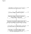
- Figure 4 shows a process flow that illustrates a method according to an embodiment of the invention.
- the method provides an example of how a controller can control a switched mode power converter as it transitions from a constant current mode of operation to a constant voltage mode of operation.
- the method starts at step 402 whereby the controller provides a switch control signal that causes the converter to operate in a constant current mode of operation.
- the output voltage may increase as the load impedance presented to the converter increases. This is step 404 of Figure 4 .
- the load impedance may be increased in this way as the charge on a battery is increased As the converter is operating in a constant current mode, it will be appreciated that the output power increases as the output voltage increases, and this can be achieved by increasing I peak , f switch , or both.
- the output power reaches a maximum value that has been defined for the converter as the values for I peak and f switch are at their maximum values.
- the controller operates the converter with the maximum values for I peak and f switch , and the output current and output voltage are allowed to change as the load continues to increase in order to maintain the maximum value of output power. As discussed above, this involves the output current and output voltage following an output power hyperbola and may be considered as a constant power mode of operation.
- the output voltage reaches the desired constant output voltage level.
- the converter operates in constant voltage mode, with a decreasing current, at step 412.
- the switch of the converter is operated such that either or both of the switching frequency (f switch ) and peak primary current (I peak ) are decreased from their maximum values.
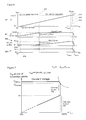
- Figure 5 illustrates a controller 500 according to an embodiment of the invention.
- Figure 6 illustrates graphically the performance of the controller 500 of Figure 5 .
- the controller receives a V FB input signal 502, which is an example of a sensed voltage input signal, and a V primary input signal 504, which is an example of a signal representative of the current in the primary winding of the transformer.
- V FB input signal 502 which is an example of a sensed voltage input signal
- V primary input signal 504 which is an example of a signal representative of the current in the primary winding of the transformer.
- the value for the peak primary current (I peak ) equals the V primary input signal 504 divided by the value of the Rsense resistor 534.
- the controller provides a switch control signal 506 to the gate of a field effect transistor 532.
- the Rsense resistor 534 that is connected between the source of the transistor 532 and ground can be a discrete component that is not part of the controller IC.
- This discrete Rsense resistor gives a design freedom for setting the maximum power as the division factor that is applied to the V primary input signal 504 in determining the peak primary current I peak can be defined by changing the resistance of the sense resistor Rsense 534.
- the components of the controller that are shown in Figure 5 are therefore connected to four pins of the controller integrated circuit (IC): FB, GND, Drain and Source. It will be appreciated from a comparison with Figure 1 that this embodiment of the invention does not need any additional pins provided on the controller IC. This is an advantageous feature of this embodiment of the invention.
- an internal sense resistor or a sense FET with an incorporated current mirror can be used instead of the discrete sense resistor Rsense 534.
- the sensed voltage input signal V FB 502 is provided to a sample and hold component 530.
- the sample and hold component 530 is configured to sense V FB 502 at the end of the secondary stroke in order to provide a sampled voltage input signal V FBS 536.
- the sampled voltage input signal V FBS 536 is provided as an input to a constant voltage (CV) controller 514.
- the CV controller 514 can process the sampled voltage input signal V FBS 536 in order to provide a control signal 510 to a switching frequency adjuster 510 and a control signal 538 to a peak current adjuster 508.
- the CV controller 514 adjusts the switching frequency and peak primary current so that the desired constant voltage is maintained during constant voltage mode.
- the switching frequency adjuster 510 includes a variable current source (I oscCV ) 548 that is adjustable by the control signal 540 from the CV controller 514.
- the current from I oscCV 548 is provided as an input to a current controlled oscillator 550.
- the output of the current controlled oscillator 550 is representative of the desired switching frequency (f switch ) and is provided to a pulse generator 552.
- the output of the pulse generator 552 is provided as the set input to an SR flip-flop 546.
- the Q output of the SR flip-flop 546 is provided as an input to a gate driver amplifier 554, and the output of the gate driver amplifier 554 is the switch control signal 506.
- Controlling the set input of the SR flip-flop 546 in this way defines the period of time between the successive transitions in the switch control signal 506 from low to high and therefore sets when the switch 532 is turned on. This period of time represents the gap between successive primary strokes of the flyback converter and therefore represents the switching frequency of the flyback converter.
- the peak current adjuster 508 includes a variable current source (I peakCV ) 542 that is adjustable by the control signal 538 from the CV controller 514.
- the current from I peakCV 542 is provided to a peak resistor Rpeak 566, such that the voltage that is dropped across Rpeak 566 is provided as an input to the inverting input of a comparator 544. This voltage is referred to as Vpeak in Figure 5 .
- the non-inverting input of the comparator 544 is provided with the voltage 504 that is dropped across the sense resistor Rsense 530 due to current at the primary side of the transformer. This input signal 504 is therefore representative of an I primary input signal.
- the output of the comparator 544 is provided to the reset input of the SR flip-flop 546 in order to control when the switch control signal 506 goes low and therefore the proportion of the switching period for which a current is allowed to flow through the primary winding of the flyback converter. In this way, the peak current adjuster 508 sets when the switch is turned off.
- the graphs can be considered as illustrative of the performance of the converter as a battery is being charged and the load presented at the output of the converter changes. It can be seen that for operation of the converter for V FBS values between the two dashed lines 610, 612, the output voltage (graph 602) is constant, and the peak primary current (represented by graph 604), switching frequency (graph 606) and output current (graph 608) gradually increase. It will be appreciated that the peak primary current (graph 604) and switching frequency (graph 606) do not necessarily need to be increased linearly to maintain a constant output voltage.
- the CV controller 514 can ensure that the peak primary current and switching frequency are not increased to a value above their maximum values by keeping the respective control signals 538, 540 below maximum values. Operating with maximum values for the peak primary current and switching frequency causes the converter to provide a maximum power output. When the current drawn by the load of the converter increases such that the control signals 538, 540 are at their maximum values, the control signals are fixed at their maximum values and an EnableCC signal 556 that is output by the CV controller 514 is set.
- a constant current (CC) controller 512 receives the EnableCC signal 556 from the CV controller 514.
- the CC controller 512 also receives the V FBS signal 536 from the sample and hold component 530.
- the CC controller 512 is configured to provide control signals 558, 560 to the peak current adjuster 508 and switching frequency adjuster 510 in order to cause the converter to operate in constant current mode when (i) the EnableCC signal 556 is set; and (ii) the value of V FBS is less than the CC threshold level (V FBSCC ) for changing to constant current mode of operation.
- the instant of changeover to constant current mode of operation is identified with dashed line 614 in Figure 6 .
- the control signal 558 that is provided by the CC controller 512 to the switching frequency adjuster 510 is used to control a variable current source I suboscCC 562.
- the variable current source I suboscCC 562 is in parallel with the corresponding variable current source I oscCV 548 that is controlled by the CV controller 514 such that the resultant current that is provided to the current controlled oscillator 550 is (I oscCV - I suboscCC ).
- the CC controller 512 can be considered as being able to reduce the switching frequency from its maximum value when the converter is operating in constant current mode.
- I suboscCC is zero and therefore does not contribute to the operation of the converter.
- the control output signal 540 from the CV controller 514 maintains its maximum value.
- the control signal 560 that is provided by the CC controller 512 to the peak current adjuster 508 is used to control a variable current source I subpeakCC 564.
- the variable current source I subpeakCC 564 is in parallel with the corresponding variable current source I peakCV 542 that is controlled by the CV controller 514 such that the resultant current that is provided to the inverting input of the comparator 544 is (I peakCV - I subpeakCC ).
- the CC controller 512 can be considered as being able to reduce the peak primary current from its maximum value when the converter is operating in constant current mode.
- I subpeakCC is zero and therefore does not contribute to the operation of the converter.
- the control output signal 538 from the CV controller 514 maintains its maximum value.
- the CC controller 612 can be configured to generate any control signals 558, 560 that together cause the output current of the converter to be kept constant.
- Figure 6 will be used to describe one example whereby the switching frequency control signal 558 is initially adjusted instead of the peak current control signal 560 up until the switching frequency reaches a switching minimum value.
- more sophisticated control algorithms may be employed such that the switching frequency control signal 558 and the peak current control signal 560 are adjusted together or in any way to provide the desired output values.
- the switching frequency (graph 608) is gradually reduced from its maximum value (referred to as FswCVmax in Figure 6 , and this can be considered as equivalent to f switch-max that is discussed above) until it reaches a switching minimum value corresponding to an audible limit for the human ear at dashed line 616. That is, operation at a switching frequency less than the switching minimum value could potentially be heard by the human ear, which in some embodiments can be considered as an annoyance, is avoided.
- the difference between the maximum switching frequency (FswCVmax) and the reduced switching frequency in constant current mode is proportional to the value of the I suboscCC variable current source 562.
- the maximum value for the I suboscCC current source 562 is I suboscCCmax , which represents operation at the audible limit.
- the CC controller 512 applies the threshold I suboscCCmax to the associated control signal 558 such that the audible threshold is not exceeded.
- V peak R sense . Iout / 1 ⁇ 2 . L p . f switch - max .
- R ⁇ 1 + R ⁇ 2 / R ⁇ 2 k Ipk .
- the difference between the maximum peak primary current (VpeakCVmax) and the reduced peak primary current in constant current mode is proportional to the value of the I subpeakCC variable current source 564.
- the maximum value for the I subpeakCC current source 564 is I subpeakCCmax , which is multiplied by the value of the peak resistor (Rpeak shown in Figure 5 ), and represents settings that can be used on startup of the converter when the output of the converter is zero.
- Dashed line 618 represents zero output voltage (graph 602), and at this point V FBS represents the forward voltage of the secondary diode in Figure 1 .
- Embodiments of the invention can have an accuracy that is based on the production tolerance of the Lp inductance of the primary winding of the transformer; this can have a dominant influence on the tolerance in the output current.
- the forward voltage of the secondary diode can cause a small and systematic difference between Vout and V FBS .n s /n a .(R1+R2)/R2.
- the embodiment of Figure 5 can avoid a need for large constant current circuitry. It can be seen that the additional constant current circuitry of Figure 5 includes the CC controller 512, and two variable current sources I subosccc 562 and I subpeakCC 564. Furthermore, no additional pins are required on the controller IC. Implementations of the invention can be considered as requiring minimal additional circuitry to the constant voltage circuitry.
- the additional constant current circuitry can be considered as a transconductance control that is enabled at maximum power and translates the V FBS voltage into a subtraction current for the current controlled oscillator 550 and a subtraction current for the Vpeak control.
- Figure 7 illustrates the relationship between the sensed voltage at the end of the secondary stroke (V FBS ) on the vertical axis and the output current (lout) on the horizontal axis according to an embodiment of the invention.
- Figure 7 differs from Figure 3 as the switched mode power converter transitions from a constant current mode of operation 702 to a fold-back mode of operation 704 as V FBS decreases.
- the transition to fold-back mode 704 occurs when V FBS reaches a fold-back threshold value 706. It will be appreciated that one or more of the other threshold levels for V FBS that are shown in Figure 3 can also be used with the embodiment of Figure 7 .
- the embodiment illustrated by Figure 7 enables the output current to be regulated to a level that reduces with decreasing output voltage such that lower current is provided in short-circuit conditions.
- the constant current mode of operation 702 may be considered as a regulated current mode that provides a substantially constant output current.
- the fold-back current mode of operation 704 may be considered as a regulated current mode that provides a substantially non-constant output current.
- Embodiments of the invention can be considered as providing current source operation of a flyback converter that uses a maximum output power of the converter for transition between constant current and constant voltage modes of operation. Such operation can include decreasing the output power with a decreasing feedback voltage for constant current mode of operation.
- Embodiments of the invention can avoid the need for any sensing of the secondary current or the input voltage, which is required in some prior art examples.
- the direct method of sensing the output current can involve adding a series resistor for current sensing in the output current loop at the secondary side.
- this can cause unwanted power dissipation and does not enable high efficiency SMPS applications to be provided.
- an opto-coupler can be needed for the communication of information from the secondary side of the converter to the controller at the primary side to maintain mains-isolation.
- Embodiments of the invention can avoid the need for an integration capacitor. This can save a pin on the controller IC if an external component is to be used, and avoid integration of a large capacitor onto the IC if an external component is not to be used. Such embodiments of the invention can be considered as allowing a minimum or reduced area of silicon to be required for obtaining stable constant current operation.
- an integration capacitor can be used to sense the secondary stroke time and control the primary peak current such that I peak is multiplied with n P , / n s .1 ⁇ 2.t sec l T cycle in order to provide the desired output current I out .
- Such control can be implemented by comparing the charge I peak .n p /n s .1 ⁇ 2.t sec with the charge I out .T cycle .
- an additional control circuit for CC mode is required, and if good accuracy is needed, then an accurate reconstruction of the maximum I peak and an accurate determination of the end of the secondary stroke is required. This can require complex circuitry in the prior art.
- Another indirect method of sensing the output current that can be avoided by using embodiments of the invention is using the primary stroke time (that equals the conduction-time of the power switch) and sensing the input voltage.
- the primary stroke time that equals the conduction-time of the power switch
- a disadvantage is the need for multiplier circuitry and the need to sense the input voltage via sampling of the FB voltage in the primary stroke or sensing directly at the cost of a pin and bleeder current.
- the constant current mode of operation that is provided by one or more embodiments of the invention disclosed herein can be provided without interference with a constant voltage mode operation. This can be due to the constant voltage mode (which may also be referred to as voltage source operation) ends once the primary peak current and switching frequency are at their maximum values.
- the constant current mode (which may be referred to as current source operation) can be enabled at any point on the lower part of the maximum output power hyperbola. Setting the output current can follow automatically from setting the maximum output power.
- Examples of the invention can be considered as providing a transition to a constant current mode of operation from a position on a maximum output power hyperbola by reducing the switching frequency and/or the primary peak current based on the sampled output voltage on the FB pin of the controller.
- the constant current mode can be enabled at maximum power point with maximum primary peak current and maximum switching frequency.
- the sampled feedback voltage can directly modulate the f switch and I peak parameters.
- the f switch reduction can start at a V FBS voltage that drops below a V FBSCC threshold level and end at the audible level, followed by an I peak reduction until a minimum I peak level at zero V FBS voltage.
- Embodiments herein can relate to a constant current regulator for f switch and I peak reduction.
- Embodiments of the invention can be applied to switch mode power supplies that are used for battery chargers and for drivers that should deliver constant output current to a load, as non-limiting examples.
- embodiments of the invention can be considered as relating to a control method for a switched mode power converter for supplying a regulated output current:
- Lowering the output power with lower feedback voltage can be regulated by:
- Lowering the output power with lower feedback voltage can have:
Landscapes
- Engineering & Computer Science (AREA)
- Power Engineering (AREA)
- Dc-Dc Converters (AREA)
Priority Applications (3)
| Application Number | Priority Date | Filing Date | Title |
|---|---|---|---|
| EP11250469.1A EP2512021B1 (de) | 2011-04-14 | 2011-04-14 | Steuerung für einen Schaltstromwandler |
| US13/442,860 US9019729B2 (en) | 2011-04-14 | 2012-04-10 | Controller for a switched mode power converter |
| CN2012101071058A CN102739054A (zh) | 2011-04-14 | 2012-04-12 | 用于开关模式功率转换器的控制器 |
Applications Claiming Priority (1)
| Application Number | Priority Date | Filing Date | Title |
|---|---|---|---|
| EP11250469.1A EP2512021B1 (de) | 2011-04-14 | 2011-04-14 | Steuerung für einen Schaltstromwandler |
Publications (2)
| Publication Number | Publication Date |
|---|---|
| EP2512021A1 true EP2512021A1 (de) | 2012-10-17 |
| EP2512021B1 EP2512021B1 (de) | 2017-07-19 |
Family
ID=45001663
Family Applications (1)
| Application Number | Title | Priority Date | Filing Date |
|---|---|---|---|
| EP11250469.1A Not-in-force EP2512021B1 (de) | 2011-04-14 | 2011-04-14 | Steuerung für einen Schaltstromwandler |
Country Status (3)
| Country | Link |
|---|---|
| US (1) | US9019729B2 (de) |
| EP (1) | EP2512021B1 (de) |
| CN (1) | CN102739054A (de) |
Families Citing this family (29)
| Publication number | Priority date | Publication date | Assignee | Title |
|---|---|---|---|---|
| US9007786B2 (en) * | 2011-07-29 | 2015-04-14 | System General Corporation | Switching controller for flyback power converters without input capacitor |
| CN103795254B (zh) * | 2012-10-29 | 2016-01-06 | 华润矽威科技(上海)有限公司 | 反激式开关电源装置及其恒压控制器 |
| EP2731247B1 (de) * | 2012-11-13 | 2021-03-17 | Delta Electronics, Inc. | Verfahren für Sperrwandler |
| US9502982B2 (en) * | 2013-07-30 | 2016-11-22 | Fairchild (Taiwan) Corporation | Method and apparatus of frequency modulation for power saving of adaptive power converter |
| JP6285290B2 (ja) * | 2014-06-17 | 2018-02-28 | 株式会社Soken | 電力変換装置 |
| CN104022633B (zh) * | 2014-06-27 | 2017-04-12 | 崇贸科技股份有限公司 | 控制电路、调节方法以及低电压保护方法 |
| DE102015207454A1 (de) * | 2015-04-23 | 2016-10-27 | Dr. Johannes Heidenhain Gmbh | Schaltnetzteil zur Versorgung eines Umrichters |
| CN105186874B (zh) * | 2015-05-16 | 2017-12-01 | 巨尔(上海)光电照明有限公司 | 数字电源电流控制电路 |
| CN105226953B (zh) * | 2015-09-23 | 2018-02-02 | 成都芯源系统有限公司 | 抖频控制电路及其控制方法 |
| US9716437B2 (en) * | 2015-12-18 | 2017-07-25 | Champion Microelectronic Corporation | Power converter for a switching power supply and manner of operation thereof |
| US10015434B2 (en) * | 2016-04-22 | 2018-07-03 | Shenzhen Skyworth-Rgb Electronic Co., Ltd | Switched-mode power supply for outputting a steady voltage and current and television including the same |
| US10742118B2 (en) | 2016-08-03 | 2020-08-11 | Apple Inc. | Quasi-resonant power converter with reduced dynamic switching losses |
| US10505445B2 (en) | 2016-08-08 | 2019-12-10 | Apple Inc. | Power converter with output voltage control |
| US11121573B1 (en) * | 2016-09-22 | 2021-09-14 | Apple Inc. | Low-profile power converter |
| US9985532B1 (en) * | 2017-01-09 | 2018-05-29 | Dialog Semiconductor Inc. | Pulse frequency modulation mode transitions for single stage power converter |
| US9935556B1 (en) * | 2017-01-27 | 2018-04-03 | Semiconductor Components Industries, Llc | Primary-side control of resonant converters |
| CN107277966A (zh) * | 2017-07-13 | 2017-10-20 | 深圳市梓晶微科技有限公司 | 一种用于高功率因素led驱动电源开关频率限制电路 |
| CN110677041B (zh) * | 2018-07-03 | 2022-03-18 | 株式会社村田制作所 | 直流变换器的控制方法和控制装置 |
| US10804790B2 (en) * | 2018-10-04 | 2020-10-13 | Infineon Technologies Austria Ag | Determining a target value for a signal indicating a current or a voltage through primary-side switch based on another signal indicating a current or a voltage through an auxiliary winding on a primary side of transformer |
| JP7140633B2 (ja) * | 2018-10-24 | 2022-09-21 | 矢崎総業株式会社 | 電力制御装置 |
| CN109617101B (zh) * | 2018-11-14 | 2022-04-22 | 国电南京自动化股份有限公司 | 一种储能变流器充放电模式自动切换控制方法 |
| CN110190735B (zh) * | 2019-06-21 | 2025-01-07 | 杰华特微电子股份有限公司 | 开关电源 |
| CN113630010B (zh) * | 2020-05-06 | 2024-07-12 | 上海芯熠微电子有限公司 | 一种原边控制交流-直流变换器输出电流电压特性曲线的装置 |
| CN112821772B (zh) * | 2021-01-22 | 2023-04-07 | 成都启臣微电子股份有限公司 | 自适应环路控制系统、控制方法及开关电源 |
| CN112803437B (zh) * | 2021-02-18 | 2023-02-28 | 国网河北省电力有限公司电力科学研究院 | 用于电网频率调节的动力电池充/放电控制系统 |
| CN113472210B (zh) * | 2021-07-05 | 2022-05-17 | 电子科技大学 | 一种用于原边反馈反激变换器的混合控制电路 |
| CN116800140A (zh) * | 2022-03-18 | 2023-09-22 | 台达电子工业股份有限公司 | 直流马达驱动系统及方法 |
| CN116232082A (zh) * | 2023-02-24 | 2023-06-06 | 深圳原能电器有限公司 | 一种极简多功能变换器 |
| US12603576B2 (en) * | 2023-06-07 | 2026-04-14 | Renesas Design North America Inc. | Switching power converter controller for digital control of constant-power mode |
Citations (5)
| Publication number | Priority date | Publication date | Assignee | Title |
|---|---|---|---|---|
| US5202617A (en) * | 1991-10-15 | 1993-04-13 | Norvik Technologies Inc. | Charging station for electric vehicles |
| US20080136392A1 (en) * | 2001-08-31 | 2008-06-12 | Power Integrations, Inc. | Method and apparatus for trimming current limit and frequency to maintain a constant maximum power |
| US20090059632A1 (en) * | 2007-08-28 | 2009-03-05 | Yong Li | System And Method For Controlling A Current Limit With Primary Side Sensing Using A Hybrid PWM and PFM Control |
| US20090201705A1 (en) * | 2008-02-07 | 2009-08-13 | Panasonic Corporation | Energy converting apparatus, and semiconductor device and switching control method used therein |
| US20100164455A1 (en) * | 2008-12-29 | 2010-07-01 | Iwatt Inc. | Adaptive multi-mode digital control improving light-load efficiency in switching power converters |
Family Cites Families (15)
| Publication number | Priority date | Publication date | Assignee | Title |
|---|---|---|---|---|
| US6833692B2 (en) * | 2002-01-17 | 2004-12-21 | Power Integrations, Inc. | Method and apparatus for maintaining an approximate constant current output characteristic in a switched mode power supply |
| SE0201432D0 (sv) * | 2002-04-29 | 2002-05-13 | Emerson Energy Systems Ab | A Power supply system and apparatus |
| US6972969B1 (en) | 2004-08-19 | 2005-12-06 | Iwatt, Inc. | System and method for controlling current limit with primary side sensing |
| US7259972B2 (en) | 2004-10-07 | 2007-08-21 | System General Corporation | Primary-side-control power converter having a switching controller using frequency hopping and voltage and current control loops |
| US7272025B2 (en) | 2005-01-18 | 2007-09-18 | Power Integrations, Inc. | Method and apparatus to control either a regulated or an unregulated output of a switching power supply |
| US7180280B2 (en) | 2005-06-10 | 2007-02-20 | Power Integrations, Inc. | Method and apparatus to reduce maximum power from a power supply with transition region regulation |
| US7505287B1 (en) | 2005-11-10 | 2009-03-17 | Iwatt Inc. | On-time control for constant current mode in a flyback power supply |
| JP3907123B1 (ja) * | 2006-02-17 | 2007-04-18 | 株式会社パワーシステム | キャパシタ蓄電電源用充電装置 |
| EP1821386A2 (de) * | 2006-02-17 | 2007-08-22 | Power Systems Co., Ltd. | Lade- und Entladevorrichtung für eine Stromquelle des Kondensatorspeichertyps |
| US7911808B2 (en) * | 2007-02-10 | 2011-03-22 | Active-Semi, Inc. | Primary side constant output current controller with highly improved accuracy |
| US7911814B2 (en) * | 2008-05-30 | 2011-03-22 | Active-Semi, Inc. | Constant current and voltage controller in a three-pin package with dual-use power pin |
| US8279631B2 (en) * | 2008-08-05 | 2012-10-02 | Active-Semi, Inc. | Limiting primary peak charge to control output current of a flyback converter |
| US8526203B2 (en) * | 2008-10-21 | 2013-09-03 | On-Bright Electronics (Shanghai) Co., Ltd. | Systems and methods for constant voltage mode and constant current mode in flyback power converter with primary-side sensing and regulation |
| US8199537B2 (en) * | 2009-02-19 | 2012-06-12 | Iwatt Inc. | Detecting light load conditions and improving light load efficiency in a switching power converter |
| US8059429B2 (en) * | 2009-12-31 | 2011-11-15 | Active-Semi, Inc. | Using output drop detection pulses to achieve fast transient response from a low-power mode |
-
2011
- 2011-04-14 EP EP11250469.1A patent/EP2512021B1/de not_active Not-in-force
-
2012
- 2012-04-10 US US13/442,860 patent/US9019729B2/en active Active
- 2012-04-12 CN CN2012101071058A patent/CN102739054A/zh active Pending
Patent Citations (5)
| Publication number | Priority date | Publication date | Assignee | Title |
|---|---|---|---|---|
| US5202617A (en) * | 1991-10-15 | 1993-04-13 | Norvik Technologies Inc. | Charging station for electric vehicles |
| US20080136392A1 (en) * | 2001-08-31 | 2008-06-12 | Power Integrations, Inc. | Method and apparatus for trimming current limit and frequency to maintain a constant maximum power |
| US20090059632A1 (en) * | 2007-08-28 | 2009-03-05 | Yong Li | System And Method For Controlling A Current Limit With Primary Side Sensing Using A Hybrid PWM and PFM Control |
| US20090201705A1 (en) * | 2008-02-07 | 2009-08-13 | Panasonic Corporation | Energy converting apparatus, and semiconductor device and switching control method used therein |
| US20100164455A1 (en) * | 2008-12-29 | 2010-07-01 | Iwatt Inc. | Adaptive multi-mode digital control improving light-load efficiency in switching power converters |
Also Published As
| Publication number | Publication date |
|---|---|
| CN102739054A (zh) | 2012-10-17 |
| US9019729B2 (en) | 2015-04-28 |
| EP2512021B1 (de) | 2017-07-19 |
| US20130094247A1 (en) | 2013-04-18 |
Similar Documents
| Publication | Publication Date | Title |
|---|---|---|
| EP2512021B1 (de) | Steuerung für einen Schaltstromwandler | |
| EP2731247B1 (de) | Verfahren für Sperrwandler | |
| CN102684503B (zh) | 具有可变切换频率控制和工作周期调整的反激式转换器 | |
| JP5435765B2 (ja) | 電力変換器の統合されたケーブル原因の電圧降下の補償のための方法と装置 | |
| JP5197934B2 (ja) | スイッチング電源における出力電力を制限する方法および装置 | |
| CN103227568B (zh) | 反激转换器及用于操作所述反激转换器的方法 | |
| CN102655370B (zh) | 用于低待机电流切换调节器的方法和装置 | |
| EP2234255A1 (de) | Steuerung für Schaltregler, Schaltregler und Lichtquelle | |
| EP2876798B1 (de) | Steuerung für einen Synchrongleichrichter | |
| US20080130325A1 (en) | Flyback DC-DC converter | |
| US9093916B2 (en) | Detecting output diode conduction time for cable drop compensation of a power converter | |
| US9190918B2 (en) | Controllers and related control methods for generating signals representing an output current to a load in a switched mode power supply | |
| US9240716B2 (en) | Switching power supply circuit | |
| CN110768533A (zh) | 电源控制器与相关的控制方法 | |
| JP2017060329A (ja) | スイッチング電源装置及びその制御方法 | |
| US9385615B2 (en) | Isolated switching power supply | |
| JP5642349B2 (ja) | パルス幅変調回路、パルス幅変調方法及びレギュレータ | |
| JP5228567B2 (ja) | 昇圧型dc−dcコンバータ | |
| CN105119468B (zh) | 功率转换器的控制电路及其方法 | |
| JP6049290B2 (ja) | Dc/dcコンバータ及びdc/dcコンバータを搭載した画像形成装置 | |
| JP5645466B2 (ja) | 電源の制御回路及び電子機器 | |
| JP6810150B2 (ja) | スイッチング電源装置および半導体装置 | |
| JP4207114B2 (ja) | 電流出力回路 | |
| JP6066651B2 (ja) | 電源装置及び画像形成装置 | |
| JP2004320856A (ja) | スイッチング電源装置 |
Legal Events
| Date | Code | Title | Description |
|---|---|---|---|
| PUAI | Public reference made under article 153(3) epc to a published international application that has entered the european phase |
Free format text: ORIGINAL CODE: 0009012 |
|
| AK | Designated contracting states |
Kind code of ref document: A1 Designated state(s): AL AT BE BG CH CY CZ DE DK EE ES FI FR GB GR HR HU IE IS IT LI LT LU LV MC MK MT NL NO PL PT RO RS SE SI SK SM TR |
|
| AX | Request for extension of the european patent |
Extension state: BA ME |
|
| 17P | Request for examination filed |
Effective date: 20130417 |
|
| 17Q | First examination report despatched |
Effective date: 20160610 |
|
| GRAP | Despatch of communication of intention to grant a patent |
Free format text: ORIGINAL CODE: EPIDOSNIGR1 |
|
| STAA | Information on the status of an ep patent application or granted ep patent |
Free format text: STATUS: GRANT OF PATENT IS INTENDED |
|
| INTG | Intention to grant announced |
Effective date: 20161222 |
|
| GRAJ | Information related to disapproval of communication of intention to grant by the applicant or resumption of examination proceedings by the epo deleted |
Free format text: ORIGINAL CODE: EPIDOSDIGR1 |
|
| STAA | Information on the status of an ep patent application or granted ep patent |
Free format text: STATUS: EXAMINATION IS IN PROGRESS |
|
| GRAP | Despatch of communication of intention to grant a patent |
Free format text: ORIGINAL CODE: EPIDOSNIGR1 |
|
| STAA | Information on the status of an ep patent application or granted ep patent |
Free format text: STATUS: GRANT OF PATENT IS INTENDED |
|
| INTC | Intention to grant announced (deleted) | ||
| INTG | Intention to grant announced |
Effective date: 20170321 |
|
| GRAS | Grant fee paid |
Free format text: ORIGINAL CODE: EPIDOSNIGR3 |
|
| GRAA | (expected) grant |
Free format text: ORIGINAL CODE: 0009210 |
|
| STAA | Information on the status of an ep patent application or granted ep patent |
Free format text: STATUS: THE PATENT HAS BEEN GRANTED |
|
| AK | Designated contracting states |
Kind code of ref document: B1 Designated state(s): AL AT BE BG CH CY CZ DE DK EE ES FI FR GB GR HR HU IE IS IT LI LT LU LV MC MK MT NL NO PL PT RO RS SE SI SK SM TR |
|
| REG | Reference to a national code |
Ref country code: GB Ref legal event code: FG4D |
|
| REG | Reference to a national code |
Ref country code: CH Ref legal event code: EP |
|
| REG | Reference to a national code |
Ref country code: IE Ref legal event code: FG4D |
|
| REG | Reference to a national code |
Ref country code: AT Ref legal event code: REF Ref document number: 911293 Country of ref document: AT Kind code of ref document: T Effective date: 20170815 |
|
| REG | Reference to a national code |
Ref country code: DE Ref legal event code: R096 Ref document number: 602011039660 Country of ref document: DE |
|
| REG | Reference to a national code |
Ref country code: NL Ref legal event code: MP Effective date: 20170719 |
|
| REG | Reference to a national code |
Ref country code: LT Ref legal event code: MG4D |
|
| REG | Reference to a national code |
Ref country code: AT Ref legal event code: MK05 Ref document number: 911293 Country of ref document: AT Kind code of ref document: T Effective date: 20170719 |
|
| PG25 | Lapsed in a contracting state [announced via postgrant information from national office to epo] |
Ref country code: SE Free format text: LAPSE BECAUSE OF FAILURE TO SUBMIT A TRANSLATION OF THE DESCRIPTION OR TO PAY THE FEE WITHIN THE PRESCRIBED TIME-LIMIT Effective date: 20170719 Ref country code: NO Free format text: LAPSE BECAUSE OF FAILURE TO SUBMIT A TRANSLATION OF THE DESCRIPTION OR TO PAY THE FEE WITHIN THE PRESCRIBED TIME-LIMIT Effective date: 20171019 Ref country code: NL Free format text: LAPSE BECAUSE OF FAILURE TO SUBMIT A TRANSLATION OF THE DESCRIPTION OR TO PAY THE FEE WITHIN THE PRESCRIBED TIME-LIMIT Effective date: 20170719 Ref country code: HR Free format text: LAPSE BECAUSE OF FAILURE TO SUBMIT A TRANSLATION OF THE DESCRIPTION OR TO PAY THE FEE WITHIN THE PRESCRIBED TIME-LIMIT Effective date: 20170719 Ref country code: LT Free format text: LAPSE BECAUSE OF FAILURE TO SUBMIT A TRANSLATION OF THE DESCRIPTION OR TO PAY THE FEE WITHIN THE PRESCRIBED TIME-LIMIT Effective date: 20170719 Ref country code: FI Free format text: LAPSE BECAUSE OF FAILURE TO SUBMIT A TRANSLATION OF THE DESCRIPTION OR TO PAY THE FEE WITHIN THE PRESCRIBED TIME-LIMIT Effective date: 20170719 Ref country code: AT Free format text: LAPSE BECAUSE OF FAILURE TO SUBMIT A TRANSLATION OF THE DESCRIPTION OR TO PAY THE FEE WITHIN THE PRESCRIBED TIME-LIMIT Effective date: 20170719 |
|
| PG25 | Lapsed in a contracting state [announced via postgrant information from national office to epo] |
Ref country code: ES Free format text: LAPSE BECAUSE OF FAILURE TO SUBMIT A TRANSLATION OF THE DESCRIPTION OR TO PAY THE FEE WITHIN THE PRESCRIBED TIME-LIMIT Effective date: 20170719 Ref country code: LV Free format text: LAPSE BECAUSE OF FAILURE TO SUBMIT A TRANSLATION OF THE DESCRIPTION OR TO PAY THE FEE WITHIN THE PRESCRIBED TIME-LIMIT Effective date: 20170719 Ref country code: GR Free format text: LAPSE BECAUSE OF FAILURE TO SUBMIT A TRANSLATION OF THE DESCRIPTION OR TO PAY THE FEE WITHIN THE PRESCRIBED TIME-LIMIT Effective date: 20171020 Ref country code: PL Free format text: LAPSE BECAUSE OF FAILURE TO SUBMIT A TRANSLATION OF THE DESCRIPTION OR TO PAY THE FEE WITHIN THE PRESCRIBED TIME-LIMIT Effective date: 20170719 Ref country code: BG Free format text: LAPSE BECAUSE OF FAILURE TO SUBMIT A TRANSLATION OF THE DESCRIPTION OR TO PAY THE FEE WITHIN THE PRESCRIBED TIME-LIMIT Effective date: 20171019 Ref country code: RS Free format text: LAPSE BECAUSE OF FAILURE TO SUBMIT A TRANSLATION OF THE DESCRIPTION OR TO PAY THE FEE WITHIN THE PRESCRIBED TIME-LIMIT Effective date: 20170719 Ref country code: IS Free format text: LAPSE BECAUSE OF FAILURE TO SUBMIT A TRANSLATION OF THE DESCRIPTION OR TO PAY THE FEE WITHIN THE PRESCRIBED TIME-LIMIT Effective date: 20171119 |
|
| REG | Reference to a national code |
Ref country code: FR Ref legal event code: PLFP Year of fee payment: 8 |
|
| REG | Reference to a national code |
Ref country code: DE Ref legal event code: R097 Ref document number: 602011039660 Country of ref document: DE |
|
| PG25 | Lapsed in a contracting state [announced via postgrant information from national office to epo] |
Ref country code: CZ Free format text: LAPSE BECAUSE OF FAILURE TO SUBMIT A TRANSLATION OF THE DESCRIPTION OR TO PAY THE FEE WITHIN THE PRESCRIBED TIME-LIMIT Effective date: 20170719 Ref country code: RO Free format text: LAPSE BECAUSE OF FAILURE TO SUBMIT A TRANSLATION OF THE DESCRIPTION OR TO PAY THE FEE WITHIN THE PRESCRIBED TIME-LIMIT Effective date: 20170719 Ref country code: DK Free format text: LAPSE BECAUSE OF FAILURE TO SUBMIT A TRANSLATION OF THE DESCRIPTION OR TO PAY THE FEE WITHIN THE PRESCRIBED TIME-LIMIT Effective date: 20170719 |
|
| PLBE | No opposition filed within time limit |
Free format text: ORIGINAL CODE: 0009261 |
|
| STAA | Information on the status of an ep patent application or granted ep patent |
Free format text: STATUS: NO OPPOSITION FILED WITHIN TIME LIMIT |
|
| PG25 | Lapsed in a contracting state [announced via postgrant information from national office to epo] |
Ref country code: SM Free format text: LAPSE BECAUSE OF FAILURE TO SUBMIT A TRANSLATION OF THE DESCRIPTION OR TO PAY THE FEE WITHIN THE PRESCRIBED TIME-LIMIT Effective date: 20170719 Ref country code: SK Free format text: LAPSE BECAUSE OF FAILURE TO SUBMIT A TRANSLATION OF THE DESCRIPTION OR TO PAY THE FEE WITHIN THE PRESCRIBED TIME-LIMIT Effective date: 20170719 Ref country code: EE Free format text: LAPSE BECAUSE OF FAILURE TO SUBMIT A TRANSLATION OF THE DESCRIPTION OR TO PAY THE FEE WITHIN THE PRESCRIBED TIME-LIMIT Effective date: 20170719 Ref country code: IT Free format text: LAPSE BECAUSE OF FAILURE TO SUBMIT A TRANSLATION OF THE DESCRIPTION OR TO PAY THE FEE WITHIN THE PRESCRIBED TIME-LIMIT Effective date: 20170719 |
|
| 26N | No opposition filed |
Effective date: 20180420 |
|
| PG25 | Lapsed in a contracting state [announced via postgrant information from national office to epo] |
Ref country code: SI Free format text: LAPSE BECAUSE OF FAILURE TO SUBMIT A TRANSLATION OF THE DESCRIPTION OR TO PAY THE FEE WITHIN THE PRESCRIBED TIME-LIMIT Effective date: 20170719 |
|
| PG25 | Lapsed in a contracting state [announced via postgrant information from national office to epo] |
Ref country code: MC Free format text: LAPSE BECAUSE OF FAILURE TO SUBMIT A TRANSLATION OF THE DESCRIPTION OR TO PAY THE FEE WITHIN THE PRESCRIBED TIME-LIMIT Effective date: 20170719 |
|
| REG | Reference to a national code |
Ref country code: CH Ref legal event code: PL |
|
| REG | Reference to a national code |
Ref country code: BE Ref legal event code: MM Effective date: 20180430 |
|
| REG | Reference to a national code |
Ref country code: IE Ref legal event code: MM4A |
|
| PG25 | Lapsed in a contracting state [announced via postgrant information from national office to epo] |
Ref country code: LU Free format text: LAPSE BECAUSE OF NON-PAYMENT OF DUE FEES Effective date: 20180414 |
|
| PG25 | Lapsed in a contracting state [announced via postgrant information from national office to epo] |
Ref country code: LI Free format text: LAPSE BECAUSE OF NON-PAYMENT OF DUE FEES Effective date: 20180430 Ref country code: CH Free format text: LAPSE BECAUSE OF NON-PAYMENT OF DUE FEES Effective date: 20180430 Ref country code: BE Free format text: LAPSE BECAUSE OF NON-PAYMENT OF DUE FEES Effective date: 20180430 |
|
| PG25 | Lapsed in a contracting state [announced via postgrant information from national office to epo] |
Ref country code: IE Free format text: LAPSE BECAUSE OF NON-PAYMENT OF DUE FEES Effective date: 20180414 |
|
| PG25 | Lapsed in a contracting state [announced via postgrant information from national office to epo] |
Ref country code: MT Free format text: LAPSE BECAUSE OF NON-PAYMENT OF DUE FEES Effective date: 20180414 |
|
| PG25 | Lapsed in a contracting state [announced via postgrant information from national office to epo] |
Ref country code: TR Free format text: LAPSE BECAUSE OF FAILURE TO SUBMIT A TRANSLATION OF THE DESCRIPTION OR TO PAY THE FEE WITHIN THE PRESCRIBED TIME-LIMIT Effective date: 20170719 |
|
| PG25 | Lapsed in a contracting state [announced via postgrant information from national office to epo] |
Ref country code: HU Free format text: LAPSE BECAUSE OF FAILURE TO SUBMIT A TRANSLATION OF THE DESCRIPTION OR TO PAY THE FEE WITHIN THE PRESCRIBED TIME-LIMIT; INVALID AB INITIO Effective date: 20110414 Ref country code: PT Free format text: LAPSE BECAUSE OF FAILURE TO SUBMIT A TRANSLATION OF THE DESCRIPTION OR TO PAY THE FEE WITHIN THE PRESCRIBED TIME-LIMIT Effective date: 20170719 |
|
| PG25 | Lapsed in a contracting state [announced via postgrant information from national office to epo] |
Ref country code: MK Free format text: LAPSE BECAUSE OF NON-PAYMENT OF DUE FEES Effective date: 20170719 Ref country code: CY Free format text: LAPSE BECAUSE OF FAILURE TO SUBMIT A TRANSLATION OF THE DESCRIPTION OR TO PAY THE FEE WITHIN THE PRESCRIBED TIME-LIMIT Effective date: 20170719 |
|
| PG25 | Lapsed in a contracting state [announced via postgrant information from national office to epo] |
Ref country code: AL Free format text: LAPSE BECAUSE OF FAILURE TO SUBMIT A TRANSLATION OF THE DESCRIPTION OR TO PAY THE FEE WITHIN THE PRESCRIBED TIME-LIMIT Effective date: 20170719 |
|
| PGFP | Annual fee paid to national office [announced via postgrant information from national office to epo] |
Ref country code: FR Payment date: 20230321 Year of fee payment: 13 |
|
| PGFP | Annual fee paid to national office [announced via postgrant information from national office to epo] |
Ref country code: GB Payment date: 20230321 Year of fee payment: 13 |
|
| P01 | Opt-out of the competence of the unified patent court (upc) registered |
Effective date: 20230725 |
|
| PGFP | Annual fee paid to national office [announced via postgrant information from national office to epo] |
Ref country code: DE Payment date: 20240320 Year of fee payment: 14 |
|
| GBPC | Gb: european patent ceased through non-payment of renewal fee |
Effective date: 20240414 |
|
| PG25 | Lapsed in a contracting state [announced via postgrant information from national office to epo] |
Ref country code: GB Free format text: LAPSE BECAUSE OF NON-PAYMENT OF DUE FEES Effective date: 20240414 |
|
| PG25 | Lapsed in a contracting state [announced via postgrant information from national office to epo] |
Ref country code: FR Free format text: LAPSE BECAUSE OF NON-PAYMENT OF DUE FEES Effective date: 20240430 |
|
| PG25 | Lapsed in a contracting state [announced via postgrant information from national office to epo] |
Ref country code: GB Free format text: LAPSE BECAUSE OF NON-PAYMENT OF DUE FEES Effective date: 20240414 Ref country code: FR Free format text: LAPSE BECAUSE OF NON-PAYMENT OF DUE FEES Effective date: 20240430 |
|
| REG | Reference to a national code |
Ref country code: DE Ref legal event code: R119 Ref document number: 602011039660 Country of ref document: DE |
|
| PG25 | Lapsed in a contracting state [announced via postgrant information from national office to epo] |
Ref country code: DE Free format text: LAPSE BECAUSE OF NON-PAYMENT OF DUE FEES Effective date: 20251104 |