EP2541139B1 - LED-Beleuchtungsmodul - Google Patents
LED-Beleuchtungsmodul Download PDFInfo
- Publication number
- EP2541139B1 EP2541139B1 EP12174633.3A EP12174633A EP2541139B1 EP 2541139 B1 EP2541139 B1 EP 2541139B1 EP 12174633 A EP12174633 A EP 12174633A EP 2541139 B1 EP2541139 B1 EP 2541139B1
- Authority
- EP
- European Patent Office
- Prior art keywords
- circuit board
- light emitting
- led illumination
- illumination module
- emitting diode
- Prior art date
- Legal status (The legal status is an assumption and is not a legal conclusion. Google has not performed a legal analysis and makes no representation as to the accuracy of the status listed.)
- Not-in-force
Links
Images


Classifications
-
- F—MECHANICAL ENGINEERING; LIGHTING; HEATING; WEAPONS; BLASTING
- F21—LIGHTING
- F21V—FUNCTIONAL FEATURES OR DETAILS OF LIGHTING DEVICES OR SYSTEMS THEREOF; STRUCTURAL COMBINATIONS OF LIGHTING DEVICES WITH OTHER ARTICLES, NOT OTHERWISE PROVIDED FOR
- F21V29/00—Protecting lighting devices from thermal damage; Cooling or heating arrangements specially adapted for lighting devices or systems
- F21V29/50—Cooling arrangements
- F21V29/70—Cooling arrangements characterised by passive heat-dissipating elements, e.g. heat-sinks
-
- F—MECHANICAL ENGINEERING; LIGHTING; HEATING; WEAPONS; BLASTING
- F21—LIGHTING
- F21K—NON-ELECTRIC LIGHT SOURCES USING LUMINESCENCE; LIGHT SOURCES USING ELECTROCHEMILUMINESCENCE; LIGHT SOURCES USING CHARGES OF COMBUSTIBLE MATERIAL; LIGHT SOURCES USING SEMICONDUCTOR DEVICES AS LIGHT-GENERATING ELEMENTS; LIGHT SOURCES NOT OTHERWISE PROVIDED FOR
- F21K9/00—Light sources using semiconductor devices as light-generating elements, e.g. using light-emitting diodes [LED] or lasers
-
- F—MECHANICAL ENGINEERING; LIGHTING; HEATING; WEAPONS; BLASTING
- F21—LIGHTING
- F21V—FUNCTIONAL FEATURES OR DETAILS OF LIGHTING DEVICES OR SYSTEMS THEREOF; STRUCTURAL COMBINATIONS OF LIGHTING DEVICES WITH OTHER ARTICLES, NOT OTHERWISE PROVIDED FOR
- F21V29/00—Protecting lighting devices from thermal damage; Cooling or heating arrangements specially adapted for lighting devices or systems
- F21V29/85—Protecting lighting devices from thermal damage; Cooling or heating arrangements specially adapted for lighting devices or systems characterised by the material
- F21V29/89—Metals
-
- F—MECHANICAL ENGINEERING; LIGHTING; HEATING; WEAPONS; BLASTING
- F21—LIGHTING
- F21S—NON-PORTABLE LIGHTING DEVICES; SYSTEMS THEREOF; VEHICLE LIGHTING DEVICES SPECIALLY ADAPTED FOR VEHICLE EXTERIORS
- F21S2/00—Systems of lighting devices, not provided for in main groups F21S4/00 - F21S10/00 or F21S19/00, e.g. of modular construction
- F21S2/005—Systems of lighting devices, not provided for in main groups F21S4/00 - F21S10/00 or F21S19/00, e.g. of modular construction of modular construction
-
- F—MECHANICAL ENGINEERING; LIGHTING; HEATING; WEAPONS; BLASTING
- F21—LIGHTING
- F21W—INDEXING SCHEME ASSOCIATED WITH SUBCLASSES F21K, F21L, F21S and F21V, RELATING TO USES OR APPLICATIONS OF LIGHTING DEVICES OR SYSTEMS
- F21W2131/00—Use or application of lighting devices or systems not provided for in codes F21W2102/00-F21W2121/00
- F21W2131/10—Outdoor lighting
- F21W2131/103—Outdoor lighting of streets or roads
-
- F—MECHANICAL ENGINEERING; LIGHTING; HEATING; WEAPONS; BLASTING
- F21—LIGHTING
- F21Y—INDEXING SCHEME ASSOCIATED WITH SUBCLASSES F21K, F21L, F21S and F21V, RELATING TO THE FORM OR THE KIND OF THE LIGHT SOURCES OR OF THE COLOUR OF THE LIGHT EMITTED
- F21Y2105/00—Planar light sources
- F21Y2105/10—Planar light sources comprising a two-dimensional [2D] array of point-like light-generating elements
-
- F—MECHANICAL ENGINEERING; LIGHTING; HEATING; WEAPONS; BLASTING
- F21—LIGHTING
- F21Y—INDEXING SCHEME ASSOCIATED WITH SUBCLASSES F21K, F21L, F21S and F21V, RELATING TO THE FORM OR THE KIND OF THE LIGHT SOURCES OR OF THE COLOUR OF THE LIGHT EMITTED
- F21Y2115/00—Light-generating elements of semiconductor light sources
- F21Y2115/10—Light-emitting diodes [LED]
Definitions
- Embodiments of the present invention relate to lighting modules, in particular using light emitting diodes (LED).
- LED light emitting diodes
- they relate to LED lighting modules with simplified production and improved dissipation of the heat loss.
- LEDs have in recent years become a promising alternative to traditional lighting in both the residential and commercial sectors, as well as in the public sector.
- metal halide lamps for example, sodium vapor lamps and mercury vapor lamps
- LED technology has been increasingly used, which has developed into an advantageous alternative in terms of service life, luminous efficacy and cost aspects.
- conventional metal vapor technology the LED technology is characterized by continuous development, which in many aspects further significant progress can be expected. Therefore, significant market shifts have already begun.
- the constant increase in luminance has at the same time relativized an aspect that once characterized LEDs as a "cold" alternative to conventional incandescent or discharge lamps.
- standard white high-power LEDs use power losses of more than 10 watts with external dimensions (base area) of less than about 1 cm 2 . Since both efficiency or power output, as well as the life are negatively affected by the increasing temperature of the semiconductor substrate, it is therefore an increasing Challenge to derive the occurring power loss quickly and reliably.
- Typically, to achieve sufficient illuminance several individual LEDs are combined to form a lighting module, that is in practice mounted in a matrix-like manner on a common base such as a printed circuit board.
- High-power LEDs usually have approximately the shape of a flat disc or a very flat cuboid.
- PCB printed circuit board material
- the LEDs are applied and contacted on the PCB material, wherein the aluminum plate takes over the task of heat dissipation and the heat sink.
- PCB printed circuit board material
- these and similar solutions have several disadvantages.
- such composite printed circuit boards are more expensive than conventional printed circuit boards because of the smaller numbers and their complex structure, on the other hand, the printed circuit board material, or possibly further insulation layers, an undesirable thermal barrier between the LED and the aluminum plate.
- the US 2009/0068856 A1 discloses an LED lighting module having a printed circuit board with a plurality of holes. In the holes, LED chips are mounted on metal plates.
- the EP 1696404 A1 discloses an arrangement with a light emitting diode. An emitting surface of the diode is directed in the direction of the printed circuit board, which is partially translucent in a radiation direction of the light emitting diode.
- an LED lighting module comprises a circuit board having first and second sides and at least one through opening, at least one light emitting diode front side and a non-emitting back side mounted on the opening, on the first side of the board, a heat sink at the non-emitting rear side of the at least one light emitting diode, characterized in that the at least one light emitting diode has a power consumption of 1 to 100 W, and is mounted with its light emitting front side on the first side of the board so that the at least one light emitting diode rests on its edges on the board, and that emitted light passes through the at least one opening in the board and thereby passes through the board through the opening, wherein the distance between the board and the heat sink corresponds to the extension of the light emitting diode in the direction of its light emission.
- Embodiments relate to a printed circuit board or board, which is provided with a plurality of through openings.
- the apertures typically each have approximately the same shape as the effective radiating area of a single LED, but are larger, e.g. each about 5% to about 30% in length and width.
- the openings 70 may have the same shape as the effective radiating area of the LED but be 1 mm or 2 mm in diameter larger than this.
- the shape of the openings 70 may also correspond to the shape of the surface of the emitting side of the LEDs, but be about 1 to 3 mm smaller than this.
- the LEDs are mounted on the printed circuit board so that their light emitting side faces the printed circuit board or is attached to a first side of the printed circuit board or printed circuit board, so that the light emitted during operation radiates through the openings of the printed circuit board and on a second side of the printed circuit board PCB / board exit.
- the usually planar (non-light-emitting) back side of the LEDs is correspondingly raised in relation to the surface of the printed circuit board, with the individual rear sides of the LEDs typically lying on a common plane.
- the contacting of the individual LEDs to the printed circuit board can be provided in various methods known to the person skilled in the art.
- a metal plate is attached, typically made of aluminum or another good heat-conducting material such as copper.
- a thin (typically less than 0.5 mm) applied means for improving the heat transfer can be provided between the LED backs and the metal plate, typically thermal grease.
- the LEDs emit light through the holes of the circuit board. Due to the comparatively small thickness of the printed circuit board in comparison to the size of the openings or by appropriate coordination between emission characteristic of the LED and the opening size, a reduction of the emission angle can be prevented or minimized become.
- the heat loss of the LEDs is in each case passed over their entire (typically planar) back into the metal plate or the heat sink, whereby a highly efficient cooling is achieved.
- the metal plate should have a sufficient thickness, typically at least about 2 mm, to ensure sufficient dissipation of the heat loss from the contact area with the LED. On the other hand, if the metal plate were not sufficiently thick or made of material which is not sufficiently thermally conductive, the removal of heat energy from the contact zone with the LED could not be sufficient.
- the thickness of the plate may be in embodiments of 2 mm to 10 mm, in particular from 3 mm to 7 mm.
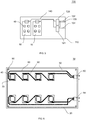
- Fig. 1 shows an LED lighting module 10 according to embodiments in a plan view.
- the printed circuit board also referred to as board below
- eight light-emitting diodes (LEDs) 40 are arranged in two rows of 4 LEDs each.
- the LEDs are slightly larger (their outline lines hidden in the board are in Fig. 1 Dashed lines) as the openings 70 in board 30.
- the terminals of the LEDs 40 are guided to one side of the board, where they are completed with a multi-pin socket 50 which is mounted on the board.
- the interconnects 60 extend in the view of Fig. 1 on the side facing away from the viewer surface of the board 30, on which the LEDs are mounted. Other geometrical arrangements are also possible, as described below.
- the conductor tracks 60 can also run on the other side of the board 30, ie in the Fig. 1 on the side of the board facing the viewer. If the board 30 has several layers, that is a multilayer board, the printed conductors can also run in an intermediate layer of the board. Also mixed forms between the above are possible. Depending on the design, feedthroughs may be provided from the printed conductors through the printed circuit board or part of the printed circuit board to the LEDs.
- the board 30 is, typically at its corners, with post / spacers 80 with the Aluminum plate 20 connected, which serves as a heat sink. The light emission of the LEDs is directed in this representation of the drawing plane to the viewer.
- Fig. 2 shows a schematic side view of the LED lighting module of Fig. 1 , Thermal paste (not shown) provides improved heat transfer between the housings of the LEDs 40 and the aluminum plate 20.
- the holes 70 in the circuit board are shown in phantom.
- the emission direction of the LEDs 40 is shown schematically by arrows in the example of the left of the four illustrated light emitting diodes.
- the emitted light passes through the apertures 70 in the circuit board 30, that is, the light passes through the circuit board 30 through the apertures 70.
- the LEDs are fitted in additional recesses in the circuit board 30 rather than in FIG Fig. 2 shown mounted on the surface, the emitted light traverses only a portion of the thickness of the board, for example, 30%, 50% or 70% of the thickness of the board (not shown).
- the apertures 70 are typically from about 5% to about 30% larger (by diameter) than the effective radiating area of the light emitting diode 40, or a projection of the radiating surface of the light emitting diode onto the plane of the circuit board.
- the dimensions of the openings are to be chosen so that on the one hand, the opening is large enough not to block the radiated light, on the other hand, the opening is smaller than the base of the LED on its emission side, since the LED rests on its edges on the board ,
- an LED lighting module 10 may include from 1 to 64 light emitting diodes 40 and as many holes / openings 70, typically arranged as an mxn matrix, such as (non-limiting) 1 x 1, 1 x 2, 2 x 2, 2 x 3, 2 x 4, 4 x 4, etc.
- the LEDs 40 used have a different shape from that described here of a flat cuboid, this may require changes to the structure described, which represents a standard task for a person skilled in the art.
- a non-planar back side of the LEDs could require corresponding recesses in the heat sink 20 in order to ensure a corresponding surface contact between LED and heat sink, and thus good heat dissipation.
- Fig. 3 shows a lighting fixture 130, in which three LED lighting modules 10 (shown only schematically here) according to embodiments in a lamp housing 110 are installed.
- the three modules 10 are connected via cable 140 to a ballast 120, which is designed to transform the 115 or 230 volt AC mains voltage to the operating voltage of the modules 10, typically from 6 to 120 volts DC, eg 6, 12, 24, 48 , 60 or 96 volts.
- the ballast 120 is designed as a switching power supply.
- the aluminum plates 20 can be connected / bonded in a planar manner to an inner wall of the housing 110 using thermal paste.
- the power supply may additionally be equipped with control functions to enable single switching on / control of individual LEDs or of groups. Any number of lighting modules 10 may be incorporated into a common housing 110 limited only by its dimensions and the performance of the one or more ballasts 120.
- the LED modules 10 may be configured to be connected through the connector 50 also in FIG Position are kept and thus easily replaceable. An additional clamping device or the like may also be provided to ensure thermal contact with the housing 110.
- Fig. 4 is a side cross-sectional view of a similar embodiment as that of Fig. 3 shown.
- Fig. 5 shows a further embodiment, analogous to that of 3 and 4 ,
- two LED lighting modules each with four LEDs 40 are mounted in a housing 110.
- the two modules are each powered by a ballast 120, 121 with DC voltage.
- the two ballasts are connected to a common neutral conductor 132.
- the connections for the mains alternating voltage 133, 134 can, as shown, be designed separately for both ballasts 120, 121. If these are connected to different phases of the supply current network, a simple circuit of the illuminance can be realized in this way.
- the illuminance can be reduced without the need for a separate switching device or electronics in the lamp housing.
- several ballasts per lighting module 10 may be provided.
- Fig. 6 shows an embodiment of an LED lighting module 10 similar to that of Fig. 1 ,
- eight LEDs are combined in two groups of four LEDs connected in series. The connections are led separately to the sockets 50, 51, so that both groups can optionally be switched or controlled separately, analogously to the example in FIG Fig. 5
- ballasts which may optionally be connected to different phases.
- a side view of this embodiment substantially corresponds to the illustration in FIG Fig. 2 ,
- the LEDs 40 and typically the tracks 60 are located in this example on the side facing away from the viewer side of the board 30, but are shown for illustrative purposes. For other possible levels of the conductor tracks the same applies as in Fig. 1 described.
- a combination of two such modules, each with 8 high-power LEDs, each about 6 to 9 W, in a lamp housing is suitable from the achieved luminance, for example as a lighting fixture for street lighting purposes.
- Fig. 7 schematically shows embodiments in which a plurality of LEDs 40 are arranged in a circular or star-shaped arrangement on the first side of the board 30.
- the light-emitting diodes 40 are high-power light-emitting diodes. These are typically cuboid with a low height-to-width ratio, but may be e.g. also have a round or elliptical form factor.
- height refers to the dimension in the main or symmetry direction of the light emission. Preferably, the height is less than 20% of the respective larger of width and length.
- Typical size ranges are 0.5 to 8 mm height (measured without any optical attachment element), more particularly 1 mm to 3 mm, and each (independently of each other) 5 to 120 mm in length and width, more particularly 8 mm to 30 mm.
- An exemplary, non-limiting LED may have dimensions of 12 x 15 x 1.6 mm (L x W x H) and a power consumption of 7 W. Typical power consumption is 1 W to 100 W, more specifically 3 W to 50 W.
- Lighting fixtures according to embodiments using LED modules 10 as described may further include a blower 200. This blows or sucks air in the Gap or air space 205 between board 30 and heat sink 20 to increase the cooling, which in Fig. 8 is shown.
- Lighting fixtures may further comprise a thermosyphone 210 or a heat pipe 220, which is in thermal communication with the backside of the LEDs.
- the heat sink 20 may be arranged as in previous examples, and in addition to the thermosyphone 210 or the heat pipe 220 are in communication, so that the waste heat is transported to a heat sink / condenser 230. This is in Fig. 9 shown schematically. Both elements 210, 220 may be thermally connected directly to the LED backs without heat sink 20.
- the LED modules according to embodiments are suitable as replaceable lighting fixtures as a replacement for conventional illuminants such as halogen bulbs or rods.
- the connection can be made to the power supply via plug, so that the module can be quickly and easily replaced by laymen in case of a defect or to change the illuminance.
- the power connector may be configured to hold the module in position at the same time, such as by combination with the posts / spacers 80.
- the heat sink 20 may be part of the module 10, or part of the lamp 130.
Landscapes
- Engineering & Computer Science (AREA)
- General Engineering & Computer Science (AREA)
- Physics & Mathematics (AREA)
- Microelectronics & Electronic Packaging (AREA)
- Optics & Photonics (AREA)
- Arrangement Of Elements, Cooling, Sealing, Or The Like Of Lighting Devices (AREA)
- Non-Portable Lighting Devices Or Systems Thereof (AREA)
- Fastening Of Light Sources Or Lamp Holders (AREA)
Description
- Ausführungsformen der vorliegenden Erfindung betreffen Beleuchtungsmodule, insbesondere unter Verwendung von Leuchtdioden (LED). Im Speziellen betreffen sie LED-Beleuchtungsmodule mit vereinfachter Herstellung und verbesserter Ableitung der Verlustwärme.
- Durch die Entwicklung von Leuchtdioden (LED) mit weißer Lichtcharakteristik und einer gleichzeitigen stetigen Leistungssteigerung haben sich LEDs in den letzten Jahren zu einer vielversprechenden Alternative zu herkömmlichen Beleuchtungsmitteln sowohl im Privat- und gewerblichen Bereich als auch im öffentlichen Sektor entwickelt. So wird etwa im bisher vor allem von Metalldampflampen (z.B. Natriumdampflampen, Quecksilberdampflampen) dominierten Bereich der Straßenbeleuchtung zunehmend LED-Technologie eingesetzt, die sich in punkto Lebensdauer, Lichtausbeute und unter Kostenaspekten zu einer vorteilhaften Alternative entwickelt hat. Im Gegensatz zu der weitgehend ausentwickelten, herkömmlichen Metalldampftechnik ist die LED-Technik von stetiger Weiterentwicklung geprägt, wodurch in vielen Aspekten weitere signifikante Fortschritte zu erwarten sind. Daher haben bereits deutliche Marktverschiebungen eingesetzt.
- So verglich eine Studie der Universität Pittsburgh 2009 die Straßenbeleuchtung mit LEDs mit der mit Natriumdampf-Hochdrucklampen sowie mit Halogen-Metalldampflampen (Hartley et al.: "Life Cycle Assessment of Streetlight Technologies", Universität Pittsburgh, Juli 2009) Das Ergebnis der Studie war, dass die LED-Beleuchtung schon 2009 einen ähnlichen Ressourcenverbrauch über die Lebensdauer erzeugte wie die anderen Technologien, wobei den LEDs aber noch großes Potential zur Optimierung bescheinigt wurde. Daher empfahlen die Autoren mittelfristig einen kompletten Umstieg auf LEDs zur Straßenbeleuchtung. Seit der Studie hat sich die LED-Technologie in Bezug auf Lichtausbeute und Energieeffizienz signifikant weiterentwickelt, so dass die damals prognostizierten Vorteile bereits Realität sind.
- Durch die stetige Erhöhung der Leuchtdichten hat sich gleichzeitig ein Aspekt relativiert, der früher LEDs als "kalte" Alternative zu herkömmlichen Glüh- oder Entladungslampen auszeichnete. So sind bei marktüblichen weißen Hochleistungs-LEDs Verlustleistungen bis über 10 Watt bei äußeren Abmessungen (Grundfläche) von weniger als etwa 1 cm2 üblich. Da sowohl Wirkungsgrad bzw. Leistungsausbeute, als auch die Lebensdauer bei steigender Temperatur des Halbleiter-Substrats negativ beeinflusst werden, ist es daher eine zunehmende Herausforderung, die auftretenden Verlustleistungen schnell und zuverlässig abzuleiten. Üblicherweise sind zur Erzielung ausreichender Beleuchtungsstärken mehrere einzelne LEDs zu einem Beleuchtungsmodul zusammengefasst, das heißt in der Praxis matrixartig auf einer gemeinsamen Basis wie einer Leiterplatte angebracht. Hochleistungs-LEDs haben üblicherweise annähernd die Form einer flachen Scheibe bzw. eines sehr flachen Quaders. Sie sind typischerweise wie herkömmliche Elektronik-Bauelemente auf der Bestückungsseite der Leiterplatte angebracht und kontaktiert. Weil das Glasfaser-Epoxid-Verbundmaterial üblicher Leiterplatten im Vergleich zu Metallen wie Kupfer oder Aluminium ein schlechter Wärmeleiter ist, wurden verschiedene Techniken zur Verbesserung der Wärmeabfuhr entwickelt.
- Dazu gehört etwa ein Verbundwerkstoff aus einer Schicht Leiterplattenmaterial (PCB) mit einer direkt darunter liegenden Aluminiumplatte. Die LEDs sind dabei auf dem PCB-Material aufgebracht und kontaktiert, wobei die Aluminiumplatte die Aufgabe der Wärmeableitung bzw. des Kühlkörpers übernimmt. Diese und ähnliche Lösungen haben jedoch mehrere Nachteile. Zum einen sind solche Verbundleiterplatten wegen der geringeren Stückzahlen und ihrem komplexeren Aufbau teurer als herkömmliche Leiterplatten, zum anderen stellt das Leiterplattenmaterial, bzw. gegebenenfalls auch weitere Isolierungsschichten, eine unerwünschte thermische Barriere zwischen der LED und der Aluminiumplatte dar.
- Zur Lösung dieses Problems wurden zur Verbesserung des Wärmeübergangs Zusatztechniken eingeführt. So werden z.B. metallische Durchführungen durch die Leiterplatte eingesetzt, um einen besseren thermischen Kontakt zwischen der LED-Rückseite und der Aluminiumplatte herstellen. Diese Durchführungen durch die Leiterplatte bzw. verwandte Lösungen erhöhen jedoch die Fertigungskomplexität, die Anzahl der Fertigungsschritte und die Kosten. Zudem sind solche Durchführungen typischerweise nur unter einem Teil der Querschnittsfläche des LED-Gehäuses realisiert (vgl. etwa: Osram Opto Semiconductors: "Thermal Management of Golden Dragon LED", Application Note, Oktober 2008).
- Die
US 2009 / 0068856 A1 offenbart ein LED-Beleuchtungsmodul mit einer Leiterplatte mit einer Mehrzahl von Löchern. In den Löchern sind LED-Chips auf Metallplatten angebracht. DieEP 1696404 A1 offenbart eine Anordnung mit einer Leuchtdiode. Eine emittierende Oberfläche der Diode ist in Richtung der Leiterplatte gerichtet, die in einer Strahlungsrichtung der Leuchtdiode bereichsweise durchscheinend ist. - Im Hinblick auf die angeführten Probleme ist es eine Aufgabe der vorliegenden Erfindung, ein LED-Beleuchtungsmodul bereitzustellen, das die Nachteile der bekannten Lösungen vermeidet.
- Diese Aufgabe wird, zumindest teilweise, von einem LED-Beleuchtungsmodul gemäß Anspruch 1 gelöst.
- Gemäß einem ersten Aspekt wird ein LED-Beleuchtungsmodul bereitgestellt. Das LED-Beleuchtungsmodul umfasst eine Platine, mit einer ersten und einer zweiten Seite und mindestens einer durchgehenden Öffnung, mindestens eine an der Öffnung, auf der ersten Seite der Platine angebrachte Leuchtdiode mit einer licht-emittierenden Vorderseite und einer nicht-emittierenden Rückseite, einen Kühlkörper an der nicht-emittierenden Rückseite der mindestens einen Leuchtdiode, dadurch gekennzeichnet, dass die mindestens eine Leuchtdiode eine Leistungsaufnahme von 1 bis 100 W hat, und mit ihrer licht-emittierenden Vorderseite an der ersten Seite der Platine so angebracht ist, dass die mindestens eine Leuchtdiode an ihren Rändern auf der Platine aufliegt, und dass emittiertes Licht durch die mindestens eine Öffnung in der Platine hindurchtritt und dabei die Platine durch die Öffnung durchquert, wobei der Abstand zwischen der Platine und dem Kühlkörper der Ausdehnung der Leuchtdiode in der Richtung ihrer Lichtemission entspricht.
- Weitere Vorteile, Merkmale, Aspekte und Details der Erfindung sowie bevorzugte Ausführungen und besondere Aspekte der Erfindung ergeben sich aus den Ansprüchen, der Beschreibung und den Figuren.
- Im Weiteren soll die Erfindung anhand von in Figuren dargestellten Ausführungsbeispielen erläutert werden, aus denen sich weitere Vorteilteile und Abwandlungen ergeben. Dabei zeigen:
-
Fig. 1 zeigt eine Draufsicht auf ein LED-Beleuchtungsmodul gemäß Ausführungsbeispielen. -
Fig. 2 zeigt eine Seitenansicht des LED-Beleuchtungsmoduls derFig. 1 . -
Fig. 3 zeigt eine schematische Querschnittsansicht durch eine Lampe mit LED-Beleuchtungsmodulen gemäß Ausführungsbeispielen. -
Fig. 4 zeigt eine seitliche schematische Querschnittsansicht durch eine Lampe mit LED-Beleuchtungsmodulen gemäß Ausführungsbeispielen. -
Fig. 5 zeigt eine schematische Querschnittsansicht einer Lampe mit LED-Beleuchtungsmodulen gemäß Ausführungsbeispielen. -
Fig. 6 zeigt eine Draufsicht auf ein LED-Beleuchtungsmodul gemäß weiteren Ausführungsbeispielen. -
Fig. 7 zeigt eine schematische Draufsicht auf ein LED-Beleuchtungsmodul gemäß Ausführungsbeispielen. -
Fig. 8 zeigt eine Querschnittsansicht durch ein LED-Beleuchtungsmodul gemäß Ausführungsbeispielen. -
Fig. 9 zeigt eine Querschnittsansicht durch ein LED-Beleuchtungsmodul gemäß weiteren Ausführungsbeispielen. - Im Folgenden wird beispielhaft von üblichen Hochleistungs-LEDs ausgegangen, die jeweils etwa 1 cm lang, 1 cm breit und etwa 2 mm hoch sind. Dies ist jedoch nur als nichtlimitierendes Beispiel zu sehen, Ausführungsformen der Erfindung beziehen sich auch auf anders geformte Leuchtdioden mit anderen Abmaßen. Ferner werden die Begriffe LED und Leuchtdiode hier synonym verwendet.
- Ausführungsformen betreffen eine Leiterplatte bzw. Platine, die mit mehreren durchgehenden Öffnungen versehen ist. Die Öffnungen haben typischerweise jeweils etwa die gleiche Form wie die effektive Abstrahlfläche einer einzelnen LED, sind aber größer, z.B. jeweils um etwa 5 % bis etwa 30 % in Länge und Breite. Zum Beispiel können die Öffnungen 70 die gleiche Form wie die effektive Abstrahlfläche der LED haben, aber im Durchmesser 1 mm oder 2 mm größer sein als diese. Die Form der Öffnungen 70 kann auch der Form der Fläche der Abstrahlseite der LEDs entsprechen, aber etwa 1 bis 3 mm kleiner als diese sein. Die LEDs sind auf der Leiterplatte so angebracht, dass ihre lichtemittierende Seite der Leiterplatte zugewandt ist, bzw. an einer ersten Seite der Leiterplatte oder Platine angebracht ist, dass also das im Betrieb emittierte Licht durch die Öffnungen der Leiterplatte strahlt und auf einer zweiten Seite der Leiterplatte/Platine austritt. Die üblicherweise plane (nicht lichtemittierende) Rückseite der LEDs ist dementsprechend gegenüber der Fläche der Leiterplatte erhaben angeordnet, wobei die einzelnen Rückseiten der LEDs typischerweise auf einer gemeinsamen Ebene liegen. Die Kontaktierung der einzelnen LEDs zur Leiterplatte kann dabei auf verschiedene, dem Fachmann bekannte Verfahren bereitgestellt sein.
- An den gemeinsam eine Ebene bildenden Rückseiten der LEDs ist eine Metallplatte angebracht, typischerweise aus Aluminium oder einem anderen gut wärmeleitenden Material wie etwa Kupfer. Dabei kann zwischen den LED-Rückseiten und der Metallplatte ein dünn (typischerweise weniger als 0,5 mm) aufgebrachtes Mittel zur Verbesserung des Wärmeübergangs vorgesehen sein, typischerweise Wärmeleitpaste.
- Im Betrieb emittieren die LEDs Licht durch die Löcher der Leiterplatte. Durch die vergleichsweise geringe Dicke der Leiterplatte im Vergleich zur Größe der Öffnungen bzw. durch entsprechende Abstimmung zwischen Abstrahlcharakteristik der LED und der Öffnungsgröße kann eine Verringerung des Abstrahlwinkels verhindert bzw. minimiert werden. Die Verlustwärme der LEDs wird jeweils über ihre gesamte (typischerweise plane) Rückseite in die Metallplatte bzw. den Kühlkörper geleitet, wodurch eine hocheffiziente Kühlung erzielt wird. Die Metallplatte sollte eine ausreichende Dicke haben, typischerweise mindestens etwa 2 mm, damit ein ausreichender Abtransport der Verlustwärme aus dem Kontaktbereich mit der LED gewährleistet ist. Wäre die Metallplatte dagegen nicht ausreichend dick bzw. aus nicht ausreichend wärmeleitfähigem Material, könnte der Abtransport der Wärmeenergie aus der Kontaktzone mit der LED nicht ausreichend sein. Die Dicke der Platte kann in Ausführungsbeispielen von 2 mm bis 10 mm betragen, insbesondere von 3 mm bis 7 mm.
- Die entsprechende Wahl des Materials für die Metallplatte sowie deren geometrische Auslegung sind in Abhängigkeit von der Verlustleistung der einzelnen LEDs und deren Anzahl pro Leiter- bzw. Metallplatte festzulegen. Die Durchführung entsprechender Auslegungsversuche und -berechnungen bzw. thermischer Simulationen gehört zum Standardwissen des Fachmanns.
-
Fig. 1 zeigt ein LED-Beleuchtungsmodul 10 gemäß Ausführungsformen in einer Draufsicht. Zwischen der Aluminiumplatte 20 und der Leiterplatte (im Folgenden auch Platine genannt) 30 sind acht Leuchtdioden (LEDs) 40 in zwei Reihen zu je 4 LEDs angeordnet. Die LEDs sind etwas größer (ihre von der Platine verdeckten Umrisslinien sind inFig. 1 gestrichelt dargestellt) als die Öffnungen 70 in Platine 30. Über in der Platine angeordnete Leiterbahnen 60 sind die Anschlüsse der LEDs 40 an eine Seite der Platine geführt, wo sie mit einer Mehrpol-Buchse 50 abgeschlossen sind, die auf der Platine befestigt ist. Die Leiterbahnen 60 verlaufen in der Ansicht derFig. 1 auf der vom Betrachter abgewandten Fläche der Platine 30, auf der auch die LEDs angebracht sind. Es sind auch andere geometrische Anordnungen möglich, wie im weiteren noch beschrieben. - In Ausführungsbeispielen können die Leiterbahnen 60 auch auf der anderen Seite der Platine 30 verlaufen, d.h. in der
Fig. 1 auf der dem Betrachter zugewandten Seite der Platine. Wenn die Platine 30 mehrere Schichten hat, also eine Multilayerplatine ist, können die Leiterbahnen auch in einer Zwischenschicht der Platine verlaufen. Auch Mischformen zwischen den vorgenannten sind möglich. Je nach Ausführung können dabei Durchführungen von den Leiterbahnen durch die Platine oder einen Teil der Platine zu den LEDs vorgesehen sein. Die Platine 30 ist, typischerweise an ihren Ecken, mit Pfosten/Distanzstücken 80 mit der Aluminiumplatte 20 verbunden, die als Kühlkörper dient. Die Lichtabstrahlung der LEDs ist in dieser Darstellung von der Zeichenebene auf den Betrachter gerichtet. -
Fig. 2 zeigt eine schematische Seitenansicht des LED-Beleuchtungsmoduls derFig. 1 . Wärmeleitpaste (nicht dargestellt) sorgt für einen verbesserten Wärmeübergang zwischen den Gehäusen der LEDs 40 und der Aluminiumplatte 20. Die Löcher bzw. Öffnungen 70 in der Platine sind gestrichelt dargestellt. Die Abstrahlrichtung der LEDs 40 ist exemplarisch bei der linken der vier dargestellten Leuchtdioden schematisch durch Pfeile dargestellt. Das emittierte Licht tritt durch die Öffnungen 70 in der Platine 30 hindurch, das heißt das Licht durchquert die Platine 30 durch die Öffnungen 70. In anderen Ausführungsformen, in denen etwa die LEDs in zusätzliche Vertiefungen in der Platine 30 eingepasst sind und nicht wie inFig. 2 gezeigt auf deren Oberfläche angebracht sind, durchquert das emittierte Licht nur einen Teil der Dicke der Platine, z.B. 30 %, 50 % oder 70% der Dicke der Platine (nicht dargestellt). - In Ausführungsformen sind die Öffnungen 70 typischerweise von etwa 5 % bis etwa 30 % größer (auf den Durchmesser bezogen) als die effektive Abstrahlfläche der Leuchtdiode 40, bzw. einer Projektion der Abstrahlfläche der Leuchtdiode auf die Ebene der Platine. Die Abmessungen der Öffnungen sind so zu wählen, dass einerseits die Öffnung groß genug ist, um das abgestrahlte Licht nicht zu blockieren, andererseits die Öffnung kleiner ist als die Grundfläche der LED auf ihrer Abstrahlseite, da die LED ja an ihren Rändern auf der Platine aufliegt.
- In Ausführungsformen kann ein LED-Beleuchtungsmodul 10 von 1 bis 64 Leuchtdioden 40 und ebenso viele Löcher/Öffnungen 70 umfassen, die typischerweise als m x n Matrix angeordnet sind, etwa (nicht-limitierend) 1 x 1, 1 x 2, 2 x 2, 2 x 3, 2 x 4, 4 x 4, etc.
- Haben die verwendeten LEDs 40 eine andere Form als die hier beschriebene eines flachen Quaders, kann dies Änderungen des beschriebenen Aufbaus erfordern, was eine Standardaufgabe für einen Fachmann darstellt. So könnte eine nicht-plane Rückseite der LEDs entsprechende Aussparungen/Ausfräsungen in dem Kühlkörper 20 erfordern, um einen entsprechenden flächigen Kontakt zwischen LED und Kühlkörper, und damit eine gute Wärmeabführung, sicherzustellen.
-
Fig. 3 zeigt einen Beleuchtungskörper 130, bei dem drei LED-Beleuchtungsmodule 10 (hier nur schematisch dargestellt) gemäß Ausführungsformen in ein Lampengehäuse 110 eingebaut sind. Die drei Module 10 sind über Kabel 140 mit einem Vorschaltgerät 120 verbunden, dass zur Transformierung der 115 oder 230 Volt Netz-Wechselspannung auf die Betriebsspannung der Module 10 ausgelegt ist, typischerweise von 6 bis 120 Volt Gleichspannung, z.B. 6, 12, 24, 48, 60 oder 96 Volt. Typischerweise ist das Vorschaltgerät 120 als Schaltnetzteil ausgelegt. Um eine gute Wärmeabfuhr von den LED-Modulen 10 an die Umgebung der Lampe 130 zu gewährleisten, können die Aluminiumplatten 20 unter Verwendung von Wärmeleitpaste flächig mit einer Innenwand des Gehäuses 110 verbunden/verschraubt sein. Das Netzteil kann zusätzlich mit Steuerfunktionen ausgerüstet sein, um ein einzelnes Einschalten/Steuern einzelner LEDs oder von Gruppen zu ermöglichen. Es kann eine beliebige Anzahl von Beleuchtungsmodulen 10 in ein gemeinsames Gehäuse 110 eingebaut sein, begrenzt nur durch dessen Abmessungen und die Leistungsfähigkeit des einen oder der mehreren Vorschaltgeräte 120. Die LED-Module 10 können so ausgeführt sein, dass sie durch die Steckverbindung 50 auch in Position gehalten werden und somit leicht austauschbar sind. Es kann auch eine zusätzliche Klemmvorrichtung oder ähnliches vorgesehen sein, um den thermischen Kontakt zum Gehäuse 110 zu sichern. - In der
Fig. 4 ist eine seitliche Querschnittsansicht eines ähnlichen Ausführungsbeispiels wie das derFig. 3 gezeigt. -
Fig. 5 zeigt eine weitere Ausführungsform, analog zu der derFig. 3 und 4 . Dabei sind zwei LED-Beleuchtungsmodule mit je vier LEDs 40 in einem Gehäuse 110 montiert. Die zwei Module werden von je einem Vorschaltgerät 120, 121 mit Gleichspannung versorgt. Die zwei Vorschaltgeräte sind an einen gemeinsamen Nulleiter 132 angeschlossen. Die Anschlüsse für die Netzwechselspannung 133, 134 können, wie dargestellt, für beide Vorschaltgeräte 120, 121 getrennt ausgeführt sein. Wenn diese an verschiedene Phasen des Speisestromnetzes angeschlossen sind, kann auf diese Weise eine einfache Schaltung der Beleuchtungsstärke realisiert werden. Durch Abschalten einer der beiden (in anderen Ausführungsformen einer oder zwei von drei) Phasen lässt sich so die Beleuchtungsstärke reduzieren, ohne dass dazu eine eigene Schaltvorrichtung bzw. Elektronik im Lampengehäuse erforderlich ist. In weiteren Ausführungsbeispielen, siehe etwaFig. 6 unten, können auch mehrere Vorschaltgeräte pro Beleuchtungsmodul 10 vorgesehen sein. -
Fig. 6 zeigt ein Ausführungsbeispiel eines LED-Beleuchtungsmoduls 10 ähnlich dem derFig. 1 . Dabei sind acht LEDs in zwei Gruppen zu je vier in Reihe geschalteten LEDs zusammengefasst. Die Anschlüsse sind separat an die Buchsen 50, 51 geführt, so dass beide Gruppen gegebenenfalls separat geschaltet bzw. gesteuert werden können, analog zu dem Beispiel inFig. 5 z.B. mit verschiedenen Vorschaltgeräten, die gegebenenfalls an unterschiedliche Phasen angeschlossen sein können. Eine Seitenansicht dieses Ausführungsbeispiels entspricht im Wesentlichen der Darstellung inFig. 2 . Die LEDs 40 sowie typischerweise die Leiterbahnen 60 befinden sich in diesem Beispiel auf der vom Betrachter abgewandten Seite der Platine 30, sind aber aus Darstellungsgründen eingezeichnet. Zu anderen möglichen Verlaufsebenen der Leiterbahnen gilt das Gleiche wie beiFig. 1 beschrieben. Eine Kombination zweier derartiger Module, mit je 8 Hochleistungs-LEDs zu je etwa 6 bis 9 W, in einem Lampengehäuse eignet sich von der erzielten Leuchtdichte zum Beispiel als Beleuchtungskörper für Zwecke der Straßenbeleuchtung. -
Fig. 7 zeigt schematisch Ausführungsformen, bei denen mehrere Leuchtdioden 40 in einer kreisförmigen oder sternförmigen Anordnung an der ersten Seite der Platine 30 angeordnet sind. Dadurch können etwa eventuell vorhandene gerichtete Abstrahlcharakteristiken der LEDs teilweise ausgeglichen werden, wodurch die Gleichmäßigkeit der Winkelverteilung der Lichtabgabe steigt. - In Ausführungsbeispielen sind die Leuchtdioden 40 Hochleistungsleuchtdioden. Diese sind typischerweise quaderförmig mit einem niedrigen Höhe-zu-Breite-Verhältnis, können aber z.B. auch einen runden oder elliptischen Formfaktor haben. Hierbei bezieht sich Höhe auf die Dimension in Haupt- bzw. Symmetrierichtung der Lichtemission. Bevorzugt beträgt die Höhe weniger als 20 % der jeweils größeren von Breite und Länge. Typische Größenbereiche sind 0,5 bis 8 mm Höhe (ohne ein eventuell vorhandenes optisches Vorsatzelement gemessen), spezieller 1 mm bis 3 mm, und jeweils (unabhängig voneinander) 5 bis 120 mm Länge und Breite, spezieller 8 mm bis 30 mm. Eine beispielhafte, nicht-limitierende LED kann etwa Abmessungen von 12 x 15 x 1,6 mm (L x B x H) haben und eine Leistungsaufnahme von 7 W. Typische Leistungsaufnahmen sind 1 W bis 100 W, spezieller 3 W bis 50 W.
- Beleuchtungskörper gemäß Ausführungsbeispielen, die LED-Module 10 wie beschrieben verwenden, können ferner ein Gebläse 200 umfassen. Dieses bläst oder saugt Luft in den Spalt bzw. Luftraum 205 zwischen Platine 30 und Kühlkörper 20 zur Erhöhung der Kühlung, was in
Fig. 8 dargestellt ist. - Beleuchtungskörper gemäß Ausführungsbeispielen können ferner einen Thermosyphon 210 oder eine Heatpipe 220 umfassen, welches mit der Rückseite der LEDs in thermischer Verbindung steht. Hierzu kann der Kühlkörper 20 wie in vorigen Beispielen angeordnet sein, und zusätzlich mit dem Thermosyphon 210 oder der Heatpipe 220 in Verbindung stehen, so dass die Abwärme zu einem Kühlkörper/Kondensor 230 transportiert wird. Dies ist in
Fig. 9 schematisch dargestellt. Beide Elemente 210, 220 können auch ohne Kühlkörper 20 direkt mit den LED-Rückseiten thermisch verbunden sein. - Die LED-Module gemäß Ausführungsformen eignen sich als wechselbare Beleuchtungskörper als Ersatz für herkömmliche Leuchmittel wie Halogenbirnen oder -stäbe. Dazu kann die Verbindung zur Stromversorgung über Stecker geschehen, so dass das Modul bei einem Defekt oder zum Wechseln der Beleuchtungsstärke schnell und einfach auch von Laien getauscht werden kann. Zudem kann die Strom-Steckverbindung so gestaltet sein, dass sie das Modul gleichzeitig in Position hält, etwa durch Kombination mit den Pfosten/Distanzstücken 80. Dabei kann in Ausführungsbeispielen der Kühlkörper 20 Teil des Moduls 10 sein, oder Teil der Leuchte 130.
- Die in der vorstehenden Beschreibung, in den Ansprüchen sowie in den Zeichnungen offenbarten Merkmale der Erfindung können sowohl einzeln als auch in jeder beliebigen, technisch sinnvollen Kombination für die Verwirklichung der Erfindung in ihren verschiedenen Ausführungsformen wesentlich sein.
Claims (13)
- LED-Beleuchtungsmodul (10), umfassend:eine Platine (30), mit einer ersten und einer zweiten Seite und mindestens einer durchgehenden Öffnung (70),mindestens eine an der Öffnung (70), auf der ersten Seite der Platine (30) angebrachte Leuchtdiode (40) mit einer licht-emittierenden Vorderseite und einer nicht-emittierenden Rückseite,einen Kühlkörper (20) an der nicht-emittierenden Rückseite der mindestens einen Leuchtdiode (40),dadurch gekennzeichnet,dass die mindestens eine Leuchtdiode (40) eine Leistungsaufnahme von 1 bis 100 W hat, undmit ihrer licht-emittierenden Vorderseite an der ersten Seite der Platine so angebracht ist, dass die mindestens eine Leuchtdiode (40) an ihren Rändern auf der Platine (30) aufliegt, und dass emittiertes Licht durch die mindestens eine Öffnung (70) in der Platine (30) hindurchtritt und dabei die Platine (30) durch die Öffnung (70) durchquert,wobei der Abstand zwischen der Platine (30) und dem Kühlkörper (20) der Ausdehnung der Leuchtdiode (40) in der Richtung ihrer Lichtemission entspricht.
- LED-Beleuchtungsmodul (10) nach Anspruch 1, wobei die Platine (30) Leiterbahnen (60) umfasst, und wobei die Kontaktierung der Leuchtdiode (40) zu einer Leiterbahn (60) auf der Seite der Platine (30) angeordnet ist, welche der Richtung der Lichtemission entgegengesetzt ist.
- LED-Beleuchtungsmodul (10) nach Anspruch 1 oder 2, wobei die Öffnung (70) kleiner als eine Grundfläche der Leuchtdiode (40) ist.
- LED-Beleuchtungsmodul (10) nach einem der vorhergehenden Ansprüche, wobei die Öffnung (70) 5 % bis 30 % größer als die effektive emittierende Fläche der Leuchtdiode ist.
- LED-Beleuchtungsmodul (10) nach einem der vorhergehenden Ansprüche, umfassend 1 bis 64 Leuchtdioden (40) und 1 bis 64 Öffnungen (70) für die Leuchtdioden.
- LED-Beleuchtungsmodul (10) nach einem der vorhergehenden Ansprüche, wobei der Kühlkörper (20) eine Metallplatte ist.
- LED-Beleuchtungsmodul (10) nach einem der vorhergehenden Ansprüche, wobei zwischen Kühlkörper (20) und der ersten Seite der Platine (30) ein Luftvolumen (205) besteht.
- LED-Beleuchtungsmodul nach einem der vorhergehenden Ansprüche, wobei mehrere Leuchtdioden (40) in einer m x n Matrix an der ersten Seite der Platine (30) angeordnet sind.
- LED-Beleuchtungsmodul nach einem der Ansprüche 1 bis 8, wobei mehrere Leuchtdioden (40) in einer kreisförmigen oder sternförmigen Anordnung an der ersten Seite der Platine (30) angeordnet sind.
- LED-Beleuchtungsmodul nach einem der vorhergehenden Ansprüche, wobei die Leuchtdioden quaderförmige Hochleistungsleuchtdioden mit einem niedrigen Höhe-zu-Breite-Verhältnis sind, bevorzugt beträgt die Höhe gleich oder weniger als 20 % der jeweils größeren von Breite und Länge.
- Beleuchtungskörper mit einem LED-Beleuchtungsmodul (10) gemäß einem der Ansprüche 1 bis 10.
- Beleuchtungskörper nach Anspruch 11, ferner umfassend ein Gebläse (200), wobei zwischen Platine (30) und dem Kühlkörper (20) ein Luftvolumen (205) vorhanden ist, in den mittels des Gebläses (200) Kühlluft geblasen wird.
- Beleuchtungskörper nach Anspruch 11 oder 12, ferner umfassend mindestens eines der Elemente aus der Liste: ein Thermosyphon (210), und eine Heatpipe (220), welches mit der Rückseite der LEDs (40) in thermischer Verbindung steht.
Applications Claiming Priority (1)
| Application Number | Priority Date | Filing Date | Title |
|---|---|---|---|
| DE202011050596U DE202011050596U1 (de) | 2011-06-30 | 2011-06-30 | LED-Beleuchtungsmodul |
Publications (3)
| Publication Number | Publication Date |
|---|---|
| EP2541139A2 EP2541139A2 (de) | 2013-01-02 |
| EP2541139A3 EP2541139A3 (de) | 2013-08-07 |
| EP2541139B1 true EP2541139B1 (de) | 2017-03-08 |
Family
ID=46514103
Family Applications (1)
| Application Number | Title | Priority Date | Filing Date |
|---|---|---|---|
| EP12174633.3A Not-in-force EP2541139B1 (de) | 2011-06-30 | 2012-07-02 | LED-Beleuchtungsmodul |
Country Status (2)
| Country | Link |
|---|---|
| EP (1) | EP2541139B1 (de) |
| DE (1) | DE202011050596U1 (de) |
Families Citing this family (6)
| Publication number | Priority date | Publication date | Assignee | Title |
|---|---|---|---|---|
| DE102014204757A1 (de) * | 2014-03-14 | 2015-09-17 | Continental Automotive Gmbh | Lichtmodul für einen Kraftfahrzeugscheinwerfer |
| US20170191301A1 (en) | 2014-06-16 | 2017-07-06 | Novoferm Tormatic Gmbh | Drive device for a door |
| SG11201604162YA (en) | 2014-06-16 | 2016-07-28 | Novoferm Tormatic Gmbh | Enclosure for a drive unit of a garage door drive |
| DE102015004080A1 (de) | 2015-03-31 | 2016-10-06 | Novoferm Tormatic Gmbh | llluminationseinheit |
| DE102015002099A1 (de) | 2015-02-23 | 2016-08-25 | Jenoptik Polymer Systems Gmbh | Leuchtdiodenvorrichtung und Verfahren zum Herstellen einer Leuchtdiodenvorrichtung |
| DE202015105853U1 (de) * | 2015-11-04 | 2017-02-08 | Zumtobel Lighting Gmbh | Leuchtvorrichtung |
Family Cites Families (6)
| Publication number | Priority date | Publication date | Assignee | Title |
|---|---|---|---|---|
| US6657767B2 (en) * | 2001-05-21 | 2003-12-02 | Gentex Corporation | Rearview mirror assembly construction |
| EP1696404A1 (de) * | 2005-02-25 | 2006-08-30 | Electrovac, Fabrikation elektrotechnischer Spezialartikel Gesellschaft m.b.H. | Leuchtdiodenanordnung |
| TWM278828U (en) * | 2005-05-11 | 2005-10-21 | Shiu Yung Yuan | LED planar light source module |
| TWI356486B (en) * | 2007-09-07 | 2012-01-11 | Young Lighting Technology | Led light source module and manufacturing method t |
| JP2009117661A (ja) * | 2007-11-07 | 2009-05-28 | Tokai Rika Co Ltd | プリント配線板 |
| DE202008002873U1 (de) * | 2008-02-29 | 2008-05-15 | Martin, Andreas, Dipl.-Ing. | Lichtmodul für Raum- und Flächenausleuchtung |
-
2011
- 2011-06-30 DE DE202011050596U patent/DE202011050596U1/de not_active Expired - Lifetime
-
2012
- 2012-07-02 EP EP12174633.3A patent/EP2541139B1/de not_active Not-in-force
Also Published As
| Publication number | Publication date |
|---|---|
| EP2541139A3 (de) | 2013-08-07 |
| DE202011050596U1 (de) | 2012-08-01 |
| EP2541139A2 (de) | 2013-01-02 |
Similar Documents
| Publication | Publication Date | Title |
|---|---|---|
| EP2541139B1 (de) | LED-Beleuchtungsmodul | |
| DE202010001128U1 (de) | LED-Leuchtvorrichtung mit größerem Leuchtwinkel | |
| WO2009021695A1 (de) | Led-lampe | |
| WO2010136333A1 (de) | Leuchtmodul und leuchtvorrichtung | |
| DE102008016458A1 (de) | Leiterplatte | |
| WO2010108800A1 (de) | Träger mit mindestens einer halbleiterleuchtvorrichtung und trägersystem | |
| DE202010001127U1 (de) | LED-Leuchtvorrichtung mit zwei Leuchtseiten | |
| EP2510276A1 (de) | Halbleiterlampe | |
| DE102014118238A1 (de) | Licht emittierende Vorrichtung, dieselbe beinhaltende Beleuchtungsvorrichtung und Montiersubstrat | |
| DE112011106000T5 (de) | Thermomanagement für Leuchtdioden | |
| WO2009033641A1 (de) | Lampe | |
| WO2016005069A1 (de) | Halbleiterlampe | |
| DE102010003680A1 (de) | Halbleiterlampe | |
| DE112011102961T5 (de) | Hochintensitätslichtquelle | |
| DE102011076128A1 (de) | Trägersystem und Lichtmodul zur Befestigung daran | |
| EP2697557B1 (de) | Beleuchtungseinrichtung | |
| EP2273185A1 (de) | LED-Leuchteneinsatz mit Lichtlenkelement | |
| EP2287519A2 (de) | LED-Modul, Verfahren zu dessen Herstellung und LED-Beleuchtungs-Vorrichtung | |
| EP2307789A1 (de) | Leuchtmittel mit led | |
| DE102010034664B4 (de) | Lichtquelle | |
| WO2010133631A1 (de) | Kühlkörper für eine leuchtvorrichtung | |
| DE102015118984A1 (de) | Lichtquelle | |
| WO2010115395A1 (de) | Leuchtaggregat | |
| AT509626A1 (de) | Modulares led beleuchtungssystem mit partieller lichtstärkenanpassung | |
| DE102009056904B4 (de) | LED-Leuchte |
Legal Events
| Date | Code | Title | Description |
|---|---|---|---|
| PUAI | Public reference made under article 153(3) epc to a published international application that has entered the european phase |
Free format text: ORIGINAL CODE: 0009012 |
|
| AK | Designated contracting states |
Kind code of ref document: A2 Designated state(s): AL AT BE BG CH CY CZ DE DK EE ES FI FR GB GR HR HU IE IS IT LI LT LU LV MC MK MT NL NO PL PT RO RS SE SI SK SM TR |
|
| AX | Request for extension of the european patent |
Extension state: BA ME |
|
| PUAL | Search report despatched |
Free format text: ORIGINAL CODE: 0009013 |
|
| AK | Designated contracting states |
Kind code of ref document: A3 Designated state(s): AL AT BE BG CH CY CZ DE DK EE ES FI FR GB GR HR HU IE IS IT LI LT LU LV MC MK MT NL NO PL PT RO RS SE SI SK SM TR |
|
| AX | Request for extension of the european patent |
Extension state: BA ME |
|
| RIC1 | Information provided on ipc code assigned before grant |
Ipc: F21V 29/00 20060101AFI20130628BHEP Ipc: F21Y 101/02 20060101ALN20130628BHEP Ipc: F21S 2/00 20060101ALN20130628BHEP Ipc: F21W 131/103 20060101ALN20130628BHEP Ipc: F21K 99/00 20100101ALI20130628BHEP Ipc: F21Y 105/00 20060101ALN20130628BHEP |
|
| 17P | Request for examination filed |
Effective date: 20140207 |
|
| 17Q | First examination report despatched |
Effective date: 20150220 |
|
| GRAP | Despatch of communication of intention to grant a patent |
Free format text: ORIGINAL CODE: EPIDOSNIGR1 |
|
| RIC1 | Information provided on ipc code assigned before grant |
Ipc: F21S 2/00 20160101ALN20160829BHEP Ipc: F21V 29/89 20150101ALI20160829BHEP Ipc: F21Y 115/10 20160101ALN20160829BHEP Ipc: F21K 9/00 20160101ALI20160829BHEP Ipc: F21W 131/103 20060101ALN20160829BHEP Ipc: F21V 29/00 20150101AFI20160829BHEP Ipc: F21Y 105/10 20160101ALN20160829BHEP |
|
| INTG | Intention to grant announced |
Effective date: 20160922 |
|
| GRAS | Grant fee paid |
Free format text: ORIGINAL CODE: EPIDOSNIGR3 |
|
| GRAA | (expected) grant |
Free format text: ORIGINAL CODE: 0009210 |
|
| AK | Designated contracting states |
Kind code of ref document: B1 Designated state(s): AL AT BE BG CH CY CZ DE DK EE ES FI FR GB GR HR HU IE IS IT LI LT LU LV MC MK MT NL NO PL PT RO RS SE SI SK SM TR |
|
| REG | Reference to a national code |
Ref country code: GB Ref legal event code: FG4D Free format text: NOT ENGLISH |
|
| REG | Reference to a national code |
Ref country code: CH Ref legal event code: EP Ref country code: AT Ref legal event code: REF Ref document number: 873861 Country of ref document: AT Kind code of ref document: T Effective date: 20170315 |
|
| REG | Reference to a national code |
Ref country code: IE Ref legal event code: FG4D Free format text: LANGUAGE OF EP DOCUMENT: GERMAN |
|
| REG | Reference to a national code |
Ref country code: DE Ref legal event code: R096 Ref document number: 502012009706 Country of ref document: DE |
|
| REG | Reference to a national code |
Ref country code: LT Ref legal event code: MG4D |
|
| REG | Reference to a national code |
Ref country code: NL Ref legal event code: MP Effective date: 20170308 |
|
| REG | Reference to a national code |
Ref country code: FR Ref legal event code: PLFP Year of fee payment: 6 |
|
| PG25 | Lapsed in a contracting state [announced via postgrant information from national office to epo] |
Ref country code: NO Free format text: LAPSE BECAUSE OF FAILURE TO SUBMIT A TRANSLATION OF THE DESCRIPTION OR TO PAY THE FEE WITHIN THE PRESCRIBED TIME-LIMIT Effective date: 20170608 Ref country code: FI Free format text: LAPSE BECAUSE OF FAILURE TO SUBMIT A TRANSLATION OF THE DESCRIPTION OR TO PAY THE FEE WITHIN THE PRESCRIBED TIME-LIMIT Effective date: 20170308 Ref country code: GR Free format text: LAPSE BECAUSE OF FAILURE TO SUBMIT A TRANSLATION OF THE DESCRIPTION OR TO PAY THE FEE WITHIN THE PRESCRIBED TIME-LIMIT Effective date: 20170609 Ref country code: HR Free format text: LAPSE BECAUSE OF FAILURE TO SUBMIT A TRANSLATION OF THE DESCRIPTION OR TO PAY THE FEE WITHIN THE PRESCRIBED TIME-LIMIT Effective date: 20170308 Ref country code: LT Free format text: LAPSE BECAUSE OF FAILURE TO SUBMIT A TRANSLATION OF THE DESCRIPTION OR TO PAY THE FEE WITHIN THE PRESCRIBED TIME-LIMIT Effective date: 20170308 |
|
| PG25 | Lapsed in a contracting state [announced via postgrant information from national office to epo] |
Ref country code: LV Free format text: LAPSE BECAUSE OF FAILURE TO SUBMIT A TRANSLATION OF THE DESCRIPTION OR TO PAY THE FEE WITHIN THE PRESCRIBED TIME-LIMIT Effective date: 20170308 Ref country code: ES Free format text: LAPSE BECAUSE OF FAILURE TO SUBMIT A TRANSLATION OF THE DESCRIPTION OR TO PAY THE FEE WITHIN THE PRESCRIBED TIME-LIMIT Effective date: 20170308 Ref country code: BG Free format text: LAPSE BECAUSE OF FAILURE TO SUBMIT A TRANSLATION OF THE DESCRIPTION OR TO PAY THE FEE WITHIN THE PRESCRIBED TIME-LIMIT Effective date: 20170608 Ref country code: SE Free format text: LAPSE BECAUSE OF FAILURE TO SUBMIT A TRANSLATION OF THE DESCRIPTION OR TO PAY THE FEE WITHIN THE PRESCRIBED TIME-LIMIT Effective date: 20170308 Ref country code: RS Free format text: LAPSE BECAUSE OF FAILURE TO SUBMIT A TRANSLATION OF THE DESCRIPTION OR TO PAY THE FEE WITHIN THE PRESCRIBED TIME-LIMIT Effective date: 20170308 |
|
| PG25 | Lapsed in a contracting state [announced via postgrant information from national office to epo] |
Ref country code: NL Free format text: LAPSE BECAUSE OF FAILURE TO SUBMIT A TRANSLATION OF THE DESCRIPTION OR TO PAY THE FEE WITHIN THE PRESCRIBED TIME-LIMIT Effective date: 20170308 |
|
| PG25 | Lapsed in a contracting state [announced via postgrant information from national office to epo] |
Ref country code: SK Free format text: LAPSE BECAUSE OF FAILURE TO SUBMIT A TRANSLATION OF THE DESCRIPTION OR TO PAY THE FEE WITHIN THE PRESCRIBED TIME-LIMIT Effective date: 20170308 Ref country code: IT Free format text: LAPSE BECAUSE OF FAILURE TO SUBMIT A TRANSLATION OF THE DESCRIPTION OR TO PAY THE FEE WITHIN THE PRESCRIBED TIME-LIMIT Effective date: 20170308 Ref country code: CZ Free format text: LAPSE BECAUSE OF FAILURE TO SUBMIT A TRANSLATION OF THE DESCRIPTION OR TO PAY THE FEE WITHIN THE PRESCRIBED TIME-LIMIT Effective date: 20170308 Ref country code: RO Free format text: LAPSE BECAUSE OF FAILURE TO SUBMIT A TRANSLATION OF THE DESCRIPTION OR TO PAY THE FEE WITHIN THE PRESCRIBED TIME-LIMIT Effective date: 20170308 Ref country code: EE Free format text: LAPSE BECAUSE OF FAILURE TO SUBMIT A TRANSLATION OF THE DESCRIPTION OR TO PAY THE FEE WITHIN THE PRESCRIBED TIME-LIMIT Effective date: 20170308 |
|
| PG25 | Lapsed in a contracting state [announced via postgrant information from national office to epo] |
Ref country code: SM Free format text: LAPSE BECAUSE OF FAILURE TO SUBMIT A TRANSLATION OF THE DESCRIPTION OR TO PAY THE FEE WITHIN THE PRESCRIBED TIME-LIMIT Effective date: 20170308 Ref country code: PT Free format text: LAPSE BECAUSE OF FAILURE TO SUBMIT A TRANSLATION OF THE DESCRIPTION OR TO PAY THE FEE WITHIN THE PRESCRIBED TIME-LIMIT Effective date: 20170710 Ref country code: IS Free format text: LAPSE BECAUSE OF FAILURE TO SUBMIT A TRANSLATION OF THE DESCRIPTION OR TO PAY THE FEE WITHIN THE PRESCRIBED TIME-LIMIT Effective date: 20170708 Ref country code: PL Free format text: LAPSE BECAUSE OF FAILURE TO SUBMIT A TRANSLATION OF THE DESCRIPTION OR TO PAY THE FEE WITHIN THE PRESCRIBED TIME-LIMIT Effective date: 20170308 |
|
| REG | Reference to a national code |
Ref country code: DE Ref legal event code: R097 Ref document number: 502012009706 Country of ref document: DE |
|
| PLBE | No opposition filed within time limit |
Free format text: ORIGINAL CODE: 0009261 |
|
| STAA | Information on the status of an ep patent application or granted ep patent |
Free format text: STATUS: NO OPPOSITION FILED WITHIN TIME LIMIT |
|
| PG25 | Lapsed in a contracting state [announced via postgrant information from national office to epo] |
Ref country code: DK Free format text: LAPSE BECAUSE OF FAILURE TO SUBMIT A TRANSLATION OF THE DESCRIPTION OR TO PAY THE FEE WITHIN THE PRESCRIBED TIME-LIMIT Effective date: 20170308 |
|
| 26N | No opposition filed |
Effective date: 20171211 |
|
| PG25 | Lapsed in a contracting state [announced via postgrant information from national office to epo] |
Ref country code: SI Free format text: LAPSE BECAUSE OF FAILURE TO SUBMIT A TRANSLATION OF THE DESCRIPTION OR TO PAY THE FEE WITHIN THE PRESCRIBED TIME-LIMIT Effective date: 20170308 |
|
| REG | Reference to a national code |
Ref country code: CH Ref legal event code: PL |
|
| REG | Reference to a national code |
Ref country code: IE Ref legal event code: MM4A |
|
| PG25 | Lapsed in a contracting state [announced via postgrant information from national office to epo] |
Ref country code: LI Free format text: LAPSE BECAUSE OF NON-PAYMENT OF DUE FEES Effective date: 20170731 Ref country code: IE Free format text: LAPSE BECAUSE OF NON-PAYMENT OF DUE FEES Effective date: 20170702 Ref country code: CH Free format text: LAPSE BECAUSE OF NON-PAYMENT OF DUE FEES Effective date: 20170731 |
|
| REG | Reference to a national code |
Ref country code: BE Ref legal event code: MM Effective date: 20170731 |
|
| PG25 | Lapsed in a contracting state [announced via postgrant information from national office to epo] |
Ref country code: LU Free format text: LAPSE BECAUSE OF NON-PAYMENT OF DUE FEES Effective date: 20170702 |
|
| REG | Reference to a national code |
Ref country code: FR Ref legal event code: PLFP Year of fee payment: 7 |
|
| PG25 | Lapsed in a contracting state [announced via postgrant information from national office to epo] |
Ref country code: BE Free format text: LAPSE BECAUSE OF NON-PAYMENT OF DUE FEES Effective date: 20170731 |
|
| REG | Reference to a national code |
Ref country code: AT Ref legal event code: MM01 Ref document number: 873861 Country of ref document: AT Kind code of ref document: T Effective date: 20170702 |
|
| PG25 | Lapsed in a contracting state [announced via postgrant information from national office to epo] |
Ref country code: MT Free format text: LAPSE BECAUSE OF FAILURE TO SUBMIT A TRANSLATION OF THE DESCRIPTION OR TO PAY THE FEE WITHIN THE PRESCRIBED TIME-LIMIT Effective date: 20170308 |
|
| PG25 | Lapsed in a contracting state [announced via postgrant information from national office to epo] |
Ref country code: AT Free format text: LAPSE BECAUSE OF NON-PAYMENT OF DUE FEES Effective date: 20170702 |
|
| PG25 | Lapsed in a contracting state [announced via postgrant information from national office to epo] |
Ref country code: HU Free format text: LAPSE BECAUSE OF FAILURE TO SUBMIT A TRANSLATION OF THE DESCRIPTION OR TO PAY THE FEE WITHIN THE PRESCRIBED TIME-LIMIT; INVALID AB INITIO Effective date: 20120702 Ref country code: MC Free format text: LAPSE BECAUSE OF FAILURE TO SUBMIT A TRANSLATION OF THE DESCRIPTION OR TO PAY THE FEE WITHIN THE PRESCRIBED TIME-LIMIT Effective date: 20170308 |
|
| PG25 | Lapsed in a contracting state [announced via postgrant information from national office to epo] |
Ref country code: CY Free format text: LAPSE BECAUSE OF NON-PAYMENT OF DUE FEES Effective date: 20170308 |
|
| PGFP | Annual fee paid to national office [announced via postgrant information from national office to epo] |
Ref country code: FR Payment date: 20190731 Year of fee payment: 8 Ref country code: DE Payment date: 20190730 Year of fee payment: 8 |
|
| PG25 | Lapsed in a contracting state [announced via postgrant information from national office to epo] |
Ref country code: MK Free format text: LAPSE BECAUSE OF FAILURE TO SUBMIT A TRANSLATION OF THE DESCRIPTION OR TO PAY THE FEE WITHIN THE PRESCRIBED TIME-LIMIT Effective date: 20170308 |
|
| PG25 | Lapsed in a contracting state [announced via postgrant information from national office to epo] |
Ref country code: TR Free format text: LAPSE BECAUSE OF FAILURE TO SUBMIT A TRANSLATION OF THE DESCRIPTION OR TO PAY THE FEE WITHIN THE PRESCRIBED TIME-LIMIT Effective date: 20170308 |
|
| PG25 | Lapsed in a contracting state [announced via postgrant information from national office to epo] |
Ref country code: AL Free format text: LAPSE BECAUSE OF FAILURE TO SUBMIT A TRANSLATION OF THE DESCRIPTION OR TO PAY THE FEE WITHIN THE PRESCRIBED TIME-LIMIT Effective date: 20170308 |
|
| PGFP | Annual fee paid to national office [announced via postgrant information from national office to epo] |
Ref country code: GB Payment date: 20201216 Year of fee payment: 9 |
|
| REG | Reference to a national code |
Ref country code: DE Ref legal event code: R119 Ref document number: 502012009706 Country of ref document: DE |
|
| PG25 | Lapsed in a contracting state [announced via postgrant information from national office to epo] |
Ref country code: FR Free format text: LAPSE BECAUSE OF NON-PAYMENT OF DUE FEES Effective date: 20200731 |
|
| PG25 | Lapsed in a contracting state [announced via postgrant information from national office to epo] |
Ref country code: DE Free format text: LAPSE BECAUSE OF NON-PAYMENT OF DUE FEES Effective date: 20210202 |
|
| GBPC | Gb: european patent ceased through non-payment of renewal fee |
Effective date: 20210702 |
|
| PG25 | Lapsed in a contracting state [announced via postgrant information from national office to epo] |
Ref country code: GB Free format text: LAPSE BECAUSE OF NON-PAYMENT OF DUE FEES Effective date: 20210702 |