EP2600397B1 - Verfahren zur herstellung einer zwischenschaltung - Google Patents
Verfahren zur herstellung einer zwischenschaltung Download PDFInfo
- Publication number
- EP2600397B1 EP2600397B1 EP11812310.8A EP11812310A EP2600397B1 EP 2600397 B1 EP2600397 B1 EP 2600397B1 EP 11812310 A EP11812310 A EP 11812310A EP 2600397 B1 EP2600397 B1 EP 2600397B1
- Authority
- EP
- European Patent Office
- Prior art keywords
- holes
- modified region
- laser light
- etching
- hole
- Prior art date
- Legal status (The legal status is an assumption and is not a legal conclusion. Google has not performed a legal analysis and makes no representation as to the accuracy of the status listed.)
- Active
Links
Images








Classifications
-
- H—ELECTRICITY
- H10—SEMICONDUCTOR DEVICES; ELECTRIC SOLID-STATE DEVICES NOT OTHERWISE PROVIDED FOR
- H10W—GENERIC PACKAGES, INTERCONNECTIONS, CONNECTORS OR OTHER CONSTRUCTIONAL DETAILS OF DEVICES COVERED BY CLASS H10
- H10W70/00—Package substrates; Interposers; Redistribution layers [RDL]
- H10W70/60—Insulating or insulated package substrates; Interposers; Redistribution layers
-
- B—PERFORMING OPERATIONS; TRANSPORTING
- B23—MACHINE TOOLS; METAL-WORKING NOT OTHERWISE PROVIDED FOR
- B23K—SOLDERING OR UNSOLDERING; WELDING; CLADDING OR PLATING BY SOLDERING OR WELDING; CUTTING BY APPLYING HEAT LOCALLY, e.g. FLAME CUTTING; WORKING BY LASER BEAM
- B23K26/00—Working by laser beam, e.g. welding, cutting or boring
- B23K26/08—Devices involving relative movement between laser beam and workpiece
- B23K26/083—Devices involving movement of the workpiece in at least one axial direction
- B23K26/0853—Devices involving movement of the workpiece in at least two axial directions, e.g. in a plane
-
- B—PERFORMING OPERATIONS; TRANSPORTING
- B23—MACHINE TOOLS; METAL-WORKING NOT OTHERWISE PROVIDED FOR
- B23K—SOLDERING OR UNSOLDERING; WELDING; CLADDING OR PLATING BY SOLDERING OR WELDING; CUTTING BY APPLYING HEAT LOCALLY, e.g. FLAME CUTTING; WORKING BY LASER BEAM
- B23K26/00—Working by laser beam, e.g. welding, cutting or boring
- B23K26/0006—Working by laser beam, e.g. welding, cutting or boring taking account of the properties of the material involved
-
- B—PERFORMING OPERATIONS; TRANSPORTING
- B23—MACHINE TOOLS; METAL-WORKING NOT OTHERWISE PROVIDED FOR
- B23K—SOLDERING OR UNSOLDERING; WELDING; CLADDING OR PLATING BY SOLDERING OR WELDING; CUTTING BY APPLYING HEAT LOCALLY, e.g. FLAME CUTTING; WORKING BY LASER BEAM
- B23K26/00—Working by laser beam, e.g. welding, cutting or boring
- B23K26/02—Positioning or observing the workpiece, e.g. with respect to the point of impact; Aligning, aiming or focusing the laser beam
- B23K26/06—Shaping the laser beam, e.g. by masks or multi-focusing
- B23K26/062—Shaping the laser beam, e.g. by masks or multi-focusing by direct control of the laser beam
- B23K26/0622—Shaping the laser beam, e.g. by masks or multi-focusing by direct control of the laser beam by shaping pulses
-
- B—PERFORMING OPERATIONS; TRANSPORTING
- B23—MACHINE TOOLS; METAL-WORKING NOT OTHERWISE PROVIDED FOR
- B23K—SOLDERING OR UNSOLDERING; WELDING; CLADDING OR PLATING BY SOLDERING OR WELDING; CUTTING BY APPLYING HEAT LOCALLY, e.g. FLAME CUTTING; WORKING BY LASER BEAM
- B23K26/00—Working by laser beam, e.g. welding, cutting or boring
- B23K26/50—Working by transmitting the laser beam through or within the workpiece
- B23K26/53—Working by transmitting the laser beam through or within the workpiece for modifying or reforming the material inside the workpiece, e.g. for producing break initiation cracks
-
- B—PERFORMING OPERATIONS; TRANSPORTING
- B23—MACHINE TOOLS; METAL-WORKING NOT OTHERWISE PROVIDED FOR
- B23K—SOLDERING OR UNSOLDERING; WELDING; CLADDING OR PLATING BY SOLDERING OR WELDING; CUTTING BY APPLYING HEAT LOCALLY, e.g. FLAME CUTTING; WORKING BY LASER BEAM
- B23K26/00—Working by laser beam, e.g. welding, cutting or boring
- B23K26/50—Working by transmitting the laser beam through or within the workpiece
- B23K26/55—Working by transmitting the laser beam through or within the workpiece for creating voids inside the workpiece, e.g. for forming flow passages or flow patterns
-
- H—ELECTRICITY
- H05—ELECTRIC TECHNIQUES NOT OTHERWISE PROVIDED FOR
- H05K—PRINTED CIRCUITS; CASINGS OR CONSTRUCTIONAL DETAILS OF ELECTRIC APPARATUS; MANUFACTURE OF ASSEMBLAGES OF ELECTRICAL COMPONENTS
- H05K3/00—Apparatus or processes for manufacturing printed circuits
- H05K3/0011—Working of insulating substrates or insulating layers
- H05K3/0017—Etching of the substrate by chemical or physical means
- H05K3/002—Etching of the substrate by chemical or physical means by liquid chemical etching
-
- H—ELECTRICITY
- H10—SEMICONDUCTOR DEVICES; ELECTRIC SOLID-STATE DEVICES NOT OTHERWISE PROVIDED FOR
- H10P—GENERIC PROCESSES OR APPARATUS FOR THE MANUFACTURE OR TREATMENT OF DEVICES COVERED BY CLASS H10
- H10P50/00—Etching of wafers, substrates or parts of devices
- H10P50/60—Wet etching
- H10P50/64—Wet etching of semiconductor materials
- H10P50/642—Chemical etching
- H10P50/644—Anisotropic liquid etching
-
- H—ELECTRICITY
- H10—SEMICONDUCTOR DEVICES; ELECTRIC SOLID-STATE DEVICES NOT OTHERWISE PROVIDED FOR
- H10W—GENERIC PACKAGES, INTERCONNECTIONS, CONNECTORS OR OTHER CONSTRUCTIONAL DETAILS OF DEVICES COVERED BY CLASS H10
- H10W70/00—Package substrates; Interposers; Redistribution layers [RDL]
- H10W70/01—Manufacture or treatment
- H10W70/05—Manufacture or treatment of insulating or insulated package substrates, or of interposers, or of redistribution layers
- H10W70/095—Manufacture or treatment of insulating or insulated package substrates, or of interposers, or of redistribution layers of vias therein
-
- H—ELECTRICITY
- H10—SEMICONDUCTOR DEVICES; ELECTRIC SOLID-STATE DEVICES NOT OTHERWISE PROVIDED FOR
- H10W—GENERIC PACKAGES, INTERCONNECTIONS, CONNECTORS OR OTHER CONSTRUCTIONAL DETAILS OF DEVICES COVERED BY CLASS H10
- H10W70/00—Package substrates; Interposers; Redistribution layers [RDL]
- H10W70/60—Insulating or insulated package substrates; Interposers; Redistribution layers
- H10W70/62—Insulating or insulated package substrates; Interposers; Redistribution layers characterised by their interconnections
- H10W70/63—Vias, e.g. via plugs
- H10W70/635—Through-vias
-
- B—PERFORMING OPERATIONS; TRANSPORTING
- B23—MACHINE TOOLS; METAL-WORKING NOT OTHERWISE PROVIDED FOR
- B23K—SOLDERING OR UNSOLDERING; WELDING; CLADDING OR PLATING BY SOLDERING OR WELDING; CUTTING BY APPLYING HEAT LOCALLY, e.g. FLAME CUTTING; WORKING BY LASER BEAM
- B23K2101/00—Articles made by soldering, welding or cutting
- B23K2101/36—Electric or electronic devices
- B23K2101/40—Semiconductor devices
-
- B—PERFORMING OPERATIONS; TRANSPORTING
- B23—MACHINE TOOLS; METAL-WORKING NOT OTHERWISE PROVIDED FOR
- B23K—SOLDERING OR UNSOLDERING; WELDING; CLADDING OR PLATING BY SOLDERING OR WELDING; CUTTING BY APPLYING HEAT LOCALLY, e.g. FLAME CUTTING; WORKING BY LASER BEAM
- B23K2103/00—Materials to be soldered, welded or cut
- B23K2103/50—Inorganic materials other than metals or composite materials
- B23K2103/56—Inorganic materials other than metals or composite materials being semiconducting
-
- H—ELECTRICITY
- H05—ELECTRIC TECHNIQUES NOT OTHERWISE PROVIDED FOR
- H05K—PRINTED CIRCUITS; CASINGS OR CONSTRUCTIONAL DETAILS OF ELECTRIC APPARATUS; MANUFACTURE OF ASSEMBLAGES OF ELECTRICAL COMPONENTS
- H05K2203/00—Indexing scheme relating to apparatus or processes for manufacturing printed circuits covered by H05K3/00
- H05K2203/10—Using electric, magnetic and electromagnetic fields; Using laser light
- H05K2203/107—Using laser light
Definitions
- the present invention relates to a method for manufacturing an interposer.
- Patent Literature 1 Known as an example of conventional methods for manufacturing an interposer is one disclosed in Patent Literature 1.
- a sheet-like object to be processed is irradiated with a laser light, so as to form a precursory hole in the object.
- the object 1 is etched, so as to enlarge the precursory hole, thereby forming a through hole.
- a conductor is inserted into the through hole, so as to form a through-hole electrode, thereby manufacturing an interposer.
- Patent Literature 1 Japanese Patent Application Laid-Open No. 2006-352171
- An interposer is disclosed for example in US 2006 046475 .
- the through holes aligning in the tilted direction are arranged such as to be staggered in a direction perpendicular to the tilted direction. Therefore, a plurality of through holes and, as a consequence, a plurality of through holes can be arranged densely in the object, whereby the resulting interposer can be made smaller.
- the insulating film forming step can form uniform insulating films, thereby suppressing defects in the insulating films and securing high reliability.
- the laser light converging step may form a first modified region as the modified region in a part corresponding to the through hole in the object and a second modified region as the modified region joining with the first modified region in a part to be removed upon thinning by the anisotropic etching, and the etching step may advance the etching selectively along the second modified region and then along the first modified region while thinning the object to a target thickness and complete forming the through holes when the object is at the target thickness.
- the etching for the first modified region does not begin to progress when the object is at the target thickness, but is induced to start to advance by the second modified region formed in the part to be removed by thinning when thinning the object to the target thickness by etching, and the forming of the through holes completes when the object is thinned to the target thickness.
- This can inhibit the etching from increasing the aperture size of the through holes on the opening sides, whereby the through holes can be formed accurately.
- the second modified region may extend parallel to the thickness direction of the object. This makes it easier to specify and manage the converging point of the laser light when forming the second modified region, whereby the laser processing can be facilitated.
- the object may have a main face which is a (100) plane. This can favorably form through holes tilted in the thickness direction in the object.
- the laser light converging step may comprise a first step of repeatedly performing a step of irradiating the object with the laser light while relatively moving a converging point of the laser light along a first direction orthogonal to a laser light irradiation direction, while changing a depth position of the converging point in the irradiation direction and a second step of repeatedly performing the first step while changing a position of the converging point in a second direction orthogonal to the irradiation direction and first direction. This can shorten the takt time of the laser light converging step.
- the present invention can provide a method for manufacturing an interposer which can be made smaller while securing high reliability.
- the interposer manufacturing method in accordance with an embodiment converges a laser light into a object to be processed, so as to form a modified region. Therefore, the forming of the modified region will firstly be explained in the following with reference to Figs. 1 to 6 .
- a laser processing device 100 comprises a laser light source 101 which causes a laser light L to oscillate in a pulsating manner, a dichroic mirror 103 arranged such as to change the direction of the optical axis (optical path) of the laser light L by 90°, and a condenser lens 105 for converging the laser light L.
- the laser processing device 100 also comprises a support table 107 for supporting a object to be processed 1 irradiated with the laser light L converged by the condenser lens 105, a stage 111 for moving the support table 107, a laser light source controller 102 for controlling the laser light source 101 in order to regulate the output, pulse width, and the like of the laser light L, and a stage controller 115 for controlling the movement of the stage 111.
- the laser light L emitted from the laser light source 101 changes the direction of its optical axis by 90° with the dichroic mirror 103 and then is converged by the condenser lens 105 into the object 1 mounted on the support table 107.
- the stage 111 is shifted, so that the object 1 moves relative to the laser light L along a part to form a modified region 5. This forms a modified region in the object 1 along the part 5.
- the part 5 is set in the object 1, for which a semiconductor material, a piezoelectric material, or the like is used.
- the part 5 is a virtual line extending straight.
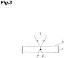
- the laser light L is relatively moved along the part 5 (i.e., in the direction of arrow A in Fig. 2 ) while locating a converging point P within the object 1 as illustrated in Fig. 3 .
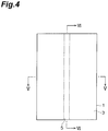
- This forms a modified region 7 within the object 1 along the part 5 as illustrated in Figs. 4 to 6 , whereby the modified region 7 becomes a removing region 8 to be removed by etching which will be explained later.
- the converging point P is a position at which the laser light L is converged.
- the part 5 may be curved instead of being straight, shaped into a three-dimensional form combining them, or specified in terms of coordinates.
- the modified region 7 may be formed either continuously or intermittently.
- the modified region 7 may be formed like lines or dots. It will be sufficient if the modified region 7 is formed at least within the object 1. There are cases where fractures are formed from the modified region 7 acting as a start point, and the fractures and modified region 7 may be exposed at outer surfaces (the front face, rear face, and outer peripheral face) of the object 1.
- the laser light L is absorbed in particular in the vicinity of the converging point within the object 1 while being transmitted therethrough, whereby the modified region 7 is formed in the object 1 (i.e., internal absorption type laser processing).
- the processing region gradually progresses from the front face 3 side to the rear face side in general.
- the modified region 7 in accordance with this embodiment means regions whose physical characteristics such as density, refractive index, and mechanical strength have attained states different from those of their surroundings.
- Examples of the modified region 7 include molten processed regions, crack regions, dielectric breakdown regions, refractive index changed regions, and their mixed regions.
- Further examples of the modified region 7 include an area where the density has changed from that of an unmodified region in a material of the object 1 and an area formed with a lattice defect (which may collectively be referred to as a high-density transitional region).
- the molten processed regions, refractive index changed regions, areas where the modified region 7 has a density different from that of the unmodified region, or areas formed with a lattice defect may further incorporate a fracture (cut or microcrack) therewithin or at an interface between the modified region 7 and an unmodified region.
- the incorporated fracture may be formed over the whole surface of the modified region 7 or in only a part or a plurality of parts thereof. Examples of the object 1 include those containing or constituted by silicon.
- this embodiment forms the modified region 7 in the object 1 and then etches the object 1, so as to advance the etching selectively along the modified region 7 (i.e., along the modified region 7, fractures included in the modified region 7, or fractures from the modified region 7), thereby removing a part extending along the modified region 7 in the object 1.
- fractures are also known as cracks, microcracks, fractures, and the like (hereinafter simply referred to as "fractures").
- etching for example, a capillary action or the like is utilized so that fractures included in the modified region 7 of the object 1 or fractures from the modified region 7 are impregnated with an etchant, so as to advance (develop) the etching along fracture surfaces.
- etching rate of the modified region 7 itself is high, the etching is selectively advanced along the modified region 7, so as to remove it.
- etching examples include a case where the object 1 is immersed in the etchant (dipping) and a case where the object 1 is coated with the etchant while being rotated (spin etching).
- the etchant examples include KOH (potassium hydroxide), TMAH (aqueous tetramethylammonium hydroxide solution), EDP (ethylenediamine pyrocatechol), NaOH (sodium hydroxide), CsOH (cesium hydroxide), NH 4 OH (ammonium hydroxide), and hydrazine.
- the etchant to be used is not limited to liquids but may be in the form of a gel (jelly or semisolid).
- the etchant is used at a temperature ranging from ambient temperature to about 100°C, which is set appropriately according to a required etching rate or the like. When etching Si with KOH, for example, the temperature is preferably about 60°C.
- this embodiment performs anisotropic etching which is etching having a higher (or lower) etching rate in a specific direction.
- the anisotropic etching is applicable not only to relatively thin objects but also to thick ones (having a thickness of 800 ⁇ m to 100 ⁇ m, for example).
- the etching can be advanced along the modified region 7. That is, the anisotropic etching here enables not only the etching of the plane direction in conformity to the crystal orientation, but also the etching independent of the crystal orientation.
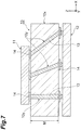
- Fig. 7 is a schematic sectional view illustrating the interposer manufactured by this embodiment
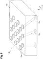
- Fig. 8 is a schematic perspective view of the interposer of Fig. 7
- the manufacturing method of this embodiment manufactures an interposer as a relay board for electrically connecting electronic components to each other.
- an interposer 10 is a silicon interposer comprising a substrate 10x and a plurality of through-hole electrodes 10y provided in the substrate 10x. As illustrated in Fig. 7 , this interposer 10 constitutes connection wiring between a semiconductor device 11 such as an IC chip and a flexible cable (flexible printed board) 12, while converting their wiring pitches.
- the substrate 10x is made of silicon and formed like a flat sheet having a target thickness M which is 200 ⁇ m, for example.
- the through-hole electrodes 10y each including a conductor 13 and pads 14, electrically connect the front and rear sides of the substrate 10x to each other.
- a plurality of through-hole electrodes 10y are arranged in a staggered manner as seen from the front face of the substrate 10x. That is, the plurality of through-hole electrodes 10y are arranged such that a pair of through-hole electrodes 10y close to each other in the Y direction are shifted from each other by a half pitch, for example, in the X direction.
- Figs. 9 to 12 are flow diagrams illustrating the interposer manufacturing method in accordance with this embodiment. As illustrated in Figs. 9 to 12 , this embodiment converges the laser light L at the object 1, so as to form modified regions 7 within the object 1. Then, predetermined parts on the front face 3 side and rear face 21 side of the object 1 are removed as removing parts 1p by anisotropic etching, so as to thin the object 1 to the target thickness M. At the same time, the etching is selectively advanced along the modified regions 7, so as to form a plurality of through holes 24.
- the object 1 is a sheet-like silicon substrate which is transparent to the wavelength (e.g., 1064 nm) of the laser light L with which it is irradiated.
- the object 1 has a thickness of 300 ⁇ m, for example, which is greater than the target thickness M.
- the object 1 has the front face 3 and rear face 21 (main faces), which are (100) planes.
- parts 5 are programmably set as being specified by three-dimensional coordinates.
- the parts 5 have first part to form a modified region 5x and second part to form a modified region 5y.
- the first parts 5x are set along the parts corresponding to the through holes 24 (see Fig. 12(c) ) within the object 1.
- the first parts 5x herein include first part 5x 1 extending in the thickness direction of the object 1, first part 5x 2 tilted with respect to the thickness direction, and first part 5x 3 tilted with respect to the thickness direction by a greater angle than the first part 5x 2 .
- the first part 5x 2 , 5x 3 extend along (111) planes of the object 1.
- the second parts 5y are set in the removing parts 1p on the front face 3 side and rear face 21 side within the object 1.
- a plurality of second parts 5y are set so as to join with both ends of the first part 5x, respectively, and extend parallel to the thickness direction of the object 1.
- the thickness direction of the object 1 (irradiation direction of the laser light L) to be the Z direction
- the object 1 is mounted on the mount table with the front face 3 facing up. Subsequently, as illustrated in Fig. 9(b) , a converging point of the laser light L (hereinafter simply referred to as “converging point”) is located at the removing part 1p on the rear face 21 side within the object 1. Then, while relatively moving the converging point in the X direction, irradiation with the laser light L (hereinafter simply referred to as "scan”) is performed in an on/off manner from the front face 3 side such that modified regions 7 are formed in the parts 5. This forms the modified regions 7 at respective positions on the second parts 5y in the removing part 1p on the rear face 21 side.
- scan irradiation with the laser light L
- modified regions 7 formed thereby are constituted by modified spots.
- formed modified regions 7 include fractures generated from the modified regions 7 (ditto in the following modified regions 7).
- modified regions 7 joining on the front face 3 side with the existing modified regions 7 are newly formed at respective positions on the second parts 5y in the removing part 1p on the rear face 21 side.
- modified regions 71 extending parallel to the Z direction i.e., extending substantially linearly along the Z direction so as not to intersect the Z direction
- the above-mentioned scan is repeatedly performed while progressively changing the position of the converging point in the Z direction from the rear face 21 side to the front face 3 side.
- This forms modified regions 72 joining with the existing modified regions 71 in the parts corresponding to the through holes 24 within the object 1, and modified regions 73 joining with the existing modified regions 72 and extending parallel to the Z direction (i.e., extending substantially linearly along the Z direction so as not to intersect the Z direction) within the removing part 1p on the front face 3 side.
- the modified regions 72 as the first modified regions extending in conformity to the through holes 24 are formed in the parts other than the removing parts 1p within the object 1, while the modified regions 71, 73 as the second modified regions joining with the respective end parts of the modified regions 72 and extending straight in the Z direction are formed in the removing parts 1p so as not to be exposed to the front face 3 and rear face 21.
- Figs. 9(a) to 11(b) mentioned above are repeatedly performed while changing the position of the converging point of the laser light L in the Y direction.
- the foregoing forms a plurality of modified regions 72 in conformity to a plurality of through holes 24 within the object 1, and a plurality of modified regions 71, 73 joining with their corresponding modified regions 72 and extending parallel to the Z direction within the removing parts 1p.
- the modified regions 72 are formed along the first parts 5x 1 to 5x 3 and thus include modified regions 72 1 extending in the Z direction, modified regions 72 2 tilted in the X direction with respect to the Z direction, and modified regions 72 2 tilted in the same direction by a greater angle than the modified regions 72 3 .
- the sizes, lengths, and the like of the modified regions 71, 73 are made such that the etching time required for thinning the object 1 to the target thickness M and the total of the respective etching times for etching the modified regions 71 to 73 equal each other in anisotropic etching in a later stage.
- the object 1 is etched for 60 min with KOH at 85°C, for example, as an etchant. This gradually removes the removing parts 1p in the object 1 from the front face 3 side and rear face 21 side, thereby progressively thinning the object 1. Then, when the object 1 is thinned until the modified regions 71, 73 are exposed as illustrated in Fig. 12(a) , the modified regions 71, 73 are impregnated with the etchant, whereby etching starts along the modified regions 71, 73. Subsequently, while the object 1 is thinned, its inside is selectively etched away along the modified regions 71, 73.
- the etchant infiltrates from the modified regions 71, 73 into the modified regions 72, whereby the etching starts to progress along the modified regions 72. Subsequently, while the object 1 is thinned, the inside of the object 1 is selectively etched away along the modified regions 72.
- the etching advances in the modified regions 72. Then, when the thickness of the object 1 becomes the target thickness M as illustrated in Fig. 12(c) , the object 1 is penetrated along the modified regions 72, whereby the forming of a plurality of through holes 24 completes.
- the plurality of through holes 24 are arranged so as to correspond to the above-mentioned through-hole electrodes 10y. Specifically, the plurality of through holes 24 are arranged in a staggered manner as seen from the front face 3 of the object 1. That is, in the plurality of through holes 24, the through holes 24 aligning in the X direction, which is their tilted direction, are staggered in the Y direction perpendicular to the tilted direction as seen from the front face 3. In other words, when seen from the front face 3, a group of through holes 24 arranged in the X direction align in the Y direction while shifting in the X direction.
- the plurality of through holes 24 are arranged such that a pair of through holes 24, 24 close to each other in the Y direction shift from each other by a half pitch in the X direction, for example.
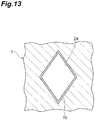
- the (111) planes of the object 1 are harder to etch (have a lower etching rate). Therefore, in the modified regions 72 extending along the (111) planes, the etching advances favorably, so that the inner faces of the resulting through holes 24 become smooth surfaces with less depressions and projections. As illustrated in Fig. 13 , the through holes 24 have substantially rectangular (diamond-shaped) cross sections, while varying less in inner sizes along their axes.
- the through holes 24 are formed along the modified regions 72 1 to 72 2 , respectively, and thus include through holes 24 1 extending in the Z direction, through holes 24 2 tilted in the X direction with respect to the Z direction, and through holes 24 3 tilted in the same direction by a greater angle than the through holes 24 2 .
- the object 1 is oxidized by wet oxidation or the like, so as to produce an electrically insulating oxide film on the inner face (inner wall) of each through hole 24.
- the inner face of the through hole 24 is a smooth surface, while its cross section is substantially rectangular, so that projections where the insulating film is hard to grow do not exist on the inner face of the through hole 24, whereby a uniform insulating film 15 can be formed, so as to suppress defects in the insulating film 15.
- the through holes 24 aligning in the X direction are staggered in the Y direction when seen from the front face 3 of the object 1 in this embodiment. Therefore, a plurality of through holes 24 and, as a consequence, a plurality of through-hole electrodes 10y can be arranged denser than in the case where the plurality of through holes are arranged into a simple lattice as seen from the front face 3, for example, whereby the resulting interposer 10 can be made smaller. This can also increase the numbers of through holes 24 and through-hole electrodes 10y that can be formed in the object 1, thereby achieving a higher wiring density in the interposer 10.
- the through hole 24 can be formed with a rectangular cross section, the insulating film 15 can be made uniform, so as to suppress defects in the insulating film 15, thereby securing electric conduction in the through-hole electrode 10y and preventing connections from failing, thus attaining high reliability.
- the etching for the modified regions 72 does not begin to progress when the object 1 is at the target thickness, but is induced to start to advance by the modified regions 71, 73 formed in the removing parts 1p when thinning the object 1 to the target thickness M by anisotropic etching, and the forming of the through holes 24 completes when the object 1 is thinned to the target thickness M.
- This can inhibit the opening sides (front face 3 side and rear face 21 side) of the through holes 24 from being removed in excess and increasing their aperture sizes (opening sizes) on the opening sides and inner widths, whereby the through holes 24 can be formed accurately in the object 1 having the target thickness M.
- this embodiment can form desirable through holes 24 while adjusting the thickness of the object 1.
- the modified regions 71, 73 for guiding the etching to the modified regions 72 are formed in the removing parts 1p, whereby the forming of the through holes 24 can be completed at the time of thinning to the target thickness M in anisotropic etching in a later stage.
- the thickness of the object 1 and the aperture size of the through holes 24 can be controlled accurately at the same time, so that appropriately forming the modified regions 71, 73, for example, can adjust the time required for penetrating the modified regions 72, whereby the final thickness of the substrate 10x can be set.
- modified regions 71, 73 extend parallel to the Z direction as mentioned above, it becomes easier to specify and manage the converging point of the laser light L when forming the modified regions 71, 73, whereby the laser processing can be facilitated.
- Fig. 14(a) is an enlarged sectional view illustrating a part of the object after forming modified regions therein
- Fig. 14(b) is an enlarged sectional view illustrating a part of the object after forming through holes therein.
- the aperture size H on the opening side of the through hole 24 2 formed by anisotropic etching is relatively small in conformity to the size of the modified regions 73.
- the aperture size H' on the opening side of the resulting through hole 24 2 ' is larger than the aperture size H. Therefore, when reducing the aperture size H on the opening side of the through hole 24, it is preferred for the modified regions 73 (71) formed in the removing part 1p to extend parallel to the Z direction.
- this embodiment can inhibit the etching of the modified regions 72 from advancing in excess when the object 1 attains the target thickness M and thereby increasing the aperture size on the opening side of the through hole 24 and its inner width.
- this embodiment repeatedly performs the scan along the X direction while changing the depth position of the converging point in the Z direction (see Figs. 9(b) to 11(b) ; first step) and repeatedly performs the same while changing the position of the converging point in the Y direction (second step), thereby forming a plurality of through holes 24.
- This can restrain the converging point from moving uselessly and enables rapid processing, thereby shortening the takt time (processing time) and lowering the cost.
- the interposer 10 in accordance with this embodiment has the through-hole electrodes 10y tilted with respect to the Z direction, which makes it unnecessary to stack a plurality of substrates 10x for changing wiring pitches, whereby its weight, thickness, and cost can be reduced. In addition, this can simplify the wiring and attain very fine wiring pitches, so as to facilitate designing and lower the electric resistance in wiring.
- this embodiment can enhance heat dissipation while restraining the wiring from breaking under the influence of thermal expansion differences when the semiconductor device 11 is made of silicon.
- this embodiment can remove the modified regions 7 and fractures incorporated therein from the object 1 after the processing by anisotropic etching and thus can improve its strength and quality. Since no cutting dusts occur during processing, an environment-friendly processing method can be achieved.
- the laser light entrance surface for forming the modified regions 7 is not limited to the front face 3 of the object 1, but may be the rear face 21 of the object 1.
- the modified regions 71, 73 respectively joining with the modified regions 72 on the rear face 21 side and the front face 3 side are formed in the removing parts 1p as those guiding the etching to the modified regions 72 in the above-mentioned embodiment, one of them may be formed alone.
- modified regions 71, 73 extending parallel to the Z direction are formed such as to join with the respective end parts of the modified regions 72 in the above-mentioned embodiment, the modified regions 71, 73 are not limited to those extending parallel to the Z direction, but may extend along the modified regions 72, for example.
- parallel encompasses those substantially parallel and those intended to become parallel.
- the direction and order of scans in the above-mentioned embodiment are not limited.
- the scan along the X direction may be repeatedly performed while changing the position of the converging point in the Y direction, and the same may be repeatedly performed while changing the depth position of the converging point in the Z direction, so as to form a plurality of through holes 24.
- irradiation with the laser light L may be performed while moving its converging point along one through hole 24 so as to form a modified region 7, and the same may be repeated by the number of through holes 24, so as to form a plurality of through holes 24.
- the on/off irradiation with the laser light L in the above-mentioned embodiment may be performed not only by controlling the on/off of the emission of the laser light L, but also by opening/closing a shutter disposed on the optical path of the laser light L or by masking on/off the front face 3 of the object 1, for example.
- the intensity of the laser light L may be controlled between an intensity at a threshold for forming the modified regions 7 (processing threshold) or higher and an intensity lower than the processing threshold.
- the above-mentioned embodiment can adjust the etchant (e.g., add additives such as alcohols and surfactants), so as to change the etchant rate in a specific crystal orientation, thereby forming a through hole having a desirable rectangular cross-sectional form (inner wall form).
- etchant e.g., add additives such as alcohols and surfactants
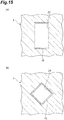
- anisotropic etching with an etchant doped with IPA isopropyl alcohol
- anisotropic etching with an etchant doped with a surfactant can make a through hole 24 with a square cross section as illustrated in Fig. 15(b) .
- the interposer 10 convert wiring pitches and pitches of the plurality of through-hole electrodes 10y on the front face is different from ones on the rear face in the above-mentioned embodiment, the above-mentioned embodiment can manufacture a interposer 50 as illustrated in Fig. 16 .
- pitches of the plurality of through-hole electrodes 10y on the front face and ones on the rear face equal each other, arrangement pattern of through-hole electrodes 10y on the front face and on the rear face equal each other. That is, the plurality of through-hole electrodes 10y are arranged in a staggered manner on the front face and on the rear face as seen in the Z direction. Here, horizontal position of the through-hole electrodes 10y are different each other between on the front face and on the rear face of the substrate 10. That is to say, the through-hole electrodes 10y are provided so as to arrange the same pattern and shift in the X direction or/and Y direction between on the front face and on the rear face.
- the present invention can provide a method for manufacturing an interposer which can be made smaller while securing high reliability.
Landscapes
- Engineering & Computer Science (AREA)
- Optics & Photonics (AREA)
- Physics & Mathematics (AREA)
- Mechanical Engineering (AREA)
- Plasma & Fusion (AREA)
- Chemical Kinetics & Catalysis (AREA)
- General Chemical & Material Sciences (AREA)
- Chemical & Material Sciences (AREA)
- Oil, Petroleum & Natural Gas (AREA)
- Manufacturing & Machinery (AREA)
- Microelectronics & Electronic Packaging (AREA)
- Laser Beam Processing (AREA)
- Particle Formation And Scattering Control In Inkjet Printers (AREA)
Claims (5)
- Verfahren zur Herstellung eines Interposers, der mit mehreren Durchgangselektroden ausgestattet ist, wobei das Verfahren umfasst:einen Laserlichtbündelungsschritt des Bündelns eines Laserlichtes (L) auf einem zu verarbeitenden blattartigen Gegenstand (1) aus Silizium, um einen modifizierten Bereich (7, 71, 72, 73) innerhalb des Gegenstandes auszubilden;einen Ätzschritt des anisotropen Ätzens des Gegenstandes nach dem Laserlichtbündelungsschritt, um das Ätzen selektiv entlang des modifizierten Bereiches (7, 71, 72, 73) fortzusetzen und eine Vielzahl von Durchgangslöchern (24) in dem Gegenstand auszubilden, wobei die Durchgangslöcher der Vielzahl von Durchgangslöchern (24) in Bezug auf die Dickenrichtung des Gegenstandes geneigt sind und jedes Durchgangsloch einen rechteckigen oder jedes Durchgangsloch einen länglichen oder jedes Durchgangsloch einen quadratischen Querschnitt hat;einen Isolierfilm-Ausbildungsschritt des Ausbildens eines Isolierfilms (15) auf einer Innenwand jedes Durchgangslochs nach dem Ätzschritt; undeinen Durchgangslochelektroden-Ausbildungsschritt des Einfügens eines Leiters in die Durchgangslöcher, um so die Durchgangslochelektroden (10y) nach dem Isolierfilm-Ausbildungsschritt auszubilden;dadurch gekennzeichnet, dassdie Vielzahl der Durchgangslöcher, wenn sie von einer Hauptfläche (10x, 3) des Gegenstandes betrachtet werden, so angeordnet sind, dass die Durchgangslöcher, die in der geneigten Richtung angeordnet sind, in einer Richtung ausgerichtet sind, die senkrecht zu der geneigten Richtung ist, wobei sie in der geneigten Richtung in gestaffelter Weise verschoben sind.
- Verfahren für die Herstellung eines Interposers gemäß Anspruch 1, bei dem der Laserlichtbündelungsschritt einen ersten modifizierten Bereich (72) als den modifizierten Bereich in einem Teil entsprechend dem Durchgangsloch (24) in dem Gegenstand und einen zweiten modifizierten Bereich (71, 73) als den modifizierten Bereich ausbildet, der mit dem ersten modifizierten Bereich in einem Teil (1p) in Verbindung steht, der beim Ausdünnen durch das anisotrope Ätzen entfernt werden soll; und
der Ätzschritt das Ätzen selektiv entlang des zweiten modifizierten Bereichs und dann entlang des ersten modifizierten Bereichs fortsetzt, wodurch der Gegenstand auf eine Solldicke (M) ausgedünnt wird, und das Ausbilden der Durchgangslöcher abschließt, wenn der Gegenstand die Solldicke hat. - Verfahren zur Herstellung eines Interposers nach Anspruch 1 oder 2, bei dem sich der zweite modifizierte Bereich (71, 73) parallel zur Dickenrichtung des Gegenstandes erstreckt.
- Verfahren zur Herstellung eines Interposers nach einem der Ansprüche 1 bis 3, bei dem der Gegenstand eine Hauptfläche (3, 21) hat, die eine Ebene (100) ist.
- Verfahren zur Herstellung eines Interposers nach einem der Ansprüche 1 bis 4, bei dem der Laserlichtbündelungsschritt umfasst:einen ersten Schritt, der wiederholt einen Schritt des Bestrahlens des Gegenstandes mit dem Laserlicht ausführt, während ein Bündelungspunkt des Laserlichts (L) relativ entlang einer ersten Richtung orthogonal zu einer Laserlichtbestrahlungsrichtung bewegt wird, während eine Tiefenposition des Bündelungspunktes in Bestrahlungsrichtung verändert wird; undeinen zweiten Schritt, der wiederholt den ersten Schritt durchführt, während eine Position des Bündelungspunktes in einer zweiten Richtung senkrecht zu der Bestrahlungsrichtung und einer ersten Richtung verändert wird.
Applications Claiming Priority (2)
| Application Number | Priority Date | Filing Date | Title |
|---|---|---|---|
| JP2010167405 | 2010-07-26 | ||
| PCT/JP2011/066349 WO2012014718A1 (ja) | 2010-07-26 | 2011-07-19 | インターポーザの製造方法 |
Publications (3)
| Publication Number | Publication Date |
|---|---|
| EP2600397A1 EP2600397A1 (de) | 2013-06-05 |
| EP2600397A4 EP2600397A4 (de) | 2016-12-21 |
| EP2600397B1 true EP2600397B1 (de) | 2019-08-21 |
Family
ID=45529934
Family Applications (1)
| Application Number | Title | Priority Date | Filing Date |
|---|---|---|---|
| EP11812310.8A Active EP2600397B1 (de) | 2010-07-26 | 2011-07-19 | Verfahren zur herstellung einer zwischenschaltung |
Country Status (7)
| Country | Link |
|---|---|
| US (1) | US8841213B2 (de) |
| EP (1) | EP2600397B1 (de) |
| JP (1) | JP5509332B2 (de) |
| KR (1) | KR101880148B1 (de) |
| CN (1) | CN103026486B (de) |
| TW (1) | TWI539496B (de) |
| WO (1) | WO2012014718A1 (de) |
Families Citing this family (18)
| Publication number | Priority date | Publication date | Assignee | Title |
|---|---|---|---|---|
| JP5574866B2 (ja) * | 2010-07-26 | 2014-08-20 | 浜松ホトニクス株式会社 | レーザ加工方法 |
| JP2013187247A (ja) * | 2012-03-06 | 2013-09-19 | Nippon Hoso Kyokai <Nhk> | インターポーザおよびその製造方法 |
| ES2908956T3 (es) * | 2013-04-04 | 2022-05-04 | Lpkf Laser & Electronics Ag | Procedimiento para introducir rupturas en un sustrato |
| WO2014161535A2 (de) * | 2013-04-04 | 2014-10-09 | Lpkf Laser & Electronics Ag | Verfahren und vorrichtung zum trennen eines substrates |
| KR101459483B1 (ko) | 2013-10-07 | 2014-11-07 | 현대자동차 주식회사 | 차량용 변속장치 |
| KR20170044143A (ko) * | 2014-09-16 | 2017-04-24 | 엘피케이에프 레이저 앤드 일렉트로닉스 악티엔게젤샤프트 | 판 모양의 작업물 안으로 적어도 하나의 컷아웃부 또는 구멍을 도입하기 위한 방법 |
| US10410883B2 (en) | 2016-06-01 | 2019-09-10 | Corning Incorporated | Articles and methods of forming vias in substrates |
| US10794679B2 (en) | 2016-06-29 | 2020-10-06 | Corning Incorporated | Method and system for measuring geometric parameters of through holes |
| US10134657B2 (en) | 2016-06-29 | 2018-11-20 | Corning Incorporated | Inorganic wafer having through-holes attached to semiconductor wafer |
| US11078112B2 (en) | 2017-05-25 | 2021-08-03 | Corning Incorporated | Silica-containing substrates with vias having an axially variable sidewall taper and methods for forming the same |
| US10580725B2 (en) | 2017-05-25 | 2020-03-03 | Corning Incorporated | Articles having vias with geometry attributes and methods for fabricating the same |
| WO2019109251A1 (zh) * | 2017-12-05 | 2019-06-13 | 深圳市为通博科技有限责任公司 | 光路调制器及其制作方法、指纹识别装置和终端设备 |
| US12180108B2 (en) | 2017-12-19 | 2024-12-31 | Corning Incorporated | Methods for etching vias in glass-based articles employing positive charge organic molecules |
| US11554984B2 (en) | 2018-02-22 | 2023-01-17 | Corning Incorporated | Alkali-free borosilicate glasses with low post-HF etch roughness |
| US11344972B2 (en) | 2019-02-11 | 2022-05-31 | Corning Incorporated | Laser processing of workpieces |
| KR102432339B1 (ko) * | 2019-11-19 | 2022-08-16 | 한국전자통신연구원 | 경사 전극을 이용한 인터포저 및 그 제조 방법 |
| US12313890B2 (en) * | 2021-06-16 | 2025-05-27 | Intel Corporation | Through-substrate optical vias |
| US20230197620A1 (en) * | 2021-12-21 | 2023-06-22 | Intel Corporation | Methods, systems, apparatus, and articles of manufacture for integrated circuit package substrates with high aspect ratio through glass vias |
Family Cites Families (50)
| Publication number | Priority date | Publication date | Assignee | Title |
|---|---|---|---|---|
| JPH04150212A (ja) | 1990-10-09 | 1992-05-22 | Seiko Epson Corp | 水晶基板のエッチング加工方法 |
| JPH0740482A (ja) | 1993-07-27 | 1995-02-10 | Jsp Corp | 発泡ポリプロピレン系樹脂積層体及び該積層体の製造方法 |
| JP2873937B2 (ja) | 1996-05-24 | 1999-03-24 | 工業技術院長 | ガラスの光微細加工方法 |
| JP3473668B2 (ja) | 1997-01-23 | 2003-12-08 | セイコーエプソン株式会社 | インクジェット式記録ヘッド |
| JPH11167945A (ja) | 1997-12-04 | 1999-06-22 | Shin Etsu Polymer Co Ltd | 電気コネクタおよびその製造方法 |
| JP4497147B2 (ja) | 1998-12-16 | 2010-07-07 | セイコーエプソン株式会社 | 半導体チップの製造方法、半導体装置の製造方法、回路基板の製造方法及び電子機器の製造方法 |
| KR20010042981A (ko) * | 1999-02-25 | 2001-05-25 | 야스카와 히데아키 | 레이저를 이용한 피가공물의 가공 방법 |
| JP4659300B2 (ja) | 2000-09-13 | 2011-03-30 | 浜松ホトニクス株式会社 | レーザ加工方法及び半導体チップの製造方法 |
| JP4880820B2 (ja) | 2001-01-19 | 2012-02-22 | 株式会社レーザーシステム | レーザ支援加工方法 |
| CN101335235B (zh) | 2002-03-12 | 2010-10-13 | 浜松光子学株式会社 | 基板的分割方法 |
| KR20030076274A (ko) * | 2002-03-18 | 2003-09-26 | 도레 엔지니아린구 가부시키가이샤 | 비접촉 아이디 카드류 및 그 제조방법 |
| CA2428187C (en) | 2002-05-08 | 2012-10-02 | National Research Council Of Canada | Method of fabricating sub-micron structures in transparent dielectric materials |
| JP4329374B2 (ja) | 2002-07-29 | 2009-09-09 | パナソニック電工株式会社 | 発光素子およびその製造方法 |
| JP4158481B2 (ja) | 2002-10-21 | 2008-10-01 | セイコーエプソン株式会社 | レーザー加工方法およびその装置、並びにその装置を用いた穴あけ加工方法 |
| JP2004160618A (ja) | 2002-11-15 | 2004-06-10 | Seiko Epson Corp | マイクロマシン及びマイクロマシンの製造方法 |
| JP2004223586A (ja) | 2003-01-24 | 2004-08-12 | Institute Of Physical & Chemical Research | 透明材料内部の処理方法 |
| JP4160851B2 (ja) * | 2003-03-31 | 2008-10-08 | 富士通株式会社 | 指紋認識用半導体装置 |
| JP2004304130A (ja) | 2003-04-01 | 2004-10-28 | Seiko Epson Corp | 半導体装置の製造方法 |
| JP2004351494A (ja) | 2003-05-30 | 2004-12-16 | Seiko Epson Corp | レーザーに対して透明な材料の穴あけ加工方法 |
| JP2004359475A (ja) | 2003-06-02 | 2004-12-24 | Seiko Epson Corp | 光学素子の製造方法及び光学装置 |
| JP4385656B2 (ja) | 2003-06-11 | 2009-12-16 | セイコーエプソン株式会社 | 液体噴射ヘッド、及び、その製造方法 |
| JP4182841B2 (ja) | 2003-08-28 | 2008-11-19 | セイコーエプソン株式会社 | 単結晶基板の加工方法 |
| JP2005121915A (ja) | 2003-10-16 | 2005-05-12 | Seiko Epson Corp | マイクロレンズ用凹部付き基板の製造方法、マイクロレンズ用凹部付き基板、マイクロレンズ基板、液晶パネル用対向基板、液晶パネルおよび投射型表示装置 |
| JP2005121916A (ja) | 2003-10-16 | 2005-05-12 | Seiko Epson Corp | レンチキュラレンズ用凹部付き基板の製造方法、レンチキュラレンズ用凹部付き基板、レンチキュラレンズ基板、透過型スクリーンおよびリア型プロジェクタ |
| JP2005144586A (ja) | 2003-11-13 | 2005-06-09 | Seiko Epson Corp | 構造体の製造方法、液滴吐出ヘッド、液滴吐出装置 |
| JP2005144622A (ja) | 2003-11-18 | 2005-06-09 | Seiko Epson Corp | 構造体の製造方法、液滴吐出ヘッド、液滴吐出装置 |
| JP2005152693A (ja) | 2003-11-20 | 2005-06-16 | Seiko Epson Corp | 構造体の製造方法、液滴吐出ヘッド、液滴吐出装置 |
| JP2005169993A (ja) | 2003-12-15 | 2005-06-30 | Canon Inc | インクジェット記録ヘッドおよびインクジェット記録ヘッドの製造方法 |
| JP2005208175A (ja) | 2004-01-20 | 2005-08-04 | Seiko Epson Corp | 光部品及びその製造方法、光モジュール、光通信装置、電子機器 |
| JP2005206401A (ja) | 2004-01-21 | 2005-08-04 | Seiko Epson Corp | 構造体の製造方法、液滴吐出ヘッド及び液滴吐出装置 |
| JP2005306702A (ja) | 2004-04-26 | 2005-11-04 | Namiki Precision Jewel Co Ltd | テーパー形状を有する微小穴の形成方法 |
| JP4955935B2 (ja) * | 2004-05-25 | 2012-06-20 | キヤノン株式会社 | 貫通孔形成方法および半導体装置の製造方法 |
| JP2005351774A (ja) | 2004-06-10 | 2005-12-22 | Seiko Epson Corp | マイクロアレイ作製用ヘッドの製造方法、マイクロアレイ作製用ヘッドおよびマイクロアレイ作製用装置 |
| US7390740B2 (en) * | 2004-09-02 | 2008-06-24 | Micron Technology, Inc. | Sloped vias in a substrate, spring-like contacts, and methods of making |
| JP4630971B2 (ja) | 2004-12-21 | 2011-02-09 | 並木精密宝石株式会社 | パルスレーザによる微小構造の形成方法 |
| JP2006290630A (ja) | 2005-02-23 | 2006-10-26 | Nippon Sheet Glass Co Ltd | レーザを用いたガラスの加工方法 |
| JP2007036758A (ja) | 2005-07-27 | 2007-02-08 | Seiko Epson Corp | Atカット水晶振動片、その製造方法、及び水晶デバイス |
| JP2007096246A (ja) * | 2005-08-30 | 2007-04-12 | Kyocera Corp | 配線基板およびそれを用いた電子装置 |
| JP4564434B2 (ja) * | 2005-09-30 | 2010-10-20 | Okiセミコンダクタ株式会社 | 半導体装置及び半導体装置の製造方法 |
| JP2007101833A (ja) | 2005-10-04 | 2007-04-19 | Seiko Epson Corp | マイクロレンズの製造方法、マイクロレンズ、空間光変調装置、スクリーン及びプロジェクタ |
| US7824560B2 (en) * | 2006-03-07 | 2010-11-02 | Canon Kabushiki Kaisha | Manufacturing method for ink jet recording head chip, and manufacturing method for ink jet recording head |
| JP4854336B2 (ja) * | 2006-03-07 | 2012-01-18 | キヤノン株式会社 | インクジェットヘッド用基板の製造方法 |
| US7804175B2 (en) * | 2007-01-31 | 2010-09-28 | Hewlett-Packard Development Company, L.P. | Semiconductor structures including conductive vias continuously extending therethrough and methods of making the same |
| WO2008146744A1 (ja) | 2007-05-25 | 2008-12-04 | Hamamatsu Photonics K.K. | 切断用加工方法 |
| US8197705B2 (en) * | 2007-09-06 | 2012-06-12 | Canon Kabushiki Kaisha | Method of processing silicon substrate and method of manufacturing liquid discharge head |
| KR20090058462A (ko) * | 2007-12-04 | 2009-06-09 | 가부시키가이샤 에바라 세이사꾸쇼 | 도전재료 구조체의 형성방법 및 도금장치 및 도금방법 |
| CN102422414A (zh) * | 2009-04-28 | 2012-04-18 | 株式会社藤仓 | 器件安装构造以及器件安装方法 |
| WO2011048858A1 (ja) * | 2009-10-23 | 2011-04-28 | 株式会社フジクラ | デバイス実装構造およびデバイス実装方法 |
| WO2011048862A1 (ja) * | 2009-10-23 | 2011-04-28 | 株式会社フジクラ | デバイス実装構造およびデバイス実装方法 |
| JP5574866B2 (ja) * | 2010-07-26 | 2014-08-20 | 浜松ホトニクス株式会社 | レーザ加工方法 |
-
2011
- 2011-07-19 EP EP11812310.8A patent/EP2600397B1/de active Active
- 2011-07-19 US US13/389,050 patent/US8841213B2/en not_active Expired - Fee Related
- 2011-07-19 WO PCT/JP2011/066349 patent/WO2012014718A1/ja not_active Ceased
- 2011-07-19 CN CN201180036871.3A patent/CN103026486B/zh not_active Expired - Fee Related
- 2011-07-19 KR KR1020127031689A patent/KR101880148B1/ko not_active Expired - Fee Related
- 2011-07-19 JP JP2012526432A patent/JP5509332B2/ja active Active
- 2011-07-26 TW TW100126374A patent/TWI539496B/zh not_active IP Right Cessation
Non-Patent Citations (1)
| Title |
|---|
| None * |
Also Published As
| Publication number | Publication date |
|---|---|
| CN103026486A (zh) | 2013-04-03 |
| JP5509332B2 (ja) | 2014-06-04 |
| KR101880148B1 (ko) | 2018-07-20 |
| TW201220370A (en) | 2012-05-16 |
| CN103026486B (zh) | 2016-08-03 |
| WO2012014718A1 (ja) | 2012-02-02 |
| EP2600397A1 (de) | 2013-06-05 |
| JPWO2012014718A1 (ja) | 2013-09-12 |
| KR20130119320A (ko) | 2013-10-31 |
| US8841213B2 (en) | 2014-09-23 |
| US20120142186A1 (en) | 2012-06-07 |
| TWI539496B (zh) | 2016-06-21 |
| EP2600397A4 (de) | 2016-12-21 |
Similar Documents
| Publication | Publication Date | Title |
|---|---|---|
| EP2600397B1 (de) | Verfahren zur herstellung einer zwischenschaltung | |
| EP2599581B1 (de) | Laserverarbeitungsverfahren | |
| US8673167B2 (en) | Laser processing method | |
| US8961806B2 (en) | Laser processing method | |
| US8741777B2 (en) | Substrate processing method | |
| EP2600390B1 (de) | Chip-herstellungsverfahren | |
| EP2599582A1 (de) | Substratverarbeitungsverfahren | |
| EP2599578B1 (de) | Laserverarbeitungsverfahren zur herstellung eines durchgangslochs | |
| US8828873B2 (en) | Method for manufacturing semiconductor device | |
| EP2600392B1 (de) | Laserverarbeitungsverfahren |
Legal Events
| Date | Code | Title | Description |
|---|---|---|---|
| PUAI | Public reference made under article 153(3) epc to a published international application that has entered the european phase |
Free format text: ORIGINAL CODE: 0009012 |
|
| 17P | Request for examination filed |
Effective date: 20130222 |
|
| AK | Designated contracting states |
Kind code of ref document: A1 Designated state(s): AL AT BE BG CH CY CZ DE DK EE ES FI FR GB GR HR HU IE IS IT LI LT LU LV MC MK MT NL NO PL PT RO RS SE SI SK SM TR |
|
| DAX | Request for extension of the european patent (deleted) | ||
| RA4 | Supplementary search report drawn up and despatched (corrected) |
Effective date: 20161123 |
|
| RIC1 | Information provided on ipc code assigned before grant |
Ipc: H01L 21/48 20060101ALI20161117BHEP Ipc: B23K 26/00 20140101ALN20161117BHEP Ipc: H01L 23/498 20060101AFI20161117BHEP |
|
| STAA | Information on the status of an ep patent application or granted ep patent |
Free format text: STATUS: EXAMINATION IS IN PROGRESS |
|
| 17Q | First examination report despatched |
Effective date: 20180627 |
|
| REG | Reference to a national code |
Ref country code: DE Ref legal event code: R079 Ref document number: 602011061479 Country of ref document: DE Free format text: PREVIOUS MAIN CLASS: H01L0023120000 Ipc: H01L0023498000 |
|
| GRAP | Despatch of communication of intention to grant a patent |
Free format text: ORIGINAL CODE: EPIDOSNIGR1 |
|
| STAA | Information on the status of an ep patent application or granted ep patent |
Free format text: STATUS: GRANT OF PATENT IS INTENDED |
|
| RIC1 | Information provided on ipc code assigned before grant |
Ipc: B23K 26/00 20140101ALN20190213BHEP Ipc: H01L 21/48 20060101ALI20190213BHEP Ipc: H01L 23/498 20060101AFI20190213BHEP |
|
| INTG | Intention to grant announced |
Effective date: 20190308 |
|
| GRAS | Grant fee paid |
Free format text: ORIGINAL CODE: EPIDOSNIGR3 |
|
| GRAA | (expected) grant |
Free format text: ORIGINAL CODE: 0009210 |
|
| STAA | Information on the status of an ep patent application or granted ep patent |
Free format text: STATUS: THE PATENT HAS BEEN GRANTED |
|
| AK | Designated contracting states |
Kind code of ref document: B1 Designated state(s): AL AT BE BG CH CY CZ DE DK EE ES FI FR GB GR HR HU IE IS IT LI LT LU LV MC MK MT NL NO PL PT RO RS SE SI SK SM TR |
|
| REG | Reference to a national code |
Ref country code: GB Ref legal event code: FG4D |
|
| REG | Reference to a national code |
Ref country code: CH Ref legal event code: EP |
|
| REG | Reference to a national code |
Ref country code: DE Ref legal event code: R096 Ref document number: 602011061479 Country of ref document: DE |
|
| REG | Reference to a national code |
Ref country code: AT Ref legal event code: REF Ref document number: 1170726 Country of ref document: AT Kind code of ref document: T Effective date: 20190915 |
|
| REG | Reference to a national code |
Ref country code: IE Ref legal event code: FG4D |
|
| REG | Reference to a national code |
Ref country code: LT Ref legal event code: MG4D |
|
| REG | Reference to a national code |
Ref country code: NL Ref legal event code: MP Effective date: 20190821 |
|
| PG25 | Lapsed in a contracting state [announced via postgrant information from national office to epo] |
Ref country code: PT Free format text: LAPSE BECAUSE OF FAILURE TO SUBMIT A TRANSLATION OF THE DESCRIPTION OR TO PAY THE FEE WITHIN THE PRESCRIBED TIME-LIMIT Effective date: 20191223 Ref country code: NO Free format text: LAPSE BECAUSE OF FAILURE TO SUBMIT A TRANSLATION OF THE DESCRIPTION OR TO PAY THE FEE WITHIN THE PRESCRIBED TIME-LIMIT Effective date: 20191121 Ref country code: NL Free format text: LAPSE BECAUSE OF FAILURE TO SUBMIT A TRANSLATION OF THE DESCRIPTION OR TO PAY THE FEE WITHIN THE PRESCRIBED TIME-LIMIT Effective date: 20190821 Ref country code: BG Free format text: LAPSE BECAUSE OF FAILURE TO SUBMIT A TRANSLATION OF THE DESCRIPTION OR TO PAY THE FEE WITHIN THE PRESCRIBED TIME-LIMIT Effective date: 20191121 Ref country code: FI Free format text: LAPSE BECAUSE OF FAILURE TO SUBMIT A TRANSLATION OF THE DESCRIPTION OR TO PAY THE FEE WITHIN THE PRESCRIBED TIME-LIMIT Effective date: 20190821 Ref country code: LT Free format text: LAPSE BECAUSE OF FAILURE TO SUBMIT A TRANSLATION OF THE DESCRIPTION OR TO PAY THE FEE WITHIN THE PRESCRIBED TIME-LIMIT Effective date: 20190821 Ref country code: HR Free format text: LAPSE BECAUSE OF FAILURE TO SUBMIT A TRANSLATION OF THE DESCRIPTION OR TO PAY THE FEE WITHIN THE PRESCRIBED TIME-LIMIT Effective date: 20190821 Ref country code: SE Free format text: LAPSE BECAUSE OF FAILURE TO SUBMIT A TRANSLATION OF THE DESCRIPTION OR TO PAY THE FEE WITHIN THE PRESCRIBED TIME-LIMIT Effective date: 20190821 |
|
| PG25 | Lapsed in a contracting state [announced via postgrant information from national office to epo] |
Ref country code: AL Free format text: LAPSE BECAUSE OF FAILURE TO SUBMIT A TRANSLATION OF THE DESCRIPTION OR TO PAY THE FEE WITHIN THE PRESCRIBED TIME-LIMIT Effective date: 20190821 Ref country code: ES Free format text: LAPSE BECAUSE OF FAILURE TO SUBMIT A TRANSLATION OF THE DESCRIPTION OR TO PAY THE FEE WITHIN THE PRESCRIBED TIME-LIMIT Effective date: 20190821 Ref country code: RS Free format text: LAPSE BECAUSE OF FAILURE TO SUBMIT A TRANSLATION OF THE DESCRIPTION OR TO PAY THE FEE WITHIN THE PRESCRIBED TIME-LIMIT Effective date: 20190821 Ref country code: GR Free format text: LAPSE BECAUSE OF FAILURE TO SUBMIT A TRANSLATION OF THE DESCRIPTION OR TO PAY THE FEE WITHIN THE PRESCRIBED TIME-LIMIT Effective date: 20191122 Ref country code: IS Free format text: LAPSE BECAUSE OF FAILURE TO SUBMIT A TRANSLATION OF THE DESCRIPTION OR TO PAY THE FEE WITHIN THE PRESCRIBED TIME-LIMIT Effective date: 20191221 Ref country code: LV Free format text: LAPSE BECAUSE OF FAILURE TO SUBMIT A TRANSLATION OF THE DESCRIPTION OR TO PAY THE FEE WITHIN THE PRESCRIBED TIME-LIMIT Effective date: 20190821 |
|
| REG | Reference to a national code |
Ref country code: AT Ref legal event code: MK05 Ref document number: 1170726 Country of ref document: AT Kind code of ref document: T Effective date: 20190821 |
|
| PG25 | Lapsed in a contracting state [announced via postgrant information from national office to epo] |
Ref country code: TR Free format text: LAPSE BECAUSE OF FAILURE TO SUBMIT A TRANSLATION OF THE DESCRIPTION OR TO PAY THE FEE WITHIN THE PRESCRIBED TIME-LIMIT Effective date: 20190821 |
|
| PG25 | Lapsed in a contracting state [announced via postgrant information from national office to epo] |
Ref country code: IT Free format text: LAPSE BECAUSE OF FAILURE TO SUBMIT A TRANSLATION OF THE DESCRIPTION OR TO PAY THE FEE WITHIN THE PRESCRIBED TIME-LIMIT Effective date: 20190821 Ref country code: DK Free format text: LAPSE BECAUSE OF FAILURE TO SUBMIT A TRANSLATION OF THE DESCRIPTION OR TO PAY THE FEE WITHIN THE PRESCRIBED TIME-LIMIT Effective date: 20190821 Ref country code: PL Free format text: LAPSE BECAUSE OF FAILURE TO SUBMIT A TRANSLATION OF THE DESCRIPTION OR TO PAY THE FEE WITHIN THE PRESCRIBED TIME-LIMIT Effective date: 20190821 Ref country code: EE Free format text: LAPSE BECAUSE OF FAILURE TO SUBMIT A TRANSLATION OF THE DESCRIPTION OR TO PAY THE FEE WITHIN THE PRESCRIBED TIME-LIMIT Effective date: 20190821 Ref country code: AT Free format text: LAPSE BECAUSE OF FAILURE TO SUBMIT A TRANSLATION OF THE DESCRIPTION OR TO PAY THE FEE WITHIN THE PRESCRIBED TIME-LIMIT Effective date: 20190821 Ref country code: RO Free format text: LAPSE BECAUSE OF FAILURE TO SUBMIT A TRANSLATION OF THE DESCRIPTION OR TO PAY THE FEE WITHIN THE PRESCRIBED TIME-LIMIT Effective date: 20190821 |
|
| PG25 | Lapsed in a contracting state [announced via postgrant information from national office to epo] |
Ref country code: IS Free format text: LAPSE BECAUSE OF FAILURE TO SUBMIT A TRANSLATION OF THE DESCRIPTION OR TO PAY THE FEE WITHIN THE PRESCRIBED TIME-LIMIT Effective date: 20200224 Ref country code: CZ Free format text: LAPSE BECAUSE OF FAILURE TO SUBMIT A TRANSLATION OF THE DESCRIPTION OR TO PAY THE FEE WITHIN THE PRESCRIBED TIME-LIMIT Effective date: 20190821 Ref country code: SK Free format text: LAPSE BECAUSE OF FAILURE TO SUBMIT A TRANSLATION OF THE DESCRIPTION OR TO PAY THE FEE WITHIN THE PRESCRIBED TIME-LIMIT Effective date: 20190821 Ref country code: SM Free format text: LAPSE BECAUSE OF FAILURE TO SUBMIT A TRANSLATION OF THE DESCRIPTION OR TO PAY THE FEE WITHIN THE PRESCRIBED TIME-LIMIT Effective date: 20190821 |
|
| REG | Reference to a national code |
Ref country code: DE Ref legal event code: R097 Ref document number: 602011061479 Country of ref document: DE |
|
| PLBE | No opposition filed within time limit |
Free format text: ORIGINAL CODE: 0009261 |
|
| STAA | Information on the status of an ep patent application or granted ep patent |
Free format text: STATUS: NO OPPOSITION FILED WITHIN TIME LIMIT |
|
| PG2D | Information on lapse in contracting state deleted |
Ref country code: IS |
|
| 26N | No opposition filed |
Effective date: 20200603 |
|
| PG25 | Lapsed in a contracting state [announced via postgrant information from national office to epo] |
Ref country code: SI Free format text: LAPSE BECAUSE OF FAILURE TO SUBMIT A TRANSLATION OF THE DESCRIPTION OR TO PAY THE FEE WITHIN THE PRESCRIBED TIME-LIMIT Effective date: 20190821 |
|
| REG | Reference to a national code |
Ref country code: DE Ref legal event code: R119 Ref document number: 602011061479 Country of ref document: DE |
|
| PG25 | Lapsed in a contracting state [announced via postgrant information from national office to epo] |
Ref country code: MC Free format text: LAPSE BECAUSE OF FAILURE TO SUBMIT A TRANSLATION OF THE DESCRIPTION OR TO PAY THE FEE WITHIN THE PRESCRIBED TIME-LIMIT Effective date: 20190821 |
|
| REG | Reference to a national code |
Ref country code: CH Ref legal event code: PL |
|
| GBPC | Gb: european patent ceased through non-payment of renewal fee |
Effective date: 20200719 |
|
| REG | Reference to a national code |
Ref country code: BE Ref legal event code: MM Effective date: 20200731 |
|
| PG25 | Lapsed in a contracting state [announced via postgrant information from national office to epo] |
Ref country code: GB Free format text: LAPSE BECAUSE OF NON-PAYMENT OF DUE FEES Effective date: 20200719 Ref country code: FR Free format text: LAPSE BECAUSE OF NON-PAYMENT OF DUE FEES Effective date: 20200731 Ref country code: LU Free format text: LAPSE BECAUSE OF NON-PAYMENT OF DUE FEES Effective date: 20200719 Ref country code: CH Free format text: LAPSE BECAUSE OF NON-PAYMENT OF DUE FEES Effective date: 20200731 Ref country code: LI Free format text: LAPSE BECAUSE OF NON-PAYMENT OF DUE FEES Effective date: 20200731 |
|
| PG25 | Lapsed in a contracting state [announced via postgrant information from national office to epo] |
Ref country code: DE Free format text: LAPSE BECAUSE OF NON-PAYMENT OF DUE FEES Effective date: 20210202 Ref country code: BE Free format text: LAPSE BECAUSE OF NON-PAYMENT OF DUE FEES Effective date: 20200731 |
|
| PG25 | Lapsed in a contracting state [announced via postgrant information from national office to epo] |
Ref country code: IE Free format text: LAPSE BECAUSE OF NON-PAYMENT OF DUE FEES Effective date: 20200719 |
|
| PG25 | Lapsed in a contracting state [announced via postgrant information from national office to epo] |
Ref country code: MT Free format text: LAPSE BECAUSE OF FAILURE TO SUBMIT A TRANSLATION OF THE DESCRIPTION OR TO PAY THE FEE WITHIN THE PRESCRIBED TIME-LIMIT Effective date: 20190821 Ref country code: CY Free format text: LAPSE BECAUSE OF FAILURE TO SUBMIT A TRANSLATION OF THE DESCRIPTION OR TO PAY THE FEE WITHIN THE PRESCRIBED TIME-LIMIT Effective date: 20190821 |
|
| PG25 | Lapsed in a contracting state [announced via postgrant information from national office to epo] |
Ref country code: MK Free format text: LAPSE BECAUSE OF FAILURE TO SUBMIT A TRANSLATION OF THE DESCRIPTION OR TO PAY THE FEE WITHIN THE PRESCRIBED TIME-LIMIT Effective date: 20190821 |