EP2643866B1 - Organische elektrolumineszenzvorrichtung - Google Patents
Organische elektrolumineszenzvorrichtung Download PDFInfo
- Publication number
- EP2643866B1 EP2643866B1 EP11808815.2A EP11808815A EP2643866B1 EP 2643866 B1 EP2643866 B1 EP 2643866B1 EP 11808815 A EP11808815 A EP 11808815A EP 2643866 B1 EP2643866 B1 EP 2643866B1
- Authority
- EP
- European Patent Office
- Prior art keywords
- group
- substituted
- unsubstituted
- carbon atoms
- ring
- Prior art date
- Legal status (The legal status is an assumption and is not a legal conclusion. Google has not performed a legal analysis and makes no representation as to the accuracy of the status listed.)
- Active
Links
- 0 CC=CC=C1*2CCCC1C2 Chemical compound CC=CC=C1*2CCCC1C2 0.000 description 5
Images


Classifications
-
- H—ELECTRICITY
- H10—SEMICONDUCTOR DEVICES; ELECTRIC SOLID-STATE DEVICES NOT OTHERWISE PROVIDED FOR
- H10K—ORGANIC ELECTRIC SOLID-STATE DEVICES
- H10K50/00—Organic light-emitting devices
- H10K50/10—OLEDs or polymer light-emitting diodes [PLED]
- H10K50/11—OLEDs or polymer light-emitting diodes [PLED] characterised by the electroluminescent [EL] layers
- H10K50/125—OLEDs or polymer light-emitting diodes [PLED] characterised by the electroluminescent [EL] layers specially adapted for multicolour light emission, e.g. for emitting white light
- H10K50/13—OLEDs or polymer light-emitting diodes [PLED] characterised by the electroluminescent [EL] layers specially adapted for multicolour light emission, e.g. for emitting white light comprising stacked EL layers within one EL unit
- H10K50/131—OLEDs or polymer light-emitting diodes [PLED] characterised by the electroluminescent [EL] layers specially adapted for multicolour light emission, e.g. for emitting white light comprising stacked EL layers within one EL unit with spacer layers between the electroluminescent layers
-
- H—ELECTRICITY
- H10—SEMICONDUCTOR DEVICES; ELECTRIC SOLID-STATE DEVICES NOT OTHERWISE PROVIDED FOR
- H10K—ORGANIC ELECTRIC SOLID-STATE DEVICES
- H10K50/00—Organic light-emitting devices
- H10K50/10—OLEDs or polymer light-emitting diodes [PLED]
- H10K50/17—Carrier injection layers
- H10K50/171—Electron injection layers
-
- H—ELECTRICITY
- H10—SEMICONDUCTOR DEVICES; ELECTRIC SOLID-STATE DEVICES NOT OTHERWISE PROVIDED FOR
- H10K—ORGANIC ELECTRIC SOLID-STATE DEVICES
- H10K50/00—Organic light-emitting devices
- H10K50/10—OLEDs or polymer light-emitting diodes [PLED]
- H10K50/18—Carrier blocking layers
-
- H—ELECTRICITY
- H10—SEMICONDUCTOR DEVICES; ELECTRIC SOLID-STATE DEVICES NOT OTHERWISE PROVIDED FOR
- H10K—ORGANIC ELECTRIC SOLID-STATE DEVICES
- H10K85/00—Organic materials used in the body or electrodes of devices covered by this subclass
-
- H—ELECTRICITY
- H10—SEMICONDUCTOR DEVICES; ELECTRIC SOLID-STATE DEVICES NOT OTHERWISE PROVIDED FOR
- H10K—ORGANIC ELECTRIC SOLID-STATE DEVICES
- H10K85/00—Organic materials used in the body or electrodes of devices covered by this subclass
- H10K85/60—Organic compounds having low molecular weight
- H10K85/649—Aromatic compounds comprising a hetero atom
- H10K85/654—Aromatic compounds comprising a hetero atom comprising only nitrogen as heteroatom
-
- H—ELECTRICITY
- H10—SEMICONDUCTOR DEVICES; ELECTRIC SOLID-STATE DEVICES NOT OTHERWISE PROVIDED FOR
- H10K—ORGANIC ELECTRIC SOLID-STATE DEVICES
- H10K85/00—Organic materials used in the body or electrodes of devices covered by this subclass
- H10K85/60—Organic compounds having low molecular weight
- H10K85/649—Aromatic compounds comprising a hetero atom
- H10K85/657—Polycyclic condensed heteroaromatic hydrocarbons
- H10K85/6572—Polycyclic condensed heteroaromatic hydrocarbons comprising only nitrogen in the heteroaromatic polycondensed ring system, e.g. phenanthroline or carbazole
-
- H—ELECTRICITY
- H10—SEMICONDUCTOR DEVICES; ELECTRIC SOLID-STATE DEVICES NOT OTHERWISE PROVIDED FOR
- H10K—ORGANIC ELECTRIC SOLID-STATE DEVICES
- H10K85/00—Organic materials used in the body or electrodes of devices covered by this subclass
- H10K85/60—Organic compounds having low molecular weight
- H10K85/649—Aromatic compounds comprising a hetero atom
- H10K85/657—Polycyclic condensed heteroaromatic hydrocarbons
- H10K85/6574—Polycyclic condensed heteroaromatic hydrocarbons comprising only oxygen in the heteroaromatic polycondensed ring system, e.g. cumarine dyes
-
- C—CHEMISTRY; METALLURGY
- C09—DYES; PAINTS; POLISHES; NATURAL RESINS; ADHESIVES; COMPOSITIONS NOT OTHERWISE PROVIDED FOR; APPLICATIONS OF MATERIALS NOT OTHERWISE PROVIDED FOR
- C09K—MATERIALS FOR MISCELLANEOUS APPLICATIONS, NOT PROVIDED FOR ELSEWHERE
- C09K2211/00—Chemical nature of organic luminescent or tenebrescent compounds
- C09K2211/10—Non-macromolecular compounds
- C09K2211/1018—Heterocyclic compounds
- C09K2211/1025—Heterocyclic compounds characterised by ligands
- C09K2211/1029—Heterocyclic compounds characterised by ligands containing one nitrogen atom as the heteroatom
-
- C—CHEMISTRY; METALLURGY
- C09—DYES; PAINTS; POLISHES; NATURAL RESINS; ADHESIVES; COMPOSITIONS NOT OTHERWISE PROVIDED FOR; APPLICATIONS OF MATERIALS NOT OTHERWISE PROVIDED FOR
- C09K—MATERIALS FOR MISCELLANEOUS APPLICATIONS, NOT PROVIDED FOR ELSEWHERE
- C09K2211/00—Chemical nature of organic luminescent or tenebrescent compounds
- C09K2211/10—Non-macromolecular compounds
- C09K2211/1018—Heterocyclic compounds
- C09K2211/1025—Heterocyclic compounds characterised by ligands
- C09K2211/1044—Heterocyclic compounds characterised by ligands containing two nitrogen atoms as heteroatoms
-
- H—ELECTRICITY
- H10—SEMICONDUCTOR DEVICES; ELECTRIC SOLID-STATE DEVICES NOT OTHERWISE PROVIDED FOR
- H10K—ORGANIC ELECTRIC SOLID-STATE DEVICES
- H10K2101/00—Properties of the organic materials covered by group H10K85/00
- H10K2101/30—Highest occupied molecular orbital [HOMO], lowest unoccupied molecular orbital [LUMO] or Fermi energy values
-
- H—ELECTRICITY
- H10—SEMICONDUCTOR DEVICES; ELECTRIC SOLID-STATE DEVICES NOT OTHERWISE PROVIDED FOR
- H10K—ORGANIC ELECTRIC SOLID-STATE DEVICES
- H10K2101/00—Properties of the organic materials covered by group H10K85/00
- H10K2101/40—Interrelation of parameters between multiple constituent active layers or sublayers, e.g. HOMO values in adjacent layers
Definitions
- the present invention relates to an organic electroluminescence device.
- organic electroluminescence device (hereinafter, referred to as organic EL device) can be classified by the emission principle into two types: a fluorescent EL device and a phosphorescent EL device.
- a voltage is applied to the organic EL device, holes are injected from an anode and electrons are injected from a cathode. The holes and the electrons are recombined in an emitting layer to form excitons.
- the electron spin statistics theory singlet excitons and triplet excitons are generated at a ratio of 25% : 75%.
- a voltage applied at the maximum efficiency was about 4 to 6 V.
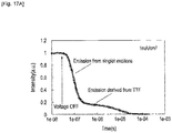
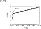
- Non-Patent Literature 1 a non-doped device, in which an anthracene compound is used as a host, is analyzed. A mechanism is found that singlet excitons are generated by collision and fusion of two triplet excitons, whereby fluorescent emission is increased. Such a phenomenon in which singlet excitons are generated by collision and fusion of two triplet excitons is hereinafter referred to as TTF (Triplet-Triplet Fusion) phenomenon.
- TTF Triplet-Triplet Fusion
- Non-Patent Literature 2 discloses a blue-emission fluorescent OLED in which a layer of an aromatic compound (efficiency-enhancement layer, referred to as EEL) is interposed between an emitting layer including a host and a dopant and an electron transporting layer. It is reported that an OLED in which a compound EEL-1 is used as EEL is driven by a low voltage, exhibits a high external quantum efficiency and has a long lifetime compared with an OLED in which BPhen or BCP is used as EEL. This EEL can serve as a blocking layer for causing a TTF phenomenon.
- EEL aromatic compound
- Document EP2166588 (A ) discloses a light emitting device comprising an emitting layer and a blocking layer, wherein the blocking layer comprises an aromatic heterocyclic derivative, and the triplet energy ETb (eV) of the aromatic heterocyclic derivative is larger than the triplet enegry ETh (eV) of the host, and the aromatic heterocyclic derivative comprises an azine ring; and the triplet energy ETd (eV) of the fluorescetn dopant is larger than the triplet energy ETh (eV) of the host.
- Document KR20070115588 discloses an organic electroluminescent device comprising anthracene deriveative as a host and pyrene derivative as a dopant in the light emitting layer.
- Non-Patent Literature 1 discloses only that fluorescent emission is increased by collision and fusion of triplet excitons in a non-doped device in which only a host is used. In this technology, an increase in efficiency by triplet excitons is as low as 3% to 6%.
- Non-Patent Literature 2 reports that the external quantum efficiency (EQE) of the device using BCP as EEL is inferior to a device using EEL-1 as EEL by tens of %. It has been considered difficult to satisfy a predetermined relationship of triplet energy and to efficiently cause a TTF phenomenon by using a compound (e.g. BCP) including a hetero atom in a blocking layer, thereby preparing a highly efficient device.
- EQE external quantum efficiency
- An object of the invention is to provide an organic EL device of a fluorescent emission with high efficiency.
- the inventors has found out that the efficiency can be improved even in an organic EL device structured with an electron transporting zone including the specific compound having an azine ring without an electron injecting layer, in which the specific compound serves as an electron injecting layer.
- an organic electroluminescence device including in sequential order an anode, an emitting layer, an electron transporting zone, and a cathode, in which the emitting layer includes a host and a fluorescent dopant, a blocking layer is adjacent to the emitting layer in the electron transporting zone, the blocking layer includes an aromatic heterocyclic derivative, a triplet energy E T b (eV) of the aromatic heterocyclic derivative is larger than a triplet energy E T h (eV) of the host, and the aromatic heterocyclic derivative has an azine ring.
- the aromatic heterocyclic derivative contained in the blocking layer has an azine ring.
- An aromatic heterocyclic derivative not according to the invention has an azine structure represented by the general formula (AZ-1).
- X independently represents N (a nitrogen atom) or CR.
- CR represents R bonded to C (a carbon atom).
- two or three X are preferably N.
- the azine structure represented by the general formula (AZ-1) is further preferably a pyrimidine structure or 1,3,5-triazine structure.
- R independently represents a substituted or unsubstituted alkyl group, substituted or unsubstituted cycloalkyl group, substituted or unsubstituted aryl group, substituted or unsubstituted heterocyclic group, or a substituent formed by linking a plurality thereof.
- the aromatic heterocyclic derivative is represented by a formula (BL-21) below.
- HAr represents a substituted or unsubstituted heterocyclic group having 5 to 30 ring atoms. When a plurality of HAr are present, the plurality of HAr may be the same or different.
- Az represents a substituted or unsubstituted pyrimidine, a substituted or unsubstituted pyrazine, a substituted or unsubstituted pyridazine, or a substituted or unsubstituted triazine.
- L represents a single bond, a divalent to tetravalent residue of a substituted or unsubstituted aromatic hydrocarbon ring having 6 to 30 ring carbon atoms, a divalent to tetravalent residue of a substituted or unsubstituted heterocyclic ring having 5 to 30 ring atoms, or a divalent to tetravalent residue of a group in which two or three rings selected from the aromatic hydrocarbon ring and the heterocyclic ring are combined in a single bond.
- a is an integer of 1 to 3.
- b is an integer of 1 to 3.
- an electron mobility of the aromatic heterocyclic derivative is 10 -6 at least cm 2 /Vs in an electric field intensity of 0.04 MV/cm to 0.5 MV/cm.
- the triplet energy E T b (eV) of the aromatic heterocyclic derivative and the triplet energy E T h (eV) of the host satisfy a relationship of E T h +0.2 ⁇ E T b .
- the triplet energy E T b (eV) of the aromatic heterocyclic derivative and the triplet energy E T h (eV) of the host satisfy a relationship of E T h +0.3 ⁇ E T b .
- the triplet energy E T b (eV) of the aromatic heterocyclic derivative and the triplet energy E T h (eV) of the host satisfy a relationship of E T h +0.4 ⁇ E T b .
- an electron injecting layer is adjacent to the blocking layer in the electron transporting zone.
- the electron injecting layer includes a material that has an electron mobility of at least 10 -6 cm 2 /Vs in an electric field intensity of 0.04 MV/cm to 0.5 MV/cm.
- the fluorescent dopant exhibits a fluorescent emission of a main peak wavelength of less than or equal to 550 nm, and the triplet energy E T d (eV) of the fluorescent dopant is larger than the triplet energy E T h (eV) of the host.
- a hole transporting zone is positioned between the anode and the emitting layer, a hole transporting layer is adjacent to the emitting layer in the hole transporting zone, the hole transporting layer comprising an aromatic amine derivative represented by any of formulae (a-1) to (a-5) specified in claim 1.
- the electron injecting layer and the blocking layer are formed of the same material.
- the electron injecting layer and the blocking layer are formed of the same material, and the electron injecting layer is doped with a donor.
- the fluorescent dopant is a pyrene derivative.
- the host is an anthracene derivative.
- the host is a compound that comprises a double bond only in a cyclic structure.
- the fluorescent dopant is a pyrene derivative, which preferably contains a double bond only in a cyclic structure.
- an organic electroluminescence device including in sequential order an anode, an emitting layer, an electron transporting zone, and a cathode, in which the emitting layer includes a host and a fluorescent dopant, a blocking layer is adjacent to the emitting layer in the electron transporting zone, the blocking layer includes an aromatic heterocyclic derivative, a triplet energy E T b (eV) of the aromatic heterocyclic derivative is larger than a triplet energy E T h (eV) of the host, the aromatic heterocyclic derivative has an azine ring, in applied voltage at the maximum current efficiency (cd/A), luminous intensity derived from single excitons generated by collision of triplet excitons generated in the emitting layer accounts for 30% or more of the entire luminous intensity.
- the emitting layer includes a host and a fluorescent dopant
- a blocking layer is adjacent to the emitting layer in the electron transporting zone
- the blocking layer includes an aromatic heterocyclic derivative
- the TTF phenomenon efficiently occurs, thereby providing an organic EL device of a fluorescent emission with a high efficiency.
- the invention utilizes a TTF phenomenon.
- the TTF phenomenon will be initially described below.
- triplet excitons (hereinafter abbreviated as 3 A*) collide with one another with an increase in the density thereof, whereby a reaction shown by the following formula occurs.
- 1 A represents the ground state and 1 A* represents the lowest singlet excitons.
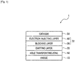
- Fig. 1 is schematic view showing one example of an organic EL device according to a first exemplary embodiment of the invention.
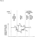
- Fig. 2 is a view showing a relationship between a triplet energy of the emitting layer and a triplet energy of an electron transporting zone in the organic EL device according to the first exemplary embodiment.
- the triplet energy is referred to as a difference between energy in the lowest triplet state and energy in the ground state.
- the singlet energy (often referred to as energy gap) is referred to as a difference between energy in the lowest singlet state and energy in the ground state.
- the organic EL device 1 shown in Fig. 1 includes an anode 10, a hole transporting zone 60, an emitting layer 20, a blocking layer 30, an electron injecting layer 40, and a cathode 50 in sequential order. These components are adjacent to one another in the organic EL device of the invention.
- An electron transporting zone 70 includes the blocking layer 30 and the electron injecting layer 40. It is preferred that the hole transporting zone 60 is interposed between the anode 10 and the emitting layer 20.
- the hole transporting zone includes at least one of a hole injecting layer and a hole transporting layer.
- a simply-called blocking layer means a layer functioning as a barrier against triplet energy. Accordingly, the blocking layer functions differently from a hole blocking layer and a charge blocking layer.
- the electron transporting zone may not include an electron injecting layer, but a specific compound having an azine ring may serve as an electron injecting layer. Accordingly, in such a case, the electron transporting zone 70 in the organic EL device 1 shown in Fig. 1 may be provided with only the blocking layer 30, so that the blocking layer 30 is adjacent to the cathode 50.
- the emitting layer includes a host and a dopant.
- a dopant emitting fluorescent light of a main peak wavelength of 550 nm or less (hereinafter occasionally referred to as a fluorescent dopant having a main peak wavelength of 550 nm or less) is preferable.
- a main peak wavelength means a peak wavelength of luminescence spectrum exhibiting a maximum luminous intensity among luminous spectra measured in a toluene solution with a concentration from 10 -5 mol/liter to 10 -6 mol/liter.
- the main peak wavelength of 550 nm is substantially equivalent to a green emission. In this wavelength zone, improvement in luminous efficiency of a fluorescent device utilizing the TTF phenomenon is desired.
- a blue-emitting fluorescent device of 480 nm or less further improvement in luminous efficiency is expectable.
- a red-emitting fluorescent device of 550 nm or more a phosphorescent device exhibiting a high internal quantum efficiency has already been at a practical level. Accordingly, improvement in luminous efficiency as a fluorescent device is not desired.
- the holes injected from the anode are injected to the emitting layer via the hole transporting zone.
- the electrons injected from the cathode are injected to the emitting layer via the electron injecting layer and the blocking layer. Subsequently, the holes and the electrons are recombined in the emitting layer to generate singlet excitons and triplet excitons.
- recombination may occur either on host molecules or on dopant molecules.
- the blocking layer is adjacent to the emitting layer.
- the blocking layer has a function of preventing triplet excitons generated in the emitting layer to be diffused to an electron transporting zone and confining the triplet excitons within the emitting layer to increase a density of the triplet excitons therein, thereby causing the TTF phenomenon efficiently.
- the blocking layer also serves for efficiently injecting the electrons to the emitting layer.
- the density of the triplet excitons is decreased since the electron-hole recombination in the emitting layer is decreased.
- the frequency of collision of the triplet excitons is reduced, whereby the TTF phenomenon does not occur efficiently.
- the inventors have found that even a compound having a large optical energy gap has a function to receive electron injection from the electron injecting layer and further transport the electron when the compound includes an aromatic heterocyclic derivative having an azine ring in the blocking layer.
- the inventors also have found that electrons are easily injected from the aromatic heterocyclic derivative having the azine ring to a blue-emission fluorescent host material. It has typically been considered that a compound having a small affinity is used as an electron transporting layer to cause high voltage to be applied on a device.
- the inventors have found that smooth electron injection from the adjacent layer and smooth electron injection to the emitting layer can allow electron injection to the emitting layer without applying high voltage on the organic EL device and efficiently bring a TTF phenomenon.
- Fig. 4 shows one example of an energy band diagram of an organic EL device according to the first exemplary embodiment.
- the affinity A e of the electron injecting layer is larger than the affinity A b of the blocking layer.
- the aromatic heterocyclic derivative contained in the blocking layer has an azine ring.
- An aromatic heterocyclic derivative not according to the invention has an azine structure represented by the general formula (AZ-1).
- X independently represents N (a nitrogen atom) or CR.
- CR represents R bonded to C (a carbon atom).
- two or three X are preferably N.
- the azine structure represented by the general formula (AZ-1) is further preferably a pyrimidine structure or 1,3,5-triazine structure.
- R independently represents a substituted or unsubstituted alkyl group, substituted or unsubstituted cycloalkyl group, substituted or unsubstituted aryl group, substituted or unsubstituted heterocyclic group, or a substituent formed by linking a plurality thereof.
- a preferable example of the aromatic heterocyclic derivative that is contained in the blocking layer and has an azine ring is a compound represented by the following general formula (BL-21).
- HAr represents a substituted or unsubstituted heterocyclic group having 5 to 30 ring atoms, and when a plurality of HAr are present, the plurality of HAr are the same or different.
- HAr is preferably a substituted or unsubstituted heterocyclic group having 6 to 30 ring atoms.
- Az represents a substituted or unsubstituted azine, preferably a substituted or unsubstituted pyrimidine or substituted or unsubstituted triazine.
- L represents a single bond, a divalent to tetravalent residue of a substituted or unsubstituted aromatic hydrocarbon ring having 6 to 30 ring carbon atoms, a divalent to tetravalent residue of a substituted or unsubstituted heterocyclic ring having 5 to 30 ring atoms, or a divalent to tetravalent residue formed by combination in a single bond of two to three rings selected from the aromatic hydrocarbon ring and the heterocyclic ring.
- L is preferably a substituted or unsubstituted phenylene group, substituted or unsubstituted naphthalene group, or substituted or unsubstituted phenanthrene group. This arrangement is preferable because this arrangement provides a compound having a sufficient triplet energy to efficiently cause TTF, thereby realizing a highly efficient organic EL device.
- a is an integer of 1 to 3 and b is an integer of 1 to 3.
- Az has a structure represented by the following formula (BL-21-1).
- HAr is preferably a substituted or unsubstituted pyridyl group, substituted or unsubstituted pyrimidinyl group, substituted or unsubstituted pyrazinyl group, substituted or unsubstituted pyridazinyl group, substituted or unsubstituted triazinyl group, substituted or unsubstituted quinolinyl group, substituted or unsubstituted isoquinolinyl group, substituted or unsubstituted quinoxalinyl group, or heterocyclic groups listed in the formulae (BL-21-2).
- HAr preferably has a structure represented by the following (BL-21-2).
- Y is O, S, N(R') or C(R')(R').
- Z is N or C(R').
- Y is O, S, N(R') or C(R')(R').
- Z is N or C(R').
- the plurality of Y may be mutually the same or different.
- the plurality of Z may be mutually the same or different.
- the plurality of R' are included in each heterocyclic ring, the plurality of R' may be mutually the same or different.
- R' is used as a bonding portion with L and the rest of R' are independently a hydrogen atom, fluorine atom, substituted or unsubstituted alkyl group having 1 to 10 carbon atoms, substituted or unsubstituted cycloalkyl group having 3 to 8 ring carbon atoms, substituted silyl group having 3 to 30 carbon atoms, cyano group, substituted or unsubstituted alkoxy group having 1 to 20 carbon atoms, substituted or unsubstituted aryloxy group having 6 to 20 ring carbon atoms, substituted or unsubstituted aryl group having 6 to 30 ring carbon atoms, or substituted or unsubstituted heterocyclic group having 5 to 30 ring atoms.
- HAr has a structure represented by the following (BL-21-3).
- TTF efficiently occurs to provide a highly efficient organic EL device.
- all of Z are C(R'), in which R' is a hydrogen atom, an alkyl group having 1 to 4 carbon atoms or an aryl group having 6 to 12 ring carbon atoms.
- R' is a hydrogen atom, an alkyl group having 1 to 4 carbon atoms or an aryl group having 6 to 12 ring carbon atoms.
- HAr is preferably a carbazolyl group, a dibenzothiophenyl group and a dibenzofuranyl group.
- HAr is selected from a carbazolyl group, dibenzothiophenyl group and dibenzofuranyl group, electron injection to the emitting layer is promoted to provide an organic EL device that can be driven at low voltage with a high efficiency.
- HAr has a structure represented by the following (BL-21-4).
- TTF efficiently occurs to provide a highly efficient organic EL device.
- each heterocyclic ring When a plurality of Y or Z are included in each heterocyclic ring, the plurality of Y or Z may be mutually the same or different. When a plurality of R' are included in each heterocyclic ring, the plurality of R' may be mutually the same or different. In each heterocyclic ring, one of R' is used as a bonding portion with L.
- R' are independently a hydrogen atom, fluorine atom, substituted or unsubstituted alkyl group having 1 to 10 carbon atoms, substituted or unsubstituted cycloalkyl group having 3 to 8 ring carbon atoms, substituted silyl group having 3 to 30 carbon atoms, cyano group, substituted or unsubstituted alkoxy group having 1 to 20 carbon atoms, substituted or unsubstituted aryloxy group having 6 to 20 ring carbon atoms, substituted or unsubstituted aryl group having 6 to 30 ring carbon atoms, or substituted or unsubstituted heterocyclic group having 5 to 30 ring atoms.
- At least one of the plurality of Y is preferably O or S.
- a compound has a suitable mobility, so that TTF efficiently occurs to provide a highly efficient organic EL device.
- a is preferably an integer of 1 or 2
- b is preferably an integer of 1 or 2.
- aryl group examples are preferably a phenyl group, biphenyl group, o-terphenyl group, m-terphenyl group, p-terphenyl group, naphthyl group, phenanthryl group, chrysenyl group, benzophenanthrenyl group, benzochrysenyl group, benzanthryl group, triphenyl group, fluoranthenyl group, benzofluoranthenyl group and fluorenyl group, more preferably phenyl group, biphenyl group, naphthyl group, phenanthryl group.
- aryl group are a phenyl group, naphthyl group and phenanthryl group.
- a compound has sufficiently large triplet energy to efficiently cause TTF, so that a highly efficient organic EL device is achievable.
- heterocyclic group other than HAr are preferably a pyrizinyl group, pyrazinyl group, pyrimidinyl group, pyridazinyl group, triazinyl group, indolyl group, quinolinyl group, acridinyl group, pyrrolidinyl group, dioxanyl group, piperidinyl group, morpholyl group, piperazinyl group, carbazolyl group, furanyl group, thiophenyl group, oxazolyl group, oxadiazolyl group, benzooxazolyl group, thiazolyl group, thiadiazolyl group, benzothizolyl group, triazolyl group, imidazolyl group, benzoimidazolyl group, imidazopyridyl group, benzofuranyl group and dibenzofuranyl group.
- the dipole moment in a molecule in the blocking layer material when a dipole moment in a molecule in the blocking layer material is large, it is considered that an energy level is shifted in a direction in which an electron conduction level of the blocking layer material is raised for bonding to the blue-emission fluorescent emitting layer. It is considered that, when this shift raises the electron conduction level, energy block is generated at electron injection from the blocking layer to the blue-emission fluorescent emitting layer to increase a driving voltage of the device. Accordingly, in order to drive the organic EL device at a lower voltage, the dipole moment in the molecule of the blocking layer material is preferably small.
- a triplet energy T 1 of the aromatic heterocyclic derivative having the azine ring is preferably larger than 2.0 (eV), more preferably larger than 2.3 (eV). With this triplet energy T 1 , the function of the blocking layer is reinforced.
- the blocking layer preferably includes an aromatic heterocyclic derivative having a cyclic structure of six rings or more.
- the blocking layer has a ring structure of five rings or less, film stability at a thin film formation is low due to its small molecule size. This means that, when these compounds are used as the blocking layer, a condition of an interface between the blocking layer and the electron injecting layer is easily changed, resulting in partial association of molecules. Since the condition of the interface is changed by such association, it is considered that the electron supply from the electron injecting layer is hampered.
- one cyclic structure refers to a cyclic structure having one ring formed by a covalent bond of non-metal atoms in a molecule.
- the number of a fused cyclic structure is defined as the number of a cyclic structure of the fused ring group.
- a naphthalene ring has two cyclic structures and a dibenzofuran ring has three cyclic structures.
- An aromatic heterocyclic derivative represented by the following chemical formula (1) has ten cyclic structures.
- BAlq represented by the following chemical formula (2)
- an aromatic cyclic structure and a hetero cyclic structure which are directly bonded to metals or indirectly through an atom, are also counted as the cyclic structure. Accordingly, BAlq has six cyclic structures.
- Bphen represented by the following chemical formula (3) has five cyclic structures.
- a compound for the electron injecting layer is exemplified by a compound represented by the following formula (EIL-1).
- HAr 1 is a substituted or unsubstituted nitrogen-containing heterocyclic group, preferably having the following structures.
- Examples of a substituent for HAr 1 in the formula (EIL-1) includes a fluorine atom, cyano group, substituted or unsubstituted alkyl group having 1 to 20 carbon atoms, substituted or unsubstituted cycloalkyl group having 3 to 20 carbon atoms, substituted or unsubstituted alkylsilyl group having 3 to 20 carbon atoms, substituted or unsubstituted arylsilyl group having 8 to 30 carbon atoms, substituted or unsubstituted alkoxy group having 1 to 20 carbon atoms, substituted or unsubstituted aryloxy group having 6 to 30 carbon atoms, substituted or unsubstituted aryl group having 6 to 30 ring carbon atoms and substituted or unsubstituted heterocyclic group having 5 to 30 ring atoms.
- Ar 1 is a substituted or unsubstituted fused ring group having 10 to 30 ring carbon atoms, preferably having the following fused cyclic structures.
- Examples of a substituent for Ar 1 in the formula (EIL-1) includes a fluorine atom, cyano group, substituted or unsubstituted alkyl group having 1 to 20 carbon atoms, substituted or unsubstituted cycloalkyl group having 3 to 20 carbon atoms, substituted or unsubstituted alkylsilyl group having 3 to 20 carbon atoms, substituted or unsubstituted arylsilyl group having 8 to 30 carbon atoms, substituted or unsubstituted alkoxy group having 1 to 20 carbon atoms, substituted or unsubstituted aryloxy group having 6 to 30 carbon atoms, substituted or unsubstituted aryl group having 6 to 30 ring carbon atoms and substituted or unsubstituted heterocyclic group having 5 to 30 ring atoms.
- L 1 represents a single bond, substituted or unsubstituted (a+b)-valent hydrocarbon cyclic group having 6 to 30 ring carbon atoms, substituted or unsubstituted (a+b)-valent heterocyclic group having 5 to 30 ring atoms, substituted or unsubstituted hydrocarbon cyclic group having 6 to 30 ring carbon atoms, or (a+b)-valent group formed by linking a plurality of substituted or unsubstituted heterocyclic groups each having 5 to 30 ring atoms.
- Examples of a substituent for L 1 in the formula (EIL-1) includes a fluorine atom, cyano group, substituted or unsubstituted alkylsilyl group having 3 to 20 carbon atoms, substituted or unsubstituted arylsilyl group having 8 to 30 carbon atoms, substituted or unsubstituted aryl group having 6 to 30 ring carbon atoms and substituted or unsubstituted heterocyclic group having 5 to 30 ring atoms.
- a compound for the electron injecting layer is exemplified by a compound represented by the following formula (EIL-2).
- c is an integer of 2 to 4, preferably c is 2.
- Ar 108 represents a hydrogen atom, alkyl group having 1 to 20 carbon atoms or substituted or unsubstituted aryl group having 6 to 30 ring carbon atoms, more preferably a methyl group, t-butyl group, substituted or unsubstituted phenyl group or substituted or unsubstituted naphthyl group.
- the dopant used in this exemplary embodiment is a dopant emitting fluorescent light of a main peak wavelength of 550 nm or less (hereinafter occasionally referred to as a fluorescent dopant having a main peak wavelength of 550 nm or less).
- the dopant exhibits a relatively large energy gap. Accordingly, when the relationship of A h >A d is satisfied, a relationship of Ih>Id is simultaneously satisfied. Consequently, the dopant easily functions as a hole trap.
- Fig. 5 shows an Ip-Af relationship of the host and the dopant in the emitting layer in the above case.
- a shaded area in the emitting layer shows an exciton-density distribution.
- Figs. 6 to 8 shows the relationship in the case of A h >A b >A e .
- the hole transporting layer is adjacent to the emitting layer in the hole transporting zone and a triplet energy E T ho of the hole transporting layer is larger than a triplet energy E T h of the host.
- the dopant has a hole-trapping property
- the holes injected from the hole transporting zone to the emitting layer are trapped by the dopant. Accordingly, recombination often occurs in the emitting layer near the anode.
- a typically-known hole transporting material used for the hole transporting zone often exhibits a larger triplet energy than the host. Accordingly, diffusion of the triplet excitons on holes-side has not been a problem.
- recombination areas are a carrier mobility, ionization potential, affinity and film thickness of each of the hole transporting zone and the electron transporting zone. For instance, when the film thickness of the hole transporting zone is thicker than that of the electron transporting zone, an amount of the electrons injected to the emitting layer is relatively decreased. As a result, the recombination areas are shifted near the electron transporting zone. In such a case, when the blocking layer having a large triplet energy as in the invention is used, the TTF phenomenon can be efficiently induced.
- the host and the dopant that satisfy the above relationship in the affinity are selected from, for instance, the following compounds (see JP-A-2010-50227 (Japanese Patent Application No. 2008-212102 )).
- the host is an anthracene derivative.
- the dopant is a pyrene derivative.
- An aminoanthracene derivative is exemplified by a compound represented by the following formula (4).
- a 1 and A 2 independently represent a substituted or unsubstituted aliphatic hydrocarbon group having 1 to 6 carbon atoms, substituted or unsubstituted aromatic hydrocarbon group having 6 to 20 ring carbon atoms, or substituted or unsubstituted heterocyclic aromatic hydrocarbon group having 5 to 19 ring atoms and containing nitrogen, sulfur or oxygen atom.
- a 3 independently represents a substituted or unsubstituted aliphatic hydrocarbon group having 1 to 6 carbon atoms, substituted or unsubstituted aromatic hydrocarbon group having 6 to 20 ring carbon atoms, substituted or unsubstituted heterocyclic aromatic hydrocarbon group having 5 to 19 ring atoms, or a hydrogen atom.
- the heterocyclic aromatic hydrocarbon group includes nitrogen, sulfur or oxygen atom.
- An aminochrysene derivative is exemplified by a compound represented by the following formula (5).
- X 1 to X 10 each represent a hydrogen atom or a substituent.
- Y 1 and Y 2 each represent a substituent.
- X 1 to X 10 are preferably a hydrogen atom.
- Y 1 and Y 2 are preferably a substituted or unsubstituted aromatic ring having 6 to 30 ring carbon atoms.
- the substituent of the aromatic ring is preferably an alkyl group having 1 to 6 carbon atoms.
- the aromatic ring is preferably an aromatic ring having 6 to 10 ring carbon atoms or a phenyl group.
- An aminopyrene derivative is exemplified by a compound represented by the following formula (6).
- X 1 to X 10 each represent a hydrogen atom or a substituent.
- X 3 and X 8 or X 2 and X 7 each represent -NY 1 Y 2 (Y 1 and Y 2 : substituents).
- X 3 and X 8 each represent -NY 1 Y 2
- X 2,4,5,7,9,10 represent a hydrogen atom
- X 1 and X 6 represent a hydrogen atom, alkyl group or cycloalkyl group.
- X 1,3-6,8-10 are a hydrogen atom.
- Y 1 and Y 2 are preferably a substituted or unsubstituted aromatic ring, e.g., a phenyl group and a naphthyl group.
- the substituent of the aromatic ring is exemplified by an alkyl group having 1 to 6 carbon atoms.
- the anthracene derivative is preferably a compound represented by the following formula (7).
- Ar 11 and Ar 12 independently represent a substituted or unsubstituted aryl group having 6 to 50 ring carbon atoms, or a substituted or unsubstituted heterocyclic group having 5 to 50 ring atoms.
- R 1 to R 8 independently represent a group selected from a hydrogen atom, a substituted or unsubstituted aryl group having 6 to 50 ring carbon atoms, substituted or unsubstituted heterocyclic group having 5 to 50 ring atoms, substituted or unsubstituted alkyl group having 1 to 50 carbon atoms, substituted or unsubstituted cycloalkyl group having 3 to 50 ring carbon atoms, substituted or unsubstituted alkoxy group having 1 to 50 carbon atoms, substituted or unsubstituted aralkyl group having 7 to 50 carbon atoms, substituted or unsubstituted aryloxy group having 6 to 50 ring carbon atoms, substituted or unsubstituted arylthio group having 6 to 50 ring carbon atoms, substituted or unsubstituted alkoxycarbonyl group having 2 to 50 carbon atoms, substituted or unsubstituted silyl group, carboxy
- anthracene derivatives one of the following anthracene derivatives (A), (B) and (C) is preferably selected according to an arrangement and a desired property of an organic EL device to be applied.
- Ar 11 and Ar 12 of the formula (7) are independently a substituted or unsubstituted fused aryl group having 10 to 50 ring carbon atoms.
- the anthracene derivative can be classified into the cases: a case where the substituted or unsubstituted fused aryl groups represented by Ar 11 and Ar 12 are the same; and a case where the substituted or unsubstituted fused aryl groups represented by Ar 11 and Ar 12 are different.
- anthracene derivative examples are anthracene derivatives represented by the following formulae (7-1) to (7-3) and an anthracene derivative in which Ar 11 and Ar 12 are mutually different substituted or unsubstituted fused aryl groups.
- Ar 11 and Ar 12 are a substituted or unsubstituted 9-phenanthrenyl group.
- Ar 11 and Ar 12 of the formula (7) are a substituted or unsubstituted 2-naphthyl group.
- Ar 11 and Ar 12 of the formula (7) are a substituted or unsubstituted 1-naphthyl group.
- R 1 to R 8 and R 11 and b represent the same as described above.
- b is an integer of 2 or more, a plurality of R 11 may be mutually the same or different, provided that two substituted or unsubstituted 1-naphthyl groups are the same.
- Ar 11 and Ar 12 of the formula (7) are different substituted or unsubstituted fused aryl group
- Ar 11 and Ar 12 are preferably one of a substituted or unsubstituted 9-phenanthrenyl group, substituted or unsubstituted 1-naphthyl group and substituted or unsubstituted 2-naphthyl group.
- Ar 11 is a 1-naphthyl group and Ar 12 is a 2-naphthyl group
- Ar 11 is a 1-naphthyl group and Ar 12 is a 9-phenanthrenyl group
- Ar 11 is a 2-naphthyl group and Ar 12 is a 9-phenanthrenyl group
- one of Ar 11 and Ar 12 of the formula (7) is a substituted or unsubstituted phenyl group and the other of Ar 11 and Ar 12 is a substituted or unsubstituted fused aryl group having 10 to 50 ring carbon atoms.
- Examples of the anthracene derivative are anthracene derivatives represented by the following formulae (7-4) to (7-5).
- Ar 11 of the formula (7) is a substituted or unsubstituted 1-naphthyl group and Ar 12 is a substituted or unsubstituted phenyl group.
- R 1 to R 8 and R 11 and b represent the same as described above.
- Ar 6 represents a substituted or unsubstituted aryl group having 6 to 50 ring carbon atoms, substituted or unsubstituted alkyl group having 1 to 50 carbon atoms, substituted or unsubstituted cycloalkyl group having 3 to 50 ring carbon atoms, substituted or unsubstituted aralkyl group having 7 to 50 carbon atoms, substituted or unsubstituted heterocyclic group having 5 to 50 ring atoms, 9,9-dimethylfluorene-1-yl group, 9,9-dimethylfluorene-2-yl group, 9,9-dimethylfluorene-3-yl group, 9,9-dimethylfluorene-4-yl group, dibenzofuran-1-yl group, dibenzofuran-2-yl group, dibenzofuran-3-yl group, or dibenzofuran-4-yl group.
- Ar 6 may form a ring such as a substituted or unsubstituted fluorenyl group and substituted or unsubstituted dibenzofuranyl group.
- b is an integer of 2 or more, the plurality of R 11 may be mutually the same or different.
- Ar 11 of the formula (7) is a substituted or unsubstituted 2-naphthyl group and Ar 12 is a substituted or unsubstituted phenyl group.
- R 1 to R 8 and R 11 and b represent the same as described above.
- Ar 7 represents a substituted or unsubstituted aryl group having 6 to 50 ring carbon atoms, substituted or unsubstituted heterocyclic group having 5 to 50 ring atoms, substituted or unsubstituted alkyl group having 1 to 50 carbon atoms, substituted or unsubstituted cycloalkyl group having 3 to 50 ring carbon atoms, substituted or unsubstituted aralkyl group having 7 to 50 carbon atoms, dibenzofuran-1-yl group, dibenzofuran-2-yl group, dibenzofuran-3-yl group, or dibenzofuran-4-yl group.
- Ar 7 may form a ring such as a substituted or unsubstituted fluorenyl group and substituted or unsubstituted dibenzofuranyl group.
- b is an integer of 2 or more, the plurality of R 11 s may be mutually the same or different.
- the anthracene derivative is represented by the following formula (7-6). Specifically, the anthracene derivative is preferably a derivative represented by one of the following formulae (7-6-1), (7-6-2) and (7-6-3).
- R 1 to R 8 and Ar 6 represent the same as described above.
- Ar 5 represents a substituted or unsubstituted aryl group having 6 to 50 ring carbon atoms, substituted or unsubstituted alkyl group having 1 to 50 carbon atoms, substituted or unsubstituted cycloalkyl group having 3 to 50 ring carbon atoms, substituted or unsubstituted aralkyl group having 7 to 50 carbon atoms, or substituted or unsubstituted heterocyclic group having 5 to 50 ring atoms.
- Ar 5 and Ar 6 are independently selected.
- R 1 to R 8 represent the same as described above.
- R 1 to R 8 represent the same as described above.
- Ar 8 is a substituted or unsubstituted fused aryl group having 10 to 20 ring carbon atoms.
- R 1 to R 8 represent the same as those of the formula (7).
- Ar 5a and Ar 6a are independently a substituted or unsubstituted fused aryl group having 10 to 20 ring carbon atoms.
- Examples of the substituted or unsubstituted aryl group having 6 to 50 ring carbon atoms for R 1 to R 8 , R 11 , Ar 5 to Ar 7 and Ar 12 include a phenyl group, 1-naphthyl group, 2-naphthyl group, 1-anthryl group, 2-anthryl group, 9-anthryl group, 1-phenanthryl group, 2-phenanthryl group, 3-phenanthryl group, 4-phenanthryl group, 9-phenanthryl group, 1-naphthacenyl group, 2-naphthacenyl group, 9-naphthacenyl group, 1-pyrenyl group, 2-pyrenyl group, 6-chrysenyl group, 1-benzo[c]phenanthryl group, 2-benzo[c]phenanthryl group, 3-benzo[c]phenanthryl group, 4-benzo[c]phenanthryl group, 5-benzo[c]phenanthryl group, 6-benzo[
- An unsubstituted phenyl group, substituted phenyl group, substituted or unsubstituted aryl group having 10 to 14 ring carbon atoms e.g., 1-naphthyl group, 2-naphthyl group, and 9-phenanthryl group
- substituted or unsubstituted pyrenyl group (1-pyrenyl group, 2-pyrenyl group, and 4-pyrenyl group
- Examples of the substituted or unsubstituted fused aryl group having 10 to 20 ring carbon atoms for Ar 5a , Ar 6a and Ar 8 include a 1-naphthyl group, 2-naphthyl group, 1-anthryl group, 2-anthryl group, 9-anthryl group, 1-phenanthryl group, 2-phenanthryl group, 3-phenanthryl group, 4-phenanthryl group, 9-phenanthryl group, 1-naphthacenyl group, 2-naphthacenyl group, 9-naphthacenyl group, 1-pyrenyl group, 2-pyrenyl group, 4-pyrenyl group, and 2-fluorenyl group.
- a 1-naphthyl group, 2-naphthyl group, 9-phenanthryl group, and fluorenyl group (2-fluorenyl group) are preferable.
- Examples of the substituted or unsubstituted heterocyclic group having 5 to 50 ring atoms represented by HAr, R 1 to R 8 , R 11 , Ar 5 to Ar 7 , Ar 11 and Ar 12 include a 1-pyroryl group, 2-pyroryl group, 3-pyroryl group, pyrazinyl group, 2-pyridinyl group, 3-pyridinyl group, 4-pyridinyl group, 1-indolyl group, 2-indolyl group, 3-indolyl group, 4-indolyl group, 5-indolyl group, 6-indolyl group, 7-indolyl group, 1-isoindolyl group, 2-isoindolyl group, 3-isoindolyl group, 4-isoindolyl group, 5-isoindolyl group, 6-isoindolyl group, 7-isoindolyl group, 2-furyl group, 3-furyl group, 2-benzofuranyl group
- a 1-dibenzofuranyl group, 2-dibenzofuranyl group, 3-dibenzofuranyl group, 4-dibenzofuranyl group, 1-dibenzothiophenyl group, 2-dibenzothiophenyl group, 3-dibenzothiophenyl group, 4-dibenzothiophenyl group, 1-carbazolyl group, 2-carbazolyl group, 3-carbazolyl group, 4-carbazolyl group, and 9-carbazolyl group are preferable.
- Examples of the substituted or unsubstituted alkyl group having 1 to 50 carbon atoms for R 1 to R 8 , R 11 and Ar 5 to Ar 7 include a methyl group, ethyl group, propyl group, isopropyl group, n-butyl group, s-butyi group, isobutyl group, t-butyl group, n-pentyl group, n-hexyl group, n-heptyl group, n-octyl group, hydroxymethyl group, 1-hydroxyethyl group, 2-hydroxyethyl group, 2-hydroxyisobutyl group, 1,2-dihydroxyethyl group, 1,3-dihydroxyisopropyl group, 2,3-dihydroxy-t-butyl group, 1,2,3-trihydroxypropyl group, chloromethyl group, 1-chloroethyl group, 2-chloroethyl group, 2-chloroisobutyl group, 1,2-dichlor
- a methyl group, ethyl group, propyl group, isopropyl group, n-butyl group, s-butyl group, isobutyl group, and t-butyl group are preferable.
- Examples of the substituted or unsubstituted cycloalkyl group having 3 to 50 ring carbon atoms for R 1 to R 8 , R 11 , and Ar 5 to Ar 7 include a cyclopropyl group, cyclobutyl group, cyclopentyl group, cyclohexyl group, 4-methylcyclohexyl group, 1-adamantyl group, 2-adamantyl group, 1-norbornyl group, and 2-norbornyl group.
- a cyclopentyl group and cyclohexyl group are preferable.
- the substituted or unsubstituted alkoxy group having 1 to 50 carbon atoms for R 1 to R 8 and R 11 is a group represented by -OZ.
- Z is selected from the substituted or unsubstituted alkyl groups having 1 to 50 carbon atoms for R 1 to R 8 .
- Examples of the substituted or unsubstituted aralkyl group (in which the aryl portion has 6 to 49 carbon atoms and the alkyl portion has 1 to 44 carbon atoms) having 7 to 50 carbon atoms for R 1 to R 8 , R 11 and Ar 5 to Ar 7 include a benzyl group, 1-phenylethyl group, 2-phenylethyl group, 1-phenylisopropyl group, 2-phenylisopropyl group, phenyl-t-butyl group, alpha-naphthylmethyl group, 1-alpha-naphthylethyl group, 2-alpha-naphthylethyl group, 1-alpha-naphthylisopropyl group, 2-alpha-naphthylisopropyl group, beta-naphthylmethyl group, 1-beta-naphthylethyl group, 2-beta-naphth
- the substituted or unsubstituted aryloxy group having 6 to 50 carbon atoms and the substituted or unsubstituted arylthio group having 6 to 50 carbon atoms for R 1 to R 8 and R 11 are respectively represented by -OY and SY.
- Y is selected from the substituted or unsubstituted aryl groups having 6 to 50 ring carbon atoms for R 1 to R 8 .
- the substituted or unsubstituted alkoxycarbonyl group having 2 to 50 carbon atoms for R 1 to R 8 and R 11 (in which the alkyl portion has 1 to 49 carbon atoms) is represented by -COOZ.
- Z is selected from the substituted or unsubstituted alkyl groups having 1 to 50 carbon atoms for R 1 to R 8 .
- Examples of the substituted silyl group for R 1 to R 8 and R 11 include a trimethylsilyl group, triethylsilyl group, t-butyldimethylsilyl group, vinyldimethylsilyl group, propyldimethylsilyl group, and triphenylsilyl group.
- halogen atoms for R 1 to R 8 and R 11 include fluorine, chlorine, bromine and iodine.
- an organic material has a broadening of a LUMO level in a range larger than the measured affinity level by approximately 0.2 eV.
- Fig. 6 shows one example of an energy band diagram in this case.
- Dotted lines in the emitting layer show an energy level of the dopant.
- the LUMO level of the dopant is included in the range of the broadening of the LUMO level of the host, so that the electrons carried within the emitting layer is unlikely to be trapped by the dopant. In other words, the dopant is unlikely to exhibit an electron-trapping property.
- the dopant of the invention is a wide-gap fluorescent dopant having a main peak wavelength of 550 nm or less.
- Fig. 6 shows the relationship in the case of A h >A b >A e .
- Fig. 3 is also an energy band diagram showing a case where A h ⁇ A d is satisfied and a difference between A h and A d is less than 0.2 eV. Further, Fig. 3 shows the relationship between a case of A h >A b and a case of Ae>Ab.
- the dopant in this case does not tend to exhibit an outstanding trapping property for both electrons and holes.
- the electron-hole recombination occurs mainly on the host molecule in the broad whole area in the emitting layer, thereby generating 25% of singlet excitons and 75% of triplet excitons mainly on the host molecule.
- Energy of the singlet excitons generated on the host is transferred to the dopant by Foerster energy transfer to contribute to a fluorescent emission of the dopant molecule.
- the transfer direction of the energy of triplet excitons depends on the triplet energy relationship of the host and the dopant.
- the triplet excitons generated on the host are transferred to a dopant which exists in the vicinity by the Dexter energy transfer.
- a concentration of the dopant in the emitting layer of a fluorescent device is typically as low as at a few mass% to approximately 20 mass%. Accordingly, triplet excitons which have transferred to the dopant collide with one another less frequently, resulting in a less possibility of occurrence of the TTF phenomenon.
- the relationship of E T h ⁇ E T d is satisfied as in this exemplary embodiment, since the triplet excitons are present on the host molecule, the frequency of collision is increased, so that the TTF phenomenon easily and efficiently occurs.
- the blocking layer is adjacent to the emitting layer. Since the triplet energy E T b of the blocking layer is set to be larger than the triplet energy E T h of the host, the triplet excitons is prevented from dispersing in the electron transporting zone, so that the TTF phenomenon can occur efficiently in the emitting layer.
- Fig. 7 shows one example of an energy band diagram in this case.
- the difference in affinity between the dopant and the host is increased, so that an LUMO level of the dopant is present at a position further higher than the LUMO level zone of the host. Accordingly, the dopant is more likely to exhibit a significant electron-trapping property.
- Electrons trapped by the dopant are recombined with holes after the holes are transferred from the host to the dopant.
- the electrons and the holes are recombined in a pair not only on the host molecule but also on the dopant molecule.
- triplet excitons are generated not only on the host molecule but also directly on the dopant molecule.
- the triplet excitons generated directly on the dopant also gather on the host by Dexter energy transfer, so that the TTF phenomenon occurs efficiently.
- the host and the dopant that satisfy the above relationship in the A h ⁇ A d can be selected from, for instance, the following compounds (see JP-A-2010-50227 (Japanese Patent Application No. 2008-212102 )).
- Examples of the host is an anthracene derivative.
- Examples of the dopant is a pyrene derivative
- a fluoranthene derivative is exemplified by the following compound.
- X 1 to X 12 each represent a hydrogen atom or a substituent.
- X 1 to X 2 , X 4 to X 6 and X 8 to X 11 are a hydrogen atom
- X 3 , X 7 and X 12 are a substituted or unsubstituted aryl group having 5 to 50 ring atoms.
- X 1 to X 2 , X 4 to X 6 and X 8 to X 11 are a hydrogen atom
- X 7 and X 12 are a substituted or unsubstituted aryl group having 5 to 50 ring atoms
- X 3 is -Ar 1 -Ar 2 -Ar 3 , in which Ar 1 and Ar 3 are each a substituted or unsubstituted arylene group having 5 to 50 ring atoms
- Ar 2 is a substituted or unsubstituted aryl group having 5 to 50 ring atoms.
- X 1 to X 2 , X 4 to X 6 and X 8 to X 11 are a hydrogen atom
- X 7 and X 12 are a substituted or unsubstituted aryl group having 5 to 50 ring atoms
- X 3 is -Ar 1 -Ar 2 , in which Ar 1 is a substituted or unsubstituted arylene group having 5 to 50 ring atoms, and Ar 2 is a substituted or unsubstituted aryl group having 5 to 50 ring atoms.
- a boron complex is exemplified by the following compound.
- a and A' represent an independent azine ring system corresponding to a six-membered aromatic ring containing one or more nitrogen.
- X a and X b each represent independently-selected substituents, which are bonded together to form a fused ring with the ring A or the ring A'.
- the fused ring contains an aryl or heteroaryl substituent.
- m and n independently represent 0 to 4.
- Z a and Z b each represent an independently-selected halide. 1, 2, 3, 4, 1', 2', 3' and 4' each represent an independently-selected carbon atom or nitrogen atom.
- the azine ring is preferably a quinolinyl ring or isoquinolinyl ring in which all of 1, 2, 3, 4, 1', 2', 3' and 4' are carbon atoms, m and n each are 2 or more, and X a and X b are a substituent having 2 or more carbon atoms that combine with each other to form an aromatic ring.
- Z a and Z b are desirably fluorine atoms.
- Fig. 8 shows one example of an energy band diagram when a dopant satisfying A h ⁇ A d and a dopant satisfying A h > A d are both contained in the emitting layer. In such a case, both electrons and holes are trapped properly, whereby recombination occurs in the entire region of the emitting layer. Accordingly, recombination occurs frequently also on the cathode side. When providing a blocking layer having a large triplet energy, the TTF phenomenon occurs efficiently.
- Fig. 8 shows the relationship in the case of A h >A b >A e .
- the density of excitons is large in the interface between the emitting layer and the blocking layer. In this case, holes which do not contribute to recombination in the emitting layer are injected in the blocking layer with a high probability. Accordingly, among the above-mentioned aromatic heterocyclic derivatives, one having an excellent oxidation resistance is preferable as the material to be used in the blocking layer.
- the blocking layer material desirably exhibits a reversible oxidation process in a cyclic voltammetry measurement.
- the emitting layer may contain two or more fluorescent dopants of which the main peak wavelength is 550 nm or less.
- the affinity A d of at least one dopant is equal to or larger than the affinity A h of the host, and the triplet energy E T d of this dopant is larger than the triplet energy E T h of the host.
- the affinity A d of at least one dopant of the rest of the dopants may be smaller than the affinity A h of the host. Containing such two kinds of dopants means containing both of a dopant satisfying A h ⁇ A d and a dopant satisfying A h >A d as described above. Efficiency can be significantly improved by providing the blocking layer having a large triplet energy.
- Examples of the dopant having the affinity A d that is smaller than the affinity A h of the host include a pyrene derivative.
- pyrene compounds disclosed in JP2004-204238 , WO05/108348 , WO04/83162 , WO09/84512 , KR10-2008-79956 , KR10-2007-115588 and KR10-2010-24894 can be used.
- the host and the dopant are each a compound formed by bonding ring structures or single atoms (including bonding of a ring structure and a single atom), in which the bonding is a single bond.
- a compound having a carbon-carbon double bond in the part other than the ring structure thereof is not preferable. The reason thereof is that the triplet energies generated on the host and the dopant are used for the structural change of the double bond, not for a TTF phenomenon.
- the device of the invention may have a tandem device configuration according to the claims in which at least two organic layer units including emitting layers are provided.
- An intermediate layer also referred to as an intermediate conductive layer, a charge generation layer or CGL
- An electron transporting zone can be provided in each unit.
- At least one emitting layer is a fluorescent emitting layer and the unit including the emitting layer satisfies the above-mentioned requirements. Specific examples of stack order are given below.
- the following emitting layer may be a multilayer stack of emitting layers or one organic layer unit including a charge blocking layer according to a later-described third exemplary embodiment.
- anode / phosphorescent emitting layer / intermediate layer / fluorescent emitting layer / blocking layer / cathode anode / fluorescent emitting layer / blocking layer / intermediate layer / phosphorescent emitting layer / cathode.
- FIG. 9 shows one example of an organic EL device according to the second exemplary embodiment.
- An organic EL device 2 includes an anode 10, emitting layers 22 and 24 and a cathode 50 in sequential order.
- An intermediate layer 80 is interposed between the emitting layers 22 and 24.
- a blocking layer 32 is adjacent to the emitting layer 24.
- the electron injecting layer 40 is interposed between the blocking layer 32 and the cathode 50.
- the blocking layer 32, the electron injecting layer 40 and the emitting layer 24 are respectively a blocking layer, an electron injecting layer and a fluorescent emitting layer which satisfy the requirements of the invention.
- the other emitting layer may be either a fluorescent emitting layer or a phosphorescent emitting layer.
- Another blocking layer and another electron injecting layer are provided adjacent to the emitting layer 22 in sequential order. These blocking layer and electron injecting layer and the emitting layer 22 may be respectively used as the blocking layer, the electron injecting layer, and the fluorescent emitting layer which satisfy the requirements of the invention.
- the electron transporting zone may not include an electron injecting layer, but a specific compound having an azine ring may serve as an electron injecting layer. Accordingly, in such a case, in the organic EL device 2 shown in Fig. 9 , the electron injecting layer 40 may not be provided on the blocking layer 32 near the cathode 50, so that the blocking layer 32 is adjacent to the cathode 50.
- At least one of an electron transporting zone and hole transporting zone may be interposed between the two emitting layers 22 and 24.
- Three or more emitting layers may be provided, and two or more intermediate layers may be provided. When three or more emitting layers are present, an intermediate layer may or may not be present between all of the emitting layers.
- the intermediate layer is a layer including at least one of the intermediate conductive layer and the charge generation layer, or at least one of the intermediate conductive layer and the charge generation layer.
- the intermediate layer serves as a source for supplying electrons or holes to be injected in an emitting unit. In addition to charges injected from a pair of electrodes, charges supplied from the intermediate layer are injected into the emitting unit. Accordingly, by providing the intermediate layer, luminous efficiency (current efficiency) relative to injected current is improved.
- Examples of the intermediate layer include a metal, metal oxide, mixture of metal oxides, composite oxide, and electron-accepting organic compound.
- Examples of the metal are preferably Mg, Al, and a film formed by co-evaporating Mg and Al.
- Examples of the metal oxide include ZnO, WO 3 , MoO 3 and MoO 2 .
- Examples of the mixture of the metal oxides include ITO, IZO (registered trade mark), and ZnO:Al.
- Examples of the electron-accepting organic compound include an organic compound having a CN group as a substituent.
- Preferable examples of the organic compound having a CN group include a triphenylene derivative, tetracyanoquinodimethane derivative and indenofluorene derivative.
- the triphenylene derivative is preferably hexacyanohexaazatriphenylene.
- the tetracyanoquinodimethane derivative is preferably tetrafluoroquinodimethane and dicyanoquinodimethane.
- the indenofluorene derivative is preferably a compound disclosed in International Publication No. WO2009/011327 , WO2009/069717 , or WO2010/064655 .
- the electron accepting substance may be a single substance, or a mixture with other organic compounds.
- a donor represented by an alkali metal in the vicinity of an interface of the charge generation layer in the electron transporting layer.
- the donor at least one selected from the group consisting of a donor metal, donor metal compound and donor metal complex can be used.
- an anode, a plurality of emitting layers, an electron transporting zone that includes a blocking layer adjacent to one of the emitting layers and an electron injecting layer adjacent to the blocking layer, and a cathode are provided in sequential order.
- a charge blocking layer is provided between two emitting layers of the plurality of the emitting layers.
- the emitting layers in contact with the charge blocking layer are fluorescent emitting layers.
- the fluorescent emitting layer, and the blocking layer and the electron injecting layer in the electron transporting zone satisfy the above requirements.
- a suitable organic EL device As a configuration of a suitable organic EL device according to the third exemplary embodiment, there can be given a configuration as disclosed in Japanese Patent No. 4134280 , US Patent Publication US2007/0273270A1 and International Publication WO2008/023623A1 .
- the charge blocking layer means a layer to control the carrier injection to an emitting layer and the carrier balance between electrons and holes injected in the emitting layer by providing an energy barrier of an HOMO level or an LUMO level between adjacent emitting layers
- anode / first emitting layer / charge blocking layer / second emitting layer / electron transporting zone / cathode anode / first emitting layer / charge blocking layer / second emitting layer / third emitting layer / electron transporting zone / cathode
- a hole transporting zone is provided between the anode and the first emitting layer in the same manner as in other exemplary embodiments.
- Fig. 10 shows one example of an organic EL device according to this exemplary embodiment.
- An upper view in Fig. 10 shows a device configuration, and the HOMO and LUMO energy levels of each layer.
- a lower view in Fig. 10 shows a relationship between energy gaps of the third emitting layer and the blocking layer.
- the upper view in Fig. 10 shows the relationship in the case of A h >A b >A e .
- the organic EL device includes the anode, first emitting layer, second emitting layer, third emitting layer, electron transporting zone, and cathode in sequential order.
- a charge blocking layer is interposed between the first and second emitting layers.
- the electron transporting zone is formed of the blocking layer.
- This blocking layer and third emitting layer are the blocking layer and the fluorescent emitting layer that satisfy the requirements of the invention.
- the first and second emitting layers may be either a fluorescent emitting layer or a phosphorescent emitting layer.
- the electron transporting zone may not include an electron injecting layer, but a specific compound having an azine ring may serve as an electron injecting layer. Accordingly, in such a case, in the organic EL device shown in Fig. 10 , the electron injecting layer may not be provided on the blocking layer near the cathode, so that the blocking layer is adjacent to the cathode.
- the device of this exemplary embodiment is suitable as a white emitting device.
- the device can be a white emitting device by adjusting the emission colors of the first emitting layer, second emitting layer and third emitting layer.
- the device can be a white emitting device by arranging only the first emitting layer and the second emitting layer and adjusting the emission colors of these two emitting layers.
- the second emitting layer is a fluorescent emitting layer satisfying the requirements of the invention.
- the triplet energy of the hole transporting material is larger than the triplet energy of the host, when the triplet energy of the hole transporting material and that of the host are compared.
- a blue pixel, a green pixel and a red pixel are arranged in parallel on a substrate.
- at least one of the blue pixel and the green pixel has the configurationaccording to the claims.
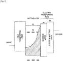
- Fig. 11 shows one example of an organic EL device according to this exemplary embodiment.
- a blue pixel B, a green pixel G and a red pixel R are arranged in parallel on a common substrate 100.
- the blue pixel B includes the anode 10, the hole transporting zone 60, a blue emitting layer 20B, the blocking layer 32, the electron injecting layer 40, the cathode 50, and a protection layer 90 on the substrate 100 in sequential order.
- the green pixel G includes the anode 10, the hole transporting zone 60, a green emitting layer 20G, the blocking layer 32, the electron injecting layer 40, the cathode 50, and the protection layer 90 on the substrate 100 in sequential order.
- the red pixel R includes the anode 10, the hole transporting zone 60, a red emitting layer 20R, the blocking layer 32, the electron injecting layer 40, the cathode 50, and the protection layer 90 on the substrate 100 in sequential order.
- An insulating film 200 is formed between the anodes of adjacent pixels to keep the insulation between the pixels.
- the electron transporting zone is formed of the blocking layer 32 and the electron injecting layer 40.
- the blocking layer is provided as a common blocking layer for the blue pixel B, the red pixel R and the green pixel G.
- the advantageous effects brought by the blocking layer are outstanding comparing to the luminous efficiency conventionally attained in a blue fluorescent device.
- similar advantageous effects such as confining triplet energies in the emitting layer, can be attained, and improvement in luminous efficiency can also be expected.
- a phosphorescent emitting layer it is possible to attain the advantageous effects of confining triplet energies in the emitting layer, and as a result, diffusion of triplet energies is prevented, thereby contributing to improvement in luminous efficiency of a phosphorescent dopant.
- the hole transporting zone is formed of, for instance, a hole transporting layer, or a combination of a hole transporting layer and a hole injecting layer.
- a common hole transporting zone may be provided or different hole transporting zones may be provided for the blue pixel B, the red pixel R and the green pixel G.
- the hole transporting zones respectively have a configuration suited to the color of emitted light.
- the configuration of the organic layer formed of the emitting layers 20B, G and R and the blocking layer is not limited to that shown in the figure and is changeable appropriately.
- the electron transporting zone may not include an electron injecting layer, but a specific compound having an azine ring may serve as an electron injecting layer. Accordingly, in such a case, in the organic EL device 4 shown in Fig. 11 , the electron injecting layer 40 may not be provided on the blocking layer 32 near the cathode 50, so that the blocking layer 32 is adjacent to the cathode 50.
- a green emitting layer is preferably formed of the following host material and dopant material.
- the host material is preferably a fused aromatic ring derivative.
- a fused aromatic ring derivative an anthracene derivative, pyrene derivative and the like are more preferable in view of luminous efficiency and luminous lifetime.
- the host material is exemplified by a heterocycle-containing compound.
- the heterocycle-containing compound are a carbazole derivative, dibenzofuran derivative, ladder-type furan compound and pyrimidine derivative.
- the dopant material is not particularly limited so long as it functions as a dopant, but an aromatic amine derivative is preferable in view of luminous efficiency and the like.
- an aromatic amine derivative a fused aromatic ring derivative having a substituted or unsubstituted arylamino group is preferable. Examples of such a compound are pyrene, anthracene and chrysene having an arylamino group.
- a styrylamine compound is also preferable as the dopant material.
- the styrylamine compound are styrylamine, styryldiamine, styryltriamine and styryltetraamine.
- the styrylamine means a compound in which a substituted or unsubstituted arylamine is substituted with at least one arylvinyl group.
- the arylvinyl group may be substituted with a substituent such as an aryl group, silyl group, alkyl group, cycloalkyl group, or arylamino group, which may have a further substituent.
- a boron complex and a fluoranthene compound are preferable.
- a metal complex is also preferable as the dopant material.
- the metal complex is exemplified by an iridium complex or platinum complex.
- a red emitting layer is preferably formed of the following host material and dopant material.
- the host material is preferably a fused aromatic ring derivative.
- As the fused aromatic ring derivative a naphthacene derivative, pentacene derivative and the like are more preferable in view of luminous efficiency and luminous lifetime.
- the host material is exemplified by a fused polycyclic aromatic compound.
- the fused polycyclic aromatic compound are a naphthalene compound, phenanthrene compound and fluoranthene compound.
- the dopant material is preferably an aromatic amine derivative.
- aromatic amine derivative a fused aromatic ring derivative having a substituted or unsubstituted arylamino group is preferable.
- Such a compound is exemplified by periflanthene having an arylamino group.
- a metal complex is also preferable as the dopant material.
- the metal complex is exemplified by an iridium complex or platinum complex.
- the organic EL device of the fourth exemplary embodiment is prepared in the following manner.
- an APC (Ag-Pd-Cu) layer as a silver alloy layer (reflective layer) and a transparent conductive layer such as a zinc oxide (IZO) film and a tin oxide film are sequentially formed.
- this conductive material layer is patterned by etching using a mask with a resist pattern, thereby forming an anode.
- an insulating film formed of a photosensitive resin such as a polyimide is formed by coating on the anode. Thereafter, the resulting film is exposed, developed and cured to allow the anode to be exposed, whereby the anodes for a blue emitting region, a green emitting region and a red emitting region are patterned.
- Electrodes There are three types of electrodes, i.e. an electrode for the red pixel, an electrode for the green pixel and an electrode for a blue pixel. They respectively correspond to the blue emitting region, the green emitting region and the red emitting region, and respectively correspond to the anode. After conducting cleaning for 5 minutes in isopropyl alcohol, a UV ozone cleaning is conducted for 30 minutes. When the hole injecting layer and the hole transporting layer are formed thereafter, the hole injecting layer is stacked over the entire surface of the substrate, and the hole transporting layer is stacked thereon.
- Emitting layers are formed to be correspondingly arranged to the positions of the anode for the red pixel, the anode for the green pixel and the anode for the blue pixel
- the blue emitting layer, the green emitting layer and the red emitting layer are finely patterned using a shadow mask.
- a blocking layer is stacked over the entire surface.
- an electron injecting layer is stacked over the entire surface.
- Mg and Ag are formed into a film by evaporation, thereby forming a semi-transparent cathode formed of an Mg-Ag alloy.
- the hole transporting layer include an aromatic amine derivative represented by any one of the following formulae (a-1) to (a-5).
- Examples of the substituent that may is contained in Ar 1 to Ar 24 and L 1 to L 9 include a linear or branched alkyl group having 1 to 15 carbon atoms, cycloalkyl group having 3 to 15 ring carbon atoms, trialkylsilyl group having a linear or branched alkyl group having 1 to 15 carbon atoms, triarylsilyl group having an aryl group having 6 to 14 ring carbon atoms, alkylarylsilyl group having a linear or branched alkyl group having 1 to 15 carbon atoms and an aryl group having 6 to 14 ring carbon atoms, aryl group having 6 to 50 ring carbon atoms, heteroaryl group having 5 to 50 ring atoms, halogen atom, and cyano group. Adjacent substituents may bond to each other to form a saturated or unsaturated divalent group forming a ring.
- At least one of the above Ar 1 to Ar 24 is preferably a substituent represented by the following formula (a-6) or (a-7).
- the compound represented by the formula (a-1) is preferably a compound represented by the following formula (a-8).
- the compound represented by the formula (a-8) is preferably a compound represented by the following formula (a-9).
- the compound represented by the formula (a-9) is preferably a compound represented by the following formula (a-10).
- the sample for phosphorescence measurement was put into a quartz cell, cooled to 77(K) and irradiated with exciting light, so that phosphorescence intensity was measured while changing a wavelength.
- the phosphorescence spectrum was expressed in coordinates of which ordinate axis indicated the phosphorescence intensity and of which abscissa axis indicated the wavelength.
- a tangent was drawn to the rise of the phosphorescence spectrum on the short-wavelength side, and a wavelength value L ph (nm) at an intersection of the tangent and the abscissa axis was obtained.
- the tangent to the rise of the phosphorescence spectrum on the short-wavelength side is drawn as follows. While moving on a curve of the phosphorescence spectrum from the short-wavelength side to the maximum spectral value closest to the short-wavelength side among the maximum spectral values, a tangent is checked at each point on the curve toward the long-wavelength of the phosphorescence spectrum. An inclination of the tangent is increased as the curve rises (i.e., a value of the ordinate axis is increased). A tangent drawn at a point of the maximum inclination is defined as the tangent to the rise of the phosphorescence spectrum on the short-wavelength side.
- the maximum with peak intensity being 10% or less of the maximum peak intensity of the spectrum is not included in the above-mentioned maximum closest to the short-wavelength side of the spectrum.
- the tangent drawn at a point of the maximum spectral value being closest to the short-wavelength side and having the maximum inclination is defined as a tangent to the rise of the phosphorescence spectrum on the short-wavelength side.
- Fig. 12 shows an example of a phosphorescent spectrum measured in TB-21.
- a wavelength value L ph (nm) at an intersection of a tangent and the abscissa axis was 447 nm, the tangent being drawn to the rise of the phosphorescent spectrum of TB-21 on the short wavelength side.
- V represents magnitude of the DC voltage
- d represents a total film thickness of the blocking layer material, the electron injecting material and LiF in an electron-only device
- t IS represents a response time T measured by the impedance spectroscopy.
- a single layer of each layer for forming the organic EL device was prepared on a glass substrate by vacuum vapor deposition.
- Ionization potential was measured using the thin film on the glass substrate and a photoelectron spectroscopy (AC-3, manufactured by Riken Keiki Co., Ltd.) under atmosphere. Specifically, a material was irradiated with light and then the amount of electrons generated by charge separation was measured to measure the ionization potential. The square root of photoelectrons ejected in response to energy of irradiation light was plotted. A threshold of photoelectron ejection energy was defined as ionization potential (Ip).
- the energy gap Eg was measured based on an absorption edge of an absorption spectrum in a toluene solution. Specifically, an absorption spectrum was measured with a commercially available ultraviolet-visible spectrophotometer. The energy gap was calculated from a wavelength of the fall of the spectrum on the long-wavelength side.
- L ab means a wavelength value at an intersection of a tangent and the abscissa axis, the tangent being drawn to the fall of the absorption spectrum on the long-wavelength side. unit: nm
- Each compound was dissolved in a toluene solvent (a sample of 2*10 -5 mol/liter) to prepare a sample of 1 cm optical path length. Absorbance was measured while changing a wavelength.
- the maximum absorbance of 0.2 or less is not included in the above-mentioned maximum absorbance on the long-wavelength side.
- Figs. 13 to 15 show examples of an absorption spectrum measured in TB-21, TB-22 and TB-23.
- wavelength values L ab (nm) at an intersection of respective tangents and the abscissa axis, the tangent being drawn to the fall of respective absorption spectra on the long-wavelength side were respectively 417 nm for TB-21, 359 nm for TB-22, and 402 nm for TB-23.
- the ratio of luminous intensity derived from TTF relative to the entire emission can be high, so that a fluorescent device can be highly efficient to the level unachievable by a typically known fluorescent device.
- the ratio of luminous intensity derived from TTF is measurable by a transitional EL method.
- the transitional EL method is a method for measuring reduction behavior (transitional property) of EL emission after DC voltage applied on the device is removed.
- EL luminous intensity are classified into a luminescence component from singlet excitons generated in first recombination and a luminescence component from singlet excitons generated through TTF phenomenon. Since lifetime of the singlet excitons is very short at nano-second order, EL emission is rapidly reduced after removal of DC voltage.
- the TTF phenomenon provides emission from singlet excitons generated through long-life triplet excitons, EL emission is gradually reduced.
- luminous intensity derived from TTF is obtainable.
- the luminous intensity can be determined by the following method.
- Transitional EL waveform is measured as follows (see Fig. 16 ). Pulse voltage waveform output from a voltage pulse generator (PG) is applied on an EL device. The applied voltage waveform is loaded in an oscilloscope (OSC). When a pulse voltage is applied on the EL device, the EL device generates pulse emission. This emission is loaded in the oscilloscope (OSC) through a photomultiplier (PMT). The voltage waveform and the pulse emission are synchronized and loaded in a personal computer (PC).
- OSC oscilloscope
- PMT photomultiplier
- the ratio of luminous intensity is determined as follows based on analysis of the transitional EL waveform.
- a rate equation for reduction behavior of triplet excitons is resolved and the reduction behavior of luminous intensity based on TTF phenomenon is brought into modeling.
- Time-varying reduction of a density n T of triplet excitons within the emitting layer is represented by the following rate equation using a reduction speed v A due to lifetime of the triplet excitons and a reduction speed v C due to collision of the triplet excitons.
- dn T dt ⁇ v A ⁇ n T ⁇ v C ⁇ n T 2
- I TTF represents luminous intensity derived from TTF.
- A is a constant.
- a graph of Fig. 17(A) shows a measurement example where a predetermined DC voltage is applied on the EL device and then the DC voltage is removed and shows time-varying luminous intensity of the EL device.
- the DC voltage was removed at the time of about 3*10 -8 seconds in the graph of Fig. 17A .
- the luminous intensity when voltage is removed is defined as 1. After rapid reduction before the elapse of about 2*10 -7 seconds, a gradual reduction component appears.
- the voltage removal time is a starting point and the reciprocal numbers of the square root of luminous intensity before the elapse of 10 -5 seconds after voltage removal are plotted in an approximately linear line.
- the luminous intensity is preferably fitted in a linear line by the method of least squares.
- the luminous intensity before the elapse of 10 -5 seconds is preferably fitted.
- Fig. 18 exemplarily shows measurement of a TTF ratio of an organic EL device in the following Example 21 in which TB-20 is used as a blocking layer.
- the voltage removal time is a starting point and the reciprocal numbers of the square root of luminous intensity before the elapse of 10 -5 seconds after voltage removal are plotted.
- a glass substrate (size: 25 mm * 75 mm * 1.1 mm thick, manufactured by Geomatec Co., Ltd.) having an ITO transparent electrode (anode) was ultrasonic-cleaned in isopropyl alcohol for five minutes, and then UV/ozone-cleaned for 30 minutes.
- the glass substrate having the transparent electrode line was cleaned, the glass substrate was mounted on a substrate holder of a vacuum evaporation apparatus. Initially, a compound HT-1 was evaporated on a surface of the glass substrate where the transparent electrode line was provided in a manner to cover the transparent electrode, thereby forming a 50 nm thick film of the compound HT-1.
- the HT-1 film serves as a hole injecting layer.
- a compound HT-2 was deposited on the HT-1 film to form an 45 nm thick HT-2 film.
- the HT-2 film serves as a hole transporting layer.
- a compound BH-1 (host material) and a compound BD-1 (dopant material) (mass ratio of BH-1 to BD-1 was 20: 1) were co-evaporated on the HT-2 film to form a 25 nm thick emitting layer.
- TB-10 was deposited on this emitting layer to form a 5 nm thick blocking layer.
- ET-2 electron transporting material
- LiF was deposited on the electron injecting layer to form a 1 nm thick LiF film.
- a metal Al was deposited on the LiF film to form a 150 nm thick metal cathode.
- the organic EL devices were prepared in the same manner as in the Example 1.
- Voltage was applied on the organic EL devices such that a current density was 1 mA/cm 2 , where a value (V) of the voltage was measured.
- EL emission spectrum at that time was measured with a spectral radiance meter (CS-1000, manufactured by KONICA MINOLTA).
- Chromaticity CIE x , CIE y , current efficiency L/J (cd/A), external quantum efficiency EQE (%), and main peak wavelength Lp (nm) were calculated from the obtained spectral-radiance spectrum.
- the organic EL devices of Examples 1 to 3 When TB-10 and TB-11 (compounds having an azine ring in the blocking layer) were used, the organic EL devices of Examples 1 to 3 each exhibited a high external quantum efficiency.
- the reason that the organic EL devices of Examples 1 to 3 exhibited a high external quantum efficiency is considered that the compounds having an azine ring are unlikely to vulnerable to the affinity difference even when the affinity difference existed between the blocking layer and the electron injecting layer, so that the amount of the electrons supplied to the emitting layer is hardly decreased.
- An organic EL device of Example 4 was prepared as follows.
- a glass substrate (size: 25 mm * 75 mm * 1.1 mm thick, manufactured by Geomatec Co., Ltd.) having an ITO transparent electrode (anode) was ultrasonic-cleaned in isopropyl alcohol for five minutes, and then UV/ozone-cleaned for 30 minutes.
- the glass substrate having the transparent electrode line was cleaned, the glass substrate was mounted on a substrate holder of a vacuum evaporation apparatus. Initially, a compound HT-3 was evaporated on a surface of the glass substrate where the transparent electrode line was provided in a manner to cover the transparent electrode, thereby forming a 5 nm thick film of the compound HT-3.
- the HT-3 film serves as a hole injecting layer.
- a compound HT-4 was deposited on the HT-3 film to form a 130 nm thick HT-4 film.
- the HT-4 film serves as a hole transporting layer.
- a compound BH-2 (host material) and a compound BD-1 (dopant material) (mass ratio of BH-2 to BD-1 was 30: 1) were co-evaporated on the HT-4 film to form a 30 nm thick emitting layer. Triplet energy of the compound BH-2 was measured to be 1.83 eV.
- the above compound TB-10 and Liq ((8-quinolinolato)lithium) (donor metal complex) (mass ratio of TB-10 to Liq was1:1) were co-evaporated on the emitting layer to form a blocking layer and an electron injecting layer of 20 nm thickness in total.
- a material for forming the electron injecting layer was the same as that for forming the blocking layer.
- a metal Al was deposited on a film of the blocking layer to form an 80 nm thick metal cathode.
- an organic EL device of Example 4 was prepared.
- the electron transporting zone is substantially provided by the blocking layer that is adjacent to the metal cathode.
- An organic EL device of Example 5 was prepared in the same manner as that of Example 4 except that the compound TB-10, which was one of the materials for forming the blocking layer and the electron injecting layer of the organic EL device of Example 4, was replaced by a compound TB-11.
- the blocking layer and the electron injecting layer in the organic EL device of Example 5 were a co-evaporation layer of the compound TB-11 and Liq.
- the electron transporting zone is substantially provided by the blocking layer that is adjacent to the metal cathode.
- Voltage was applied on the organic EL devices such that a current density was 1 mA/cm 2 , where a value (V) of the voltage was measured.
- EL emission spectrum at that time was measured with a spectral radiance meter (CS-1000, manufactured by KONICA MINOLTA).
- Chromaticity CIE x , CIE y , current efficiency L/J (cd/A), external quantum efficiency EQE (%), and main peak wavelength Lp (nm) were calculated from the obtained spectral-radiance spectrum.
- Voltage pulse waveform (pulse width: 500 micro second, frequency: 20 Hz, voltage: equivalent to 0.1 to 100 mA/cm 2 ) output from a pulse generator (8114A HighSpeed Generator: manufactured by Agilent Technologies) was applied.
- EL emission was input in a photomultiplier (R928: manufactured by Hamamatsu Photonics K.K.).
- the pulse voltage waveform and the EL emission were synchronized and loaded in an oscilloscope (2440: manufactured by Tektronix) to obtain a transitional EL waveform.
- the transitional EL waveform was analyzed to determine a TTF ratio.
- ITO (130 nm) / HT-3 (5 nm) / HT-5 (35 nm) / RH-1 : RD-1 (5 nm, 1 mass%) / HT-6 (3.5 nm) / BH-3 : BD-2 (7 nm, 5 mass%) BH-3 : GD-1 (13 nm, 10 mass%) / blocking layer (X nm) / ET-2 (Y nm) / LiF (1 nm) / Al (80 nm)
- the numerals in parentheses represent a film thickness, and a content ratio of the dopant material (mass%) for the emitting layer including a plurality of components.
- X and Y represent a film thickness and are changed to a value shown in the following Table 4 in each Example.
- organic EL devices of Examples 6 to 11 were prepared as follows.
- a glass substrate (size: 25 mm * 75 mm * 1.1 mm thick, manufactured by Geomatec Co., Ltd.) having an ITO transparent electrode (anode) was ultrasonic-cleaned in isopropyl alcohol for five minutes, and then UV/ozone-cleaned for 30 minutes.
- the glass substrate having the transparent electrode line was cleaned, the glass substrate was mounted on a substrate holder of a vacuum evaporation apparatus. Initially, the following compound HT-3 was evaporated on a surface of the glass substrate where the transparent electrode line was provided in a manner to cover the transparent electrode, thereby forming a 5 nm thick film of the compound HT-3.
- the HT-3 film serves as a hole injecting layer.
- a compound HT-5 was deposited on the HT-3 film to form a 35 nm thick HT-5 film.
- the HT-5 film serves as a hole transporting layer.
- a compound RH-1 (host material) and a compound RD-1 (dopant material) were co-evaporated on the HT-5 film to form a 5 nm thick red emitting layer.
- the concentration of the dopant was 1 mass %.
- HT-6 was deposited on the red emitting layer to form a HT-6 film of 3.5 nm thickness.
- the HT-6 film serves as a charge blocking layer.
- a compound BH-3 (host material) and a compound BD-2 (dopant material) were co-evaporated on the HT-6 film to form a 7 nm thick blue emitting layer.
- the concentration of the dopant was 5 mass %.
- a compound BH-3 (host material) and a compound GD-1 (dopant material) were co-evaporated on the blue emitting layer to form a 13 nm thick green emitting layer.
- the concentration of the dopant was 10 mass %.
- a blocking layer of X nm film thickness was formed on the green emitting layer. Refer to Table 5 regarding a compound for the blocking layer and the film thickness X thereof.
- a compound ET-2 was deposited on the blocking layer to form an ET-2 film of Y nm thickness.
- the ET-2 film serves as an electron injecting layer. Refer to Table 5 regarding a film thickness Y.
- LiF was deposited on the ET-2 film to form a 1 nm thick LiF film.
- a metal Al was deposited on the LiF film to form an 80 nm thick metal cathode.
- Luminous intensity L (cd/m 2 ), chromaticity CIE x , CIE y , current efficiency L/J (cd/A), power efficiency L/P (lm/W) and external quantum efficiency EQE (%) were calculated from the obtained spectral-radiance spectra.
- ITO 130 nm
- HT-3 5 nm
- HT-5 80 nm
- HT-7 15 nm
- BH-1 BH-1
- BD-2 25 nm, 5 mass%)
- blocking layer(20 nm) / ET-2 5 nm
- LiF 1 nm
- Al 80 nm
- the numerals in parentheses represent a film thickness, and a content ratio of the dopant material (mass%) for the emitting layer including a plurality of components.
- a material for the blocking layer was changed to the materials shown in the following Table 5 in each Example.
- an organic EL device of Example 12 was prepared as follows.
- a glass substrate (size: 25 mm * 75 mm * 0.7mm thick, manufactured by Geomatec Co., Ltd.) having an ITO transparent electrode (anode) was ultrasonic-cleaned in isopropyl alcohol for five minutes, and then UV/ozone-cleaned for 30 minutes.
- the glass substrate having the transparent electrode line was cleaned, the glass substrate was mounted on a substrate holder of a vacuum evaporation apparatus. Initially, the following compound HT-3 was evaporated on a surface of the glass substrate where the transparent electrode line was provided in a manner to cover the transparent electrode, thereby forming a 5 nm thick film of the compound HT-3.
- the HT-3 film serves as a hole injecting layer.
- a compound HT-5 was deposited on the HT-3 film to form an 80 nm thick HT-5 film.
- the HT-5 film serves as the first hole transporting layer.
- the compound HT-7 was deposited on the HT-5 film to form a 15 nm thick HT-7 film.
- the HT-7 film serves as a second hole transporting layer.
- a compound BH-1 (host material) and a compound BD-2 (dopant material) (mass ratio of BH-1 to BD-2 was 20: 1) were co-evaporated on the HT-7 film to form a 25 nm thick emitting layer.
- TB-12 was deposited on this emitting layer to form a 20 nm thick blocking layer.
- ET-2 electron transporting material
- LiF was deposited on the electron injecting layer to form a 1 nm thick LiF film.
- a metal Al was deposited on the LiF film to form an 80 nm thick metal cathode.
- ITO (130 nm) / HT-3 (5 nm) / HT-5 (80 nm) / HT-7 (15 nm) / BH-1 : BD-2 (25 nm, 5 mass%) / blocking layer (20 nm) / TB-9 (5 nm) / LiF (1 nm) / Al (80 nm)
- the numerals in parentheses represent a film thickness, and a content ratio of the dopant material (mass%) for the emitting layer including a plurality of components.
- a material for the blocking layer was changed to the materials shown in the following Table 6 in each Example.
- an organic EL device of Example 22 was prepared as follows.
- a glass substrate (size: 25 mm * 75 mm * 0.7mm thick, manufactured by Geomatec Co., Ltd.) having an ITO transparent electrode (anode) was ultrasonic-cleaned in isopropyl alcohol for five minutes, and then UV/ozone-cleaned for 30 minutes.
- the glass substrate having the transparent electrode line was cleaned, the glass substrate was mounted on a substrate holder of a vacuum evaporation apparatus. Initially, the following compound HT-3 was evaporated on a surface of the glass substrate where the transparent electrode line was provided in a manner to cover the transparent electrode, thereby forming a 5 nm thick film of the compound HT-3.
- the HT-3 film serves as a hole injecting layer.
- a compound HT-5 was deposited on the HT-3 film to form an 80 nm thick HT-5 film.
- the HT-5 film serves as the first hole transporting layer.
- the compound HT-7 was deposited on the HT-5 film to form a 15 nm thick HT-7 film.
- the HT-7 film serves as the second hole transporting layer.
- a compound BH-1 (host material) and a compound BD-2 (dopant material) (mass ratio of BH-1 to BD-2 was 20: 1) were co-evaporated on the HT-7 film to form a 25 nm thick emitting layer.
- TB-13 was deposited on this emitting layer to form a 5 nm thick blocking layer.
- TB-9 electron transporting material
- LiF was deposited on the electron injecting layer to form a 1 nm thick LiF film.
- a metal Al was deposited on the LiF film to form an 80 nm thick metal cathode.
- Luminous intensity L (cd/m 2 ), chromaticity CIE x , CIE y , current efficiency L/J (cd/A), power efficiency L/P (lm/W) and external quantum efficiency EQE (%) were calculated from the obtained spectral-radiance spectra.
- a peak wavelength Lp (nm) of the EL emission spectra was also measured.
- ITO (130 nm) / HT-3 (5 nm) / HT-5 (80 nm) / HT-9 (15 nm) / BH-1 : BD-2 (25 nm, 5 mass%) / blocking layer (5 nm) / ET-2 (20 nm) / LiF (1 nm) / Al (80 nm)
- the numerals in parentheses represent a film thickness, and a content ratio of the dopant material (mass%) for the emitting layer including a plurality of components.
- a material for the blocking layer was changed to the materials shown in the following Table 7 in each Example.
- an organic EL device of Example 25 was prepared as follows.
- a glass substrate (size: 25 mm * 75 mm * 0.7mm thick, manufactured by Geomatec Co., Ltd.) having an ITO transparent electrode (anode) was ultrasonic-cleaned in isopropyl alcohol for five minutes, and then UV/ozone-cleaned for 30 minutes.
- the glass substrate having the transparent electrode line was cleaned, the glass substrate was mounted on a substrate holder of a vacuum evaporation apparatus. Initially, the following compound HT-3 was evaporated on a surface of the glass substrate where the transparent electrode line was provided in a manner to cover the transparent electrode, thereby forming a 5 nm thick film of the compound HT-3.
- the HT-3 film serves as a hole injecting layer.
- a compound HT-5 was deposited on the HT-3 film to form an 80 nm thick HT-5 film.
- the HT-5 film serves as the first hole transporting layer.
- the compound HT-9 was deposited on the HT-5 film to form a 15 nm thick HT-9 film.
- the HT-9 film serves as the second hole transporting layer.
- a compound BH-1 (host material) and a compound BD-2 (dopant material) (mass ratio of BH-1 to BD-2 was 20: 1) were co-evaporated on the HT-9 film to form a 25 nm thick emitting layer.
- TB-21 was deposited on this emitting layer to form a 5 nm thick blocking layer.
- ET-2 electron transporting material
- LiF was deposited on the electron injecting layer to form a 1 nm thick LiF film.
- a metal Al was deposited on the LiF film to form an 80 nm thick metal cathode.
- Luminous intensity L (cd/m 2 ), chromaticity CIE x , CIE y , current efficiency L/J (cd/A), power efficiency L/P (lm/W) and external quantum efficiency EQE (%) were calculated from the obtained spectral-radiance spectra.
- a peak wavelength Lp (nm) of the EL emission spectra was also measured.
- the organic EL device of the invention is applicable to a display and an illuminator.
Landscapes
- Physics & Mathematics (AREA)
- Optics & Photonics (AREA)
- Chemical & Material Sciences (AREA)
- Engineering & Computer Science (AREA)
- Materials Engineering (AREA)
- Spectroscopy & Molecular Physics (AREA)
- Electroluminescent Light Sources (AREA)
Claims (12)
- Organische Elektrolumineszenzvorrichtung, die in aufeinanderfolgender Reihenfolge eine Anode, eine Emissionsschicht, eine Elektronentransportzone und eine Kathode umfasst, wobei
die organische Elektrolumineszenzvorrichtung des Weiteren eine Lochtransportzone zwischen der Anode und der Emissionsschicht umfasst,
die Emissionsschicht ein Anthracenderivat als einen Wirt und einen fluoreszierenden Dotierstoff in der Form eines Pyrenderivats umfasst,
eine Sperrschicht an die Emissionsschicht in der Elektronentransportzone angrenzt,
die Sperrschicht ein aromatisches heterocyclisches Derivat umfasst, das durch die unten stehende Formel (1) dargestellt wird: HAr eine substituierte oder unsubstituierte heterocyclische Gruppe darstellt, die 5 bis 30 Ringatome aufweist, und wenn eine Mehrzahl von HAr vorhanden sind, die Mehrzahl von HAr gleich oder verschieden sind;L eine Einfachbindung, einen zweiwertigen oder vierwertigen Rest eines substituierten oder unsubstituierten aromatischen Kohlenwasserstoffrings, der 6 bis 30 Ringkohlenstoffatome aufweist, einen zweiwertigen oder vierwertigen Rest eines substituierten oder unsubstituierten heterocyclischen Rings, der 5 bis 30 Ringatome aufweist, oder einen zweiwertigen oder vierwertigen Rest darstellt, der durch die Kombination in einer Einfachbindung von zwei oder drei Ringen gebildet wird, die aus dem aromatischen Kohlenwasserstoffring und dem heterocyclischen Ring ausgewählt werden;a eine ganze Zahl von 1 bis 3 ist;b eine ganze Zahl von 1 bis 3 ist;Az durch die unten stehende Formel (BL-21-1) dargestellt wird
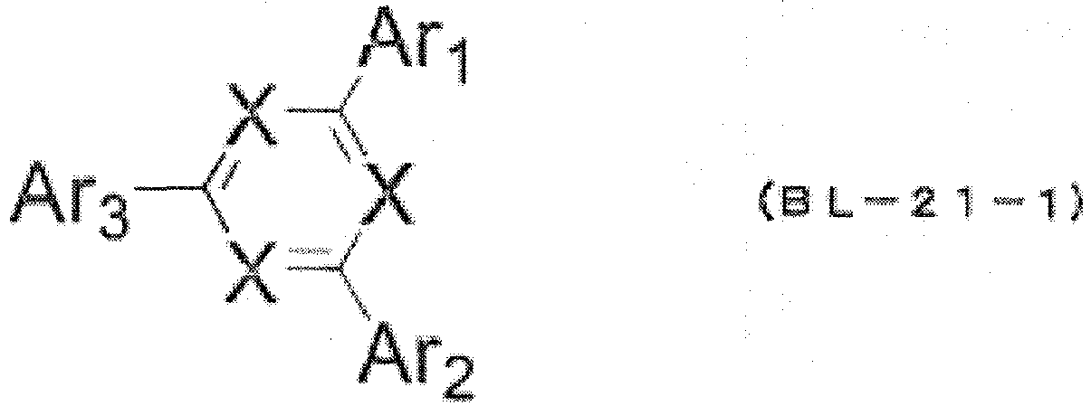 wobei zumindest zwei von drei X N sind, und der Rest von X C(Ar) ist;Ar aus einem Wasserstoffatom, einer substituierten oder unsubstituierten Alkylgruppe, die 1 bis 20 Kohlenstoffatome aufweist, einer substituierten oder unsubstituierten Arylgruppe, die 6 bis 30 Ringkohlenstoffatome aufweist, oder einer substituierten oder unsubstituierten heterocyclischen Gruppe ausgewählt wird, die 5 bis 30 Ringatome aufweist;Ar1, Ar2 and Ar3 jeweils unabhängig voneinander eine Einfachbindung, die in der Formel (1) an L gebunden ist, ein Wasserstoffatom, eine substituierte oder unsubstituierte Alkylgruppe, die 1 bis 20 Kohlenstoffatome aufweist, eine substituierte oder unsubstituierte Arylgruppe, die 6 bis 30 Ringkohlenstoffatome aufweist, oder eine substituierte oder unsubstituierte heterocyclische Gruppe darstellen, die 5 bis 30 Ringatome aufweist;die Triplett-Energie ET b (eV) des aromatischen heterocyclischen Derivats größer als eine Triplett-Energie ET h (eV) des Wirts ist;die Triplett-Energie ET d (eV) des fluoreszierenden Dotierstoffs größer als die Triplett-Energie ET h (eV) des Wirts ist; undeine Lochtransportschicht an die Emissionsschicht in der Lochtransportzone angrenzt, wobei die Lochtransportzone ein aromatisches Aminderivat umfasst, das durch eine der Formeln (a-1) bis (a-5) dargestellt wird;

 Ar1 to Ar24 jeweils unabhängig voneinander eine substituierte oder unsubstituierte Arylgruppe, die 6 bis 50 Ringkohlenstoffatome aufweist, oder eine substituierte oder unsubstituierte Heteroarylgruppe darstellen, die 5 bis 50 Ringatome aufweist,L1 to L9 jeweils unabhängig voneinander eine substituierte oder unsubstituierte Arylengruppe, die 6 bis 50 Ringkohlenstoffatome aufweist, oder eine substituierte oder unsubstituierte Heteroarylengruppe darstellen, die 5 bis 50 Ringatome aufweist,Ar1 bis Ar24 und L1 bis L9 jeweils optional einen Substituenten umfassen, der aus einer linearen oder verzweigten Alkylgruppe, die 1 bis 15 Kohlenstoffatome aufweist, einer Cycloalkylgruppe, die 3 bis 15 Ringkohlenstoffatome aufweist, einer Trialkylsilylgruppe, die eine lineare oder verzweigte Alkylgruppe aufweist, die 1 bis 15 Kohlenstoffatome aufweist, einer Triarylsilylgruppe, die eine Arylgruppe aufweist, die 6 bis 14 Ringkohlenstoffatome aufweist, einer Alkylarylsilylgruppe, die eine lineare oder verzweigte Alkylgruppe, die 1 bis 15 Kohlenstoffatome aufweist, und eine Arylgruppe aufweist, die 6 bis 14 Ringkohlenstoffatome aufweist, einer Arylgruppe, die 6 bis 50 Ringkohlenstoffatome aufweist, einer Heteroarylgruppe, die 5 bis 50 Ringatome aufweist, einem Halogenatom und einer Cyanogruppe ausgewählt ist;eine Mehrzahl von benachbarten des Substituenten sich optional aneinander binden, um eine gesättigte oder ungesättigte zweiwertige Gruppe zu bilden, die einen Ring bildet.
 - Organische Elektrolumineszenzvorrichtung nach Anspruch 1, wobei die Elektronenbeweglichkeit des aromatischen heterocyclischen Derivats zumindest 10-6 cm2/Vs in einer elektrischen Feldintensität von 0,04 MV/cm to 0,5 MV/cm beträgt.
- Organische Elektrolumineszenzvorrichtung nach Anspruch 1 oder 2, wobei die Triplett-Energie ET b (eV) des aromatischen heterocyclischen Derivats und die Triplett-Energie ET h (eV) des Wirts die Beziehung ET h+0,2<ETb erfüllen.
- Organische Elektrolumineszenzvorrichtung nach einem der Ansprüche 1 bis 3, wobei eine Elektroneninjektionsschicht an die Sperrschicht in der Elektronentransportzone angrenzt.
- Organische Elektrolumineszenzvorrichtung nach Anspruch 4, wobei die Elektroneninjektionsschicht ein Material umfasst, das eine Elektronenbeweglichkeit von zumindest 10-6 cm2/Vs in einer elektrischen Feldintensität von 0,04 MV/cm to 0,5 MV/cm aufweist.
- Organische Elektrolumineszenzvorrichtung nach Anspruch 4 oder 5, wobei die Elektroneninjektionsschicht und die Sperrschicht aus demselben Material gebildet sind.
- Organische Elektrolumineszenzvorrichtung nach Anspruch 4 oder 5, wobei die Elektroneninjektionsschicht und die Sperrschicht aus demselben Material gebildet sind, und die Elektroneninjektionsschicht mit einem Donator dotiert ist.
- Organische Elektrolumineszenzvorrichtung nach einem der Ansprüche 1 bis 7, wobei der fluoreszierende Dotierstoff eine Fluoreszenzemission einer Haupt-Spitzenwellenlänge von kleiner oder gleich 550 nm aufweist.
- Organische Elektrolumineszenzvorrichtung nach einem der Ansprüche 1 bis 8, wobei die Triplett-Energie ET ho (eV) der Lochtransportschicht größer als die Triplett-Energie ET h (eV) des Wirts ist.
- Organische Elektrolumineszenzvorrichtung nach einem der Ansprüche 1 bis 9, wobei der Wirt eine Verbindung ist, die eine Doppelbindung nur in einer cyclischen Struktur umfasst.
- Organische Elektrolumineszenzvorrichtung nach einem der Ansprüche 1 bis 10, wobei der fluoreszierende Dotierstoff eine Verbindung ist, die eine Doppelbindung nur in einer cyclischen Struktur enthält.
- Organische Elektrolumineszenzvorrichtung nach einem der Ansprüche 1 bis 11, wobei der fluoreszierende Dotierstoff eine Fluoreszenz zeigt, deren Haupt-Spitzenwellenlänge 480 nm oder weniger beträgt.
Applications Claiming Priority (3)
| Application Number | Priority Date | Filing Date | Title |
|---|---|---|---|
| JP2010260674 | 2010-11-22 | ||
| JP2011165670 | 2011-07-28 | ||
| PCT/JP2011/006511 WO2012070234A1 (en) | 2010-11-22 | 2011-11-22 | Organic electroluminescence device |
Publications (3)
| Publication Number | Publication Date |
|---|---|
| EP2643866A1 EP2643866A1 (de) | 2013-10-02 |
| EP2643866A4 EP2643866A4 (de) | 2014-11-26 |
| EP2643866B1 true EP2643866B1 (de) | 2019-05-08 |
Family
ID=46145599
Family Applications (2)
| Application Number | Title | Priority Date | Filing Date |
|---|---|---|---|
| EP11808815.2A Active EP2643866B1 (de) | 2010-11-22 | 2011-11-22 | Organische elektrolumineszenzvorrichtung |
| EP11813646.4A Active EP2643867B1 (de) | 2010-11-22 | 2011-11-22 | Organische elektrolumineszenzvorrichtung |
Family Applications After (1)
| Application Number | Title | Priority Date | Filing Date |
|---|---|---|---|
| EP11813646.4A Active EP2643867B1 (de) | 2010-11-22 | 2011-11-22 | Organische elektrolumineszenzvorrichtung |
Country Status (6)
| Country | Link |
|---|---|
| EP (2) | EP2643866B1 (de) |
| JP (2) | JP5405653B1 (de) |
| KR (2) | KR101482362B1 (de) |
| CN (2) | CN102668159B (de) |
| TW (2) | TW201232864A (de) |
| WO (2) | WO2012070233A1 (de) |
Families Citing this family (110)
| Publication number | Priority date | Publication date | Assignee | Title |
|---|---|---|---|---|
| KR101478000B1 (ko) * | 2010-12-21 | 2015-01-05 | 롬엔드하스전자재료코리아유한회사 | 신규한 유기 발광 화합물 및 이를 채용하고 있는 유기 전계 발광 소자 |
| JP6197265B2 (ja) * | 2011-03-28 | 2017-09-20 | 東レ株式会社 | 発光素子材料および発光素子 |
| KR101887003B1 (ko) * | 2011-07-21 | 2018-08-13 | 롬엔드하스전자재료코리아유한회사 | 신규한 유기 발광 화합물 및 이를 채용하고 있는 유기 전계 발광 소자 |
| WO2013012298A1 (en) * | 2011-07-21 | 2013-01-24 | Rohm And Haas Electronic Materials Korea Ltd. | 9h-carbazole compounds and electroluminescent devices involving them |
| JP6129075B2 (ja) * | 2011-08-18 | 2017-05-17 | 出光興産株式会社 | ビスカルバゾール誘導体およびこれを用いた有機エレクトロルミネッセンス素子 |
| JP5692011B2 (ja) * | 2011-11-08 | 2015-04-01 | コニカミノルタ株式会社 | 有機エレクトロルミネッセンス素子材料、有機エレクトロルミネッセンス素子、表示装置、並びに照明装置 |
| KR102025031B1 (ko) * | 2011-11-22 | 2019-11-14 | 이데미쓰 고산 가부시키가이샤 | 방향족 복소고리 유도체, 유기 일렉트로루미네선스 소자용 재료 및 유기 일렉트로루미네선스 소자 |
| TWI564297B (zh) * | 2012-06-18 | 2017-01-01 | Tosoh Corp | ring A compound, a method for producing the same, and an organic electroluminescent device containing the same |
| CN104507927A (zh) * | 2012-06-18 | 2015-04-08 | 东曹株式会社 | 环状吖嗪化合物、其制造方法、及含有其的有机电致发光元件 |
| JP6312960B2 (ja) * | 2012-08-03 | 2018-04-18 | 株式会社半導体エネルギー研究所 | 発光素子、発光装置、電子機器、照明装置及び複素環化合物 |
| JP2015216135A (ja) * | 2012-08-10 | 2015-12-03 | 出光興産株式会社 | 有機エレクトロルミネッセンス素子、および電子機器 |
| KR101497138B1 (ko) * | 2012-08-21 | 2015-02-27 | 제일모직 주식회사 | 유기광전자소자 및 이를 포함하는 표시장치 |
| JP6335428B2 (ja) * | 2012-12-21 | 2018-05-30 | 出光興産株式会社 | 有機エレクトロルミネッセンス素子および電子機器 |
| KR102050484B1 (ko) | 2013-03-04 | 2019-12-02 | 삼성디스플레이 주식회사 | 안트라센 유도체 및 이를 포함하는 유기전계발광소자 |
| CN104037326A (zh) * | 2013-03-06 | 2014-09-10 | 海洋王照明科技股份有限公司 | 一种叠层有机电致发光器件及其制备方法 |
| CN104051659A (zh) * | 2013-03-12 | 2014-09-17 | 海洋王照明科技股份有限公司 | 一种叠层有机电致发光器件及其制备方法 |
| CN104051639A (zh) * | 2013-03-12 | 2014-09-17 | 海洋王照明科技股份有限公司 | 一种有机电致发光器件及其制备方法 |
| KR102107106B1 (ko) | 2013-05-09 | 2020-05-07 | 삼성디스플레이 주식회사 | 스티릴계 화합물 및 이를 포함한 유기 발광 소자 |
| KR102407604B1 (ko) * | 2013-05-16 | 2022-06-13 | 가부시키가이샤 한도오따이 에네루기 켄큐쇼 | 발광 소자, 발광 장치, 전자 기기, 및 조명 장치 |
| EP3010055B1 (de) * | 2013-06-11 | 2021-10-20 | Idemitsu Kosan Co., Ltd | Material für organische elektrolumineszierende elemente, organisches elektrolumineszierendes element damit und elektronische vorrichtung |
| KR102269131B1 (ko) | 2013-07-01 | 2021-06-25 | 삼성디스플레이 주식회사 | 화합물 및 이를 포함한 유기 발광 소자 |
| KR102116496B1 (ko) | 2013-08-26 | 2020-05-29 | 삼성디스플레이 주식회사 | 유기 발광 소자 |
| KR102054342B1 (ko) * | 2013-08-26 | 2019-12-11 | 가부시키가이샤 한도오따이 에네루기 켄큐쇼 | 발광 소자, 발광 장치, 표시 장치, 조명 장치, 및 전자 기기 |
| DE112014007423B4 (de) | 2013-12-02 | 2026-04-16 | Semiconductor Energy Laboratory Co., Ltd. | Licht emittierendes Element und Licht emittierende Vorrichtung |
| US10062850B2 (en) | 2013-12-12 | 2018-08-28 | Samsung Display Co., Ltd. | Amine-based compounds and organic light-emitting devices comprising the same |
| KR101742359B1 (ko) * | 2013-12-27 | 2017-05-31 | 주식회사 두산 | 유기 전계 발광 소자 |
| KR102221106B1 (ko) * | 2014-01-17 | 2021-03-02 | 삼성디스플레이 주식회사 | 유기 발광 소자 |
| KR101670056B1 (ko) | 2014-02-20 | 2016-10-28 | 삼성디스플레이 주식회사 | 유기 발광 소자 |
| WO2015142040A1 (en) | 2014-03-17 | 2015-09-24 | Rohm And Haas Electronic Materials Korea Ltd. | Electron buffering material and organic electroluminescent device |
| KR102411748B1 (ko) | 2014-03-17 | 2022-06-23 | 롬엔드하스전자재료코리아유한회사 | 전자 버퍼 재료 및 유기 전계 발광 소자 |
| JP2017123352A (ja) | 2014-03-31 | 2017-07-13 | 出光興産株式会社 | 有機エレクトロルミネッセンス素子および電子機器 |
| KR101537500B1 (ko) * | 2014-04-04 | 2015-07-20 | 주식회사 엘지화학 | 유기 발광 소자 |
| KR102255197B1 (ko) | 2014-05-02 | 2021-05-25 | 삼성디스플레이 주식회사 | 유기 발광 소자 |
| KR102244071B1 (ko) | 2014-05-02 | 2021-04-26 | 삼성디스플레이 주식회사 | 유기 발광 소자 |
| KR102124045B1 (ko) | 2014-05-02 | 2020-06-18 | 삼성디스플레이 주식회사 | 유기 발광 소자 |
| KR102030354B1 (ko) * | 2014-05-13 | 2019-10-10 | 에스에프씨주식회사 | 방향족 아민기를 포함하는 헤테로고리 화합물 및 이를 포함하는 유기 발광 소자 |
| KR20150132795A (ko) | 2014-05-16 | 2015-11-26 | 삼성디스플레이 주식회사 | 유기 발광 소자 |
| KR102283457B1 (ko) * | 2014-06-03 | 2021-07-30 | 삼성디스플레이 주식회사 | 유기 발광 소자 |
| KR102332591B1 (ko) | 2014-06-09 | 2021-11-30 | 삼성디스플레이 주식회사 | 유기 발광 소자 |
| KR102327086B1 (ko) | 2014-06-11 | 2021-11-17 | 삼성디스플레이 주식회사 | 유기 발광 소자 |
| TWI555752B (zh) | 2014-06-27 | 2016-11-01 | 喜星素材股份有限公司 | 雜環化合物及使用其之有機發光裝置 |
| US20170222159A1 (en) * | 2014-07-29 | 2017-08-03 | Rohm And Haas Electronic Materials Korea Ltd. | Electron buffering material and organic electroluminescent device |
| DE112015007286B4 (de) | 2014-08-08 | 2025-11-20 | Semiconductor Energy Laboratory Co., Ltd. | Licht emittierende Vorrichtung |
| KR102526212B1 (ko) | 2014-08-08 | 2023-04-28 | 롬엔드하스전자재료코리아유한회사 | 유기 전계 발광 화합물 및 이를 포함하는 유기 전계 발광 소자 |
| KR102287341B1 (ko) | 2014-08-19 | 2021-08-06 | 삼성디스플레이 주식회사 | 유기 발광 소자 및 이를 포함하는 유기 발광 표시 장치 |
| KR102304720B1 (ko) | 2014-09-19 | 2021-09-27 | 삼성디스플레이 주식회사 | 유기 발광 소자 |
| KR102291896B1 (ko) * | 2014-10-13 | 2021-08-20 | 엘지디스플레이 주식회사 | 전하생성 화합물 및 이를 포함하는 유기전계발광소자 |
| KR101708097B1 (ko) * | 2014-10-22 | 2017-02-17 | 주식회사 두산 | 유기 전계 발광 소자 |
| WO2016068585A1 (ko) * | 2014-10-27 | 2016-05-06 | 주식회사 엘지화학 | 유기 전계 발광 소자 |
| KR102384649B1 (ko) | 2014-11-10 | 2022-04-11 | 삼성디스플레이 주식회사 | 유기 발광 소자 |
| KR102285388B1 (ko) | 2014-11-13 | 2021-08-04 | 삼성디스플레이 주식회사 | 유기 발광 소자 |
| KR102385230B1 (ko) | 2014-11-19 | 2022-04-12 | 삼성디스플레이 주식회사 | 유기 발광 소자 |
| KR102364220B1 (ko) | 2014-12-03 | 2022-02-18 | 삼성디스플레이 주식회사 | 유기 발광 소자 |
| KR102363260B1 (ko) | 2014-12-19 | 2022-02-16 | 삼성디스플레이 주식회사 | 유기 발광 소자 |
| KR102190108B1 (ko) * | 2014-12-31 | 2020-12-11 | 에스에프씨주식회사 | 고효율과 장수명을 갖는 유기 발광 소자 |
| KR102343145B1 (ko) | 2015-01-12 | 2021-12-27 | 삼성디스플레이 주식회사 | 축합환 화합물 및 이를 포함한 유기 발광 소자 |
| KR102201104B1 (ko) * | 2015-01-13 | 2021-01-11 | 에스에프씨주식회사 | 고효율과 장수명을 갖는 유기 발광 소자 |
| EP3248966B1 (de) * | 2015-01-20 | 2022-12-21 | Hodogaya Chemical Co., Ltd. | Pyrimidinderivat und organisches elektrolumineszenzelement |
| TWI723007B (zh) * | 2015-02-18 | 2021-04-01 | 德商諾瓦發光二極體有限公司 | 半導體材料及其萘并呋喃基質化合物 |
| US10903440B2 (en) | 2015-02-24 | 2021-01-26 | Semiconductor Energy Laboratory Co., Ltd. | Light-emitting element, light-emitting device, electronic device, and lighting device |
| KR102338908B1 (ko) | 2015-03-03 | 2021-12-14 | 삼성디스플레이 주식회사 | 유기 발광 소자 |
| KR101847431B1 (ko) | 2015-04-20 | 2018-04-10 | 에스에프씨주식회사 | 유기 발광 소자 |
| CN118530203A (zh) | 2015-04-23 | 2024-08-23 | Sfc株式会社 | 有机发光元件用化合物以及包括该化合物的有机发光元件 |
| US10559758B2 (en) | 2015-07-13 | 2020-02-11 | Sfc Co., Ltd. | Organic light emitting diode of high efficiency |
| KR102002023B1 (ko) | 2015-07-14 | 2019-07-22 | 에스에프씨주식회사 | 고효율의 유기 발광 소자 |
| KR102091695B1 (ko) * | 2015-08-06 | 2020-03-24 | 에스에프씨주식회사 | 고효율을 갖는 유기 발광 소자 |
| KR102500272B1 (ko) | 2015-09-16 | 2023-02-16 | 삼성디스플레이 주식회사 | 화합물 및 이를 포함하는 유기 발광 소자 |
| KR102591635B1 (ko) | 2015-10-27 | 2023-10-20 | 삼성디스플레이 주식회사 | 유기 발광 소자 |
| KR102840102B1 (ko) | 2015-10-30 | 2025-08-01 | 듀폰스페셜티머터리얼스코리아 유한회사 | 전자 버퍼 재료, 전자 전달 재료, 및 이를 포함하는 유기 전계 발광 소자 |
| KR102399570B1 (ko) | 2015-11-26 | 2022-05-19 | 삼성디스플레이 주식회사 | 유기 발광 소자 |
| CN113937228A (zh) | 2015-12-01 | 2022-01-14 | 株式会社半导体能源研究所 | 发光元件、发光装置、电子设备及照明装置 |
| KR102834073B1 (ko) | 2015-12-08 | 2025-07-14 | 이데미쓰 고산 가부시키가이샤 | 유기 el 발광 장치 및 전자 기기 |
| KR102384293B1 (ko) | 2015-12-22 | 2022-04-08 | 삼성디스플레이 주식회사 | 유기 발광 소자 |
| KR102579752B1 (ko) | 2015-12-22 | 2023-09-19 | 삼성디스플레이 주식회사 | 유기 발광 소자 |
| KR20170075122A (ko) | 2015-12-22 | 2017-07-03 | 삼성디스플레이 주식회사 | 유기 발광 소자 |
| KR20170075114A (ko) | 2015-12-22 | 2017-07-03 | 삼성디스플레이 주식회사 | 유기 발광 소자 |
| US11910707B2 (en) | 2015-12-23 | 2024-02-20 | Samsung Display Co., Ltd. | Organic light-emitting device |
| CN105609650A (zh) * | 2015-12-27 | 2016-05-25 | 复旦大学 | 一种基于电荷产生层的在交流电压下驱动的有机发光器件 |
| US11316114B2 (en) | 2016-03-15 | 2022-04-26 | Rohm and Haas Erlectronic Materials Korea Ltd. | Organic electroluminescent compound and organic electroluminescent device comprising the same |
| CN105576146B (zh) | 2016-03-23 | 2017-09-26 | 京东方科技集团股份有限公司 | 发光器件及其制造方法和显示装置 |
| KR20170127101A (ko) | 2016-05-10 | 2017-11-21 | 삼성디스플레이 주식회사 | 유기 발광 소자 |
| JP6804869B2 (ja) * | 2016-05-19 | 2020-12-23 | 出光興産株式会社 | 有機エレクトロルミネッセンス素子用材料、有機エレクトロルミネッセンス素子及び電子機器 |
| KR101958059B1 (ko) * | 2016-07-29 | 2019-03-14 | 엘지디스플레이 주식회사 | 유기 발광 표시 장치 |
| CN106449715A (zh) * | 2016-11-09 | 2017-02-22 | 上海天马有机发光显示技术有限公司 | 一种有机发光显示面板及其制作方法 |
| US10153445B2 (en) * | 2016-11-21 | 2018-12-11 | Universal Display Corporation | Organic electroluminescent materials and devices |
| JPWO2018139662A1 (ja) | 2017-01-30 | 2019-12-26 | 出光興産株式会社 | 有機エレクトロルミネッセンス素子及び電子機器 |
| WO2018151077A1 (ja) * | 2017-02-14 | 2018-08-23 | 出光興産株式会社 | 新規化合物、それを用いた有機エレクトロルミネッセンス素子及び電子機器 |
| KR102008897B1 (ko) | 2017-06-22 | 2019-10-23 | 삼성에스디아이 주식회사 | 유기 광전자 소자 및 표시 장치 |
| KR101947747B1 (ko) | 2018-05-04 | 2019-02-13 | 삼성에스디아이 주식회사 | 유기 광전자 소자용 화합물, 유기 광전자 소자용 조성물, 유기 광전자 소자 및 표시 장치 |
| US20190198772A1 (en) | 2017-06-22 | 2019-06-27 | Samsung Sdi Co., Ltd. | Compound for organic optoelectronic device, composition for organic optoelectronic device and organic optoelectronic device and display deivce |
| KR102162402B1 (ko) | 2017-07-21 | 2020-10-06 | 삼성에스디아이 주식회사 | 유기 광전자 소자 및 표시 장치 |
| KR102401012B1 (ko) * | 2017-07-28 | 2022-05-24 | 삼성디스플레이 주식회사 | 축합환 화합물 및 이를 포함한 유기 발광 소자 |
| KR102497284B1 (ko) * | 2017-12-18 | 2023-02-08 | 삼성디스플레이 주식회사 | 유기 발광 소자 |
| WO2019182360A1 (ko) * | 2018-03-23 | 2019-09-26 | 에스케이머티리얼즈 주식회사 | 화합물, 유기 발광 소자 및 표시 장치 |
| KR102148289B1 (ko) | 2018-07-04 | 2020-08-26 | 에스에프씨주식회사 | 고효율의 유기 발광 소자 |
| KR102794156B1 (ko) | 2019-01-09 | 2025-04-14 | 삼성디스플레이 주식회사 | 유기 전계 발광 소자 및 이를 포함하는 표시 장치 |
| KR20200091979A (ko) * | 2019-01-23 | 2020-08-03 | 삼성디스플레이 주식회사 | 유기 발광 소자 |
| KR102118011B1 (ko) | 2019-03-20 | 2020-06-04 | 에스에프씨주식회사 | 유기 발광 소자용 화합물 및 이를 포함하는 유기발광소자 |
| JP2020188199A (ja) * | 2019-05-16 | 2020-11-19 | 株式会社Joled | 有機el素子、有機el表示パネル、および、有機el素子の製造方法 |
| KR102698882B1 (ko) * | 2019-05-31 | 2024-08-28 | 삼성디스플레이 주식회사 | 유기 발광 소자 및 전자 장치 |
| KR102806405B1 (ko) | 2019-08-16 | 2025-05-14 | 삼성디스플레이 주식회사 | 유기 발광 소자 및 이를 포함한 장치 |
| KR102837684B1 (ko) | 2019-09-11 | 2025-07-23 | 삼성디스플레이 주식회사 | 유기 발광 소자 및 이를 포함한 장치 |
| KR102792637B1 (ko) * | 2019-11-29 | 2025-04-09 | 삼성디스플레이 주식회사 | 유기 전계 발광 소자 및 유기 전계 발광 소자용 아민 화합물 |
| KR102748936B1 (ko) | 2019-12-27 | 2025-01-03 | 삼성디스플레이 주식회사 | 유기 발광 소자 및 이를 포함한 장치 |
| CN113939924B (zh) * | 2020-01-16 | 2024-06-07 | 株式会社Lg化学 | 有机发光器件 |
| KR20230142716A (ko) * | 2021-02-04 | 2023-10-11 | 이데미쓰 고산 가부시키가이샤 | 화합물, 유기 전기발광 소자용 재료, 유기 전기발광소자 및 전자 기기 |
| WO2022209812A1 (ja) * | 2021-03-31 | 2022-10-06 | 出光興産株式会社 | 有機エレクトロルミネッセンス素子、電子機器、及び組成物 |
| US20250324847A1 (en) * | 2022-05-20 | 2025-10-16 | Idemitsu Kosan Co.,Ltd. | Compound, material for organic electroluminescent elements, organic electroluminescent element, and electronic device |
| CN121673300A (zh) * | 2023-12-04 | 2026-03-17 | 安徽省华显新材料科技有限公司 | 一种电子注入材料及oled有机电致发光器件 |
| WO2025142582A1 (ja) * | 2023-12-27 | 2025-07-03 | 出光興産株式会社 | 有機エレクトロルミネッセンス素子及び電子機器 |
Citations (1)
| Publication number | Priority date | Publication date | Assignee | Title |
|---|---|---|---|---|
| KR20070115588A (ko) * | 2006-06-01 | 2007-12-06 | 에스에프씨 주식회사 | 청색발광화합물 및 이를 이용한 유기전계발광소자 |
Family Cites Families (53)
| Publication number | Priority date | Publication date | Assignee | Title |
|---|---|---|---|---|
| JP2940879B2 (ja) | 1990-09-27 | 1999-08-25 | 株式会社ユアサコーポレーション | 鉛蓄電池の開路電圧測定法 |
| JP4208290B2 (ja) | 1998-06-01 | 2009-01-14 | キヤノン株式会社 | 発光素子 |
| US6929870B2 (en) | 2000-08-10 | 2005-08-16 | Mitsui Chemicals, Inc. | Hydrocarbon compounds, materials for organic electroluminescent elements and organic electroluminescent elements |
| TWI267315B (en) | 2002-07-01 | 2006-11-21 | Sony Ericsson Mobile Comm Ab | Communication terminal |
| JP4483167B2 (ja) * | 2002-10-17 | 2010-06-16 | コニカミノルタホールディングス株式会社 | 有機エレクトロルミネッセンス素子および有機エレクトロルミネッセンス素子を有する表示装置 |
| CN1978586A (zh) | 2002-11-12 | 2007-06-13 | 出光兴产株式会社 | 用于有机电致发光器件的材料和使用该材料的有机电致发光器件 |
| EP1437395B2 (de) | 2002-12-24 | 2015-08-26 | LG Display Co., Ltd. | Organische elektrolumineszierende Vorrichtung |
| JP4267623B2 (ja) | 2003-03-20 | 2009-05-27 | 出光興産株式会社 | 芳香族アミン誘導体及びそれを用いた有機エレクトロルミネッセンス素子 |
| KR100527194B1 (ko) * | 2003-06-24 | 2005-11-08 | 삼성에스디아이 주식회사 | 도핑된 정공수송층 및/또는 정공주입층을 갖는유기전계발광소자 |
| JP4799176B2 (ja) * | 2003-07-24 | 2011-10-26 | 株式会社半導体エネルギー研究所 | 発光装置の作製方法 |
| DE10339772B4 (de) | 2003-08-27 | 2006-07-13 | Novaled Gmbh | Licht emittierendes Bauelement und Verfahren zu seiner Herstellung |
| TWI428053B (zh) * | 2004-02-09 | 2014-02-21 | Idemitsu Kosan Co | Organic electroluminescent element |
| TW200541401A (en) * | 2004-02-13 | 2005-12-16 | Idemitsu Kosan Co | Organic electroluminescent device |
| JP4393249B2 (ja) * | 2004-03-31 | 2010-01-06 | 株式会社 日立ディスプレイズ | 有機発光素子,画像表示装置、及びその製造方法 |
| JP4384536B2 (ja) | 2004-04-27 | 2009-12-16 | 三井化学株式会社 | アントラセン化合物、および該アントラセン化合物を含有する有機電界発光素子 |
| KR101192519B1 (ko) | 2004-05-12 | 2012-10-17 | 이데미쓰 고산 가부시키가이샤 | 방향족 아민 유도체, 이를 이용한 유기 전기 발광 소자 및방향족 아민 유도체의 제조방법 |
| TWI373506B (en) | 2004-05-21 | 2012-10-01 | Toray Industries | Light-emitting element material and light-emitting material |
| JP2006049438A (ja) * | 2004-08-02 | 2006-02-16 | Fuji Photo Film Co Ltd | 有機電界発光素子 |
| KR100788254B1 (ko) | 2005-08-16 | 2007-12-27 | (주)그라쎌 | 녹색 발광 화합물 및 이를 발광재료로서 채용하고 있는발광소자 |
| JP4853010B2 (ja) * | 2005-12-15 | 2012-01-11 | コニカミノルタホールディングス株式会社 | 有機エレクトロルミネッセンス素子および有機エレクトロルミネッセンスディスプレイ |
| EP1808909A1 (de) * | 2006-01-11 | 2007-07-18 | Novaled AG | Elekrolumineszente Lichtemissionseinrichtung |
| JP4864476B2 (ja) * | 2006-02-14 | 2012-02-01 | 出光興産株式会社 | 有機エレクトロルミネッセンス素子 |
| US20090021160A1 (en) | 2006-02-23 | 2009-01-22 | Idemitsu Kosan Co., Ltd. | Material for organic electroluminescent device, method for producing same and organic electroluminescent device |
| US7768195B2 (en) * | 2006-05-25 | 2010-08-03 | Idemitsu Kosan Co., Ltd. | Organic electroluminescent device with improved luminous efficiency |
| EP1933397A4 (de) * | 2006-05-25 | 2008-12-17 | Idemitsu Kosan Co | Organische elektrolumineszenzvorrichtung und licht emittierende vorrichtung aller farben |
| CN101473464B (zh) | 2006-06-22 | 2014-04-23 | 出光兴产株式会社 | 应用含有杂环的芳胺衍生物的有机电致发光元件 |
| KR100769884B1 (ko) | 2006-07-14 | 2007-10-30 | 해성쏠라(주) | 투명 크리스탈을 응용한 발광소자 표시장치 |
| US20080049413A1 (en) | 2006-08-22 | 2008-02-28 | Idemitsu Kosan Co., Ltd. | Organic electroluminescence device |
| US8945722B2 (en) * | 2006-10-27 | 2015-02-03 | The University Of Southern California | Materials and architectures for efficient harvesting of singlet and triplet excitons for white light emitting OLEDs |
| KR100874472B1 (ko) | 2007-02-28 | 2008-12-18 | 에스에프씨 주식회사 | 청색발광화합물 및 이를 이용한 유기전계발광소자 |
| JP2008212102A (ja) | 2007-03-07 | 2008-09-18 | Mitsubishi Agricult Mach Co Ltd | コンバイン |
| TW200908777A (en) * | 2007-03-23 | 2009-02-16 | Idemitsu Kosan Co | Organic el device |
| US9353065B2 (en) * | 2007-03-29 | 2016-05-31 | Basf Se | Heterocyclic bridged biphenyls |
| DE102007024850A1 (de) | 2007-05-29 | 2008-12-04 | Merck Patent Gmbh | Neue Materialien für organische Elektrolumineszenzvorrichtungen |
| EP2166589A4 (de) * | 2007-07-07 | 2012-04-04 | Idemitsu Kosan Co | Organische el-vorrichtung |
| JP2009016693A (ja) * | 2007-07-07 | 2009-01-22 | Idemitsu Kosan Co Ltd | ホスト材料および有機el素子 |
| US8294142B2 (en) * | 2007-07-07 | 2012-10-23 | Idemitsu Kosan Co., Ltd. | Organic EL device |
| WO2009011327A1 (ja) | 2007-07-18 | 2009-01-22 | Idemitsu Kosan Co., Ltd. | 有機エレクトロルミネッセンス素子用材料及び有機エレクトロルミネッセンス素子 |
| ATE554073T1 (de) | 2007-11-30 | 2012-05-15 | Idemitsu Kosan Co | Azaindenofluorendionderivat, material für ein organisches elektrolumineszierendes gerät und organisches lumineszierendes gerät |
| JP5355421B2 (ja) | 2007-12-21 | 2013-11-27 | 出光興産株式会社 | 有機エレクトロルミネッセンス素子 |
| WO2009084512A1 (ja) | 2007-12-28 | 2009-07-09 | Idemitsu Kosan Co., Ltd. | 芳香族アミン誘導体及びそれを用いた有機エレクトロルミネッセンス素子 |
| US20090191427A1 (en) * | 2008-01-30 | 2009-07-30 | Liang-Sheng Liao | Phosphorescent oled having double hole-blocking layers |
| WO2009107596A1 (ja) | 2008-02-25 | 2009-09-03 | 出光興産株式会社 | 有機発光媒体及び有機el素子 |
| TWI472074B (zh) * | 2008-03-17 | 2015-02-01 | Nippon Steel & Sumikin Chem Co | Organic electroluminescent elements |
| EP2315290B1 (de) * | 2008-08-04 | 2016-03-16 | Pioneer Corporation | Organisches elektrolumineszenzelement |
| JP5432487B2 (ja) | 2008-08-20 | 2014-03-05 | 出光興産株式会社 | 有機エレクトロルミネッセンス素子 |
| KR101132635B1 (ko) | 2008-08-26 | 2012-04-03 | 에스에프씨 주식회사 | 피렌계 화합물 및 이를 이용한 유기전계발광소자 |
| CN102239140B (zh) | 2008-12-03 | 2014-09-17 | 出光兴产株式会社 | 茚并芴二酮衍生物、有机电致发光元件用材料及有机电致发光元件 |
| JP5279583B2 (ja) * | 2008-12-24 | 2013-09-04 | 出光興産株式会社 | 有機el素子 |
| KR101741415B1 (ko) * | 2009-04-29 | 2017-05-30 | 롬엔드하스전자재료코리아유한회사 | 신규한 유기 발광 화합물 및 이를 채용하고 있는 유기 전계 발광 소자 |
| US20100295445A1 (en) | 2009-05-22 | 2010-11-25 | Idemitsu Kosan Co., Ltd. | Organic electroluminescent device |
| US20100295444A1 (en) * | 2009-05-22 | 2010-11-25 | Idemitsu Kosan Co., Ltd. | Organic electroluminescence device |
| USRE47654E1 (en) * | 2010-01-15 | 2019-10-22 | Idemitsu Koasn Co., Ltd. | Organic electroluminescence device |
-
2011
- 2011-11-22 EP EP11808815.2A patent/EP2643866B1/de active Active
- 2011-11-22 JP JP2012503829A patent/JP5405653B1/ja active Active
- 2011-11-22 CN CN201180003216.8A patent/CN102668159B/zh active Active
- 2011-11-22 KR KR1020127003300A patent/KR101482362B1/ko active Active
- 2011-11-22 WO PCT/JP2011/006510 patent/WO2012070233A1/en not_active Ceased
- 2011-11-22 TW TW100142738A patent/TW201232864A/zh unknown
- 2011-11-22 JP JP2012504990A patent/JP5480364B2/ja active Active
- 2011-11-22 CN CN201180003302.9A patent/CN102668160B/zh active Active
- 2011-11-22 KR KR1020127002764A patent/KR101482829B1/ko active Active
- 2011-11-22 TW TW100142736A patent/TW201301598A/zh unknown
- 2011-11-22 WO PCT/JP2011/006511 patent/WO2012070234A1/en not_active Ceased
- 2011-11-22 EP EP11813646.4A patent/EP2643867B1/de active Active
Patent Citations (1)
| Publication number | Priority date | Publication date | Assignee | Title |
|---|---|---|---|---|
| KR20070115588A (ko) * | 2006-06-01 | 2007-12-06 | 에스에프씨 주식회사 | 청색발광화합물 및 이를 이용한 유기전계발광소자 |
Also Published As
| Publication number | Publication date |
|---|---|
| CN102668160A (zh) | 2012-09-12 |
| KR20120092555A (ko) | 2012-08-21 |
| JP2013543250A (ja) | 2013-11-28 |
| CN102668159A (zh) | 2012-09-12 |
| KR20120092550A (ko) | 2012-08-21 |
| KR101482362B1 (ko) | 2015-01-13 |
| TW201232864A (en) | 2012-08-01 |
| EP2643867B1 (de) | 2019-10-30 |
| JP2014503979A (ja) | 2014-02-13 |
| JP5480364B2 (ja) | 2014-04-23 |
| TW201301598A (zh) | 2013-01-01 |
| WO2012070233A1 (en) | 2012-05-31 |
| CN102668160B (zh) | 2016-06-22 |
| EP2643866A1 (de) | 2013-10-02 |
| EP2643867A1 (de) | 2013-10-02 |
| EP2643866A4 (de) | 2014-11-26 |
| JP5405653B1 (ja) | 2014-02-05 |
| EP2643867A4 (de) | 2014-12-03 |
| KR101482829B1 (ko) | 2015-01-14 |
| CN102668159B (zh) | 2016-08-10 |
| WO2012070234A1 (en) | 2012-05-31 |
Similar Documents
| Publication | Publication Date | Title |
|---|---|---|
| EP2643866B1 (de) | Organische elektrolumineszenzvorrichtung | |
| US9324950B2 (en) | Organic electroluminescence device | |
| EP2434558B1 (de) | Organisches elektrolumineszenzelement | |
| US8883323B2 (en) | Organic electroluminescence device | |
| EP2434559B1 (de) | Organisches elektrolumineszenzelement | |
| US9153790B2 (en) | Organic electroluminescent device | |
| US8476823B2 (en) | Organic electroluminescent device | |
| EP3389107B1 (de) | Organische el-lichtemittierende vorrichtung und elektronisches instrument | |
| EP3211682B1 (de) | Aromatisches heterozyklisches derivat, material für ein organisches elektrolumineszenzelement und organisches elektrolumineszenzelement | |
| US20120126205A1 (en) | Organic electroluminescence device | |
| EP3809482B1 (de) | Organisches elektrolumineszierendes element und material für ein organisches elektrolumineszierendes element | |
| EP2166588A1 (de) | Organische el-vorrichtung | |
| EP2645443A1 (de) | Organisches elektrolumineszenzelement |
Legal Events
| Date | Code | Title | Description |
|---|---|---|---|
| PUAI | Public reference made under article 153(3) epc to a published international application that has entered the european phase |
Free format text: ORIGINAL CODE: 0009012 |
|
| 17P | Request for examination filed |
Effective date: 20120126 |
|
| AK | Designated contracting states |
Kind code of ref document: A1 Designated state(s): AL AT BE BG CH CY CZ DE DK EE ES FI FR GB GR HR HU IE IS IT LI LT LU LV MC MK MT NL NO PL PT RO RS SE SI SK SM TR |
|
| DAX | Request for extension of the european patent (deleted) | ||
| A4 | Supplementary search report drawn up and despatched |
Effective date: 20141027 |
|
| RIC1 | Information provided on ipc code assigned before grant |
Ipc: C09K 11/06 20060101ALI20141021BHEP Ipc: H01L 51/50 20060101AFI20141021BHEP |
|
| STAA | Information on the status of an ep patent application or granted ep patent |
Free format text: STATUS: EXAMINATION IS IN PROGRESS |
|
| 17Q | First examination report despatched |
Effective date: 20170105 |
|
| GRAP | Despatch of communication of intention to grant a patent |
Free format text: ORIGINAL CODE: EPIDOSNIGR1 |
|
| STAA | Information on the status of an ep patent application or granted ep patent |
Free format text: STATUS: GRANT OF PATENT IS INTENDED |
|
| INTG | Intention to grant announced |
Effective date: 20180508 |
|
| GRAS | Grant fee paid |
Free format text: ORIGINAL CODE: EPIDOSNIGR3 |
|
| GRAJ | Information related to disapproval of communication of intention to grant by the applicant or resumption of examination proceedings by the epo deleted |
Free format text: ORIGINAL CODE: EPIDOSDIGR1 |
|
| GRAL | Information related to payment of fee for publishing/printing deleted |
Free format text: ORIGINAL CODE: EPIDOSDIGR3 |
|
| STAA | Information on the status of an ep patent application or granted ep patent |
Free format text: STATUS: EXAMINATION IS IN PROGRESS |
|
| GRAP | Despatch of communication of intention to grant a patent |
Free format text: ORIGINAL CODE: EPIDOSNIGR1 |
|
| STAA | Information on the status of an ep patent application or granted ep patent |
Free format text: STATUS: GRANT OF PATENT IS INTENDED |
|
| INTC | Intention to grant announced (deleted) | ||
| INTG | Intention to grant announced |
Effective date: 20180928 |
|
| GRAJ | Information related to disapproval of communication of intention to grant by the applicant or resumption of examination proceedings by the epo deleted |
Free format text: ORIGINAL CODE: EPIDOSDIGR1 |
|
| GRAL | Information related to payment of fee for publishing/printing deleted |
Free format text: ORIGINAL CODE: EPIDOSDIGR3 |
|
| STAA | Information on the status of an ep patent application or granted ep patent |
Free format text: STATUS: EXAMINATION IS IN PROGRESS |
|
| INTC | Intention to grant announced (deleted) | ||
| GRAR | Information related to intention to grant a patent recorded |
Free format text: ORIGINAL CODE: EPIDOSNIGR71 |
|
| STAA | Information on the status of an ep patent application or granted ep patent |
Free format text: STATUS: GRANT OF PATENT IS INTENDED |
|
| GRAA | (expected) grant |
Free format text: ORIGINAL CODE: 0009210 |
|
| STAA | Information on the status of an ep patent application or granted ep patent |
Free format text: STATUS: THE PATENT HAS BEEN GRANTED |
|
| INTG | Intention to grant announced |
Effective date: 20190325 |
|
| AK | Designated contracting states |
Kind code of ref document: B1 Designated state(s): AL AT BE BG CH CY CZ DE DK EE ES FI FR GB GR HR HU IE IS IT LI LT LU LV MC MK MT NL NO PL PT RO RS SE SI SK SM TR |
|
| REG | Reference to a national code |
Ref country code: GB Ref legal event code: FG4D |
|
| REG | Reference to a national code |
Ref country code: CH Ref legal event code: EP Ref country code: AT Ref legal event code: REF Ref document number: 1131613 Country of ref document: AT Kind code of ref document: T Effective date: 20190515 |
|
| REG | Reference to a national code |
Ref country code: DE Ref legal event code: R096 Ref document number: 602011058838 Country of ref document: DE Ref country code: IE Ref legal event code: FG4D |
|
| REG | Reference to a national code |
Ref country code: NL Ref legal event code: MP Effective date: 20190508 |
|
| REG | Reference to a national code |
Ref country code: LT Ref legal event code: MG4D |
|
| PG25 | Lapsed in a contracting state [announced via postgrant information from national office to epo] |
Ref country code: ES Free format text: LAPSE BECAUSE OF FAILURE TO SUBMIT A TRANSLATION OF THE DESCRIPTION OR TO PAY THE FEE WITHIN THE PRESCRIBED TIME-LIMIT Effective date: 20190508 Ref country code: LT Free format text: LAPSE BECAUSE OF FAILURE TO SUBMIT A TRANSLATION OF THE DESCRIPTION OR TO PAY THE FEE WITHIN THE PRESCRIBED TIME-LIMIT Effective date: 20190508 Ref country code: NL Free format text: LAPSE BECAUSE OF FAILURE TO SUBMIT A TRANSLATION OF THE DESCRIPTION OR TO PAY THE FEE WITHIN THE PRESCRIBED TIME-LIMIT Effective date: 20190508 Ref country code: HR Free format text: LAPSE BECAUSE OF FAILURE TO SUBMIT A TRANSLATION OF THE DESCRIPTION OR TO PAY THE FEE WITHIN THE PRESCRIBED TIME-LIMIT Effective date: 20190508 Ref country code: SE Free format text: LAPSE BECAUSE OF FAILURE TO SUBMIT A TRANSLATION OF THE DESCRIPTION OR TO PAY THE FEE WITHIN THE PRESCRIBED TIME-LIMIT Effective date: 20190508 Ref country code: PT Free format text: LAPSE BECAUSE OF FAILURE TO SUBMIT A TRANSLATION OF THE DESCRIPTION OR TO PAY THE FEE WITHIN THE PRESCRIBED TIME-LIMIT Effective date: 20190908 Ref country code: NO Free format text: LAPSE BECAUSE OF FAILURE TO SUBMIT A TRANSLATION OF THE DESCRIPTION OR TO PAY THE FEE WITHIN THE PRESCRIBED TIME-LIMIT Effective date: 20190808 Ref country code: FI Free format text: LAPSE BECAUSE OF FAILURE TO SUBMIT A TRANSLATION OF THE DESCRIPTION OR TO PAY THE FEE WITHIN THE PRESCRIBED TIME-LIMIT Effective date: 20190508 Ref country code: AL Free format text: LAPSE BECAUSE OF FAILURE TO SUBMIT A TRANSLATION OF THE DESCRIPTION OR TO PAY THE FEE WITHIN THE PRESCRIBED TIME-LIMIT Effective date: 20190508 |
|
| PG25 | Lapsed in a contracting state [announced via postgrant information from national office to epo] |
Ref country code: RS Free format text: LAPSE BECAUSE OF FAILURE TO SUBMIT A TRANSLATION OF THE DESCRIPTION OR TO PAY THE FEE WITHIN THE PRESCRIBED TIME-LIMIT Effective date: 20190508 Ref country code: LV Free format text: LAPSE BECAUSE OF FAILURE TO SUBMIT A TRANSLATION OF THE DESCRIPTION OR TO PAY THE FEE WITHIN THE PRESCRIBED TIME-LIMIT Effective date: 20190508 Ref country code: BG Free format text: LAPSE BECAUSE OF FAILURE TO SUBMIT A TRANSLATION OF THE DESCRIPTION OR TO PAY THE FEE WITHIN THE PRESCRIBED TIME-LIMIT Effective date: 20190808 Ref country code: GR Free format text: LAPSE BECAUSE OF FAILURE TO SUBMIT A TRANSLATION OF THE DESCRIPTION OR TO PAY THE FEE WITHIN THE PRESCRIBED TIME-LIMIT Effective date: 20190809 |
|
| REG | Reference to a national code |
Ref country code: AT Ref legal event code: MK05 Ref document number: 1131613 Country of ref document: AT Kind code of ref document: T Effective date: 20190508 |
|
| PG25 | Lapsed in a contracting state [announced via postgrant information from national office to epo] |
Ref country code: CZ Free format text: LAPSE BECAUSE OF FAILURE TO SUBMIT A TRANSLATION OF THE DESCRIPTION OR TO PAY THE FEE WITHIN THE PRESCRIBED TIME-LIMIT Effective date: 20190508 Ref country code: SK Free format text: LAPSE BECAUSE OF FAILURE TO SUBMIT A TRANSLATION OF THE DESCRIPTION OR TO PAY THE FEE WITHIN THE PRESCRIBED TIME-LIMIT Effective date: 20190508 Ref country code: EE Free format text: LAPSE BECAUSE OF FAILURE TO SUBMIT A TRANSLATION OF THE DESCRIPTION OR TO PAY THE FEE WITHIN THE PRESCRIBED TIME-LIMIT Effective date: 20190508 Ref country code: DK Free format text: LAPSE BECAUSE OF FAILURE TO SUBMIT A TRANSLATION OF THE DESCRIPTION OR TO PAY THE FEE WITHIN THE PRESCRIBED TIME-LIMIT Effective date: 20190508 Ref country code: RO Free format text: LAPSE BECAUSE OF FAILURE TO SUBMIT A TRANSLATION OF THE DESCRIPTION OR TO PAY THE FEE WITHIN THE PRESCRIBED TIME-LIMIT Effective date: 20190508 Ref country code: AT Free format text: LAPSE BECAUSE OF FAILURE TO SUBMIT A TRANSLATION OF THE DESCRIPTION OR TO PAY THE FEE WITHIN THE PRESCRIBED TIME-LIMIT Effective date: 20190508 |
|
| REG | Reference to a national code |
Ref country code: DE Ref legal event code: R097 Ref document number: 602011058838 Country of ref document: DE |
|
| PG25 | Lapsed in a contracting state [announced via postgrant information from national office to epo] |
Ref country code: SM Free format text: LAPSE BECAUSE OF FAILURE TO SUBMIT A TRANSLATION OF THE DESCRIPTION OR TO PAY THE FEE WITHIN THE PRESCRIBED TIME-LIMIT Effective date: 20190508 Ref country code: IT Free format text: LAPSE BECAUSE OF FAILURE TO SUBMIT A TRANSLATION OF THE DESCRIPTION OR TO PAY THE FEE WITHIN THE PRESCRIBED TIME-LIMIT Effective date: 20190508 |
|
| PLBE | No opposition filed within time limit |
Free format text: ORIGINAL CODE: 0009261 |
|
| STAA | Information on the status of an ep patent application or granted ep patent |
Free format text: STATUS: NO OPPOSITION FILED WITHIN TIME LIMIT |
|
| PG25 | Lapsed in a contracting state [announced via postgrant information from national office to epo] |
Ref country code: TR Free format text: LAPSE BECAUSE OF FAILURE TO SUBMIT A TRANSLATION OF THE DESCRIPTION OR TO PAY THE FEE WITHIN THE PRESCRIBED TIME-LIMIT Effective date: 20190508 |
|
| 26N | No opposition filed |
Effective date: 20200211 |
|
| PG25 | Lapsed in a contracting state [announced via postgrant information from national office to epo] |
Ref country code: PL Free format text: LAPSE BECAUSE OF FAILURE TO SUBMIT A TRANSLATION OF THE DESCRIPTION OR TO PAY THE FEE WITHIN THE PRESCRIBED TIME-LIMIT Effective date: 20190508 |
|
| PG25 | Lapsed in a contracting state [announced via postgrant information from national office to epo] |
Ref country code: SI Free format text: LAPSE BECAUSE OF FAILURE TO SUBMIT A TRANSLATION OF THE DESCRIPTION OR TO PAY THE FEE WITHIN THE PRESCRIBED TIME-LIMIT Effective date: 20190508 |
|
| REG | Reference to a national code |
Ref country code: CH Ref legal event code: PL |
|
| PG25 | Lapsed in a contracting state [announced via postgrant information from national office to epo] |
Ref country code: LI Free format text: LAPSE BECAUSE OF NON-PAYMENT OF DUE FEES Effective date: 20191130 Ref country code: CH Free format text: LAPSE BECAUSE OF NON-PAYMENT OF DUE FEES Effective date: 20191130 Ref country code: MC Free format text: LAPSE BECAUSE OF FAILURE TO SUBMIT A TRANSLATION OF THE DESCRIPTION OR TO PAY THE FEE WITHIN THE PRESCRIBED TIME-LIMIT Effective date: 20190508 Ref country code: LU Free format text: LAPSE BECAUSE OF NON-PAYMENT OF DUE FEES Effective date: 20191122 |
|
| REG | Reference to a national code |
Ref country code: BE Ref legal event code: MM Effective date: 20191130 |
|
| PG25 | Lapsed in a contracting state [announced via postgrant information from national office to epo] |
Ref country code: IE Free format text: LAPSE BECAUSE OF NON-PAYMENT OF DUE FEES Effective date: 20191122 |
|
| PG25 | Lapsed in a contracting state [announced via postgrant information from national office to epo] |
Ref country code: BE Free format text: LAPSE BECAUSE OF NON-PAYMENT OF DUE FEES Effective date: 20191130 |
|
| PG25 | Lapsed in a contracting state [announced via postgrant information from national office to epo] |
Ref country code: CY Free format text: LAPSE BECAUSE OF FAILURE TO SUBMIT A TRANSLATION OF THE DESCRIPTION OR TO PAY THE FEE WITHIN THE PRESCRIBED TIME-LIMIT Effective date: 20190508 |
|
| PG25 | Lapsed in a contracting state [announced via postgrant information from national office to epo] |
Ref country code: IS Free format text: LAPSE BECAUSE OF FAILURE TO SUBMIT A TRANSLATION OF THE DESCRIPTION OR TO PAY THE FEE WITHIN THE PRESCRIBED TIME-LIMIT Effective date: 20190908 |
|
| PG25 | Lapsed in a contracting state [announced via postgrant information from national office to epo] |
Ref country code: MT Free format text: LAPSE BECAUSE OF FAILURE TO SUBMIT A TRANSLATION OF THE DESCRIPTION OR TO PAY THE FEE WITHIN THE PRESCRIBED TIME-LIMIT Effective date: 20190508 Ref country code: HU Free format text: LAPSE BECAUSE OF FAILURE TO SUBMIT A TRANSLATION OF THE DESCRIPTION OR TO PAY THE FEE WITHIN THE PRESCRIBED TIME-LIMIT; INVALID AB INITIO Effective date: 20111122 |
|
| PG25 | Lapsed in a contracting state [announced via postgrant information from national office to epo] |
Ref country code: MK Free format text: LAPSE BECAUSE OF FAILURE TO SUBMIT A TRANSLATION OF THE DESCRIPTION OR TO PAY THE FEE WITHIN THE PRESCRIBED TIME-LIMIT Effective date: 20190508 |
|
| REG | Reference to a national code |
Ref country code: DE Ref legal event code: R079 Ref document number: 602011058838 Country of ref document: DE Free format text: PREVIOUS MAIN CLASS: H01L0051500000 Ipc: H10K0050000000 |
|
| P01 | Opt-out of the competence of the unified patent court (upc) registered |
Effective date: 20230522 |
|
| PGFP | Annual fee paid to national office [announced via postgrant information from national office to epo] |
Ref country code: FR Payment date: 20250930 Year of fee payment: 15 |
|
| PGFP | Annual fee paid to national office [announced via postgrant information from national office to epo] |
Ref country code: DE Payment date: 20250930 Year of fee payment: 15 |
|
| PGFP | Annual fee paid to national office [announced via postgrant information from national office to epo] |
Ref country code: GB Payment date: 20251001 Year of fee payment: 15 |