EP2680421B2 - Convertisseur de fréquence doté d'un condensateur de circuit intermédiaire et procédé de pré-charge de celui-ci - Google Patents
Convertisseur de fréquence doté d'un condensateur de circuit intermédiaire et procédé de pré-charge de celui-ci Download PDFInfo
- Publication number
- EP2680421B2 EP2680421B2 EP12174382.7A EP12174382A EP2680421B2 EP 2680421 B2 EP2680421 B2 EP 2680421B2 EP 12174382 A EP12174382 A EP 12174382A EP 2680421 B2 EP2680421 B2 EP 2680421B2
- Authority
- EP
- European Patent Office
- Prior art keywords
- capacitor
- link
- semiconductor switch
- frequency converter
- switch
- Prior art date
- Legal status (The legal status is an assumption and is not a legal conclusion. Google has not performed a legal analysis and makes no representation as to the accuracy of the status listed.)
- Active
Links
Images

Classifications
-
- H—ELECTRICITY
- H02—GENERATION; CONVERSION OR DISTRIBUTION OF ELECTRIC POWER
- H02M—APPARATUS FOR CONVERSION BETWEEN AC AND AC, BETWEEN AC AND DC, OR BETWEEN DC AND DC, AND FOR USE WITH MAINS OR SIMILAR POWER SUPPLY SYSTEMS; CONVERSION OF DC OR AC INPUT POWER INTO SURGE OUTPUT POWER; CONTROL OR REGULATION THEREOF
- H02M5/00—Conversion of AC power input into AC power output, e.g. for change of voltage, for change of frequency, for change of number of phases
- H02M5/40—Conversion of AC power input into AC power output, e.g. for change of voltage, for change of frequency, for change of number of phases with intermediate conversion into DC
- H02M5/42—Conversion of AC power input into AC power output, e.g. for change of voltage, for change of frequency, for change of number of phases with intermediate conversion into DC by static converters
- H02M5/44—Conversion of AC power input into AC power output, e.g. for change of voltage, for change of frequency, for change of number of phases with intermediate conversion into DC by static converters using discharge tubes or semiconductor devices to convert the intermediate DC into AC
- H02M5/453—Conversion of AC power input into AC power output, e.g. for change of voltage, for change of frequency, for change of number of phases with intermediate conversion into DC by static converters using discharge tubes or semiconductor devices to convert the intermediate DC into AC using devices of a triode or transistor type requiring continuous application of a control signal
- H02M5/458—Conversion of AC power input into AC power output, e.g. for change of voltage, for change of frequency, for change of number of phases with intermediate conversion into DC by static converters using discharge tubes or semiconductor devices to convert the intermediate DC into AC using devices of a triode or transistor type requiring continuous application of a control signal using semiconductor devices only
Definitions
- the invention relates to a frequency converter for operating an electrical machine on an electrical network.
- the frequency converter has a supply unit, a converter and a DC link connecting the supply unit to the converter.
- At least one DC link capacitor is provided in the DC intermediate circuit, or DC link for short.
- the invention also relates to a method for charging the DC link capacitor, which is referred to as pre-charging.
- a frequency converter of the type mentioned is from the DE 197 39 553 A1 known.
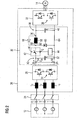
- a frequency converter 10 By means of a frequency converter 10, electrical energy can be exchanged between an AC power supply network, referred to below as network 12 for short, and an electric machine 14.
- the electric machine 14 can be operated as an electric motor or as a generator. Accordingly, the exchange of electrical energy takes place either from the network 12 to the machine 14 or vice versa.
- a network-side feed unit 16 of the frequency converter 10 converts to between the AC mains voltage and a DC voltage U ZK , which is applied between two electrical circuit branches ZK + and ZK- of a DC link 18.
- the circuit branches ZK + and ZK- connect the feed unit 16 with a Inverter 20. They usually include busbars.
- the inverter 20 converts between the DC voltage U ZK and an AC voltage for the electric machine 14.
- the network 12 as shown here, a three-phase network with three network phases R, S, T be. It may be in the network 12 but e.g. also act as a two-phase network. Also, the electric machine 14 may be a machine having any number of phases. Shown here is a three-phase three-phase machine.
- the intermediate circuit 18 provides a DC link capacitor 22 by a sufficiently large capacity for a generated in one of the described conversion steps ripple of the DC voltage U ZK is smoothed so much that it does not affect the other conversion step.
- the DC link capacitor is connected between the two circuit branches ZK +, ZK-.
- the DC link capacitor capacity is also large enough to allow for a brief failure of the AC mains voltage for several milliseconds uninterrupted operation of the electric machine 14.
- the feed unit 16 may be upstream of the line side chokes L 1 , L 2 , L 3 . These prevent interference signals generated by the feed unit 16 during the voltage conversion from being transmitted as harmonics to the network 12.
- the inductors L 1 , L 2 , L 3 can have a further function when the feed unit 16 is operated as a boost converter, which generates a DC voltage U ZK with an effective value which is independent of an effective value of the mains voltage.
- the inductors L 1 , L 2 , L 3 are then designed as Kommut réellesinduktterrorismen that prevent generated in a clocked operation of the feed unit 16 generated short circuits between the individual network phases R, S, T in the feed unit 16 to a commutation with a critical current ,
- the feed unit 16 is electrically connected to the mains phases R, S, T of the network 12 by closing a main contactor 24.
- the supply unit 16 then generates, for example by a full-wave rectification, the DC voltage U ZK , whereby the DC link capacitor 22 is charged. This charging process is referred to below as the precharge phase.
- the electric machine 14 can be operated.
- the converter 20 generates a three-phase AC voltage from the DC voltage U ZK , so that a three-phase current flows in the electric machine 14. This process is referred to below as the operating phase.
- a frequency of the three-phase current may be adjustable in the converter 20.
- the DC link capacitor Before closing the main contactor, the DC link capacitor is usually uncharged. In the precharge phase, this results in the problem that after closing the main contactor, the current strength of the current flowing from the grid in the uncharged DC link capacitor charging current can be so large due to its large capacity that components of the feed unit are damaged.
- the DE 203 11 104 U1 In connection with sporadic voltage jumps at the intermediate circuit side of the feed unit teaches the DE 203 11 104 U1 to couple the feed unit to the DC bus via a common mode choke to prevent the occurrence of overvoltages in the DC bus or in an electrical machine connected to the inverter.
- the inrush current limitation comprises a choke and a freewheeling diode as well as switches by means of which the abovementioned components can be operated as downconverters.
- the Switches where appropriate, the throttle are always arranged in such a way in the switching power supply that they never have to carry the entire input current in normal operation.
- the precharge circuit comprises thyristors as switching elements.
- a frequency converter which has a smoothing circuit parallel to a DC link capacitor for improved rectification of the rectified voltage in the DC link.
- a part of the current flowing through this is passed into this circuit and stored there in a capacitor.
- the capacitor is connected in parallel with a discharge resistor, so that the capacitor discharges continuously and thus can repeatedly absorb another current.
- the circuit comprises a rectifier, a step-up converter and an inverter.
- the rectifier converts a three-phase AC voltage into a rectified voltage.
- the step-up converter generates from the rectified voltage by means of two semiconductor switches, two diodes and a coil according to the "charge-and-pump" principle, a high-voltage for operation the gas discharge lamp. From the high voltage, the inverter generates a two-phase alternating voltage, which is transmitted to electrodes in the gas.
- the frequency converter according to the invention is a development of the generic frequency converter, as in connection with FIG. 1 is explained.
- one of the circuit branch has a throttle.
- One terminal of the choke is connected to a terminal of the DC link capacitor and a second terminal of the choke is connected via a semiconductor switch to a DC link terminal of the supply unit and via a freewheeling diode to the second circuit branch.
- the two connections of the choke are referred to below as corresponding capacitor side and switch side connection.
- the semiconductor switch is designed to control a current intensity of an electric current flowing from the supply unit into the DC link capacitor in dependence on a control signal. Accordingly, to charge the intermediate circuit capacitor in the precharge phase according to the inventive method, first the feed unit is coupled to the network and then the intermediate circuit capacitor is charged with electrical energy from the network. In this case, an average current intensity of an electric current flowing from the feed unit into the DC link capacitor, i. a charging current of the intermediate circuit capacitor, controlled by generating a control signal at a control input of the semiconductor switch by a control device.
- the charging current of the intermediate circuit capacitor in the precharging phase can also be controlled with respect to its current intensity, even when the intermediate circuit capacitor is initially uncharged.
- an average current intensity of the charging current exceeds a critical value, which would lead to destruction of components of the feed unit.
- a temporal change in the current is also limited by the throttle.
- the semiconductor switch it is not necessary for the semiconductor switch to be able to switch particularly quickly, for example, in a pulse-width-modulated switching mode. Thus, 1 kHz to 20 kHz switching frequency may be sufficient. Due to the choke no critical voltage is induced. When the semiconductor switch is opened, the current through the inductor is not interrupted abruptly, as this is instead guided via the semiconductor switch via the freewheeling diode.
- the supply unit can be effectively protected not only during charging of the intermediate circuit capacitor.
- the semiconductor switch may fail in the event of an error, e.g. In the event of a bridge short-circuit in the inverter or in the event of a break-through in the DC link, interrupt a short-circuit current from the network and thus protect the infeed unit against secondary destruction.
- the control device for generating the control signal for the semiconductor switch can be designed in an advantageous manner to generate the control signal as a function of a measured variable, which is dependent on an operating state of the frequency converter. For example, a voltage drop across the intermediate circuit capacitor can be measured and taken into account in the control of its charging current.
- a regulation makes it possible to keep the current flowing through the supply unit always below the critical value even with unknown intermediate capacity or with connected electrical loads (for example a switching power supply for supplying power to a control device of the frequency converter).
- a two-step regulatory procedure for the regulation of the charging current, e.g. a two-step regulatory procedure.
- a clocked, in particular a pulse width modulated signal to the control input of the semiconductor switch be transmitted.
- the semiconductor switch can also be operated as a controllable current source by means of a corresponding control signal.
- a (instantaneous) current intensity of a load current flowing through the semiconductor switch is controlled by adjusting the control signal.
- a load current is to be understood in the case of a bipolar transistor as the collector-emitter current, in the case of a FET as the drain-source current.
- the current intensity of the load current is almost independent of the voltage which drops across the semiconductor switch in the flow direction of the load current.
- the current is instead across the control signal, i. a set control voltage or the set control current, adjustable at the control input (base or gate) of the semiconductor switch.
- this mode of operation corresponds to the operation in the active or amplification range, in the case of a FET the operation in the saturation range.
- the semiconductor switch may comprise a transistor. Since this does not have to switch very fast due to the choke, a low-cost Si transistor, so a transistor based on silicon, can be used.
- the semiconductor switch may also include a SiC-MOSFET (SiC-silicon carbide, MOS-metal-oxide-semiconductor, FET-field-effect-transistor) or a SiC-JFET (JFET-junction-FET). SiC-based transistors are very heat resistant.
- the semiconductor switch is self-locking, ie at a control voltage of 0 V, it is in a blocking state. This prevents in an advantageous manner that in case of failure of the control device for the Semiconductor switch an uncontrolled current flows in the DC link.
- the semiconductor switch does not have to consist of a single component. He can e.g. also comprise a cascode circuit of a MOSFET and a JFET. Then there is the advantage that in the intermediate circuit of the frequency converter, a self-locking semiconductor switch is provided in which a barrier layer of the MOSFET is protected against damage by an overvoltage.
- the JFET is preferably made on the basis of silicon carbide (SiC).
- the throttle may be bridged with a diode in which the passage direction from the inverter to the feed unit is aligned. Then the inductance of the choke has no influence on the current flow in regenerative operation.
- the frequency converter according to the invention additionally has a commutation capacitor in the intermediate circuit, by means of which a commutation capacity for the feed unit is provided.
- the semiconductor switch is in this case connected between the communication capacitor and the intermediate circuit capacitor.
- the commutating capacitor is also electrically connected to the supply unit even when the semiconductor switch is open (blocking).
- the commutation capacity here means a capacity whose value is substantially smaller than the capacitance value of the DC link capacitor is.
- the commutation capacity is preferably less than ten percent, in particular less than one percent, of the DC link capacity.
- An amount of the commutation capacitance may also be selected in dependence on an inductance value of the already described reactors and / or an inductance of the network to which the frequency converter is connected.
- the intermediate circuit capacitor can be charged in several successive charge cycles as follows. In each recharge cycle, the commutating capacitor is first charged with electrical energy from the network when the semiconductor switch is turned off. Subsequently, the energy from the commutation capacitor is transferred to the DC link capacitor by switching the semiconductor switch to a conductive state.
- the semiconductor switch is also designed to selectively interrupt a current flowing from the feed converter to the converter.
- the semiconductor switch is then not only connected upstream of the DC link capacitor itself. Instead, it is interconnected in the DC link so that it can also interrupt the flow of current to the inverter.
- the semiconductor switch is used in addition to switching off the DC link (and the connected converter and an electrical machine) in case of failure. in this connection However, it may come to the induction of an overvoltage through the inductance of the supply network and, where appropriate, the commutation.
- a further commutation capacitor is provided in the intermediate circuit, which can be connected by a switch.
- the switch electrically connects a connection of the further commutation capacitor to the intermediate circuit.
- This further commutation capacitor can then be connected as needed, so that the electrical voltage at the permanently switched commutation capacitor is not too large and damaged this or the semiconductor switch.
- the switch for the further Kommut réelleskondensator can be designed as an electromechanical switch or as an electrical switch.
- the switch can be connected in parallel with an electrical resistance. Then a pre-charging and discharging the other Kommut réelleskondensators with open switch are possible.
- the resistance of the resistor can be used to determine the current intensity of the current.
- At least one discharge resistor can also be connected in parallel with the further commutation capacitor. Then the stored in the further Kommut réelleskondensator after an emergency shutdown electrical energy must not be fed back into the DC link, but can be reduced via the parallel resistor.
- the switch can also be connected in parallel with a diode for discharging the further Kommut istskondensators. Then the discharge rate is higher than when discharging through a resistor.
- a diode connected in series with the switch can prevent a discharge of the further commutation capacitor via the switch, so that the latter is protected against overheating.
- the condenser-side connection of the throttle can likewise be connected via a diode to the further commutation capacitor.
- the diode is current-permeable from the capacitor-side connection to the further commutation capacitor.
- a protection against an overvoltage during an emergency stop can also be effected by means of the semiconductor switch for the intermediate circuit capacitor.
- the semiconductor switch is initially opened for interrupting an operating phase in order to interrupt a current flow from the supply unit to the intermediate circuit capacitor and to the converter. After that, a voltage drop across the commutation capacitor or the semiconductor switch is determined. If this determined voltage is greater in magnitude than a predetermined threshold value, the semiconductor switch is closed again. As a result, electrical charge can flow away from the commutation capacitor into the DC link capacitor, so that the voltage at the commutation capacitor drops.
- the semiconductor switch can be closed several times briefly during the shutdown, e.g. for less than 1 s, in particular less than 100 ms. The closing of the semiconductor switch and the reopening can be done in dependence on the determined voltage.
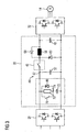
- FIG. 2 a frequency converter 26 is shown, which is connected via a main contactor 24 to phases R, S, T of a network 12. To the frequency converter 26, an electric machine 14 is connected.
- the network 12, the main contactor 24 and the electric machine 14, which in FIG. 2 are shown correspond to the in FIG. 1 shown elements with the same reference numerals. These elements are therefore not explained again here.
- a feed unit 28 is connected via a DC link 30 to a converter 32.
- the feed unit 28 may be configured in a known manner. It has three half-bridges in the example shown for rectifying the alternating voltages applied between the phases R, S, T, of which in FIG. 2 the sake of clarity, only a half-bridge 34 is shown without further interconnection elements.
- the feed unit 28 can also be operated as an inverter for feeding electrical energy into the network 12.
- the inverter 32 may also be configured in a known manner. In the present example, it comprises three half-bridges, of those in FIG. 2 only a half-bridge 36 (without interconnection elements) is shown.
- the inverter 32 can be operated here as an AC and rectifier.
- the supply unit 28 are upstream of the network side chokes L 1 , L 2 , L 3 , which are formed as Kommutêtsinduktditeen.
- An inverter-side part 38 of the intermediate circuit 30 and a supply-side part 40 are interconnected via a switching device 42.
- a control input G of a Si transistor 46 of the switching device 42 is coupled to a control device 44.
- the supply-side part 40 and the converter-side part 38 of the intermediate circuit 30 are coupled to one another via the Si transistor 46.
- the control device 44 controls a volume resistance of the Si transistor 46 by generating a corresponding control voltage at the control input G.
- the Si transistor 46 is here a self-locking component.
- a SiC-MOSFET, a SiC-JFET or a cascode circuit of a MOSFET and a JFET may be used.
- a DC link capacitor 48 In the converter-side part 38 is a DC link capacitor 48.
- a capacity of the DC link capacitor 48 may be greater than 1 mF in the example shown.
- a plurality of capacitors may be provided for providing the DC link inductance.
- busbars of the intermediate circuit are capacitively coupled to one another via a commutation capacitor 52.
- the commutation capacitor 52 may be a ceramic or foil capacitor.
- the capacitance of the commutation capacitor 52 is less than 5 ⁇ F in this example. However, it is generally a function of a via the frequency converter 26 conductive total power chosen, wherein it also preferably less than ten percent of the capacity of the DC link capacitor 48.
- the capacitance value of the DC link capacitor 48 i. the DC link capacitance is so large that closing the main contactor 24 would damage the half bridge 34 (and the remaining half bridges of the feed unit 28) if the charging current of the DC link capacitor 48 were not limited.
- the intermediate circuit capacitor 48 is charged in a precharge phase with a charging current whose current does not exceed a critical value.
- the control unit 44 sets the control voltage at the control input G such that a current intensity of the charging current flowing through the Si transistor 46 of the intermediate circuit capacitor 48 is correspondingly limited.
- the precharging of the intermediate circuit 30 can be performed clocked.
- the Si transistor 46 is first switched to a blocking state, so that the converter-side part 38 of the intermediate circuit 30 is electrically isolated from the feed unit 28.
- the main contactor 24 is closed, so that the feed unit 28 at insectseitgen terminals 54, 56 generates a rectified voltage Uzk.
- the current consumption of the commutation capacitor 52 is limited only by the commutation of the inductors L 1 , L 2 , L 3 . Since the commutation capacitance of the commutation capacitor 52 is relatively small, it is quickly charged to the rectification value of the mains voltage. Thus, despite the hard, ie abrupt, connection of the commutation capacitor 52 to the network 12, the average current strength does not rise above a critical value for the feed unit 28. Since the Si transistor 46 blocks during this process, the DC link capacitor 48 remains uncharged.
- a clocked control signal is generated by the control unit 44 at the control input G, the pulse-pause times as needed and can be selected according to the size of the DC link capacity.
- the Si transistor 46 is switched to a conductive state in pulses or bursts, so that electrical charge is transferred from the commutation capacitor 52 via the Si transistor 46 into the DC link capacitor 48.
- the Si transistor 46 may be continuously turned on, or may be opened several times only for a short time, e.g. with a switching frequency of 1 kHz to 20 kHz.
- the first transfer cycle is terminated by switching the Si transistor 46 permanently back to the blocking state.
- the commutation capacitor 52 is thereby recharged with electrical energy from the network 12 via diodes of the half bridges of the feed unit 28, i. a second transfer cycle is started.
- a free-wheeling diode 60 serves to free-wheel the throttle 58 after each opening of the Si transistor 46.
- the freewheeling diode 60 is connected between two busbar branches 62, 64 of the intermediate circuit 30.
- the free-wheeling diode 60 connects the minus potential busbar branch 64 to a switch-side terminal 66 of the choke 58 in the plus potential busbar branch 62.
- the freewheeling current can be between the intermediate circuit capacitor and the free-wheeling diode flow, since the DC link capacitor and the freewheeling diode are on the one hand connected together on one of the busbar branches and on the other hand are coupled via the throttle.
- the Si transistor 46 can also be operated as a controlled current source for the transfer of electrical energy. For this purpose, it is turned on only in part, so that although it is in a conductive state, but the voltage dropping above it is large enough to limit the load current in the desired manner.
- the control signal for the control input G can have a predetermined course.
- a controlled operation is also possible in which the control signal, e.g. the pulse-pause times of a rectangular signal in the clocked operation, is set in dependence on a measured variable. For example, a charge state of the intermediate circuit capacitor 48 can be determined for this purpose.
- the choke 58 can optionally be bridged by a diode 68, which can connect a capacitor-side terminal 70 of the choke 58 to the switch-side terminal 66.
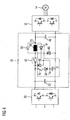
- FIG. 3 and FIG. 4 two advantageous circuit variants of a frequency converter according to the invention are described.
- FIG. 3 and FIG. 4 are elements that function in accordance with elements that are related to FIG. 1 and FIG. 2 have been explained with the same reference numerals as in FIG. 1 respectively.
- FIG. 3 an intermediate circuit 30 is shown, in which a commutation capacitor 72 is provided in parallel to a Kommut réelleskondensator 52 in a feed-side part.
- the further commutation capacitor 72 can be connected as needed.
- a connection 74 of the commutation capacitor 72 is connected to a busbar branch 62 via a switch 76, for example an electromechanical or electrical switch.
- the switch 76 may be connected in parallel with an electrical resistor 78 and / or a discharging diode 80 for the commutating capacitor 72.
- FIG. 4 an intermediate circuit 30 is shown, in which a further switchable via a switch 76 commutation capacitor 72 is also provided. A current flow from the commutation capacitor 72 back to the switch 76 is blocked by a diode 82.
- a charging diode 84 connects a capacitor-side terminal 70 of a choke 58 to a terminal 74 of the commutation capacitor 72, via which the commutation capacitor 72 is also coupled to the switch 76.
- the switch of the switching device 42 is opened in the event of a fault (eg in the case of a DC link short circuit).
- the current from the supply unit 28 then commutates to the commutation capacitor 52. If its capacity is insufficient to absorb the energy stored in the commutation chokes L1 to L3, so that the voltage Uzk on Kommut réelleskondensator 52 exceeds a limit, the switching device 42 can be turned on for a short time be (eg for less as 1 s, in particular less than 100 ms) in order to reduce the voltage Uzk until it falls below a predetermined value, for example the limit value. This is then repeated until the voltage at the commutation capacitor 52 falls below the limit permanently.
- the short-term switching of the switching device 42 in case of failure is uncritical for the half-bridge 34 of the feed device 28 and also for the switching device 42 itself, as long as their maximum short-circuit times are not exceeded.
- the supply-side commutation capacity can be increased by connecting the further commutation capacitor 72.
- a switch e.g. an SI transistor
- the drive circuit of the switching unit 44 can thus be designed significantly less expensive and thus cheaper.
- a cheaper Si transistor 46 may be used instead of a faster switching SiC transistor.
Landscapes
- Engineering & Computer Science (AREA)
- Power Engineering (AREA)
- Inverter Devices (AREA)
- Rectifiers (AREA)
Claims (13)
- Convertisseur (26) de fréquence pour faire fonctionner une machine (14) électrique sur un réseau (12) électrique, dans lequel- le convertisseur (26) de fréquence ayant une unité (28) d'alimentation et un convertisseur (32) qui sont reliés entre eux par un circuit (30) intermédiaire en tension continue, dans lequel sont montées, par un condensateur (48) de circuit intermédiaire, une première et une deuxième branches (62, 64) du circuit (30) intermédiaire,- la première branche (62) du circuit a une bobine de self (58), à laquelle une borne (70) du côté du condensateur est reliée à une borne du condensateur (48) du circuit intermédiaire et une borne (66) du côté commutateur est reliée par un commutateur (42) à semi-conducteur à une borne (54) de circuit intermédiaire de l'unité (28) d'alimentation d'une part et par une diode (60) de roue libre à la deuxième branche (64) du circuit d'autre part,- le commutateur (42) à semi-conducteur étant conçu pour, pendant une phase de pré-charge du condensateur (48) du circuit intermédiaire, commander, en fonction d'un signal de commande, une intensité d'un courant électrique passant de l'unité (28) d'alimentation au condensateur (48) de circuit intermédiaire,- le commutateur (42) à semi-conducteur est conçu et monté dans le circuit (30) intermédiaire, pour interrompre au choix dans le circuit (30) intermédiaire également le flux de courant allant au convertisseur (32),- le circuit (30) intermédiaire a un condensateur (52) de commutation, par lequel il est ménagé une capacité de commutation de l'unité (28) d'alimentation,- le commutateur (42) à semi-conducteur étant monté entre le condensateur (52) de commutation et le condensateur (48) du circuit intermédiaire et- le circuit (30) intermédiaire a un autre condensateur (72) de commutation et un commutateur (76), qui, à l'état fermé, relie électriquement une borne (74) de l'autre condensateur (72) de commutation à l'une des branches (62, 64) du circuit.
- Convertisseur (26) de fréquence suivant la revendication 1, dans lequel le commutateur (42) à semi-conducteur comprend un transistor, notamment un transistor (46) au SI, le commutateur (42) à semi-conducteur étant de préférence à enrichissement.
- Convertisseur (26) de fréquence suivant la revendication 1 ou 2, dans lequel la bobine de self (58) est shuntée par une diode (68), un sens passant de la diode (68) allant du convertisseur (32) à l'unité (28) d'alimentation.
- Convertisseur (26) de fréquence suivant l'une des revendications précédentes, caractérisé en ce qu'une résistance (78) électrique est montée en parallèle au commutateur (76).
- Convertisseur (26) de fréquence suivant l'une des revendications précédentes, caractérisé en ce qu'une diode (80) de décharge de l'autre condensateur (72) de commutation est montée en parallèle au commutateur (76).
- Convertisseur (26) de fréquence suivant l'une des revendications précédentes, dans lequel, dans le commutateur (76), une diode (82), montée en série avec le commutateur (76), bloque par le commutateur (76) une décharge de l'autre condensateur (72) de commutation.
- Convertisseur (26) de fréquence suivant l'une des revendications précédentes, caractérisé en ce que la borne (70) du côté du condensateur de la bobine de self (58) est reliée par une diode (84) à l'autre condensateur (72) de commutation, la diode (84) laissant passer le courant de la borne (70) du côté du condensateur à l'autre condensateur (72) de commutation.
- Convertisseur (26) de fréquence suivant l'une des revendications précédentes, caractérisé en ce qu'au moins une résistance de décharge est montée en parallèle à l'autre condensateur (72) de commutation.
- Procédé pour faire fonctionner un convertisseur (26) de fréquence suivant l'une des revendications précédentes, comprenant les stades :- de couplage de l'unité (28) d'alimentation au réseau (12) ;- dans une phase de pré-charge, de charge du condensateur (48) du circuit intermédiaire en énergie électrique provenant du réseau (12) et de commande ainsi d'une intensité d'un courant de charge passant dans le condensateur (48) du circuit intermédiaire, en produisant un signal de commande sur une entrée (G) de commande du commutateur (42) à semi-conducteur, une modification dans le temps de l'intensité du courant étant limitée par la bobine de self (58) et, à l'ouverture du commutateur (42) à semi-conducteur, le courant de charge passant par la diode (60) de roue libre au lieu de passer par le commutateur (42) à semi-conducteur,- pendant la phase de fonctionnement, d'interruption par le commutateur (42) à semi-conducteur d'un courant de court-circuit provenant du réseau en cas de panne.
- Procédé suivant la revendication 9, dans lequel le signal de commande est produit par un dispositif (44) de commande en fonction d'une grandeur de mesure, qui dépend d'un état de fonctionnement du convertisseur (26) de fréquence, notamment en fonction d'une tension chutant aux bornes du condensateur (48) du circuit intermédiaire, le dispositif (44) de commande régulant l'intensité du courant, notamment au moyen d'un procédé de régulation à deux positions.
- Procédé suivant la revendication 9 ou 10, dans lequel, dans la phase de pré-charge, pour la commande de l'intensité du courant, on transmet à l'entrée (G) de commande, comme signal de commande, un signal cadencé, notamment à impulsions modulées en largeur.
- Procédé suivant l'une des revendications 9 à 11 pour faire fonctionner un convertisseur de fréquence suivant l'une des revendications 4 à 10, dans lequel, dans la phase de pré-charge, pour charger le condensateur (48) du circuit intermédiaire, on fait passer de l'énergie électrique dans des cycles successifs du condensateur (52) de commutation au condensateur (48) de circuit intermédiaire et à cet effet on charge dans chaque cycle, alors que le commutateur (42) à semi-conducteur est bloqué, le condensateur (52) de commutation en énergie électrique provenant du réseau (12) et ensuite, alors que le commutateur (42) à semi-conducteur est passant, on charge le condensateur (48) du circuit intermédiaire en énergie à partir du condensateur (52) de commutation.
- Procédé suivant l'une des revendications 9 à 12 pour faire fonctionner un convertisseur de fréquence suivant l'une des revendications 4 à 8, dans lequel on ouvre le commutateur (42) à semi-conducteur pour interrompre une phase de fonctionnement, afin d'interrompre un flux de courant allant de l'unité (28) d'alimentation au condensateur (48) du circuit intermédiaire et au convertisseur (32), puis on détermine une tension chutant aux bornes du condensateur (52) de commutation ou aux bornes du commutateur (42) à semi-conducteur et on referme le commutateur (42) à semi-conducteur si la tension déterminée est en valeur absolue plus grande qu'une valeur de seuil déterminée à l'avance.
Priority Applications (2)
| Application Number | Priority Date | Filing Date | Title |
|---|---|---|---|
| EP12174382.7A EP2680421B2 (fr) | 2012-06-29 | 2012-06-29 | Convertisseur de fréquence doté d'un condensateur de circuit intermédiaire et procédé de pré-charge de celui-ci |
| US13/930,561 US9318969B2 (en) | 2012-06-29 | 2013-06-28 | Frequency converter with DC link capacitor and method for pre-charging the DC link capacitor |
Applications Claiming Priority (1)
| Application Number | Priority Date | Filing Date | Title |
|---|---|---|---|
| EP12174382.7A EP2680421B2 (fr) | 2012-06-29 | 2012-06-29 | Convertisseur de fréquence doté d'un condensateur de circuit intermédiaire et procédé de pré-charge de celui-ci |
Publications (3)
| Publication Number | Publication Date |
|---|---|
| EP2680421A1 EP2680421A1 (fr) | 2014-01-01 |
| EP2680421B1 EP2680421B1 (fr) | 2015-04-01 |
| EP2680421B2 true EP2680421B2 (fr) | 2018-08-08 |
Family
ID=46583851
Family Applications (1)
| Application Number | Title | Priority Date | Filing Date |
|---|---|---|---|
| EP12174382.7A Active EP2680421B2 (fr) | 2012-06-29 | 2012-06-29 | Convertisseur de fréquence doté d'un condensateur de circuit intermédiaire et procédé de pré-charge de celui-ci |
Country Status (2)
| Country | Link |
|---|---|
| US (1) | US9318969B2 (fr) |
| EP (1) | EP2680421B2 (fr) |
Families Citing this family (30)
| Publication number | Priority date | Publication date | Assignee | Title |
|---|---|---|---|---|
| US9425705B2 (en) * | 2012-08-13 | 2016-08-23 | Rockwell Automation Technologies, Inc. | Method and apparatus for bypassing cascaded H-bridge (CHB) power cells and power sub cell for multilevel inverter |
| US9240731B2 (en) | 2013-03-18 | 2016-01-19 | Rockwell Automation Technologies, Inc. | Power cell bypass method and apparatus for multilevel inverter |
| US9520800B2 (en) | 2014-01-09 | 2016-12-13 | Rockwell Automation Technologies, Inc. | Multilevel converter systems and methods with reduced common mode voltage |
| US9379575B2 (en) * | 2014-03-07 | 2016-06-28 | Nissan North America, Inc. | Battery charger noise reduction by frequency switching |
| ITBA20150014U1 (it) * | 2014-04-02 | 2016-09-02 | Ribawood Sa | Pallet in struttura alleggerita e relativo connettore per traversa-pattino dotato di mezzi di facile estrazione |
| US9559541B2 (en) | 2015-01-15 | 2017-01-31 | Rockwell Automation Technologies, Inc. | Modular multilevel converter and charging circuit therefor |
| DK3068024T3 (en) | 2015-03-09 | 2018-04-23 | Siemens Ag | Procedure for controlling a Vienna rectifier |
| US9748862B2 (en) | 2015-05-13 | 2017-08-29 | Rockwell Automation Technologies, Inc. | Sparse matrix multilevel actively clamped power converter |
| JP6285475B2 (ja) * | 2016-01-29 | 2018-02-28 | ファナック株式会社 | 放電機能を有するモータ駆動装置 |
| EP3217522A1 (fr) | 2016-03-08 | 2017-09-13 | Siemens Aktiengesellschaft | Systeme redresseur ayant une capacite de retour |
| RU2619917C1 (ru) * | 2016-04-25 | 2017-05-19 | Акционерное общество "Конструкторское бюро специального машиностроения" | Устройство гарантированного электропитания |
| US9812990B1 (en) | 2016-09-26 | 2017-11-07 | Rockwell Automation Technologies, Inc. | Spare on demand power cells for modular multilevel power converter |
| EP3379675A1 (fr) | 2017-03-23 | 2018-09-26 | Siemens Aktiengesellschaft | Construction optimisée d'un système de tension continue et procédé lors d'une panne du réseau d'alimentation |
| EP3410592B1 (fr) | 2017-05-30 | 2019-12-25 | ABB Schweiz AG | Cellule de convertisseur à cellule photovoltaïque intégrée |
| EP3490128B2 (fr) | 2017-11-28 | 2025-01-01 | KEB Automation KG | Circuit protection électronique |
| EP3490132A1 (fr) * | 2017-11-28 | 2019-05-29 | Siemens Aktiengesellschaft | Onduleur à circuit intermédiaire doté de l'accouplement ciblé avec au moins un autre onduleur à circuit intermédiaire |
| DE202017007712U1 (de) | 2017-11-28 | 2024-10-28 | Keb Automation Kg | Elektronische Schutzschaltung |
| EP3490129B1 (fr) | 2017-11-28 | 2020-01-08 | KEB Automation KG | Circuit protection électronique |
| DE102017130882A1 (de) * | 2017-12-21 | 2019-06-27 | Sma Solar Technology Ag | Wechselrichter und Betriebsverfahren für einen Wechselrichter |
| US10158299B1 (en) | 2018-04-18 | 2018-12-18 | Rockwell Automation Technologies, Inc. | Common voltage reduction for active front end drives |
| CN110677060B (zh) * | 2018-07-02 | 2021-08-03 | 台达电子工业股份有限公司 | 功率变换系统及其中直流母线电容的预充电方法 |
| DE102018212825A1 (de) * | 2018-08-01 | 2020-02-06 | Schmidhauser Ag | DC/DC-Wandler und Netzrückspeiseeinheit |
| JP6987266B2 (ja) * | 2018-09-12 | 2021-12-22 | 三菱電機株式会社 | 電力変換装置および空気調和機 |
| EP3648324A1 (fr) * | 2018-10-30 | 2020-05-06 | Siemens Aktiengesellschaft | Onduleur de fréquence à pré-commutation simplifiée |
| US10855169B1 (en) | 2019-09-10 | 2020-12-01 | Lear Corporation | Configurable multi-phase charger |
| US11211879B2 (en) | 2019-09-23 | 2021-12-28 | Rockwell Automation Technologies, Inc. | Capacitor size reduction and lifetime extension for cascaded H-bridge drives |
| EP4068602A1 (fr) * | 2021-03-30 | 2022-10-05 | Siemens Aktiengesellschaft | Dispositif condensateur, module d'onduleur pourvu de dispositif condensateur, système d'onduleur pourvu de module d'onduleur et procédé de remplacement pour le système d'onduleur |
| US11342878B1 (en) | 2021-04-09 | 2022-05-24 | Rockwell Automation Technologies, Inc. | Regenerative medium voltage drive (Cascaded H Bridge) with reduced number of sensors |
| EP4178103A1 (fr) * | 2021-11-09 | 2023-05-10 | Hilti Aktiengesellschaft | Outil électrique pouvant être géré par réseau |
| CN118572646B (zh) * | 2024-07-31 | 2024-10-18 | 广东电网有限责任公司珠海供电局 | 直流配电系统多工况自适应致稳控制装置及其控制方法 |
Citations (5)
| Publication number | Priority date | Publication date | Assignee | Title |
|---|---|---|---|---|
| DE10248971A1 (de) † | 2002-10-17 | 2004-05-19 | Demag Cranes & Components Gmbh | Frequenzumrichter für einen drehstrombetriebenen Motor, insbesondere eines Hebezeugs |
| US20070052403A1 (en) † | 2005-08-24 | 2007-03-08 | Micrel, Incorporated | Analog internal soft-start and clamp circuit for switching regulator |
| US20080068870A1 (en) † | 2004-09-06 | 2008-03-20 | Honda Motor Co., Ltd. | Power Unit |
| DE102007007921A1 (de) † | 2007-02-14 | 2008-08-28 | Sew-Eurodrive Gmbh & Co. Kg | Umrichter und Verfahren zum Betrieb |
| US20110007530A1 (en) † | 2009-01-09 | 2011-01-13 | Yaskawa Electric America, Inc. | Variable frequency drive soft charge circuit |
Family Cites Families (27)
| Publication number | Priority date | Publication date | Assignee | Title |
|---|---|---|---|---|
| GB2220603B (en) * | 1988-05-27 | 1992-01-29 | Nada Electronics Ltd | Control circuit for electric discharge machining |
| DE19739553A1 (de) | 1997-09-09 | 1999-03-11 | Siemens Ag | Vorladeschaltung für einen am Ausgang eines netzgeführten Stromrichters angeschlossenen Kondensator |
| DE19825801C2 (de) * | 1998-06-10 | 2003-10-02 | Baumueller Nuernberg Gmbh | Gleichspannungs-Zwischenkreis mit Hochlast-Widerstand |
| US6330170B1 (en) * | 1999-08-27 | 2001-12-11 | Virginia Tech Intellectual Properties, Inc. | Soft-switched quasi-single-stage (QSS) bi-directional inverter/charger |
| DE10057783A1 (de) | 2000-11-22 | 2002-06-06 | Siemens Ag | Verfahren zur Steuerung eines Matrixumrichters |
| DE10063084B4 (de) | 2000-12-18 | 2009-12-03 | Siemens Ag | Leistungselektronische Schaltung |
| DE10135286B4 (de) | 2001-07-19 | 2006-04-27 | Siemens Ag | Verfahren und Vorrichtung zur Überbrückung von kurzzeitigen Netzausfällen bei einem Matrixumrichter |
| DE10135337A1 (de) | 2001-07-19 | 2003-02-06 | Siemens Ag | Verfahren und Vorrichtung zum Stillsetzen eines Antriebs mit einem matrixumrichter bei Netzausfall |
| DE10146527A1 (de) | 2001-09-21 | 2003-04-24 | Siemens Ag | Umrichter mit einem netz- und lastseitigen selbstgeführten Pulsstromrichter |
| DE10206395A1 (de) | 2002-02-15 | 2003-09-04 | Siemens Ag | Reduzierung von Störströmen in einem Verbund synchronisierter, drehzahlveränderbarer elektrischer Antriebe |
| DE20311104U1 (de) | 2003-07-19 | 2003-09-18 | Dr. Johannes Heidenhain Gmbh, 83301 Traunreut | Umrichter mit Dämpfungseinrichtung zur Vermeidung von Resonanzen |
| DE10345891A1 (de) | 2003-09-30 | 2005-05-12 | Siemens Ag | Elektrische Maschine |
| DE102004018578B4 (de) | 2004-04-16 | 2007-02-22 | Siemens Ag | Verfahren und Vorrichtung zur Erfassung eines Verschmutzungsgrades eines betriebenen Umrichtergerätes |
| DE102004023305A1 (de) | 2004-04-19 | 2005-11-03 | Siemens Ag | Leistungshalbleiter |
| DE102004030532A1 (de) | 2004-06-24 | 2006-01-12 | Siemens Ag | Verfahren zur Ermittlung des Belastungszustandes eines Dioden-Gleichrichters eines Frequenzumrichters |
| DE102004030536A1 (de) | 2004-06-24 | 2006-01-12 | Siemens Ag | Verfahren zur Ermittlung des Risikos für einen störungsfreien Betrieb eines Frequenzumrichters |
| DE102004031680A1 (de) | 2004-06-30 | 2006-02-09 | Siemens Ag | Verfahren zur automatischen Einstellung des Netzfrequenzparameters eines an einem Netz angeschlossenen Frequenzumrichters |
| DE102004035799A1 (de) | 2004-07-23 | 2006-03-16 | Siemens Ag | Frequenzumrichter mit einem kondensatorlosen Zwischenkreis |
| JP3772898B2 (ja) * | 2004-09-08 | 2006-05-10 | ダイキン工業株式会社 | 多相電流供給回路及び駆動装置 |
| DE102004043877B4 (de) | 2004-09-10 | 2012-03-22 | Siemens Ag | Antriebssteuereinrichtung für einen selbstgeführten Stromrichter |
| DE102005008050B4 (de) | 2005-02-22 | 2009-08-27 | Siemens Ag | Verfahren zum Austausch von Informationsdaten zwischen einem elektrischen Verbraucher und einem Betriebsmittel |
| DE102005042324A1 (de) | 2005-09-06 | 2007-03-15 | Siemens Ag | Weitspannungs-Umrichter |
| DE102005061568B4 (de) | 2005-12-22 | 2011-06-16 | Siemens Ag | Übertragungsanordnung für den Austausch von Informationsdaten zwischen einem elektrischen Verbraucher und einem vorgeordneten Umrichter |
| DE102008007825A1 (de) | 2008-02-07 | 2009-08-20 | Fraunhofer-Gesellschaft zur Förderung der angewandten Forschung e.V. | Umrichtermotor |
| US20090243558A1 (en) * | 2008-03-31 | 2009-10-01 | Nicollet Technologies Corporation | Electronic ballast with hold-up energy storage |
| DE102008026869B4 (de) | 2008-06-05 | 2014-11-20 | Siemens Aktiengesellschaft | Verlustbehaftetes dreiphasiges Tiefpassfilter |
| DE102009032259A1 (de) * | 2009-07-08 | 2011-01-13 | Siemens Aktiengesellschaft | Schaltnetzteil |
-
2012
- 2012-06-29 EP EP12174382.7A patent/EP2680421B2/fr active Active
-
2013
- 2013-06-28 US US13/930,561 patent/US9318969B2/en active Active
Patent Citations (5)
| Publication number | Priority date | Publication date | Assignee | Title |
|---|---|---|---|---|
| DE10248971A1 (de) † | 2002-10-17 | 2004-05-19 | Demag Cranes & Components Gmbh | Frequenzumrichter für einen drehstrombetriebenen Motor, insbesondere eines Hebezeugs |
| US20080068870A1 (en) † | 2004-09-06 | 2008-03-20 | Honda Motor Co., Ltd. | Power Unit |
| US20070052403A1 (en) † | 2005-08-24 | 2007-03-08 | Micrel, Incorporated | Analog internal soft-start and clamp circuit for switching regulator |
| DE102007007921A1 (de) † | 2007-02-14 | 2008-08-28 | Sew-Eurodrive Gmbh & Co. Kg | Umrichter und Verfahren zum Betrieb |
| US20110007530A1 (en) † | 2009-01-09 | 2011-01-13 | Yaskawa Electric America, Inc. | Variable frequency drive soft charge circuit |
Non-Patent Citations (1)
| Title |
|---|
| XP 040426041 † |
Also Published As
| Publication number | Publication date |
|---|---|
| US9318969B2 (en) | 2016-04-19 |
| EP2680421A1 (fr) | 2014-01-01 |
| US20140003099A1 (en) | 2014-01-02 |
| EP2680421B1 (fr) | 2015-04-01 |
Similar Documents
| Publication | Publication Date | Title |
|---|---|---|
| EP2680421B2 (fr) | Convertisseur de fréquence doté d'un condensateur de circuit intermédiaire et procédé de pré-charge de celui-ci | |
| EP2523333B1 (fr) | Procédé de fonctionnement de convertisseur de fréquence avec une précharge réglée | |
| EP1917712B1 (fr) | Résistance à impulsions (résistance de freinage) pour un convertisseur dans la plage de tension et de puissance supérieure | |
| EP2523334A1 (fr) | Convertisseur de fréquence et procédé de fonctionnement de celui-ci | |
| EP2523332A1 (fr) | Convertisseur de fréquence doté d'une résistance de précharge et procédé de fonctionnement de celui-ci | |
| EP2764614B1 (fr) | Onduleur multiniveau avec une pluralité des sous-modules onduleur pour la génération des tensions polyphasées | |
| WO2020120613A1 (fr) | Dispositif de charge côté véhicule | |
| EP2619893A2 (fr) | Système pour charger un accumulateur d'énergie et procédé de fonctionnement du système de charge | |
| DE69210940T2 (de) | Leistungsumrichter | |
| WO2020043689A1 (fr) | Dispositif adaptateur pour alimentation bidirectionnelle | |
| DE102015013875B4 (de) | Wechselrichter für eine elektrische Maschine, elektrische Antriebseinrichtung für ein Kraftfahrzeug sowie Verfahren zum Betreiben eines Wechselrichters | |
| DE19617048C1 (de) | Verfahren zur Energierückspeisung für Puls-Umrichter mit Spannungs-Zwischenkreis | |
| EP2741934B1 (fr) | Procédé et circuit pour le fonctionnement multiphasé d'un moteur électrique | |
| EP3138192B1 (fr) | Dispositif permettant de faire fonctionner un redresseur, en particulier un pont redresseur semi-commandé, et procédé permettant de faire fonctionner un redresseur | |
| EP0203571A2 (fr) | Onduleur statique avec surélévation de courant en cas de court-circuit | |
| DE10031778A1 (de) | Verfahren und Vorrichtung zur Regelung der Stromanstiegsgeschwindigkeit | |
| EP2523327B1 (fr) | Convertisseur de fréquence doté d'une protection contre les surtensions et procédé de fonctionnement de celui-ci | |
| EP2523323A1 (fr) | Convertisseur de fréquence doté d'une bobine d'arrêt de mode commun et procédé de fonctionnement de celui-ci | |
| EP2648328B1 (fr) | Protection d'un convertisseur de courant avec circuit intermédiaire contre les dommages causés par la contre-tension d'une machine synchrone | |
| EP2523331A1 (fr) | Convertisseur de fréquence doté d'une protection de raccordement à la terre et procédé de fonctionnement de celui-ci | |
| DE102014012028A1 (de) | Vorrichtung und ein Verfahren zum Laden oder Entladen eines elektrischen Energiespeichers mit beliebigen Betriebsspannungen | |
| EP2523295A1 (fr) | Convertisseur de fréquence doté d'une protection contre les surtensions pour une extinction d'urgence et procédé de fonctionnement de celui-ci | |
| EP2562918B1 (fr) | Ensemble circuit avec un commutateur électronique | |
| WO2012107128A2 (fr) | Procédé de fonctionnement d'un système de commande pour une machine électrique et système de commande d'une machine électrique | |
| WO2007039409A9 (fr) | Procede d'alimentation en energie et de dissipation d'energie d'une charge ohmique inductive et redresseur utilise a cet effet |
Legal Events
| Date | Code | Title | Description |
|---|---|---|---|
| PUAI | Public reference made under article 153(3) epc to a published international application that has entered the european phase |
Free format text: ORIGINAL CODE: 0009012 |
|
| AK | Designated contracting states |
Kind code of ref document: A1 Designated state(s): AL AT BE BG CH CY CZ DE DK EE ES FI FR GB GR HR HU IE IS IT LI LT LU LV MC MK MT NL NO PL PT RO RS SE SI SK SM TR |
|
| AX | Request for extension of the european patent |
Extension state: BA ME |
|
| 17P | Request for examination filed |
Effective date: 20140620 |
|
| RBV | Designated contracting states (corrected) |
Designated state(s): AL AT BE BG CH CY CZ DE DK EE ES FI FR GB GR HR HU IE IS IT LI LT LU LV MC MK MT NL NO PL PT RO RS SE SI SK SM TR |
|
| RIC1 | Information provided on ipc code assigned before grant |
Ipc: H02M 5/458 20060101AFI20140915BHEP |
|
| GRAP | Despatch of communication of intention to grant a patent |
Free format text: ORIGINAL CODE: EPIDOSNIGR1 |
|
| INTG | Intention to grant announced |
Effective date: 20141030 |
|
| GRAS | Grant fee paid |
Free format text: ORIGINAL CODE: EPIDOSNIGR3 |
|
| GRAA | (expected) grant |
Free format text: ORIGINAL CODE: 0009210 |
|
| AK | Designated contracting states |
Kind code of ref document: B1 Designated state(s): AL AT BE BG CH CY CZ DE DK EE ES FI FR GB GR HR HU IE IS IT LI LT LU LV MC MK MT NL NO PL PT RO RS SE SI SK SM TR |
|
| REG | Reference to a national code |
Ref country code: GB Ref legal event code: FG4D Free format text: NOT ENGLISH |
|
| REG | Reference to a national code |
Ref country code: CH Ref legal event code: EP |
|
| REG | Reference to a national code |
Ref country code: IE Ref legal event code: FG4D Free format text: LANGUAGE OF EP DOCUMENT: GERMAN |
|
| REG | Reference to a national code |
Ref country code: DE Ref legal event code: R096 Ref document number: 502012002677 Country of ref document: DE Effective date: 20150513 |
|
| REG | Reference to a national code |
Ref country code: AT Ref legal event code: REF Ref document number: 719610 Country of ref document: AT Kind code of ref document: T Effective date: 20150515 |
|
| REG | Reference to a national code |
Ref country code: NL Ref legal event code: VDEP Effective date: 20150401 |
|
| REG | Reference to a national code |
Ref country code: FR Ref legal event code: PLFP Year of fee payment: 4 |
|
| REG | Reference to a national code |
Ref country code: LT Ref legal event code: MG4D |
|
| PG25 | Lapsed in a contracting state [announced via postgrant information from national office to epo] |
Ref country code: NL Free format text: LAPSE BECAUSE OF FAILURE TO SUBMIT A TRANSLATION OF THE DESCRIPTION OR TO PAY THE FEE WITHIN THE PRESCRIBED TIME-LIMIT Effective date: 20150401 |
|
| REG | Reference to a national code |
Ref country code: CH Ref legal event code: NV Representative=s name: SIEMENS SCHWEIZ AG, CH |
|
| PG25 | Lapsed in a contracting state [announced via postgrant information from national office to epo] |
Ref country code: NO Free format text: LAPSE BECAUSE OF FAILURE TO SUBMIT A TRANSLATION OF THE DESCRIPTION OR TO PAY THE FEE WITHIN THE PRESCRIBED TIME-LIMIT Effective date: 20150701 Ref country code: CZ Free format text: LAPSE BECAUSE OF FAILURE TO SUBMIT A TRANSLATION OF THE DESCRIPTION OR TO PAY THE FEE WITHIN THE PRESCRIBED TIME-LIMIT Effective date: 20150401 Ref country code: ES Free format text: LAPSE BECAUSE OF FAILURE TO SUBMIT A TRANSLATION OF THE DESCRIPTION OR TO PAY THE FEE WITHIN THE PRESCRIBED TIME-LIMIT Effective date: 20150401 Ref country code: LT Free format text: LAPSE BECAUSE OF FAILURE TO SUBMIT A TRANSLATION OF THE DESCRIPTION OR TO PAY THE FEE WITHIN THE PRESCRIBED TIME-LIMIT Effective date: 20150401 Ref country code: HR Free format text: LAPSE BECAUSE OF FAILURE TO SUBMIT A TRANSLATION OF THE DESCRIPTION OR TO PAY THE FEE WITHIN THE PRESCRIBED TIME-LIMIT Effective date: 20150401 Ref country code: FI Free format text: LAPSE BECAUSE OF FAILURE TO SUBMIT A TRANSLATION OF THE DESCRIPTION OR TO PAY THE FEE WITHIN THE PRESCRIBED TIME-LIMIT Effective date: 20150401 Ref country code: PT Free format text: LAPSE BECAUSE OF FAILURE TO SUBMIT A TRANSLATION OF THE DESCRIPTION OR TO PAY THE FEE WITHIN THE PRESCRIBED TIME-LIMIT Effective date: 20150803 |
|
| PG25 | Lapsed in a contracting state [announced via postgrant information from national office to epo] |
Ref country code: LV Free format text: LAPSE BECAUSE OF FAILURE TO SUBMIT A TRANSLATION OF THE DESCRIPTION OR TO PAY THE FEE WITHIN THE PRESCRIBED TIME-LIMIT Effective date: 20150401 Ref country code: IS Free format text: LAPSE BECAUSE OF FAILURE TO SUBMIT A TRANSLATION OF THE DESCRIPTION OR TO PAY THE FEE WITHIN THE PRESCRIBED TIME-LIMIT Effective date: 20150801 Ref country code: RS Free format text: LAPSE BECAUSE OF FAILURE TO SUBMIT A TRANSLATION OF THE DESCRIPTION OR TO PAY THE FEE WITHIN THE PRESCRIBED TIME-LIMIT Effective date: 20150401 Ref country code: GR Free format text: LAPSE BECAUSE OF FAILURE TO SUBMIT A TRANSLATION OF THE DESCRIPTION OR TO PAY THE FEE WITHIN THE PRESCRIBED TIME-LIMIT Effective date: 20150702 |
|
| REG | Reference to a national code |
Ref country code: DE Ref legal event code: R026 Ref document number: 502012002677 Country of ref document: DE |
|
| PLBI | Opposition filed |
Free format text: ORIGINAL CODE: 0009260 |
|
| PG25 | Lapsed in a contracting state [announced via postgrant information from national office to epo] |
Ref country code: EE Free format text: LAPSE BECAUSE OF FAILURE TO SUBMIT A TRANSLATION OF THE DESCRIPTION OR TO PAY THE FEE WITHIN THE PRESCRIBED TIME-LIMIT Effective date: 20150401 Ref country code: IT Free format text: LAPSE BECAUSE OF FAILURE TO SUBMIT A TRANSLATION OF THE DESCRIPTION OR TO PAY THE FEE WITHIN THE PRESCRIBED TIME-LIMIT Effective date: 20150401 Ref country code: MC Free format text: LAPSE BECAUSE OF FAILURE TO SUBMIT A TRANSLATION OF THE DESCRIPTION OR TO PAY THE FEE WITHIN THE PRESCRIBED TIME-LIMIT Effective date: 20150401 Ref country code: DK Free format text: LAPSE BECAUSE OF FAILURE TO SUBMIT A TRANSLATION OF THE DESCRIPTION OR TO PAY THE FEE WITHIN THE PRESCRIBED TIME-LIMIT Effective date: 20150401 |
|
| PLAX | Notice of opposition and request to file observation + time limit sent |
Free format text: ORIGINAL CODE: EPIDOSNOBS2 |
|
| 26 | Opposition filed |
Opponent name: LENZE DRIVES GMBH Effective date: 20151228 |
|
| PG25 | Lapsed in a contracting state [announced via postgrant information from national office to epo] |
Ref country code: LU Free format text: LAPSE BECAUSE OF FAILURE TO SUBMIT A TRANSLATION OF THE DESCRIPTION OR TO PAY THE FEE WITHIN THE PRESCRIBED TIME-LIMIT Effective date: 20150629 Ref country code: SK Free format text: LAPSE BECAUSE OF FAILURE TO SUBMIT A TRANSLATION OF THE DESCRIPTION OR TO PAY THE FEE WITHIN THE PRESCRIBED TIME-LIMIT Effective date: 20150401 Ref country code: RO Free format text: LAPSE BECAUSE OF NON-PAYMENT OF DUE FEES Effective date: 20150401 Ref country code: PL Free format text: LAPSE BECAUSE OF FAILURE TO SUBMIT A TRANSLATION OF THE DESCRIPTION OR TO PAY THE FEE WITHIN THE PRESCRIBED TIME-LIMIT Effective date: 20150401 |
|
| REG | Reference to a national code |
Ref country code: IE Ref legal event code: MM4A |
|
| PG25 | Lapsed in a contracting state [announced via postgrant information from national office to epo] |
Ref country code: IE Free format text: LAPSE BECAUSE OF NON-PAYMENT OF DUE FEES Effective date: 20150629 |
|
| PG25 | Lapsed in a contracting state [announced via postgrant information from national office to epo] |
Ref country code: SI Free format text: LAPSE BECAUSE OF FAILURE TO SUBMIT A TRANSLATION OF THE DESCRIPTION OR TO PAY THE FEE WITHIN THE PRESCRIBED TIME-LIMIT Effective date: 20150401 |
|
| PLBB | Reply of patent proprietor to notice(s) of opposition received |
Free format text: ORIGINAL CODE: EPIDOSNOBS3 |
|
| REG | Reference to a national code |
Ref country code: FR Ref legal event code: PLFP Year of fee payment: 5 |
|
| PG25 | Lapsed in a contracting state [announced via postgrant information from national office to epo] |
Ref country code: MT Free format text: LAPSE BECAUSE OF FAILURE TO SUBMIT A TRANSLATION OF THE DESCRIPTION OR TO PAY THE FEE WITHIN THE PRESCRIBED TIME-LIMIT Effective date: 20150401 |
|
| GBPC | Gb: european patent ceased through non-payment of renewal fee |
Effective date: 20160629 |
|
| PG25 | Lapsed in a contracting state [announced via postgrant information from national office to epo] |
Ref country code: BG Free format text: LAPSE BECAUSE OF FAILURE TO SUBMIT A TRANSLATION OF THE DESCRIPTION OR TO PAY THE FEE WITHIN THE PRESCRIBED TIME-LIMIT Effective date: 20150401 Ref country code: GB Free format text: LAPSE BECAUSE OF NON-PAYMENT OF DUE FEES Effective date: 20160629 Ref country code: SM Free format text: LAPSE BECAUSE OF FAILURE TO SUBMIT A TRANSLATION OF THE DESCRIPTION OR TO PAY THE FEE WITHIN THE PRESCRIBED TIME-LIMIT Effective date: 20150401 Ref country code: HU Free format text: LAPSE BECAUSE OF FAILURE TO SUBMIT A TRANSLATION OF THE DESCRIPTION OR TO PAY THE FEE WITHIN THE PRESCRIBED TIME-LIMIT; INVALID AB INITIO Effective date: 20120629 |
|
| REG | Reference to a national code |
Ref country code: FR Ref legal event code: PLFP Year of fee payment: 6 |
|
| PG25 | Lapsed in a contracting state [announced via postgrant information from national office to epo] |
Ref country code: SE Free format text: LAPSE BECAUSE OF FAILURE TO SUBMIT A TRANSLATION OF THE DESCRIPTION OR TO PAY THE FEE WITHIN THE PRESCRIBED TIME-LIMIT Effective date: 20150401 Ref country code: CY Free format text: LAPSE BECAUSE OF FAILURE TO SUBMIT A TRANSLATION OF THE DESCRIPTION OR TO PAY THE FEE WITHIN THE PRESCRIBED TIME-LIMIT Effective date: 20150401 |
|
| PG25 | Lapsed in a contracting state [announced via postgrant information from national office to epo] |
Ref country code: BE Free format text: LAPSE BECAUSE OF NON-PAYMENT OF DUE FEES Effective date: 20150630 |
|
| RAP2 | Party data changed (patent owner data changed or rights of a patent transferred) |
Owner name: SIEMENS AKTIENGESELLSCHAFT |
|
| PG25 | Lapsed in a contracting state [announced via postgrant information from national office to epo] |
Ref country code: TR Free format text: LAPSE BECAUSE OF FAILURE TO SUBMIT A TRANSLATION OF THE DESCRIPTION OR TO PAY THE FEE WITHIN THE PRESCRIBED TIME-LIMIT Effective date: 20150401 |
|
| REG | Reference to a national code |
Ref country code: CH Ref legal event code: PCOW Free format text: NEW ADDRESS: WERNER-VON-SIEMENS-STRASSE 1, 80333 MUENCHEN (DE) |
|
| REG | Reference to a national code |
Ref country code: FR Ref legal event code: PLFP Year of fee payment: 7 |
|
| PG25 | Lapsed in a contracting state [announced via postgrant information from national office to epo] |
Ref country code: MK Free format text: LAPSE BECAUSE OF FAILURE TO SUBMIT A TRANSLATION OF THE DESCRIPTION OR TO PAY THE FEE WITHIN THE PRESCRIBED TIME-LIMIT Effective date: 20150401 |
|
| PUAH | Patent maintained in amended form |
Free format text: ORIGINAL CODE: 0009272 |
|
| STAA | Information on the status of an ep patent application or granted ep patent |
Free format text: STATUS: PATENT MAINTAINED AS AMENDED |
|
| REG | Reference to a national code |
Ref country code: CH Ref legal event code: AELC |
|
| 27A | Patent maintained in amended form |
Effective date: 20180808 |
|
| AK | Designated contracting states |
Kind code of ref document: B2 Designated state(s): AL AT BE BG CH CY CZ DE DK EE ES FI FR GB GR HR HU IE IS IT LI LT LU LV MC MK MT NL NO PL PT RO RS SE SI SK SM TR |
|
| REG | Reference to a national code |
Ref country code: DE Ref legal event code: R102 Ref document number: 502012002677 Country of ref document: DE |
|
| PG25 | Lapsed in a contracting state [announced via postgrant information from national office to epo] |
Ref country code: AL Free format text: LAPSE BECAUSE OF FAILURE TO SUBMIT A TRANSLATION OF THE DESCRIPTION OR TO PAY THE FEE WITHIN THE PRESCRIBED TIME-LIMIT Effective date: 20150401 |
|
| PGFP | Annual fee paid to national office [announced via postgrant information from national office to epo] |
Ref country code: FR Payment date: 20230619 Year of fee payment: 12 |
|
| PGFP | Annual fee paid to national office [announced via postgrant information from national office to epo] |
Ref country code: AT Payment date: 20230508 Year of fee payment: 12 |
|
| PGFP | Annual fee paid to national office [announced via postgrant information from national office to epo] |
Ref country code: CH Payment date: 20230907 Year of fee payment: 12 |
|
| REG | Reference to a national code |
Ref country code: CH Ref legal event code: PL |
|
| REG | Reference to a national code |
Ref country code: AT Ref legal event code: MM01 Ref document number: 719610 Country of ref document: AT Kind code of ref document: T Effective date: 20240629 |
|
| PG25 | Lapsed in a contracting state [announced via postgrant information from national office to epo] |
Ref country code: AT Free format text: LAPSE BECAUSE OF NON-PAYMENT OF DUE FEES Effective date: 20240629 Ref country code: CH Free format text: LAPSE BECAUSE OF NON-PAYMENT OF DUE FEES Effective date: 20240630 |
|
| PG25 | Lapsed in a contracting state [announced via postgrant information from national office to epo] |
Ref country code: FR Free format text: LAPSE BECAUSE OF NON-PAYMENT OF DUE FEES Effective date: 20240630 |
|
| PGFP | Annual fee paid to national office [announced via postgrant information from national office to epo] |
Ref country code: DE Payment date: 20250820 Year of fee payment: 14 |