EP2685796A2 - Inverter device - Google Patents
Inverter device Download PDFInfo
- Publication number
- EP2685796A2 EP2685796A2 EP13175868.2A EP13175868A EP2685796A2 EP 2685796 A2 EP2685796 A2 EP 2685796A2 EP 13175868 A EP13175868 A EP 13175868A EP 2685796 A2 EP2685796 A2 EP 2685796A2
- Authority
- EP
- European Patent Office
- Prior art keywords
- elements
- electrode
- lower arm
- positive
- circuit substrate
- Prior art date
- Legal status (The legal status is an assumption and is not a legal conclusion. Google has not performed a legal analysis and makes no representation as to the accuracy of the status listed.)
- Withdrawn
Links
Images


Classifications
-
- H—ELECTRICITY
- H05—ELECTRIC TECHNIQUES NOT OTHERWISE PROVIDED FOR
- H05K—PRINTED CIRCUITS; CASINGS OR CONSTRUCTIONAL DETAILS OF ELECTRIC APPARATUS; MANUFACTURE OF ASSEMBLAGES OF ELECTRICAL COMPONENTS
- H05K7/00—Constructional details common to different types of electric apparatus
- H05K7/14—Mounting supporting structure in casing or on frame or rack
- H05K7/1422—Printed circuit boards receptacles, e.g. stacked structures, electronic circuit modules or box like frames
- H05K7/1427—Housings
- H05K7/1432—Housings specially adapted for power drive units or power converters
- H05K7/14329—Housings specially adapted for power drive units or power converters specially adapted for the configuration of power bus bars
-
- H—ELECTRICITY
- H02—GENERATION; CONVERSION OR DISTRIBUTION OF ELECTRIC POWER
- H02M—APPARATUS FOR CONVERSION BETWEEN AC AND AC, BETWEEN AC AND DC, OR BETWEEN DC AND DC, AND FOR USE WITH MAINS OR SIMILAR POWER SUPPLY SYSTEMS; CONVERSION OF DC OR AC INPUT POWER INTO SURGE OUTPUT POWER; CONTROL OR REGULATION THEREOF
- H02M7/00—Conversion of AC power input into DC power output; Conversion of DC power input into AC power output
- H02M7/42—Conversion of DC power input into AC power output without possibility of reversal
- H02M7/44—Conversion of DC power input into AC power output without possibility of reversal by static converters
- H02M7/48—Conversion of DC power input into AC power output without possibility of reversal by static converters using discharge tubes with control electrode or semiconductor devices with control electrode
- H02M7/53—Conversion of DC power input into AC power output without possibility of reversal by static converters using discharge tubes with control electrode or semiconductor devices with control electrode using devices of a triode or transistor type requiring continuous application of a control signal
- H02M7/537—Conversion of DC power input into AC power output without possibility of reversal by static converters using discharge tubes with control electrode or semiconductor devices with control electrode using devices of a triode or transistor type requiring continuous application of a control signal using semiconductor devices only, e.g. single switched pulse inverters
Definitions
- the present invention relates to an inverter device including upper and lower arm switching elements, each provided with a plurality of power elements connected in parallel, electrodes, and a substrate, on which the power elements and the electrode are mounted.
- Japanese Registered Utility Model No. 3173511 discloses a semiconductor device (inverter). Upper and lower arms each include an element group formed by a plurality of parallel-connected elements. The element groups are for U, V, and W phases and arranged on a main circuit substrate. Positive and negative input electrodes and output terminals for U, V, and W are arranged on the main circuit substrate.
- element groups G1 to G6, which form the upper and lower arm switching elements, are arranged on a main circuit substrate 200 between a positive input electrode bus bar 201 a and a negative input electrode bus bar 202a.
- Output electrode bus bars 203, 204, and 205, a positive relay electrode 201 b, and a negative relay electrode 202b are arranged between adjacent ones of the element groups G1 to G6, which form the upper and lower arms.
- the input electrode bus bars 201 a and 202a, the relay electrodes 201 b and 202b, and the output electrode bus bars 203, 204, and 205 each have a length in the longitudinal direction that is shorter than each of the element groups G1 to G6.
- the inverter device includes a substrate, an upper arm group, a lower arm group, positive and negative input electrodes, and an output electrode.
- the upper arm group includes a plurality of upper arm elements and serves as an upper arm switching element.
- the upper arm elements are arranged on the substrate in a single line along a first direction and connected in parallel to each other.
- the lower arm group includes a plurality of lower arm elements and serves as a lower arm switching element.
- the lower arm elements are arranged on the substrate in a single line along the first direction and connected in parallel to each other.
- the positive and negative input electrodes sandwich the upper and lower arm groups on the substrate.
- Each of the positive and negative electrodes includes a terminal and a bus bar.
- the output electrode is sandwiched between the upper arm group and the lower arm group on the substrate.
- the output electrode includes a terminal and a bus bar. At least one of the bus bars of the positive and negative input electrodes and the output electrode extends so that a longitudinal direction of the bus bar is parallel to the first direction. At least one of the bus bars of the positive and negative input electrodes and the output electrode has a length in the longitudinal direction that is greater than a width between two ends of the upper arm elements and the lower arm elements in the first direction.
- the inverter device 10 is installed in a vehicle.
- X and Y directions extend horizontally, and a Z direction extends vertically.
- a flat and thin heat sink HS includes a horizontal upper surface.
- a main circuit substrate 21 is arranged on the heat sink HS.
- a capacitor substrate 100 is arranged to oppose the main circuit substrate 21 above the main circuit substrate 21.
- a plate-shaped auxiliary bracket 121 is arranged above and opposed to the capacitor substrate 100.
- a control circuit substrate 110 is arranged above and opposed to the auxiliary bracket 121.
- a plurality of power elements 20, a positive input electrode 30, a negative input electrode 40, a U phase output electrode 50, a V phase output electrode 60, a W phase output electrode 70, and the like are arranged on the main circuit substrate 21.
- a plurality of capacitors 101 are arranged on the capacitor substrate 100.
- Various types of electronic components 111 are arranged on the control circuit substrate 110. Further, conductive collars 123 are arranged between the auxiliary bracket 121 and the control circuit substrate 110.
- the inverter device 10 of the present embodiment is a three-phase inverter that supplies a motor with three-phase AC power and converts DC power, which is supplied from a battery, to AC power.
- the inverter device 10 includes a U phase upper arm switching element Q1 and a U phase lower arm switching element Q2.
- the two switching elements Q1 and Q2 are connected in series with each other.
- the inverter device 10 includes a V phase upper arm switching element Q3 and a V phase lower arm switching element Q4.
- the two switching elements Q3 and Q4 are connected in series.
- the inverter device 10 includes a W phase upper arm switching element Q5 and a W phase lower arm switching element Q6.
- the two switching elements Q5 and Q6 are connected in series.
- Diodes D1, D2, D3, D4, D5, and D6 are connected in parallel to the switching elements Q1, Q2, Q3, Q4, Q5, and Q6, respectively.
- the switching elements Q1 to Q6 and the diodes D1 to D6 are mounted on the main circuit substrate 21.
- the upper arm switching element Q1 includes a plurality of first power elements 20, which form the first element group G1.
- the first power elements 20 are arranged on the main circuit substrate 21 in a single line along a single direction (Y direction) and connected in parallel to one another.
- each of the first power elements 20 is a chip including a diode and a switching element that are connected in parallel to each other, and the first power element 20 is mounted on the main circuit substrate 21.
- a MOSFET is used as each of the switching elements.
- the lower arm switching element Q2 includes a plurality of second power elements 20, which form the second element group G2.
- the second power elements 20 are arranged on the main circuit substrate 21 in a single line along a single direction (Y direction) and connected in parallel to one another.
- the lower arm switching element Q3 includes a plurality of third power elements 20, which form the third element group G3.
- the third power elements 20 are arranged on the main circuit substrate 21 in a single line along a single direction (Y direction) and connected in parallel to one another.
- the upper arm switching element Q4 includes a plurality of fourth power elements 20, which form the fourth element group G4.
- the fourth power elements 20 are arranged on the main circuit substrate 21 in a single line along a single direction (Y direction) and connected in parallel to one another.
- the upper arm switching element Q5 includes a plurality of fifth power elements 20, which form the fifth element group G5.
- the fifth power elements 20 are arranged on the main circuit substrate 21 in a single line along a single direction (Y direction) and connected in parallel to one another.
- the lower arm switching element Q6 includes a plurality of sixth power elements 20, which form the sixth element group G6.
- the sixth power elements 20 are arranged on the main circuit substrate 21 in a single line along a single direction (Y direction) and connected in parallel to one another.
- the first power elements 20, the fourth power elements 20, and the fifth power elements 20 each serve as upper arm elements.
- the first element group G1, the fourth element group G4, and the fifth element group G5 each serves as an upper arm group.
- the second power elements 20, the third power elements 20, and the sixth power elements 20 each serve as lower arm elements.
- the second element group G2, the third element group G3, and the sixth element group G6 each serves as a lower arm group.
- the upper switching elements Q1, Q4, and Q5 and the lower switching elements Q2, Q3, and Q6 each include the power elements 20 that form the corresponding element groups G1 to G6.
- the first to sixth power elements 20 of each of the switching elements Q1 to Q6 are arranged in lines along the same direction (Y direction) and connected in parallel to one another.
- a plurality of the power elements 20 are mounted on the main circuit board in Figs. 1 and 4 but are shown in an equivalent manner in Fig. 3 to facilitate illustration.
- the U phase output electrode 50 is connected to a connection node between the U phase upper arm switching element Q1 and the lower arm switching element Q2.
- the V phase output electrode 60 is connected to a connection node between the V phase upper arm switching element Q4 and the lower arm switching element Q3.
- the W phase output electrode 70 is connected to a connection node between the W phase upper arm switching element Q5 and the lower arm switching element Q6.
- the U phase output electrode 50, the V phase output electrode 60, and the W phase output electrode 70 are connected to a vehicle travel motor (not shown), which serves as an output device.
- the drain of the switching element Q1 (first element group G1) is electrically connected to the positive input electrode 30 by a conductive pattern (not shown).
- a plurality of conductive patterns are formed on the main circuit substrate 21.
- the drains of the switching elements Q4 and Q5 (fourth element group G4 and fifth element group G5) are electrically connected to the positive relay electrode 24 by conductive patterns (not shown), and the positive relay electrode 24 is electrically connected to the positive input electrode 30 by a conductive pattern P1 (refer to Fig. 4 ).
- the sources of the switching elements Q2 and Q3 are electrically connected to the negative relay electrode 23 by conductive patterns (not shown), and the negative relay electrode 23 is electrically connected to the negative input electrode 40 by a conductive pattern P2 (refer to Fig. 4 ).
- the source of the switching element Q6 (sixth element group G6) is electrically connected to the negative input electrode 40 by a conductive pattern (not shown).
- a plurality of capacitors 101 are connected in parallel between the positive input electrode 30 and the negative input electrode 40.
- the capacitors 101 are mounted on the capacitor substrate 100.
- the positive and negative input electrodes 30 and 40 sandwich the element groups G1 to G6 on the main circuit substrate 21 so as to. Further, the output electrodes 50, 60, and 70 are sandwiched by the element groups G1 to G6 on the main circuit substrate 21.
- the first element group G1, the second element group G2, the third element group G3, the fourth element group G4, the fifth element group G5, and the sixth element group G6 are arranged in order from right to left in the X direction.
- the positive input electrode 30 is arranged at the rightmost side in the X direction
- the negative input electrode 40 is arranged at the leftmost side in the X direction.
- the U phase output electrode 50 is arranged between the first element group G1 and the second element group G2 in the X direction.
- the V phase output electrode 60 is arranged between the third element group G3 and the fourth element group G4 in the X direction.
- the W phase output electrode 70 is arranged between the fifth element group G5 and the sixth element group G6 in the X direction.
- the relay electrodes 23 and 24 are sandwiched between the element groups G2, G3, G4, and G5 on the main circuit substrate 21.
- the negative relay electrode 23 is arranged between the second element group G2 and the third element group G3 in the X direction, and the negative relay electrode 23 is electrically connected to the negative input electrode 40 by the conductive pattern P2, as described above.
- the positive relay electrode 24 is arranged between the fourth element group G4 and the fifth element group G5 in the X direction, and the positive relay electrode 24 is electrically connected to the positive input electrode 30 by the conductive pattern P1, as described above.
- the capacitors 101 connect the positive input electrode 30 and the negative input electrode 40 of the inverter device 10 to a positive terminal and a negative terminal of a vehicle battery Bc.
- the gates of the switching elements Q1 to Q6 are connected to the electronic components 111 of a control circuit through flat cables CF that connect the main circuit substrate 21 and the control circuit substrate 110.
- the electronic components 111 of the control circuit are mounted on the control circuit substrate 110 (refer to Figs. 1 and 2 ).
- the inverter device 10 is configured so that the control circuit of the control circuit substrate 110 switch-controls the switching elements Q1 to Q6 to supply the vehicle travel motor with power.
- the positive and negative input electrodes 30 and 40 which are formed from aluminum
- the U, V, and W phase output electrodes 50, 60, and 70 which are formed from aluminum
- the terminals 31, 41, 51, 61, and 71 and bus bars (narrow plates) 32, 42, 52, 62, and 72, respectively.
- the terminals 31, 41, 51, 61, and 71 are generally rod-shaped.
- the bus bars 32, 42, 52, 62, and 72 are arranged on conductive patterns of the main circuit substrate 21.
- the bus bars 32, 42, 52, 62, and 72 are formed by elongated plates that are tetragonal and narrow. Further, the bus bars 32, 42, 52, 62, and 72 are electrically connected to the conductive patterns in planar contact with the conductive patterns.
- the rod-shaped terminals 31, 41, 51, 61, and 71 of the input electrodes 30 and 40 and the output electrodes 50, 60, and 70 are arranged at longitudinally middle sections of the bus bars 32, 42, 52, 62, and 72.
- the bus bars 32, 42, 52, 62, and 72 are arranged on the main circuit substrate 21 so that their longitudinal directions are parallel to the direction in which the power elements 20 are arranged (Y direction) in the element groups G1 to G6.
- the bus bar 32 has a length L1 in the longitudinal direction (Y direction) that is greater than the width W1 between the two ends of each of the element groups G1 to G6 in the direction the power elements 20 are arranged.
- the bus bar 42 has a length L2 in the longitudinal direction (Y direction) that is greater than the width W1 between the two ends of each of the element groups G1 to G6 in the direction the power elements 20 are arranged.
- the bus bar 52 has a length L3 in the longitudinal direction (Y direction) that is greater than the width W1 between the two ends of each of the element groups G1 to G6 in the direction the power elements 20 are arranged.
- the bus bar 62 has a length L4 in the longitudinal direction (Y direction) that is greater than the width W1 between the two ends of each of the element groups G1 to G6 in the direction the power elements 20 are arranged.
- the bus bar 72 has a length L5 in the longitudinal direction (Y direction) that is greater than the width W1 between the two ends of each of the element groups G1 to G6 in the direction the power elements 20 are arranged.
- bus bars 32, 42, 52, 62, and 72 of the electrodes 30, 40, 50, 60, and 70 on the main circuit substrate 21 have lengths (Y direction lengths L1, L2, L3, L4, and L5) that are greater than the width W1 between the two ends of each of the element groups G1 to G6 in the direction the power elements 20 are arranged.
- the negative relay electrode 23 is arranged on the main circuit substrate 21 so that its longitudinal direction is parallel to the direction in which the power elements 20 are arranged (Y direction) in the element groups G1 to G6. Further, the positive relay electrode 24 is arranged on the main circuit substrate 21 so that its longitudinal direction is parallel to the direction in which the power elements 20 are arranged (Y direction) in the element groups G1 to G6.
- the negative relay electrode 23 has a length L10 in the longitudinal direction (Y direction) that is greater than the width W1 between the two ends of each of the element groups G1 to G6 in the direction the power elements 20 are arranged (Y direction).
- the capacitor substrate 100 is arranged on upper surfaces of the bus bars 32 and 42 for the positive and negative input electrodes 30 and 40.
- the bus bars 32 and 42 electrically connect the positive input electrode 30 and the negative input electrode 40 to the capacitor substrate 100.
- the positive and negative input electrodes 30 and 40 include control circuit substrate supports 33 and 43 projecting from upper circumferential surfaces of the rod-shaped terminals 31 and 41, respectively.
- the rod-shaped terminals 51, 61, 71 of the U phase output electrode 50, the V phase output electrode 60, and the W phase output electrode 70 extend through the capacitor substrate 100.
- the auxiliary bracket 121 includes two legs 122 fixed to the main circuit substrate 21 so that the auxiliary bracket 121 is located above the main circuit substrate 21.
- the control circuit substrate supports 33 and 43 of the positive and negative input electrodes 30 and 40 support the auxiliary bracket 121. Further, the terminals 51, 61, and 71 of the U phase output electrode 50, the V phase output electrode 60, and the W phase output electrode 70 extend through the auxiliary bracket 121.
- the control circuit substrate 110 is supported on the auxiliary bracket 121.
- terminals 51, 61, and 71 of the U phase output electrode 50, the V phase output electrode 60, and the W phase output electrode 70 extend through the control circuit substrate 110.
- the conductive collars 123 electrically connect the control circuit substrate supports 33 and 43 to the control circuit substrate 110.
- a control circuit connector 112 is arranged on the control circuit substrate 110 and connected to a flat cable CF.
- the flat cable CF serves as a connection member and electrically connects the main circuit substrate 21 and the control circuit substrate 110.
- Direct current from the vehicle battery Bc flows to the main circuit substrate 21 via the input electrodes 30 and 40 and the relay electrodes 23 and 24.
- the upper arm switching elements Q1, Q4, and Q5 power elements 20 of first, fourth, and fifth element groups G1, G4, and G5
- the lower arm switching elements Q2, Q3, and Q6 power elements 20 of second, third, and sixth element groups G3, G3, and G6
- Alternating current flows via the U phase output electrode 50, the V phase output electrode 60, and the W phase output electrode 70 to the vehicle travel motor.
- the control circuit activates and deactivates the switching elements Q1 to Q6 (element groups G1 to G6) and output alternating current from the output electrodes 50, 60, and 70.
- the lengths L1, L2, L3, L4, and L5 of the bus bars 32, 42, 52, 62, and 72 in the longitudinal direction are greater than the width W1 between the two ends of each of the element groups G1 to G6 in the direction the power elements 20 are arranged.
- bus bars allowing for efficient flow of current and including a larger current path than copper patterns formed on a substrate are arranged closer to the ones of the power elements connected in parallel that are arranged at the side farther from the output electrode. This allows for reduction in inductance entirely in the element group for each phase. More specifically, in Fig.
- the dimensions L50 and L51 of the electrodes are smaller than the dimension W50 of the element groups.
- wire inductance is apt to increasing.
- the lengths L1, L2, L3, L4, and L5 of the bus bars 32, 42, 52, 62, and 72 is greater than the width W1 between the two ends of each of the element groups G1 to G6 in the direction the power elements 20 are arranged. This reduces the wire inductance.
- Fig. 5 illustrates the present embodiment and corresponds to Fig. 4 .
- the lengths L10 and L11 of the relay electrodes 23 and 24 in the longitudinal direction is greater than the width W1 between the two ends of each of the element groups G1 to G6 in the direction the power elements 20 are arranged.
- wire inductance is reduced between the relay electrodes 23 and 24 and the element groups G2 to G5.
- the present embodiment has the advantages described below.
- An inverter device includes a substrate (21), upper arm elements (20), lower arm elements (20), positive and negative input electrodes (30, 40), and an output electrode (50, 60, 70).
- the upper arm elements (20) serve as an upper switching element (Q1, Q4, Q5) and are arranged along a first direction (Y).
- the lower arm elements (20) serve as a lower arm switching element (20) and are arranged along the first direction (Y).
- At least one of bus bars (32, 42, 52, 62, 72) of the positive and negative input electrodes (30, 40) and the output electrode (50, 60, 70) extends parallel to the first direction (Y).
- At least one of the bus bars (32, 42, 52, 62, 72) of the positive and negative input electrodes (30, 40) and the output electrode (50, 60, 70) has a length (L1 -L5) in the longitudinal direction that is greater than a width (W1) between two ends of the upper arm elements (20) and the lower arm elements (20) in the first direction (Y).
Landscapes
- Engineering & Computer Science (AREA)
- Microelectronics & Electronic Packaging (AREA)
- Power Engineering (AREA)
- Inverter Devices (AREA)
Abstract
Description
- The present invention relates to an inverter device including upper and lower arm switching elements, each provided with a plurality of power elements connected in parallel, electrodes, and a substrate, on which the power elements and the electrode are mounted.
- Japanese Registered Utility Model No.
3173511 - Referring to
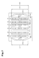
Fig. 7 , element groups G1 to G6, which form the upper and lower arm switching elements, are arranged on amain circuit substrate 200 between a positive input electrode bus bar 201 a and a negative inputelectrode bus bar 202a. Outputelectrode bus bars positive relay electrode 201 b, and anegative relay electrode 202b are arranged between adjacent ones of the element groups G1 to G6, which form the upper and lower arms. The inputelectrode bus bars 201 a and 202a, therelay electrodes electrode bus bars - It is an object of the present invention to provide an inverter device that decreases wire inductance between an input electrode or an output electrode and an element group on a substrate.
- To achieve the above object, one aspect of the present invention is an inverter device for converting power. The inverter device includes a substrate, an upper arm group, a lower arm group, positive and negative input electrodes, and an output electrode. The upper arm group includes a plurality of upper arm elements and serves as an upper arm switching element. The upper arm elements are arranged on the substrate in a single line along a first direction and connected in parallel to each other. The lower arm group includes a plurality of lower arm elements and serves as a lower arm switching element. The lower arm elements are arranged on the substrate in a single line along the first direction and connected in parallel to each other. The positive and negative input electrodes sandwich the upper and lower arm groups on the substrate. Each of the positive and negative electrodes includes a terminal and a bus bar. The output electrode is sandwiched between the upper arm group and the lower arm group on the substrate. The output electrode includes a terminal and a bus bar. At least one of the bus bars of the positive and negative input electrodes and the output electrode extends so that a longitudinal direction of the bus bar is parallel to the first direction. At least one of the bus bars of the positive and negative input electrodes and the output electrode has a length in the longitudinal direction that is greater than a width between two ends of the upper arm elements and the lower arm elements in the first direction.
- Other aspects and advantages of the present invention will become apparent from the following description, taken in conjunction with the accompanying drawings, illustrating by way of example the principles of the invention.
- The invention, together with objects and advantages thereof, may best be understood by reference to the following description of the presently preferred embodiments together with the accompanying drawings in which:
-
Fig. 1 is an exploded perspective view showing an inverter device according to one embodiment of the present invention; -
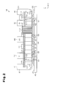
Fig. 2 is a front view showing the inverter device ofFig. 1 ; -
Fig. 3 is a circuit diagram of the inverter device ofFig. 1 ; -
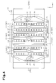
Fig. 4 is a plan view showing a main circuit substrate; -
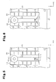
Fig. 5 is a partial schematic plan view showing the main circuit substrate ofFig. 4 ; -
Fig. 6 is a partial schematic plan view showing a main circuit substrate of an inverter device in a comparative example; and -
Fig. 7 is a plan view showing the prior art. - An
inverter device 10 according to one embodiment of the present invention will now be described with reference toFigs. 1 to 6 . Theinverter device 10 is installed in a vehicle. - As viewed in the drawings, X and Y directions extend horizontally, and a Z direction extends vertically.
- Referring to
Figs. 1 and2 , a flat and thin heat sink HS includes a horizontal upper surface. Amain circuit substrate 21 is arranged on the heat sink HS. Acapacitor substrate 100 is arranged to oppose themain circuit substrate 21 above themain circuit substrate 21. Further, a plate-shapedauxiliary bracket 121 is arranged above and opposed to thecapacitor substrate 100. Acontrol circuit substrate 110 is arranged above and opposed to theauxiliary bracket 121. - A plurality of
power elements 20, apositive input electrode 30, anegative input electrode 40, a Uphase output electrode 50, a Vphase output electrode 60, a Wphase output electrode 70, and the like are arranged on themain circuit substrate 21. A plurality ofcapacitors 101 are arranged on thecapacitor substrate 100. Various types ofelectronic components 111 are arranged on thecontrol circuit substrate 110. Further,conductive collars 123 are arranged between theauxiliary bracket 121 and thecontrol circuit substrate 110. - Referring to
Fig. 3 , theinverter device 10 of the present embodiment is a three-phase inverter that supplies a motor with three-phase AC power and converts DC power, which is supplied from a battery, to AC power. As shown inFig. 3 , theinverter device 10 includes a U phase upper arm switching element Q1 and a U phase lower arm switching element Q2. The two switching elements Q1 and Q2 are connected in series with each other. Further, theinverter device 10 includes a V phase upper arm switching element Q3 and a V phase lower arm switching element Q4. The two switching elements Q3 and Q4 are connected in series. Moreover, theinverter device 10 includes a W phase upper arm switching element Q5 and a W phase lower arm switching element Q6. The two switching elements Q5 and Q6 are connected in series. Diodes D1, D2, D3, D4, D5, and D6 are connected in parallel to the switching elements Q1, Q2, Q3, Q4, Q5, and Q6, respectively. The switching elements Q1 to Q6 and the diodes D1 to D6 are mounted on themain circuit substrate 21. - Referring to
Figs. 1 and4 , the upper arm switching element Q1 includes a plurality offirst power elements 20, which form the first element group G1. Thefirst power elements 20 are arranged on themain circuit substrate 21 in a single line along a single direction (Y direction) and connected in parallel to one another. In detail, each of thefirst power elements 20 is a chip including a diode and a switching element that are connected in parallel to each other, and thefirst power element 20 is mounted on themain circuit substrate 21. A MOSFET is used as each of the switching elements. In the same manner, the lower arm switching element Q2 includes a plurality ofsecond power elements 20, which form the second element group G2. Thesecond power elements 20 are arranged on themain circuit substrate 21 in a single line along a single direction (Y direction) and connected in parallel to one another. The lower arm switching element Q3 includes a plurality ofthird power elements 20, which form the third element group G3. Thethird power elements 20 are arranged on themain circuit substrate 21 in a single line along a single direction (Y direction) and connected in parallel to one another. The upper arm switching element Q4 includes a plurality offourth power elements 20, which form the fourth element group G4. Thefourth power elements 20 are arranged on themain circuit substrate 21 in a single line along a single direction (Y direction) and connected in parallel to one another. The upper arm switching element Q5 includes a plurality offifth power elements 20, which form the fifth element group G5. Thefifth power elements 20 are arranged on themain circuit substrate 21 in a single line along a single direction (Y direction) and connected in parallel to one another. The lower arm switching element Q6 includes a plurality ofsixth power elements 20, which form the sixth element group G6. Thesixth power elements 20 are arranged on themain circuit substrate 21 in a single line along a single direction (Y direction) and connected in parallel to one another. - The
first power elements 20, thefourth power elements 20, and thefifth power elements 20 each serve as upper arm elements. The first element group G1, the fourth element group G4, and the fifth element group G5 each serves as an upper arm group. Thesecond power elements 20, thethird power elements 20, and thesixth power elements 20 each serve as lower arm elements. The second element group G2, the third element group G3, and the sixth element group G6 each serves as a lower arm group. - In this manner, the upper switching elements Q1, Q4, and Q5 and the lower switching elements Q2, Q3, and Q6 each include the
power elements 20 that form the corresponding element groups G1 to G6. The first tosixth power elements 20 of each of the switching elements Q1 to Q6 are arranged in lines along the same direction (Y direction) and connected in parallel to one another. A plurality of thepower elements 20 are mounted on the main circuit board inFigs. 1 and4 but are shown in an equivalent manner inFig. 3 to facilitate illustration. - In
Fig. 3 , the Uphase output electrode 50 is connected to a connection node between the U phase upper arm switching element Q1 and the lower arm switching element Q2. The Vphase output electrode 60 is connected to a connection node between the V phase upper arm switching element Q4 and the lower arm switching element Q3. The Wphase output electrode 70 is connected to a connection node between the W phase upper arm switching element Q5 and the lower arm switching element Q6. The Uphase output electrode 50, the Vphase output electrode 60, and the Wphase output electrode 70 are connected to a vehicle travel motor (not shown), which serves as an output device. - In the
main circuit substrate 21 shown inFig. 4 , the drain of the switching element Q1 (first element group G1) is electrically connected to thepositive input electrode 30 by a conductive pattern (not shown). A plurality of conductive patterns are formed on themain circuit substrate 21. The drains of the switching elements Q4 and Q5 (fourth element group G4 and fifth element group G5) are electrically connected to thepositive relay electrode 24 by conductive patterns (not shown), and thepositive relay electrode 24 is electrically connected to thepositive input electrode 30 by a conductive pattern P1 (refer toFig. 4 ). The sources of the switching elements Q2 and Q3 (second element group G2 and third element group G3) are electrically connected to thenegative relay electrode 23 by conductive patterns (not shown), and thenegative relay electrode 23 is electrically connected to thenegative input electrode 40 by a conductive pattern P2 (refer toFig. 4 ). The source of the switching element Q6 (sixth element group G6) is electrically connected to thenegative input electrode 40 by a conductive pattern (not shown). - Referring to
Fig. 3 , a plurality ofcapacitors 101 are connected in parallel between thepositive input electrode 30 and thenegative input electrode 40. Thecapacitors 101 are mounted on thecapacitor substrate 100. - Referring to
Figs. 1 and4 , the positive andnegative input electrodes main circuit substrate 21 so as to. Further, theoutput electrodes main circuit substrate 21. - In detail, the first element group G1, the second element group G2, the third element group G3, the fourth element group G4, the fifth element group G5, and the sixth element group G6 are arranged in order from right to left in the X direction. The
positive input electrode 30 is arranged at the rightmost side in the X direction, and thenegative input electrode 40 is arranged at the leftmost side in the X direction. The Uphase output electrode 50 is arranged between the first element group G1 and the second element group G2 in the X direction. The Vphase output electrode 60 is arranged between the third element group G3 and the fourth element group G4 in the X direction. The Wphase output electrode 70 is arranged between the fifth element group G5 and the sixth element group G6 in the X direction. - The
relay electrodes main circuit substrate 21. In detail, thenegative relay electrode 23 is arranged between the second element group G2 and the third element group G3 in the X direction, and thenegative relay electrode 23 is electrically connected to thenegative input electrode 40 by the conductive pattern P2, as described above. Thepositive relay electrode 24 is arranged between the fourth element group G4 and the fifth element group G5 in the X direction, and thepositive relay electrode 24 is electrically connected to thepositive input electrode 30 by the conductive pattern P1, as described above. - Referring to
Fig. 3 , thecapacitors 101 connect thepositive input electrode 30 and thenegative input electrode 40 of theinverter device 10 to a positive terminal and a negative terminal of a vehicle battery Bc. The gates of the switching elements Q1 to Q6 are connected to theelectronic components 111 of a control circuit through flat cables CF that connect themain circuit substrate 21 and thecontrol circuit substrate 110. Theelectronic components 111 of the control circuit are mounted on the control circuit substrate 110 (refer toFigs. 1 and2 ). Theinverter device 10 is configured so that the control circuit of thecontrol circuit substrate 110 switch-controls the switching elements Q1 to Q6 to supply the vehicle travel motor with power. - Referring to
Figs. 1 and4 , the positive andnegative input electrodes phase output electrodes terminals terminals main circuit substrate 21. - The bus bars 32, 42, 52, 62, and 72 are formed by elongated plates that are tetragonal and narrow. Further, the bus bars 32, 42, 52, 62, and 72 are electrically connected to the conductive patterns in planar contact with the conductive patterns. The rod-shaped
terminals input electrodes output electrodes - The bus bars 32, 42, 52, 62, and 72 are arranged on the
main circuit substrate 21 so that their longitudinal directions are parallel to the direction in which thepower elements 20 are arranged (Y direction) in the element groups G1 to G6. Thebus bar 32 has a length L1 in the longitudinal direction (Y direction) that is greater than the width W1 between the two ends of each of the element groups G1 to G6 in the direction thepower elements 20 are arranged. In the same manner, thebus bar 42 has a length L2 in the longitudinal direction (Y direction) that is greater than the width W1 between the two ends of each of the element groups G1 to G6 in the direction thepower elements 20 are arranged. Thebus bar 52 has a length L3 in the longitudinal direction (Y direction) that is greater than the width W1 between the two ends of each of the element groups G1 to G6 in the direction thepower elements 20 are arranged. Thebus bar 62 has a length L4 in the longitudinal direction (Y direction) that is greater than the width W1 between the two ends of each of the element groups G1 to G6 in the direction thepower elements 20 are arranged. Thebus bar 72 has a length L5 in the longitudinal direction (Y direction) that is greater than the width W1 between the two ends of each of the element groups G1 to G6 in the direction thepower elements 20 are arranged. - In this manner, the bus bars 32, 42, 52, 62, and 72 of the
electrodes main circuit substrate 21 have lengths (Y direction lengths L1, L2, L3, L4, and L5) that are greater than the width W1 between the two ends of each of the element groups G1 to G6 in the direction thepower elements 20 are arranged. - The
negative relay electrode 23 is arranged on themain circuit substrate 21 so that its longitudinal direction is parallel to the direction in which thepower elements 20 are arranged (Y direction) in the element groups G1 to G6. Further, thepositive relay electrode 24 is arranged on themain circuit substrate 21 so that its longitudinal direction is parallel to the direction in which thepower elements 20 are arranged (Y direction) in the element groups G1 to G6. Thenegative relay electrode 23 has a length L10 in the longitudinal direction (Y direction) that is greater than the width W1 between the two ends of each of the element groups G1 to G6 in the direction thepower elements 20 are arranged (Y direction). - Referring to
Figs. 1 and2 , thecapacitor substrate 100 is arranged on upper surfaces of the bus bars 32 and 42 for the positive andnegative input electrodes positive input electrode 30 and thenegative input electrode 40 to thecapacitor substrate 100. Further, the positive andnegative input electrodes terminals - The rod-shaped
terminals phase output electrode 50, the Vphase output electrode 60, and the Wphase output electrode 70 extend through thecapacitor substrate 100. Theauxiliary bracket 121 includes twolegs 122 fixed to themain circuit substrate 21 so that theauxiliary bracket 121 is located above themain circuit substrate 21. The control circuit substrate supports 33 and 43 of the positive andnegative input electrodes auxiliary bracket 121. Further, theterminals phase output electrode 50, the Vphase output electrode 60, and the Wphase output electrode 70 extend through theauxiliary bracket 121. Thecontrol circuit substrate 110 is supported on theauxiliary bracket 121. Further, theterminals phase output electrode 50, the Vphase output electrode 60, and the Wphase output electrode 70 extend through thecontrol circuit substrate 110. Theconductive collars 123 electrically connect the control circuit substrate supports 33 and 43 to thecontrol circuit substrate 110. Acontrol circuit connector 112 is arranged on thecontrol circuit substrate 110 and connected to a flat cable CF. The flat cable CF serves as a connection member and electrically connects themain circuit substrate 21 and thecontrol circuit substrate 110. - The operation of the inverter device will now be described.
- Direct current from the vehicle battery Bc flows to the
main circuit substrate 21 via theinput electrodes relay electrodes power elements 20 of first, fourth, and fifth element groups G1, G4, and G5) and the lower arm switching elements Q2, Q3, and Q6 (power elements 20 of second, third, and sixth element groups G3, G3, and G6) undergo on-off control. Alternating current flows via the Uphase output electrode 50, the Vphase output electrode 60, and the Wphase output electrode 70 to the vehicle travel motor. - When the
positive input electrode 30 and thenegative input electrode 40 are heated, heat is transmitted from the bus bars 32 and 42 via themain circuit substrate 21 to the heat sink HS, which radiates the heat. Further, the heat generated by the switching operation of the switching elements Q1 to Q6 (element groups G1 to G6) is transmitted via themain circuit substrate 21 to the heat sink HS, which radiates the heat. - The flow of current in the
main circuit substrate 21 when the switching elements Q1 to Q6 (element groups G1 to G6) are activated and deactivated will now be described. - Direct current from the vehicle battery Bc is supplied to the
inverter device 10. Then, the control circuit (electronic components 111) activates and deactivates the switching elements Q1 to Q6 (element groups G1 to G6) and output alternating current from theoutput electrodes - As shown in
Fig. 4 , the lengths L1, L2, L3, L4, and L5 of the bus bars 32, 42, 52, 62, and 72 in the longitudinal direction are greater than the width W1 between the two ends of each of the element groups G1 to G6 in the direction thepower elements 20 are arranged. As a result, bus bars allowing for efficient flow of current and including a larger current path than copper patterns formed on a substrate are arranged closer to the ones of the power elements connected in parallel that are arranged at the side farther from the output electrode. This allows for reduction in inductance entirely in the element group for each phase. More specifically, inFig. 7 , with regard to the relationship of dimension L50 of the positive electrode, dimension L51 of the negative electrode, and dimension W50 of the element groups G1 to G6, the dimensions L50 and L51 of the electrodes are smaller than the dimension W50 of the element groups. In this case, wire inductance is apt to increasing. The same applies to the bus bars 203, 204, and 205 for each of the phases. In contrast, in the present embodiment shown inFig. 4 , the lengths L1, L2, L3, L4, and L5 of the bus bars 32, 42, 52, 62, and 72 is greater than the width W1 between the two ends of each of the element groups G1 to G6 in the direction thepower elements 20 are arranged. This reduces the wire inductance. - This will be described in further detail with reference to
Fig. 5 . -
Fig. 5 illustrates the present embodiment and corresponds toFig. 4 . - A case in which the dimensions L50 and L51 of the electrodes is smaller than the dimension W50 of the element groups as shown in
Fig. 7 will now be described. Current i20 flows to the output electrode from thepower elements 20 arranged in a single line and in a single direction on themain circuit substrate 21. Here, as for thepower elements 20 located at the ends, referring toFig. 6 , current flows through a diagonal path toward the bus bar that is electrically connected to the output electrode. The same applies to the other phases ofFig. 7 . - Further, the case of
Fig. 4 in which the lengths L1, L2, L3, L4, and L5 of the bus bars 32, 42, 52, 62, and 72 are greater than the width W 1 between the two ends of each of the element groups G1 to G6 in the direction thepower elements 20 are arranged will now be described. Current i10 flows to the output electrode from thepower elements 20 arranged in a single line and in a single direction on themain circuit substrate 21. Here, as for thepower elements 20 located at the ends, referring toFig. 5 , current flows straight aside through the shortest path toward the bus bar electrically connected to the output electrode. - Thus, in contrast with when the dimension W50 of the element groups G1 to G6 is smaller than the dimensions L50 and L51 of the electrodes (bus bars 201 and 202) as shown
Fig. 7 , when the lengths L1, L2, L3, L4, and L5 of the bus bars 32, 42, 52, 62, and 72 is greater than the width W1 between the two ends of each of the element groups G1 to G6 in the direction thepower elements 20 are arranged, the wire inductance may be reduced. By further shortening the current path when upper arm current is commutated to lower arm current, inductance may be reduced. Further, the current flowing through each of thepower elements 20 in the element groups G1 to G6 may be balanced. As a result, when switching thepower elements 20 at the same switching speed as the prior art, a switching surge voltage may be decreased. Consequently, inexpensive power elements designed for lower voltages may be employed. - Even when increasing the switching speed, the switching surge voltage would be about the same as the prior art. Thus, switching loss may be reduced. Consequently, a compact and inexpensive cooling system (heat sink HS) may be used.
- The same applies to the
relay electrode relay electrodes power elements 20 are arranged. Thus, as described with reference toFigs. 5 and 6 , wire inductance is reduced between therelay electrodes - The present embodiment has the advantages described below.
- (1) The bus bars 32, 42, 52, 62, and 72 are arranged on the
main circuit substrate 21 so that their longitudinal directions is parallel to the direction in which thepower elements 20 are arranged in each of the element groups G1 to G6. The lengths L1, L2, L3, L4, and L5 of the bus bars 32, 42, 52, 62, and 72 in the longitudinal direction is greater than the width W1 between the two ends of each of the element groups G1 to G6 in the direction thepower elements 20 are arranged. Thus, the wire inductance may be reduced on themain circuit substrate 21 between the element groups G1 to G6 and theinput electrodes output electrodes - (2) The element groups G2, G3, G4, and G5 sandwich the
relay electrodes input electrodes main circuit substrate 21. Therelay electrodes main circuit substrate 21 so that their longitudinal directions are parallel to the direction in which thepower elements 20 of the element groups G1 to G6 are arranged. The lengths L10 and L11 in the longitudinal direction of therelay electrodes power elements 20 are arranged. Thus, the wire inductance may be reduced between therelay electrodes main circuit substrate 21. - It should be apparent to those skilled in the art that the present invention may be embodied in many other specific forms without departing from the spirit or scope of the invention. Therefore, the present examples and embodiments are to be considered as illustrative and not restrictive, and the invention is not to be limited to the details given herein, but may be modified within the scope and equivalence of the appended claims.
- An inverter device includes a substrate (21), upper arm elements (20), lower arm elements (20), positive and negative input electrodes (30, 40), and an output electrode (50, 60, 70). The upper arm elements (20) serve as an upper switching element (Q1, Q4, Q5) and are arranged along a first direction (Y). The lower arm elements (20) serve as a lower arm switching element (20) and are arranged along the first direction (Y). At least one of bus bars (32, 42, 52, 62, 72) of the positive and negative input electrodes (30, 40) and the output electrode (50, 60, 70) extends parallel to the first direction (Y). At least one of the bus bars (32, 42, 52, 62, 72) of the positive and negative input electrodes (30, 40) and the output electrode (50, 60, 70) has a length (L1 -L5) in the longitudinal direction that is greater than a width (W1) between two ends of the upper arm elements (20) and the lower arm elements (20) in the first direction (Y).
Claims (4)
- An inverter device for converting power, the inverter device comprising:a substrate (21);an upper arm group (G1, G4, G5) including a plurality of upper arm elements (20) and serving as an upper arm switching element (Q1, Q4, Q5), wherein the upper arm elements (20) are arranged on the substrate (21) in a single line along a first direction (Y) and connected in parallel to each other,a lower arm group (G2, G3, G6) including a plurality of lower arm elements (20) and serving as a lower arm switching element (Q2, Q3, Q6), wherein the lower arm elements (20) are arranged on the substrate (21) in a single line along the first direction (Y) and connected in parallel to each other;positive and negative input electrodes (30, 40) sandwiching the upper and lower arm groups (G1-G6) on the substrate (21), wherein each of the positive and negative electrodes (30, 40) includes a terminal (31, 41) and a bus bar (32, 42); andan output electrode (50, 60, 70) sandwiched between the upper arm group (G1, G4, G5) and the lower arm group (G2, G3, G6) on the substrate (21), wherein the output electrode (50, 60, 70) includes a terminal (51, 61, 71) and a bus bar (52, 62, 72), whereinat least one of the bus bars (32, 42, 52, 62, 72) of the positive and negative input electrodes (30, 40) and the output electrode (50, 60, 70) extends so that a longitudinal direction of the bus bar is parallel to the first direction (Y), andat least one of the bus bars (32, 42, 52, 62, 72) of the positive and negative input electrodes (30, 40) and the output electrode (50, 60, 70) has a length (L1-L5) in the longitudinal direction that is greater than a width (W1) between two ends of the upper arm elements (20) and the lower arm elements (20) in the first direction (Y).
- The inverter device according to claim 1, further comprising a relay electrode (23, 24) connected to the input electrode (30, 40) by a conductive pattern (P1, P2) formed on the substrate (21), wherein
the relay electrode (23, 24) is sandwiched between the upper arm group (G1, G4, G5) and the lower arm group (G2, G3, G6) on the substrate (21),
the relay electrode (23, 24) extends so that a longitudinal direction of the relay electrode (23, 24) is parallel to the first direction (Y), and
the relay electrode (23, 24) has a length (L10, L11) in the longitudinal direction that is greater than the width (W1) between the two ends of the upper arm elements (20) and the lower arm elements (20) in the first direction (Y). - The inverter device according to claim 1, wherein the inverter device is a three-phase inverter that supplies three-phase AC power to a motor.
- The inverter device according to claim 1, wherein
each of the bus bars (32, 42, 52, 62, 72) of the positive and negative input electrodes (30, 40) and the output electrodes (50, 60, 70) extends so that a longitudinal direction of the bus bar (32, 42, 52, 62, 72) is parallel to the first direction (Y), and
each of the bus bars (32, 42, 52, 62, 72) of the positive and negative input electrodes (30, 40) and the output electrodes (50, 60, 70) has a length (L1-L5) in the longitudinal direction that is greater than the width (W1) between the two ends of the upper arm elements (20) and the lower arm elements (20) in the first direction (Y).
Applications Claiming Priority (1)
| Application Number | Priority Date | Filing Date | Title |
|---|---|---|---|
| JP2012156717A JP5708583B2 (en) | 2012-07-12 | 2012-07-12 | Inverter device |
Publications (2)
| Publication Number | Publication Date |
|---|---|
| EP2685796A2 true EP2685796A2 (en) | 2014-01-15 |
| EP2685796A3 EP2685796A3 (en) | 2017-03-22 |
Family
ID=48747465
Family Applications (1)
| Application Number | Title | Priority Date | Filing Date |
|---|---|---|---|
| EP13175868.2A Withdrawn EP2685796A3 (en) | 2012-07-12 | 2013-07-10 | Inverter device |
Country Status (4)
| Country | Link |
|---|---|
| US (1) | US9385629B2 (en) |
| EP (1) | EP2685796A3 (en) |
| JP (1) | JP5708583B2 (en) |
| CN (1) | CN103546015B (en) |
Cited By (3)
| Publication number | Priority date | Publication date | Assignee | Title |
|---|---|---|---|---|
| EP3609068A1 (en) * | 2018-08-07 | 2020-02-12 | Mahle International GmbH | Electric power inverter |
| WO2021044062A1 (en) * | 2019-09-06 | 2021-03-11 | Valeo Systemes De Controle Moteur | Electronic board for voltage converter |
| EP3944477A1 (en) * | 2020-07-22 | 2022-01-26 | Mahle International GmbH | Inverter and electric motor having such an inverter |
Families Citing this family (14)
| Publication number | Priority date | Publication date | Assignee | Title |
|---|---|---|---|---|
| JP6665926B2 (en) * | 2016-03-22 | 2020-03-13 | 富士電機株式会社 | Semiconductor device and method of manufacturing semiconductor device |
| JP6685424B2 (en) * | 2016-11-11 | 2020-04-22 | 三菱電機株式会社 | Power converter and air conditioner using the same |
| JP6801578B2 (en) * | 2017-05-17 | 2020-12-16 | 株式会社豊田自動織機 | Electronics |
| JP2019068648A (en) * | 2017-10-02 | 2019-04-25 | 株式会社豊田自動織機 | Inverter device |
| JP6863307B2 (en) * | 2018-02-02 | 2021-04-21 | 株式会社豊田自動織機 | Inverter |
| US11223305B2 (en) * | 2018-11-16 | 2022-01-11 | Toyota Jidosha Kabushiki Kaisha | Vehicle driving device |
| JP7088124B2 (en) * | 2019-04-25 | 2022-06-21 | 株式会社豊田自動織機 | Semiconductor device |
| JP2021158867A (en) * | 2020-03-30 | 2021-10-07 | 株式会社ミツバ | Driving device |
| JP7505450B2 (en) * | 2021-06-14 | 2024-06-25 | 株式会社豊田自動織機 | Power Conversion Equipment |
| JP7317182B1 (en) * | 2022-05-23 | 2023-07-28 | 三菱電機株式会社 | Semiconductor device and its manufacturing method |
| WO2025057415A1 (en) * | 2023-09-15 | 2025-03-20 | 株式会社デンソーテン | Electronic apparatus and inverter device |
| WO2025057421A1 (en) * | 2023-09-15 | 2025-03-20 | 株式会社デンソーテン | Electronic device and electronic device manufacturing method |
| WO2025069542A1 (en) * | 2023-09-29 | 2025-04-03 | 株式会社ミツバ | Motor control device |
| WO2025069541A1 (en) * | 2023-09-29 | 2025-04-03 | 株式会社ミツバ | Motor control device |
Citations (3)
| Publication number | Priority date | Publication date | Assignee | Title |
|---|---|---|---|---|
| JPH03173511A (en) | 1989-12-01 | 1991-07-26 | Kazumasa Takahashi | Aging device for flavored food |
| US20030030481A1 (en) * | 2001-08-08 | 2003-02-13 | Mitsubishi Denki Kabushiki Kaisha | Power module |
| EP2023473B1 (en) * | 2007-08-09 | 2019-02-13 | Hitachi, Ltd. | Power inverter |
Family Cites Families (7)
| Publication number | Priority date | Publication date | Assignee | Title |
|---|---|---|---|---|
| JPH073851B2 (en) * | 1988-01-28 | 1995-01-18 | 富士電機株式会社 | Parallel connection of power transistors |
| JP3809346B2 (en) * | 2001-06-15 | 2006-08-16 | トヨタ自動車株式会社 | Switching circuit |
| JP5120604B2 (en) * | 2007-05-22 | 2013-01-16 | アイシン・エィ・ダブリュ株式会社 | Semiconductor module and inverter device |
| JP4708459B2 (en) * | 2008-07-29 | 2011-06-22 | 日立オートモティブシステムズ株式会社 | Power converter |
| CN201532949U (en) * | 2009-09-27 | 2010-07-21 | 北京东标电子有限公司 | An Insulated Gate Bipolar Transistor System |
| JP3173512U (en) * | 2011-11-25 | 2012-02-09 | 株式会社豊田自動織機 | Semiconductor device |
| JP3173511U (en) | 2011-11-25 | 2012-02-09 | 株式会社豊田自動織機 | Semiconductor device |
-
2012
- 2012-07-12 JP JP2012156717A patent/JP5708583B2/en not_active Expired - Fee Related
-
2013
- 2013-07-08 CN CN201310284509.9A patent/CN103546015B/en not_active Expired - Fee Related
- 2013-07-10 US US13/938,852 patent/US9385629B2/en not_active Expired - Fee Related
- 2013-07-10 EP EP13175868.2A patent/EP2685796A3/en not_active Withdrawn
Patent Citations (3)
| Publication number | Priority date | Publication date | Assignee | Title |
|---|---|---|---|---|
| JPH03173511A (en) | 1989-12-01 | 1991-07-26 | Kazumasa Takahashi | Aging device for flavored food |
| US20030030481A1 (en) * | 2001-08-08 | 2003-02-13 | Mitsubishi Denki Kabushiki Kaisha | Power module |
| EP2023473B1 (en) * | 2007-08-09 | 2019-02-13 | Hitachi, Ltd. | Power inverter |
Cited By (6)
| Publication number | Priority date | Publication date | Assignee | Title |
|---|---|---|---|---|
| EP3609068A1 (en) * | 2018-08-07 | 2020-02-12 | Mahle International GmbH | Electric power inverter |
| WO2021044062A1 (en) * | 2019-09-06 | 2021-03-11 | Valeo Systemes De Controle Moteur | Electronic board for voltage converter |
| FR3100668A1 (en) * | 2019-09-06 | 2021-03-12 | Valeo Systemes De Controle Moteur | Electronic board for voltage converter |
| US20220322559A1 (en) * | 2019-09-06 | 2022-10-06 | Valeo Systemes De Controle Moteur | Electronic board for voltage converter |
| US11950388B2 (en) * | 2019-09-06 | 2024-04-02 | Valeo Systemes De Controle Moteur | Electronic board for voltage converter |
| EP3944477A1 (en) * | 2020-07-22 | 2022-01-26 | Mahle International GmbH | Inverter and electric motor having such an inverter |
Also Published As
| Publication number | Publication date |
|---|---|
| JP2014023181A (en) | 2014-02-03 |
| EP2685796A3 (en) | 2017-03-22 |
| CN103546015B (en) | 2016-03-16 |
| CN103546015A (en) | 2014-01-29 |
| US20140015452A1 (en) | 2014-01-16 |
| JP5708583B2 (en) | 2015-04-30 |
| US9385629B2 (en) | 2016-07-05 |
Similar Documents
| Publication | Publication Date | Title |
|---|---|---|
| EP2685796A2 (en) | Inverter device | |
| US9006883B2 (en) | Semiconductor module with switching elements | |
| KR101546993B1 (en) | Power conversion apparatus | |
| CN112217382B (en) | Flying capacitor circuit, circuit module and power conversion device | |
| US9906154B2 (en) | Power conversion unit and power conversion device | |
| JP2021078233A (en) | Electric power conversion system | |
| CN108476561B (en) | Induction heating power supply apparatus | |
| US20160141973A1 (en) | Printed circuit board power cell | |
| CN103856068B (en) | Power-converting device | |
| TW201503585A (en) | Inverter with parallel power devices | |
| CN104380587B (en) | Power conversion device | |
| JP6794841B2 (en) | Power converter and its manufacturing method | |
| JP2014049475A (en) | Inverter device | |
| CN111953263B (en) | Motor drive equipment and motor operation systems | |
| JP6170640B1 (en) | Gate drive board with parallel connector | |
| CN105790704A (en) | Junction box for solar cell | |
| JP2018007501A (en) | Semiconductor device | |
| US20190260301A1 (en) | Switching power supply device | |
| JP2019102477A (en) | Circuit module | |
| KR101611885B1 (en) | Inverter Stack | |
| TWI624138B (en) | Stacked inverter | |
| JP2019037098A (en) | Three-level inverter unit and three-phase inverter device using the same |
Legal Events
| Date | Code | Title | Description |
|---|---|---|---|
| PUAI | Public reference made under article 153(3) epc to a published international application that has entered the european phase |
Free format text: ORIGINAL CODE: 0009012 |
|
| 17P | Request for examination filed |
Effective date: 20130710 |
|
| AK | Designated contracting states |
Kind code of ref document: A2 Designated state(s): AL AT BE BG CH CY CZ DE DK EE ES FI FR GB GR HR HU IE IS IT LI LT LU LV MC MK MT NL NO PL PT RO RS SE SI SK SM TR |
|
| AX | Request for extension of the european patent |
Extension state: BA ME |
|
| PUAL | Search report despatched |
Free format text: ORIGINAL CODE: 0009013 |
|
| AK | Designated contracting states |
Kind code of ref document: A3 Designated state(s): AL AT BE BG CH CY CZ DE DK EE ES FI FR GB GR HR HU IE IS IT LI LT LU LV MC MK MT NL NO PL PT RO RS SE SI SK SM TR |
|
| AX | Request for extension of the european patent |
Extension state: BA ME |
|
| RIC1 | Information provided on ipc code assigned before grant |
Ipc: H02M 7/537 20060101ALI20170213BHEP Ipc: H05K 7/14 20060101AFI20170213BHEP |
|
| STAA | Information on the status of an ep patent application or granted ep patent |
Free format text: STATUS: EXAMINATION IS IN PROGRESS |
|
| 17Q | First examination report despatched |
Effective date: 20200420 |
|
| STAA | Information on the status of an ep patent application or granted ep patent |
Free format text: STATUS: THE APPLICATION IS DEEMED TO BE WITHDRAWN |
|
| 18D | Application deemed to be withdrawn |
Effective date: 20240201 |