EP2748878B1 - Dispositif électroluminescent organique - Google Patents
Dispositif électroluminescent organique Download PDFInfo
- Publication number
- EP2748878B1 EP2748878B1 EP12740070.3A EP12740070A EP2748878B1 EP 2748878 B1 EP2748878 B1 EP 2748878B1 EP 12740070 A EP12740070 A EP 12740070A EP 2748878 B1 EP2748878 B1 EP 2748878B1
- Authority
- EP
- European Patent Office
- Prior art keywords
- etm2
- etm1
- aromatic
- atoms
- organic electroluminescent
- Prior art date
- Legal status (The legal status is an assumption and is not a legal conclusion. Google has not performed a legal analysis and makes no representation as to the accuracy of the status listed.)
- Active
Links
- 0 Cc1cc(*c2cc(-c(c(*3)cc(C)c4)c4I)c3cc2-2)c-2c(*)c1 Chemical compound Cc1cc(*c2cc(-c(c(*3)cc(C)c4)c4I)c3cc2-2)c-2c(*)c1 0.000 description 6
- UCZUGRJDEXQWJF-UHFFFAOYSA-N C(c1cc(-c2ccccc2)ccc1)[n+]1c(-c2cc(-c3ccccc3)ccc2)nc(-c(cc2C34c5ccccc5-c5ccccc35)ccc2-c(cc2)c4cc2-c2nc(-c3cc(-c4ccccc4)ccc3)nc(-c3cccc(-c4ccccc4)c3)n2)[n-]1 Chemical compound C(c1cc(-c2ccccc2)ccc1)[n+]1c(-c2cc(-c3ccccc3)ccc2)nc(-c(cc2C34c5ccccc5-c5ccccc35)ccc2-c(cc2)c4cc2-c2nc(-c3cc(-c4ccccc4)ccc3)nc(-c3cccc(-c4ccccc4)c3)n2)[n-]1 UCZUGRJDEXQWJF-UHFFFAOYSA-N 0.000 description 1
- XUSYMACRPHWJFJ-ONNFQVAWSA-N C/C=C(\C=C)/c1ccccc1 Chemical compound C/C=C(\C=C)/c1ccccc1 XUSYMACRPHWJFJ-ONNFQVAWSA-N 0.000 description 1
- DQXRDVAWDYYSLQ-UHFFFAOYSA-N CC(C)(C)c(cc1C(C2C=CC=CC22)(c3c2cccc3)c2c3)ccc1-c2ccc3-c1nc(-c2ccccc2)nc(-c2ccccc2)n1 Chemical compound CC(C)(C)c(cc1C(C2C=CC=CC22)(c3c2cccc3)c2c3)ccc1-c2ccc3-c1nc(-c2ccccc2)nc(-c2ccccc2)n1 DQXRDVAWDYYSLQ-UHFFFAOYSA-N 0.000 description 1
- HTEVCXRXRAWQHM-UHFFFAOYSA-N CC(C)(C1C=CC=CC1c1c2)c1cc1c2c2ccccc2[n]1-c1cccc(-c2nc(-c3ccccc3)nc(-c3ccccc3)c2)c1 Chemical compound CC(C)(C1C=CC=CC1c1c2)c1cc1c2c2ccccc2[n]1-c1cccc(-c2nc(-c3ccccc3)nc(-c3ccccc3)c2)c1 HTEVCXRXRAWQHM-UHFFFAOYSA-N 0.000 description 1
- YQIQKTOKMDHBSP-UHFFFAOYSA-N CC(C)(c(cccc1)c1-c1c2)c1cc1c2c(cccc2)c2[n]1-c1nc(-c2ccccc2)nc(-c2ccccc2)n1 Chemical compound CC(C)(c(cccc1)c1-c1c2)c1cc1c2c(cccc2)c2[n]1-c1nc(-c2ccccc2)nc(-c2ccccc2)n1 YQIQKTOKMDHBSP-UHFFFAOYSA-N 0.000 description 1
- WHKXLDLTMHXNDC-UHFFFAOYSA-N CC(C)(c1ccccc1-c1c2)c1cc1c2c2ccccc2[n]1-c1nc(-c2cc(-c3ccccc3)ccc2)cc(-c2cccc(-c3ccccc3)c2)n1 Chemical compound CC(C)(c1ccccc1-c1c2)c1cc1c2c2ccccc2[n]1-c1nc(-c2cc(-c3ccccc3)ccc2)cc(-c2cccc(-c3ccccc3)c2)n1 WHKXLDLTMHXNDC-UHFFFAOYSA-N 0.000 description 1
- MWDIBJDLZCVWKI-UHFFFAOYSA-N CC1(C)c(cc(c(c2c3cccc2)c2)[n]3-c(cc3)ccc3-c(cc3)ccc3-[n](c(cccc3)c3c3c4)c3cc3c4-c4ccccc4C3(C)C)c2-c2c1cccc2 Chemical compound CC1(C)c(cc(c(c2c3cccc2)c2)[n]3-c(cc3)ccc3-c(cc3)ccc3-[n](c(cccc3)c3c3c4)c3cc3c4-c4ccccc4C3(C)C)c2-c2c1cccc2 MWDIBJDLZCVWKI-UHFFFAOYSA-N 0.000 description 1
- XEVUOHQIROTSEI-UHFFFAOYSA-N O=C(c1cc(-c2cccc(Oc3ccccc3)c2)cc(-c2cccc(Oc3ccccc3)c2)c1)c1cc(-c2cccc(Oc3ccccc3)c2)cc(-c2cc(Oc3ccccc3)ccc2)c1 Chemical compound O=C(c1cc(-c2cccc(Oc3ccccc3)c2)cc(-c2cccc(Oc3ccccc3)c2)c1)c1cc(-c2cccc(Oc3ccccc3)c2)cc(-c2cc(Oc3ccccc3)ccc2)c1 XEVUOHQIROTSEI-UHFFFAOYSA-N 0.000 description 1
- STDGLPVNLFWZEP-UHFFFAOYSA-N O=C(c1cc(N(c2ccccc2)c2ccccc2)cc(N(c2ccccc2)c2ccccc2)c1)c1cc(N(c2ccccc2)c2ccccc2)cc(N(c2ccccc2)c2ccccc2)c1 Chemical compound O=C(c1cc(N(c2ccccc2)c2ccccc2)cc(N(c2ccccc2)c2ccccc2)c1)c1cc(N(c2ccccc2)c2ccccc2)cc(N(c2ccccc2)c2ccccc2)c1 STDGLPVNLFWZEP-UHFFFAOYSA-N 0.000 description 1
- VBNYIIXPGGDMGR-UHFFFAOYSA-N OP(c1ccccc1)(c1ccccc1)c1cc(P(c2ccccc2)(c2ccccc2)=O)cc(C(c2cc(P(c3ccccc3)(c3ccccc3)=O)cc(P(c3ccccc3)(c3ccccc3)=O)c2)=O)c1 Chemical compound OP(c1ccccc1)(c1ccccc1)c1cc(P(c2ccccc2)(c2ccccc2)=O)cc(C(c2cc(P(c3ccccc3)(c3ccccc3)=O)cc(P(c3ccccc3)(c3ccccc3)=O)c2)=O)c1 VBNYIIXPGGDMGR-UHFFFAOYSA-N 0.000 description 1
- YRPWMUKELOXRLZ-UHFFFAOYSA-N c(cc1)cc2c1-c1ccccc1C21c(cc(cc2)-c3nc(-c(cc4)ccc4-[n]4c(cccc5)c5c5c4cccc5)nc(-c(cc4)ccc4-[n]4c5ccccc5c5c4cccc5)n3)c2-c2c1cccc2 Chemical compound c(cc1)cc2c1-c1ccccc1C21c(cc(cc2)-c3nc(-c(cc4)ccc4-[n]4c(cccc5)c5c5c4cccc5)nc(-c(cc4)ccc4-[n]4c5ccccc5c5c4cccc5)n3)c2-c2c1cccc2 YRPWMUKELOXRLZ-UHFFFAOYSA-N 0.000 description 1
- TYFHSSLJWYHFOI-UHFFFAOYSA-N c(cc1)cc2c1-c1ccccc1C21c2cc(-c3nc(-c4cccc5ccccc45)nc(-c4cccc5c4cccc5)n3)ccc2-c2ccccc12 Chemical compound c(cc1)cc2c1-c1ccccc1C21c2cc(-c3nc(-c4cccc5ccccc45)nc(-c4cccc5c4cccc5)n3)ccc2-c2ccccc12 TYFHSSLJWYHFOI-UHFFFAOYSA-N 0.000 description 1
- CHMJVLZKNBPRHB-UHFFFAOYSA-N c(cc1)ccc1-c(cc1)ccc1-c1nc(-c2ccc3-c4ccccc4C4(c5ccccc5-c5ccccc45)c3c2)nc(-c(cc2)cc3c2-c2ccccc2C32c3ccccc3-c3c2cccc3)n1 Chemical compound c(cc1)ccc1-c(cc1)ccc1-c1nc(-c2ccc3-c4ccccc4C4(c5ccccc5-c5ccccc45)c3c2)nc(-c(cc2)cc3c2-c2ccccc2C32c3ccccc3-c3c2cccc3)n1 CHMJVLZKNBPRHB-UHFFFAOYSA-N 0.000 description 1
- HKGFWIMVEQEHKE-UHFFFAOYSA-N c(cc1)ccc1-c1nc(-c(cc2)cc(C34c5ccccc5-c5c3cccc5)c2-c(cc2)c4cc2-c2nc(-c3ccccc3)nc(-c3ccccc3)n2)nc(-c2ccccc2)n1 Chemical compound c(cc1)ccc1-c1nc(-c(cc2)cc(C34c5ccccc5-c5c3cccc5)c2-c(cc2)c4cc2-c2nc(-c3ccccc3)nc(-c3ccccc3)n2)nc(-c2ccccc2)n1 HKGFWIMVEQEHKE-UHFFFAOYSA-N 0.000 description 1
- HQSUATXMIIPUDI-UHFFFAOYSA-N c(cc1)ccc1-c1nc(-c2ccccc2)nc(-c(cc2)cc(C34c(cccc5)c5-c5c3cccc5)c2-c2c4ccc(-[n]3c(cccc4)c4c4c3cccc4)c2)n1 Chemical compound c(cc1)ccc1-c1nc(-c2ccccc2)nc(-c(cc2)cc(C34c(cccc5)c5-c5c3cccc5)c2-c2c4ccc(-[n]3c(cccc4)c4c4c3cccc4)c2)n1 HQSUATXMIIPUDI-UHFFFAOYSA-N 0.000 description 1
- VPNHDXICUCAAOD-UHFFFAOYSA-N c1ccc(C2(c(cc(cc3)-c4nc(-c5cccc6ccccc56)nc(-c5cccc6c5cccc6)n4)c3-c3c2cccc3)c2ccccc2)cc1 Chemical compound c1ccc(C2(c(cc(cc3)-c4nc(-c5cccc6ccccc56)nc(-c5cccc6c5cccc6)n4)c3-c3c2cccc3)c2ccccc2)cc1 VPNHDXICUCAAOD-UHFFFAOYSA-N 0.000 description 1
Classifications
-
- C—CHEMISTRY; METALLURGY
- C09—DYES; PAINTS; POLISHES; NATURAL RESINS; ADHESIVES; COMPOSITIONS NOT OTHERWISE PROVIDED FOR; APPLICATIONS OF MATERIALS NOT OTHERWISE PROVIDED FOR
- C09B—ORGANIC DYES OR CLOSELY-RELATED COMPOUNDS FOR PRODUCING DYES, e.g. PIGMENTS; MORDANTS; LAKES
- C09B57/00—Other synthetic dyes of known constitution
-
- H—ELECTRICITY
- H10—SEMICONDUCTOR DEVICES; ELECTRIC SOLID-STATE DEVICES NOT OTHERWISE PROVIDED FOR
- H10K—ORGANIC ELECTRIC SOLID-STATE DEVICES
- H10K50/00—Organic light-emitting devices
- H10K50/10—OLEDs or polymer light-emitting diodes [PLED]
- H10K50/11—OLEDs or polymer light-emitting diodes [PLED] characterised by the electroluminescent [EL] layers
-
- H—ELECTRICITY
- H10—SEMICONDUCTOR DEVICES; ELECTRIC SOLID-STATE DEVICES NOT OTHERWISE PROVIDED FOR
- H10K—ORGANIC ELECTRIC SOLID-STATE DEVICES
- H10K50/00—Organic light-emitting devices
- H10K50/10—OLEDs or polymer light-emitting diodes [PLED]
- H10K50/14—Carrier transporting layers
- H10K50/16—Electron transporting layers
- H10K50/165—Electron transporting layers comprising dopants
-
- H—ELECTRICITY
- H10—SEMICONDUCTOR DEVICES; ELECTRIC SOLID-STATE DEVICES NOT OTHERWISE PROVIDED FOR
- H10K—ORGANIC ELECTRIC SOLID-STATE DEVICES
- H10K71/00—Manufacture or treatment specially adapted for the organic devices covered by this subclass
-
- H—ELECTRICITY
- H10—SEMICONDUCTOR DEVICES; ELECTRIC SOLID-STATE DEVICES NOT OTHERWISE PROVIDED FOR
- H10K—ORGANIC ELECTRIC SOLID-STATE DEVICES
- H10K85/00—Organic materials used in the body or electrodes of devices covered by this subclass
- H10K85/60—Organic compounds having low molecular weight
- H10K85/649—Aromatic compounds comprising a hetero atom
- H10K85/654—Aromatic compounds comprising a hetero atom comprising only nitrogen as heteroatom
-
- H—ELECTRICITY
- H10—SEMICONDUCTOR DEVICES; ELECTRIC SOLID-STATE DEVICES NOT OTHERWISE PROVIDED FOR
- H10K—ORGANIC ELECTRIC SOLID-STATE DEVICES
- H10K2101/00—Properties of the organic materials covered by group H10K85/00
- H10K2101/10—Triplet emission
-
- H—ELECTRICITY
- H10—SEMICONDUCTOR DEVICES; ELECTRIC SOLID-STATE DEVICES NOT OTHERWISE PROVIDED FOR
- H10K—ORGANIC ELECTRIC SOLID-STATE DEVICES
- H10K2101/00—Properties of the organic materials covered by group H10K85/00
- H10K2101/30—Highest occupied molecular orbital [HOMO], lowest unoccupied molecular orbital [LUMO] or Fermi energy values
-
- H—ELECTRICITY
- H10—SEMICONDUCTOR DEVICES; ELECTRIC SOLID-STATE DEVICES NOT OTHERWISE PROVIDED FOR
- H10K—ORGANIC ELECTRIC SOLID-STATE DEVICES
- H10K2101/00—Properties of the organic materials covered by group H10K85/00
- H10K2101/40—Interrelation of parameters between multiple constituent active layers or sublayers, e.g. HOMO values in adjacent layers
-
- H—ELECTRICITY
- H10—SEMICONDUCTOR DEVICES; ELECTRIC SOLID-STATE DEVICES NOT OTHERWISE PROVIDED FOR
- H10K—ORGANIC ELECTRIC SOLID-STATE DEVICES
- H10K71/00—Manufacture or treatment specially adapted for the organic devices covered by this subclass
- H10K71/10—Deposition of organic active material
- H10K71/16—Deposition of organic active material using physical vapour deposition [PVD], e.g. vacuum deposition or sputtering
- H10K71/164—Deposition of organic active material using physical vapour deposition [PVD], e.g. vacuum deposition or sputtering using vacuum deposition
-
- H—ELECTRICITY
- H10—SEMICONDUCTOR DEVICES; ELECTRIC SOLID-STATE DEVICES NOT OTHERWISE PROVIDED FOR
- H10K—ORGANIC ELECTRIC SOLID-STATE DEVICES
- H10K85/00—Organic materials used in the body or electrodes of devices covered by this subclass
- H10K85/40—Organosilicon compounds, e.g. TIPS pentacene
-
- H—ELECTRICITY
- H10—SEMICONDUCTOR DEVICES; ELECTRIC SOLID-STATE DEVICES NOT OTHERWISE PROVIDED FOR
- H10K—ORGANIC ELECTRIC SOLID-STATE DEVICES
- H10K85/00—Organic materials used in the body or electrodes of devices covered by this subclass
- H10K85/60—Organic compounds having low molecular weight
- H10K85/615—Polycyclic condensed aromatic hydrocarbons, e.g. anthracene
- H10K85/626—Polycyclic condensed aromatic hydrocarbons, e.g. anthracene containing more than one polycyclic condensed aromatic rings, e.g. bis-anthracene
-
- H—ELECTRICITY
- H10—SEMICONDUCTOR DEVICES; ELECTRIC SOLID-STATE DEVICES NOT OTHERWISE PROVIDED FOR
- H10K—ORGANIC ELECTRIC SOLID-STATE DEVICES
- H10K85/00—Organic materials used in the body or electrodes of devices covered by this subclass
- H10K85/60—Organic compounds having low molecular weight
- H10K85/649—Aromatic compounds comprising a hetero atom
- H10K85/657—Polycyclic condensed heteroaromatic hydrocarbons
- H10K85/6572—Polycyclic condensed heteroaromatic hydrocarbons comprising only nitrogen in the heteroaromatic polycondensed ring system, e.g. phenanthroline or carbazole
Definitions
- the present invention relates to organic electroluminescent devices which contain a mixture of at least two purely organic materials in the electron transport layer.
- OLEDs organic electroluminescent devices
- organic semiconductors in which organic semiconductors are used as functional materials is, for example, in US 4539507 , US 5151629 , EP 0676461 and WO 98/27136 described.
- Organic electroluminescent devices based on low-molecular compounds are typically composed of a plurality of organic layers which are applied to one another, such as, for example, hole transport layer, emitting layer and electron transport layer.
- the emitting layer can be fluorescent or phosphorescent.
- HOMO highest occupied molecular orbital
- LUMO lowest unoccupied molecular orbital
- the technical problem on which the present invention is based is therefore the provision of electron transport layers for organic electroluminescent devices which do not have the above-mentioned problem.
- An improvement in the charge balance manifests itself in particular in an improved efficiency, an improved service life and usually a reduced operating voltage.
- the aim is to provide electron transport layers that can be used in combination with both fluorescent and phosphorescent emitter layers.
- AlQ 3 aluminum trishydroxyquinolinate
- other metal hydroxyquinolinates are used.
- these are not suitable in combination with triplet emitters, in particular with green and blue emitting triplet emitters, since they do not have a sufficiently high triplet level.
- Hydroxyquinoline also has the disadvantage that it is mutagenic and therefore entails considerable health risks.
- Triazine derivatives are also used as electron transport materials.
- Triazine derivatives have generally proven to be very good electron transport materials, but they also show the problem mentioned above that they are found in some Device structures transport too many electrons into the emitter layer and therefore do not lead to a balanced charge balance.
- LiQ lithium hydroxyquinolinate
- EP 1286568 discloses an electron transport layer for an organic electroluminescent device in which an anthracene derivative is used as a "color-neutral dopant" in the emitting layer and in the electron transport layer adjacent to the emitting layer.
- This "color-neutral dopant" is used in the electron transport layer in combination with AlQ 3 as the electron transport material. It is essential to the invention here that the “color-neutral dopant” comprises an anthracene derivative.
- This device structure is not suitable for phosphorescent emission layers, since phosphorescence is at least partially extinguished by anthracene derivatives.
- the LUMO of the color-neutral dopant is lower than that of AIQ, so that the dopant actively participates in electron transport.
- a fluorescent organic electroluminescent device which has a hole blocking layer and which has a mixture of at least two materials in the electron transport layer, one material being a polycyclic aromatic hydrocarbon, e.g. B. is an anthracene or naphthacene derivative.
- the presence of an additional hole blocking layer is essential to the invention. This is a significant technical disadvantage because the use of an additional layer means an increased technical outlay.
- OLEDs with electron transport layers are already mentioned, which consist of a mixed layer.
- organic electron transport layers for use in organic electroluminescent devices have advantages if they consist of a mixture of at least two purely organic materials, one material being an electron-transporting material and the other material being a material which is not or not significantly important Participates in electron transport in the layer. This is achieved by observing certain relative values for the HOMO and LUMO positions of the materials. Furthermore, both materials have a certain minimum triplet energy. With such electroluminescent devices, improvements, in particular with regard to efficiency, lifetime and operating voltage, are achieved compared to electroluminescent devices which contain only one material in the electron transport layer or which contain mixtures according to the prior art in the electron transport layer. Such electron transport layers are also equally suitable for fluorescent and phosphorescent emitter layers.
- ETM1 and ETM2 in particular HOMO, LUMO, triplet energy and energy gap, are determined as described in detail in the example section in general.
- the organic electroluminescent device according to the invention contains anode, cathode, at least one emitting layer which is arranged between the anode and the cathode, and the electron transport layer according to the invention.
- the organic electroluminescent device does not necessarily have to contain only layers which are made up of organic or organometallic materials. It is also possible for the anode, cathode and / or one or more layers to contain inorganic materials or to be composed entirely of inorganic materials.
- the materials ETM1 and ETM2 are purely organic materials, that is to say that they contain no metals.
- the organic electroluminescent device according to the invention contains further materials in the electron transport layer in addition to ETM1 and ETM2, all further materials preferably have a triplet energy T 1 > 2.2 eV. In addition, in the case of other materials in the electron transport layer, all other materials preferably have a LUMO> LUMO (ETM1).
- the materials ETM1 and ETM2 preferably have a glass transition temperature T G of greater than 80 ° C., particularly preferably greater than 100 ° C., very particularly preferably greater than 120 ° C.
- the triplet energy T 1 of ETM1 and ETM2 and of any further materials present in the electron transport layer is> 2.4 eV, particularly preferably> 2.6 eV, very particularly preferably> 2.7 eV.
- the material ETM1 is preferably an electron-transporting material.
- An electron transporting material in the sense this application is characterized by a LUMO in the range from -3.2 to -2.0 eV.
- ETM1 preferably has a LUMO in the range from -3.1 eV to -2.2 eV, particularly preferably in the range from -3.0 eV to -2.4 eV, very particularly preferably in the range from -2.9 eV to -2.5 eV.
- the material ETM2 is preferably a material that does not or not significantly participate in the electron transport in the electron transport layer. This is ensured by the LUMO of ETM2 being larger than the LUMO of ETM1.
- the LUMO of ETM2 is preferably at least 0.1 eV larger than the LUMO of ETM1, particularly preferably at least 0.2 eV.
- the HOMO of ETM1 is ⁇ -5.3 eV.
- ETM1 HOMO
- ETM2 HOMO
- ETM2 HOMO
- ETM2 HOMO
- ETM1 HOMO
- ETM2 HOMO
- ETM2 HOMO
- ETM2 HOMO
- ETM1 HOMO of the emitting layer or the material of the emitting layer that has the highest HOMO.
- the quantity ratio between ETM1 and ETM2 can vary. In particular, by varying this ratio, the charge balance of the OLED can be set simply and reproducibly. By adjusting the mixing ratio, the efficiency of the OLED can be easily optimized.
- the proportion of ETM2 is preferably ⁇ 10% by volume, particularly preferably ⁇ 30% by volume and very particularly preferably ⁇ 50% by volume.
- the proportion of ETM2 is also preferably 90 90% by volume and particularly preferably 80 80% by volume.
- the electron transport layer contains no further materials apart from the materials ETM1 and ETM2.
- ETM1 and ETM2 which are present in the electron transport layer according to the invention, are described below.
- ETM1 is an electron transporting connection.
- all electron-transporting compounds are suitable for which the above-mentioned condition regarding the T 1 level is fulfilled.
- Preferred electron-transporting compounds are selected from the group consisting of compounds containing six-ring heteroaryl groups, in particular triazine derivatives, pyrimidine derivatives, pyridine derivatives, pyrazine derivatives, quinoxaline derivatives or quinoline derivatives, and compounds containing five-ring heteroaromatics with at least two heteroatoms, in particular oxadiazole derivatives and benzimidazole derivatives.
- Aromatic ketones, lactams, boranes, diazaphosphole derivatives and phosphine oxide derivatives are also suitable.
- Triazine and pyrimidine derivatives are particularly preferably used as ETM1.
- An aryl group in the sense of this invention contains at least 6 carbon atoms;
- a heteroaryl group in the sense of this invention contains at least 2 carbon atoms and at least 1 heteroatom, with the proviso that the sum of carbon atoms and heteroatoms is at least 5.
- the heteroatoms are preferably selected from N, O and / or S.
- an aryl group or heteroaryl group is either a simple aromatic cycle, i.e.
- benzene or a simple heteroaromatic cycle, for example pyridine, pyrimidine, thiophene, etc., or one condensed aryl or heteroaryl group, for example naphthalene, anthracene, pyrene, quinoline, isoquinoline, etc., understood.
- An aromatic ring system in the sense of this invention contains at least 6 carbon atoms in the ring system.
- a heteroaromatic ring system in the sense of this invention contains at least 2 carbon atoms and at least one heteroatom in the ring system, with the proviso that the sum of carbon atoms and heteroatoms is at least 5.
- the heteroatoms are preferably selected from N, O and / or S.
- An aromatic or heteroaromatic ring system in the sense of this invention is to be understood as a system which does not necessarily contain only aryl or heteroaryl groups, but also in which a plurality of aryl or heteroaryl groups a short, non-aromatic unit (preferably less than 10% of the atoms other than H), e.g. B.
- an sp 3 -hybridized C, N or O atom or a carbonyl group may be interrupted.
- systems such as 9,9'-spirobifluorene, 9,9-diarylfluorene, triarylamine, diaryl ether, stilbene, benzophenone, etc. should also be understood as aromatic ring systems in the sense of this invention.
- aromatic or heteroaromatic ring system is understood to mean systems in which several aryl or heteroaryl groups are linked to one another by single bonds, for example biphenyl, terphenyl or bipyridine.
- the radicals methyl, ethyl, n-propyl are particularly preferred under a C 1 to C 40 alkyl group in which individual H atoms or CH 2 groups can also be substituted by the abovementioned groups, i-propyl, n-butyl, i-butyl, s-butyl, t-butyl, 2-methylbutyl, n-pentyl, s-pentyl, t-pentyl, 2-pentyl, neo-pentyl, cyclopentyl, n-hexyl, s-hexyl, t-hexyl, 2-hexyl, 3-hexyl, neo-hexyl, cyclohexyl, 2-methylpentyl, n-heptyl, 2-heptyl, 3-heptyl, 4-heptyl, cycloheptyl, 1-methylcyclohexyl,
- a C 2 to C 40 alkenyl group is preferably understood to mean ethenyl, propenyl, butenyl, pentenyl, cyclopentenyl, hexenyl, cyclohexenyl, heptenyl, cycloheptenyl, octenyl and cyclooctenyl.
- a C 2 -C 40 alkynyl group is preferably understood to mean ethynyl, propynyl, butynyl, pentynyl, hexynyl, heptynyl and octynyl.
- a C 1 to C 40 alkoxy group preferably means methoxy, trifluoromethoxy, ethoxy, n-propoxy, i-propoxy, n-butoxy, i-butoxy, s-butoxy, t-butoxy or 2-methylbutoxy.
- each with the radicals R mentioned above which can be substituted and which can be linked via any positions on the aromatic or heteroaromatic are understood in particular groups which are derived from benzene, naphthalene, anthracene, phenanthrene, benzanthracene, benzphenanthrene, pyrene, chrysene, perylene, fluoranthene , Benzfluoranthene, naphthacene, pentacene, benzpyrene, biphenyl, biphenylene, terphenyl, terphenylene, fluorene, benzofluorene, dibenzofluorene, spirobifluorene, dihydrophenanthrene, dihydropyrene, tetrahydropyrene, cis- or trans-indenofluorene, cis- or trans-benzene Dibenzo
- Particularly preferred groups Ar are selected from the groups of the following formulas (9a) to (15a), where the symbols and indices used have the same meaning as described above.
- X is preferably selected identically or differently from C (R 1 ) 2 , N (R 1 ), O and S, particularly preferably C (R 1 ) 2 .
- Preferred groups Ar 1 in compounds of the formulas (2), (7) and (8) are selected from the groups of the following formulas (16) to (22), where the symbols and indices used have the same meaning as described above and the dashed bond represents the link to the two triazine units or pyrimidine units.
- Ar 1 are selected from the groups of the following formulas (16a) to (22a), where the symbols and indices used have the same meaning as described above.
- X is preferably selected identically or differently from C (R 1 ) 2 , N (R 1 ), O and S, particularly preferably C (R 1 ) 2 .
- the groups Ar and Ar 1 have no more than two condensed six-membered rings. They are therefore preferably composed only of phenyl and / or naphthyl groups, particularly preferably only of phenyl groups, but do not contain any larger condensed aromatics, such as, for example, anthracene.
- Preferred groups Ar and Ar 1 are also phenyl, 2-, 3- or 4-tolyl, 3- or 4-o-xylyl, 2- or 4-m-xylyl, 2-p-xylyl, o-, m- or p-tert-butylphenyl, o-, m- or p-fluorophenyl, benzophenone, 1-, 2- or 3-phenylmethanone, 2-, 3- or 4-biphenyl, 2-, 3- or 4-o-terphenyl, 2-, 3- or 4-m-terphenyl, 2-, 3- or 4-p-terphenyl, 2'-p-terphenyl, 2'-, 4'- or 5'-m-terphenyl, 3'- or 4'-o-terphenyl, p-, m, p-, o, p-, m, m-, o, m- or o, o-quaterphenyl, quinquephenyl, sexiphenyl
- the groups Ar and Ar 1 can, as described above, be substituted by one or more radicals R 1 .
- Examples of suitable compounds of the formulas (1) to (8) are the compounds listed in the following table: 1 2nd 3rd 4th 5 6 7 8th 9 10th 11 12th 13 14 15 16 17th 18th 19th 20th 21 22 23 24th 25th 26 27 28 29 30th 31 32 33 34 35 36 37 38 39 40 41 42 43 44 45 46 47 48 49 50 51 52 53 54 55 56 57 58 59 60 61 62 63 64 65 66 67 68 69 70 71 72 73 74 75 76 77 78 79 80 81 82 83 84 85 86 87 88 89 90 91 92 93 94 95 96 97 98 99 100 101 102 103 104 105 106 107 108 109 110 111 112 113 114 115 116 117 118 119 120 121 122 123 124 125 126 127 128 129 130
- the electron-conducting matrix material is an aromatic ketone or an aromatic phosphine oxide.
- an aromatic ketone is understood to mean a carbonyl group to which two aryl or heteroaryl groups or aromatic or heteroaromatic ring systems are bonded directly.
- the aromatic ketone is a compound of the following formula (23) and the aromatic phosphine oxide is a compound of the following formula (24), where Ar has the meaning given above.
- Suitable compounds according to formula (23) are in particular those in WO 2004/093207 and WO 2010/006680 disclosed ketones.
- Suitable phosphine oxides according to formula (24) are in particular those in WO 2005/003253 disclosed phosphine oxides.
- the definition of the compound according to formula (23) shows that it not only has to contain one carbonyl group, but can also contain several carbonyl groups. Likewise, the compound according to formula (24) can also contain several phosphine oxide groups.
- the group Ar in compounds of the formula (23) and formula (24) is preferably an aromatic ring system having 6 to 40 aromatic ring atoms, ie. H. it contains no heteroaryl groups.
- the aromatic ring system does not necessarily have to have only aromatic groups, but two aryl groups can also be interrupted by a non-aromatic group, for example by a further carbonyl group or phosphine oxide group.
- the group Ar has no more than two condensed rings. It is therefore preferably composed only of phenyl and / or naphthyl groups, particularly preferably only of phenyl groups, but does not contain any larger condensed aromatics, such as, for example, anthracene.
- Preferred groups Ar which are bonded to the carbonyl group are phenyl, 2-, 3- or 4-tolyl, 3- or 4-o-xylyl, 2- or 4-m-xylyl, 2-p-xylyl, o- , m- or p-tert-butylphenyl, o-, m- or p-fluorophenyl, benzophenone, 1-, 2- or 3-phenylmethanone, 2-, 3- or 4-biphenyl, 2-, 3- or 4- o-terphenyl, 2-, 3- or 4-m-terphenyl, 2-, 3- or 4-p-terphenyl, 2'-p-terphenyl, 2'-, 4'- or 5'-m-terphenyl, 3'- or 4'-o-terphenyl, p-, m, p-, o, p-, m, m-, o, m- or o, o-quaterphenyl, quinquephenyl
- the groups Ar can be substituted by one or more radicals R 1 .
- the group Ar 2 is an aromatic ring system with 6 to 24 aromatic ring atoms on each occurrence, which can be substituted by one or more radicals R 2 .
- Ar 2 is particularly preferably the same or different each time an aromatic ring system with 6 to 12 aromatic ring atoms.
- Benzophenone derivatives which are each substituted at the 3,5,3 ', 5' positions by an aromatic or heteroaromatic ring system with 5 to 30 aromatic ring atoms are particularly preferred, which in turn can be substituted by one or more radicals R 1 as defined above. Also preferred are ketones which are substituted with at least one spirobifluorene group.
- Ar in the above formulas preferably represents an aromatic or heteroaromatic ring system with 5 to 30 aromatic ring atoms, which has no fused aryl groups with more than 10 aromatic ring atoms, preferably no fused aryl groups at all, and which is substituted by one or more radicals R 1 can.
- the groups Ar mentioned above as preferred are particularly preferred.
- the groups R 1 mentioned above as preferred are also particularly preferred.
- Examples of suitable compounds of the formulas (23) to (35) are the compounds (1) to (72) shown below.
- ETM2 is a material that does not or not significantly participate in the charge transport in the electron transport layer.
- ETM2 is a pure hydrocarbon, that is to say a material which is composed only of the atoms carbon and hydrogen and which contains no atoms other than carbon or hydrogen.
- ETM2 is an aromatic hydrocarbon. This is characterized by the fact that it contains aromatic groups. However, it can also contain non-aromatic carbon atoms, for example alkyl groups.
- Examples of preferred ETM2 according to the above formulas (36) to (38) are the compounds (1) to (17) shown below.
- ETM2 is carbazole derivatives.
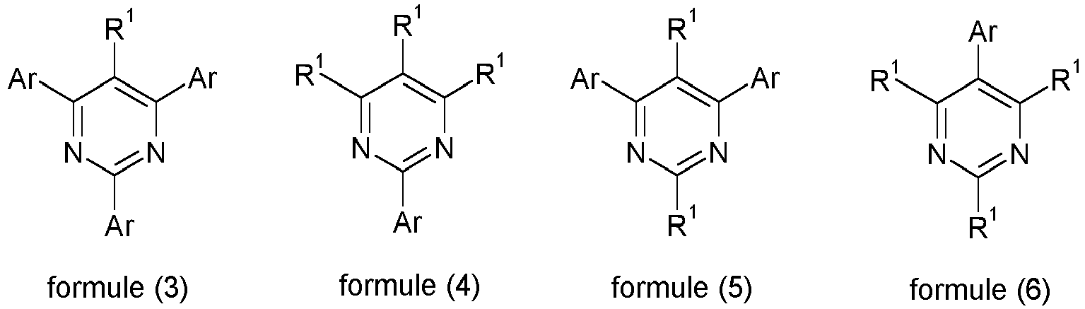
- the compounds of the following formula (39) or (40) are particularly suitable here, where the symbols used have the meanings given above.
- Examples of suitable carbazole derivatives are the compounds (1) to (11) shown in the table below. (1) (2) (3) (4) (5) (6) (7) (8th) (9) (10) (11)
- the material ETM2 is a diazasilole derivative or a tetraazasilole derivative, e.g. B. according WO 2010/054729 .
- the organic electroluminescent device can also contain further layers. These are selected, for example, from one or more hole injection layers, hole transport layers, further electron transport layers, electron injection layers, electron blocking layers, exciton blocking layers, charge generation layers (charge generation layers) and / or organic or inorganic p / n transitions. You can also use intermediate layers be present, in particular as an intermediate layer between a fluorescent and a phosphorescent layer. Furthermore, the layers, in particular the charge transport layers, can also be doped. The doping of the layers can be advantageous for improved charge transport.
- each of the layers mentioned above does not necessarily have to be present and the choice of layers always depends on the compounds used.
- the use of such layers is known to the person skilled in the art and he can use all materials known for such layers according to the prior art for this purpose without inventive step.
- it is a white-emitting organic electroluminescent device. This is characterized by the fact that it emits light with CIE color coordinates in the range from 0.28 / 0.29 to 0.45 / 0.41.
- the general structure of such a white-emitting electroluminescent device is shown, for example, in WO 2005/011013 disclosed.
- Metals with a low work function, metal alloys or multilayer structures made of different metals are preferred as the cathode of the electroluminescent device according to the invention, such as, for example, alkaline earth metals, alkali metals, main group metals or lanthanoids (e.g. Ca, Ba, Mg, Al, In, Mg, Yb, Sm, Etc.).
- alkaline earth metals alkali metals
- main group metals or lanthanoids e.g. Ca, Ba, Mg, Al, In, Mg, Yb, Sm, Etc.
- other metals can also be used in addition to the metals mentioned, which have a relatively high work function, such as, for example, B. Ag, in which case combinations of the metals, such as Mg / Ag, Ca / Ag or Ba / Ag are usually used.
- Metal alloys are also preferred, in particular alloys made of an alkali metal or alkaline earth metal and silver, particularly preferably an alloy of Mg and Ag. It may also be preferred to insert a thin intermediate layer of a material with a high dielectric constant between a metallic cathode and the organic semiconductor.
- alkali metal or alkaline earth metal fluorides for this purpose come, for example, alkali metal or alkaline earth metal fluorides, but also the corresponding oxides or carbonates (e.g. LiF, Li 2 O, Li 3 N, CsF, RbF, Cs 2 CO 3 , BaF 2 , MgO, NaF, etc.) or Metal complexes (e.g. lithium hydroxyquinolinate) in question.
- the layer thickness of this layer is preferably between 0.5 and 5 nm.
- an electron injection layer is used between the metallic cathode and the electron transport layer according to the invention, the electron injection layer preferably containing one of the materials mentioned above.
- the anode preferably has a work function greater than 4.5 eV vs. Vacuum on. Metals with a high redox potential, such as Ag, Pt or Au, are suitable for this.
- metal / metal oxide electrodes e.g. Al / Ni / NiO x , Al / PtO x
- At least one of the electrodes must be transparent or partially transparent to enable light to be coupled out.
- Preferred anode materials for transparent or partially transparent anodes are conductive mixed metal oxides. Indium tin oxide (ITO) or indium zinc oxide (IZO) are particularly preferred.
- the device is structured accordingly (depending on the application), contacted and finally hermetically sealed, since the life of such devices is drastically shortened in the presence of water and / or air.
- the emitting layer can be phosphorescent or fluorescent. It is also possible for both a fluorescent and a phosphorescent emitter layer to be present.
- the emitting layer is a fluorescent layer, in particular a blue or green fluorescent layer.
- Preferred dopants which can be used in the fluorescent emitter layer are selected from the class of the monostyrylamines, the distyrylamines, the tristyrylamines, the tetrastyrylamines and the arylamines.
- a monostyrylamine is understood to mean a compound which contains a substituted or unsubstituted styryl group and at least one, preferably aromatic, amine.
- a distyrylamine is understood to mean a compound which contains two substituted or unsubstituted styryl groups and at least one, preferably aromatic, amine.
- a tristyrylamine is understood to mean a compound which contains three substituted or unsubstituted styryl groups and at least one, preferably aromatic, amine.
- a tetrastyrylamine is understood to mean a compound which contains four substituted or unsubstituted styryl groups and at least one, preferably aromatic, amine.
- the styryl groups are particularly preferred stilbenes, which can also be further substituted.
- An arylamine or an aromatic amine in the sense of this invention is taken to mean a compound which contains three substituted or unsubstituted aromatic or heteroaromatic ring systems bonded directly to the nitrogen.
- At least one of these aromatic or heteroaromatic ring systems is preferably a condensed ring system, particularly preferably with at least 14 aromatic ring atoms.
- Preferred examples of this are aromatic anthracenamines, aromatic anthracene diamines, aromatic pyrenamines, aromatic pyrendiamines, aromatic chrysenamines or aromatic chrysediamines.
- An aromatic anthracenamine is understood to mean a compound in which a diarylamino group is bonded directly to an anthracene group, preferably in the 2- or 9-position.
- aromatic anthracene diamine is understood to mean a compound in which two diarylamino groups are directly connected to an anthracene group are bound, preferably in the 2,6- or 9,10-position.
- Aromatic pyrenamines, pyrendiamines, chrysenamines and chrysendiamines are defined analogously, the diarylamino groups being preferably attached to the pyrene in the 1-position or in the 1,6-position.
- fluorescent dopants are selected from indenofluorenamines or diamines, for example according to WO 2006/122630 , Benzoindenofluorenaminen or diamines, for example according to WO 2008/006449 , and Dibenzoindenofluorenaminen or diamines, for example according to WO 2007/140847 .
- Examples of dopants from the class of the styrylamines are substituted or unsubstituted tristilbenamines or the dopants which are described in WO 2006/000388 , WO 2006/058737 , WO 2006/000389 , WO 2007/065549 and WO 2007/115610 are described.
- fluorescent dopants are condensed aromatic hydrocarbons, such as those in WO 2010/012328 disclosed compounds. These preferably have no arylamino groups. Particularly preferred fluorescent dopants are the aromatic hydrocarbons listed above WO 2010/012328 which have no arylamino groups and aromatic amines which contain at least one fused aromatic group having at least 14 aromatic ring atoms, and fused aromatic hydrocarbons.
- Suitable host materials (matrix materials) for the fluorescent dopant are selected, for example, from the classes of the oligoarylenes (for example 2,2 ', 7,7'-tetraphenylspirobifluorene according to EP 676461 or dinaphthylanthracene), especially the oligoarylenes containing condensed aromatic groups, the polypodal metal complexes (e.g. according to WO 2004/081017 ), the electron-conducting compounds, in particular ketones, phosphine oxides, sulfoxides, etc. (e.g.
- the atropisomers e.g. according to WO 2006/048268
- the boronic acid derivatives e.g. according to WO 2006/117052
- the benzanthracene derivatives e.g. benz- [a] anthracene derivatives according to WO 2008/145239 or according to the undisclosed application DE 102009034625.2
- the benzophenanthrene derivatives e.g. benz [c] phenanthrene derivatives according to WO 2010/083869 ).
- Particularly preferred host materials are selected from the classes of oligoarylenes containing naphthalene, anthracene, benzanthracene, especially benz [a] anthracene, benzophenanthrene, especially benz [c] phenanthrene, and / or pyrene.
- An oligoarylene in the sense of this invention is to be understood as a compound in which at least three aryl or arylene groups are bonded to one another.
- At least one of the groups Ar 4 contains a condensed aryl group with 10 or more aromatic ring atoms, it being possible for Ar 4 to be substituted by one or more radicals R 1 .
- Preferred groups Ar 4 are the same or different at each occurrence selected from the group consisting of phenyl, 1-naphthyl, 2-naphthyl, anthracenyl, ortho-, meta- or para-biphenyl, phenylene-1-naphthyl, phenylene-2-naphthyl , Phenanthrenyl, benz [a] anthracenyl, benz [c] phenanthrenyl or combinations of two or three of these groups, which can each be substituted by one or more radicals R 1 .
- the emitting layer contains a phosphorescent emitter.
- Phosphorescence in the sense of this invention means luminescence from an excited state with spin multiplicity> 1, in particular from an excited triplet state.
- all luminescent transition metal complexes with transition metals of the second and third transition metal series in particular all luminescent iridium, platinum and copper compounds, are to be regarded as phosphorescent compounds.
- the phosphorescent compound is a red phosphorescent compound or a green phosphorescent compound.
- Suitable phosphorescent compounds are, in particular, compounds which, when suitably excited, emit light, preferably in the visible range, and additionally contain at least one atom of atomic number greater than 20, preferably greater than 38 and less than 84, particularly preferably greater than 56 and less than 80.
- Compounds which contain copper, molybdenum, tungsten, rhenium, ruthenium, osmium, rhodium, iridium, palladium, platinum, silver, gold or europium are preferably used as phosphorescence emitters, in particular compounds which contain iridium, platinum or copper.
- Suitable matrix materials for the compounds according to the invention are ketones, phosphine oxides, sulfoxides and sulfones, e.g. B. according WO 2004/013080 , WO 2004/093207 , WO 2006/005627 or WO 2010/006680 , Triarylamines, carbazole derivatives, e.g. B.
- CBP N, N-bis-carbazolylbiphenyl
- m-CBP in WO 2005/039246 , US 2005/0069729 , JP 2004/288381 , EP 1205527 , WO 2008/086851 or US 2009/0134784 disclosed carbazole derivatives, indolocarbazole derivatives, e.g. B. according WO 2007/063754 or WO 2008/056746 , Indenocarbazole derivatives, e.g. B. according WO 2010/136109 or WO 2011/000455 , Azacarbazoles, e.g. B.
- Zinc complexes e.g. B. according EP 652273 or WO 2009/062578
- Dibenzofuran derivatives e.g. B. according WO 2009/148015
- bridged carbazole derivatives e.g. B. according US 2009/0136779 , WO 2010/050778 , WO 2011/042107 , WO 2011/060867 or DE 102010005697 .
- a preferred combination is, for example, the use of an aromatic ketone or a triazine derivative with a triarylamine derivative or a carbazole derivative as a mixed matrix.
- Also preferred is the use of a mixture of a charge-transporting matrix material and an electrically inert matrix material, which is not or not significantly involved in the charge transport, such as. B. in WO 2010/108579 described.
- the use of a mixture of two or more matrix materials, in particular of a hole-conducting and an electron-conducting matrix material, in combination with the electron transport layer according to the invention is a preferred embodiment of the invention.
- Suitable charge transport materials such as can be used in the hole injection or hole transport layer or in the electron transport layer of the organic electroluminescent device according to the invention are, for example, those in Y. Shirota et al., Chem. Rev. 2007, 107 (4), 953-1010 disclosed compounds or other materials as are used in these layers according to the prior art.
- Examples of preferred hole transport materials which can be used in a hole transport or hole injection layer in the electroluminescent device according to the invention are indenofluorenamines and derivatives (e.g. according to WO 2006/122630 or WO 2006/100896 ), in the EP 1661888 disclosed amine derivatives, hexaazatriphenylene derivatives (e.g. according to WO 2001/049806 ), Amine derivatives with condensed aromatics (e.g. according to US 5,061,569 ), in the WO 95/09147 disclosed amine derivatives, monobenzoindenofluorenamines (e.g. according to WO 2008/006449 ) or dibenzoindenofluorenamines (e.g.
- the organic electroluminescent device according to the invention can be manufactured by various methods. Another object of the present invention is therefore a method for producing an organic electroluminescent device, as explained below.
- An organic electroluminescent device is preferred, characterized in that one or more layers are coated using a sublimation process.
- the materials are evaporated in vacuum sublimation systems at an initial pressure of less than 10 -5 mbar, preferably less than 10 -6 mbar. However, it should be noted that the initial pressure can also be lower, for example less than 10 -7 mbar.
- An organic electroluminescent device is also preferred, characterized in that one or more layers are coated with the OVPD (Organic Vapor Phase Deposition) process or with the aid of a carrier gas sublimation.
- the materials are applied at a pressure between 10 -5 mbar and 1 bar.
- OVJP Organic Vapor Jet Printing
- the materials are applied directly through a nozzle and structured (e.g. BMS Arnold et al., Appl. Phys. Lett. 2008, 92, 053301 ).
- an organic electroluminescent device characterized in that one or more layers of solution, such as. B. by spin coating, or with any printing method, such as. B. screen printing, flexographic printing, offset printing, LITI (Light Induced Thermal Imaging, thermal transfer printing), ink jet printing (ink jet printing) or nozzle printing can be produced. Soluble connections are necessary for this. High solubility can be achieved by suitable substitution of the compounds. Not only can solutions made of individual materials be applied, but also solutions that contain several compounds, for example matrix materials and dopants.
- the organic electroluminescent device can also be produced as a hybrid system in that one or more layers of solution are applied and one or more further layers are vapor-deposited.
- one or more layers of solution are applied and one or more further layers are vapor-deposited.
- the organic electroluminescent device can be used for various applications, in particular for display applications or as a light source, for example for lighting applications or for medical applications.
- the HOMO and LUMO layers as well as the triplet level of the materials are determined using quantum chemical calculations.
- the program package "Gaussian03W” (Gaussian Inc.) is used for this.
- To calculate organic substances without metals (referred to in Table 4 with the "org.” Method), geometry optimization is first carried out using the "Ground State / Semi-empirical / Default Spin / AM1 / Charge O / Spin Singlet” method. This is followed by an energy calculation based on the optimized geometry.
- the "TD-SFC / DFT / Default Spin / B3PW91” method is used here with the base set “6-31G (d)" (batch 0, spin singlet).
- HOMO or LUMO of the materials are to be regarded as HOMO or LUMO of the materials.
- a HOMO of -0.19767 Hartrees and a LUMO of - 0.04783 Hartrees are obtained for the substance ETM2-2, which corresponds to a calibrated HOMO of -5.68346 eV and a calibrated LUMO of -2.38675 eV.
- the triplet level T 1 is defined as the energy of the triplet state with the lowest energy, which results from the quantum chemical calculation.
- Table 6 shows the HOMO and LUMO values as well as the triplet levels T 1 of the different materials.
- OLEDs and OLEDs according to the prior art are produced by a general process according to WO 2004/058911 , which is adapted to the conditions described here (layer thickness variation, materials).
- the following examples show the data from different OLEDs.
- Glass substrates coated with structured ITO (indium tin oxide) with a thickness of 50 nm are cleaned intensively with an alkaline detergent and then rinsed 3 times with deionized water. After drying and heating these substrates, they are pretreated with an oxygen plasma for 5 minutes and then immediately coated with OLED materials in a vacuum chamber.
- the OLEDs basically have the following layer structure: substrate / hole injection layers (HIL) / hole transport layers (HTL) / emission layer (EML) / electron transport layers (ETL) / optional electron injection layer (EIL) and finally a cathode.
- the cathode is formed by a 100 nm thick aluminum layer.
- the exact structure of the OLEDs can be found in Table 1.
- Table 5 The materials required to manufacture the OLEDs are shown in Table 5.
- the emission layer always consists of at least one matrix material (host material, host material) and an emitting dopant (dopant, emitter), which is admixed to the matrix material or the matrix materials by cover vaporization in a certain volume fraction.
- An indication such as M1 (95%): D1 (5%) means that the material M1 is present in the layer in a volume fraction of 95% and D1 in a volume fraction of 5%.
- the object of the invention is that a mixture of at least two materials, such as ETM1-1 (50%): ETM2-1 (50%), is also present in the electron transport layer.
- the OLEDs are characterized by default.
- the electroluminescence spectra, the current efficiency (measured in cd / A) as a function of the luminance, calculated from current-voltage-luminance characteristics (IUL characteristics), and the service life are determined.
- the electroluminescence spectra are measured at a luminance of 1000 cd / m 2 , which gives the CIE 1931 x and y color coordinates.
- the specification U1000 in table 2 denotes the voltage required for a luminance of 1000 cd / m 2 .
- SE1000 denotes the current efficiency that can be achieved at 1000 cd / m 2 .
- the values for the service life can be converted to a specification for other starting luminance values using conversion formulas known to the person skilled in the art.
- the service life for a starting luminance of 1000 cd / m 2 is a common specification.
- Examples A1-A15 and A16-A19 are comparative examples according to the prior art, examples B1-B9 and B10 to B20 show data from OLEDs with materials or material combinations according to the invention.
- OLEDs with electron transport layers according to the invention containing ETM1 and ETM2
- the OLEDs A1-A4 are comparative examples which contain no ETM2 materials in the electron transport layer adjacent to the emitter layer, but only an ETM material (ETM1-1).
- ETM2-1 which is often used as an admixture according to the prior art, is used here as an EIL in a separate layer.
- Table 2 it can be seen that by optimizing the layer thickness of the ETM2-1 used as a single layer, no further optimization of the component is possible. The voltages, efficiencies and lifetimes of the components are all very similar. From a layer thickness of 4 nm ETM2-1, however, the service life drops significantly.
- the OLEDs A5-A8 are comparative examples which contain a mixture of ETM1 and ETM2 (ETM1-1 and ETM2-1), which do not correspond to the invention, in the electron transport layer adjacent to the emitter layer, according to the prior art.
- ETM2-1 is also used in a separate electron injection layer.
- Table 2 it can be seen that a mixture of ETM1-1 and ETM2-1 compared to Examples A1-A4 already optimizes the component in terms of voltage (reductions of approx. -1V) and efficiency (increases of up to 60 %) is possible.
- the OLEDs A9-A12 are comparative examples which, in the electron transport layer adjacent to the emitter layer, a mixture of ETM1, which corresponds to the triplet level of the present invention, and ETM2, which does not correspond to the triplet level of the present invention (ETM1- 2 and ETM2-1).
- ETM1- 2 and ETM2-1 blue devices (fluorescent emitters)
- ETM2-1 is also used here in a separate EIL.
- the OLEDs B1-B4 are examples according to the invention which contain a mixture of ETM1 and ETM2 (ETM1-2 and ETM2-2) according to the present invention in the electron transport layer adjacent to the emitter layer.
- ETM2-1 is used here in a separate electron injection layer.
- Table 2 it can be seen that a suitable mixture of ETM1-2 and ETM2-2 compared to Examples A9-A12 further optimizes the component in terms of efficiency (increases of approx. 5%) and service life (extensions of up to 45%) is possible.
- the compatibility with phosphorescent layers is given here.
- the OLEDs A13-A15 are green comparative examples which, in the electron transport layer adjacent to the emitter layer, contain a mixture of two ETMs not according to the invention or from one ETM according to the invention and one not according to the invention (ETM1-1: ETM2-1, ETM1-1: ETM2-3 or ETM1 -3: ETM2-1) included. In this case, one of the components does not meet the triplet level requirements. For example, while the combination ETM1-1: ETM2-1 from comparative examples A5 to A8 in singlet blue still worked relatively well, the efficiency in triplet green (A13) is low.
- examples B5-B9 according to the invention only contain electron transport materials in the ETM layer (ETM1-3: ETM2-3) which meet all of the conditions according to the invention.
- the mutagenic ETM2-1 is used in a separate electron injection layer.
- Examples B6-B9 therefore use other, less harmful electron injection materials, such as cesium fluoride, lithium nitride, rubidium fluoride or lithium fluoride, which, except in the case of lithium fluoride, do not lead to any noteworthy change in the device performance compared to B5.
- the OLEDs A16-A19 in Table 3 are comparative examples which contain a mixture in the electron transport layer adjacent to the emitter layer which does not meet the conditions according to the invention.
- B10 to B20 are examples according to the invention.
- the evaluation data are summarized in Table 4.
- B11 the mutagenic ETM2-1 was replaced by the less harmful electron injection material cesium fluoride, which did not lead to any noteworthy change in device performance compared to B10.
- the replacement of ETM2-1 is therefore possible without loss of performance, which is a great advantage in the end product (recycling cycle, environmental and health assessment), but also in terms of production safety.
- Examples B10 to B20 according to the invention from Table 4 show that by means of a mixture of electron transport materials according to the invention in comparison with the components which contain no or not only electron transport materials according to the invention, an optimization of the component with regard to voltage (reductions of up to -0.2 V), Efficiency (increases of over 30%) and lifespan (extensions of over 18%) is possible.
- the improvement is particularly pronounced with these phosphorescent components, which have a mixed matrix of two matrix materials in the emitting layer, since here the emission zone is particularly strongly shifted to the ETL side and the effects of a small T1 level in the Impact ETL particularly strongly.
- Table 5 shows all chemical structures used in the examples.
- Table 3 shows the structure of OLEDs A16 to A19 and B10 to B20. There is always 50 nm of ITO in front of the first layer, and 100 nm of aluminum is always evaporated onto the last ETM layer; the individual layers are separated from each other in the table by "/", the layer thicknesses in parentheses in nm.
- the OLEDs listed here have the following layer structure: HIM2 (40) / HIM1 (10) / HIM2 (170) / HIM1 (10) / HTM3 (20) / M3 (32%): M4 (63%) D3 (5%) (40) / ETMX / ETMY ⁇ b> Table 3 ⁇ /b> E.g. no.
Landscapes
- Physics & Mathematics (AREA)
- Engineering & Computer Science (AREA)
- Chemical & Material Sciences (AREA)
- Optics & Photonics (AREA)
- Manufacturing & Machinery (AREA)
- Organic Chemistry (AREA)
- Spectroscopy & Molecular Physics (AREA)
- Materials Engineering (AREA)
- Electroluminescent Light Sources (AREA)
Claims (15)
- Dispositif électroluminescent organique comprenant une anode, une cathode, au moins une couche d'émission et au moins une couche de transport d'électrons qui est directement adjacente à la couche d'émission sur le côté de cathode, caractérisé en ce que la couche de transport d'électrons comprend un mélange d'au moins deux matériaux ETM1 et ETM2, où les conditions qui suivent s'appliquent au ETM1 et au ETM2 :a) T1(ETM1) > 2,2 eV ; etb) T1(ETM2) > 2,2 eV ; etc) -3,2 eV < LUMO(ETM1) < -2,0 eV ; etd) LUMO(ETM2) > LUMO(ETM1) ;où T1 représente l'énergie de triplet la plus faible du matériau respectif et LUMO représente l'énergie de l'orbite moléculaire non occupée la plus basse du matériau respectif ; et
où le ETM1 et le ETM2 sont des matériaux purement organiques,
et où les énergies de triplet et les valeurs de la HOMO et de la LUMO sont déterminées en utilisant le procédé de la théorie fonctionnelle de la densité en fonction du temps qui est divulgué dans la section des exemples. - Dispositif électroluminescent organique selon la revendication 1, caractérisé en ce que l'énergie de triplet T1 du ETM1 et du ETM2 et de quelconques autres matériaux qui sont présents dans la couche de transport d'électrons est > 2,4 eV, de préférence, est > 2,6 eV.
- Dispositif électroluminescent organique selon la revendication 1 ou 2, caractérisé en ce que la LUMO du ETM1 s'inscrit à l'intérieur de la plage qui va de -3,1 eV à -2,2 eV de préférence, à l'intérieur de la plage qui va de -3,0 eV à -2,4 eV.
- Dispositif électroluminescent organique selon une ou plusieurs des revendications 1 à 3, caractérisé en ce que la LUMO du ETM2 est d'au moins 0,1 eV plus grande que la LUMO du ETM1.
- Dispositif électroluminescent organique selon une ou plusieurs des revendications 1 à 4, caractérisé en ce que la HOMO du ETM1 est < -5,3 eV.
- Dispositif électroluminescent organique selon une ou plusieurs des revendications 1 à 5, caractérisé en ce que HOMO(ETM1) < HOMO(EML) et HOMO(ETM2) < HOMO(EML), où HOMO(EML) représente la HOMO de la couche d'émission ou du matériau de la couche d'émission qui présente la HOMO la plus haute.
- Dispositif électroluminescent organique selon une ou plusieurs des revendications 1 à 6, caractérisé en ce que la proportion du ETM2 est ≥ 10 % en vol. et de préférence, est ≥ 30 % en vol. et en outre, la proportion du ETM2 est ≤ 90 % en vol. et de préférence, est ≤ 80 % en vol.
- Dispositif électroluminescent organique selon une ou plusieurs des revendications 1 à 7, caractérisé en ce que la couche de transport d'électrons ne comprend pas d'autres matériaux en dehors du ETM1 et du ETM2.
- Dispositif électroluminescent organique selon une ou plusieurs des revendications 1 à 8, caractérisé en ce que le ETM1 est sélectionné parmi le groupe qui est constitué par les composés qui contiennent des groupes de cycle hétéroaryle à six éléments, en particulier les dérivés de triazine, les dérivés de pyrimidine, les dérivés de pyridine, les dérivés de pyrazine, les dérivés de quinoxaline ou les dérivés de quinoline, les composés qui contiennent des groupes de cycle hétéroaromatique à cinq éléments qui comportent au moins deux hétéroatomes, en particulier les dérivés d'oxadiazole ou les dérivés de benzimidazole, ou par les cétones aromatiques, les boranes aromatiques, les lactames aromatiques, les dérivés de diazaphosphole et les dérivés d'oxyde de phosphine.
- Dispositif électroluminescent organique selon une ou plusieurs des revendications 1 à 9, caractérisé en ce que le ETM1 qui est utilisé est un composé de l'une des formules (1) à (8),

 Ar est, de manière identique ou différente pour chaque occurrence, un système de cycle aromatique ou hétéroaromatique monovalent qui comporte de 5 à 60 atomes de cycle aromatique, lequel peut dans chaque cas être substitué par un radical ou par plusieurs radicaux R1 ;Ar1 est un système de cycle aromatique ou hétéroaromatique divalent qui comporte de 5 à 60 atomes de cycle aromatique, lequel peut être substitué par un radical ou par plusieurs radicaux R1 ;R1 est pour chaque occurrence, de manière identique ou différente, H, D, F, Cl, Br, I, CHO, C(=O)Ar2, P(=O)(Ar2)2, S(=O)Ar2, S(=O)2Ar2, CR2=CR2Ar2, CN, NO2, Si(R2)3, B(OR2)2, B(R2)2, B(N(R2)2)2, OSO2R2, un groupe alkyle, alcoxy ou thioalcoxy en chaîne droite qui comporte de 1 à 40 atome(s) de C ou un groupe alkényle ou alkynyle en chaîne droite qui comporte de 2 à 40 atomes de C ou un groupe alkyle, alkényle, alkynyle, alcoxy ou thioalcoxy ramifié ou cyclique qui comporte de 3 à 40 atomes de C, lequel peut dans chaque cas être substitué par un radical ou par plusieurs radicaux R2, où un ou plusieurs groupe(s) CH2 non adjacents peut/peuvent être remplacé(s) par R2C=CR2, C=C , Si(R2)2, Ge(R2)2, Sn(R2)2, C=O, C=S, C=Se, C=NR2, P(=O)(R2), SO, SO2, NR2, O, S ou CONR2 et où un ou plusieurs atome(s) de H peut/peuvent être remplacé(s) par F, Cl, Br, I, CN ou NO2, ou un système de cycle aromatique ou hétéroaromatique qui comporte de 5 à 60 atomes de cycle aromatique, lequel peut dans chaque cas être substitué par un radical ou par plusieurs radicaux R2, ou un groupe aryloxy ou hétéroaryloxy qui comporte de 5 à 60 atomes de cycle aromatique, lequel peut être substitué par un radical ou par plusieurs radicaux R2, ou une combinaison de ces systèmes ; deux substituants R1 adjacents ou plus peuvent également former un système de cycle aliphatique ou aromatique mono- ou polycyclique l'un avec l'autre ou les uns avec les autres ;Ar2 est pour chaque occurrence, de manière identique ou différente, un système de cycle aromatique ou hétéroaromatique qui comporte de 5 à 40 atomes de cycle aromatique, lequel peut être substitué par un radical ou par plusieurs radicaux R2 ;R2 est pour chaque occurrence, de manière identique ou différente, H, D, CN ou un radical organique aliphatique, aromatique et/ou hétéroaromatique qui comporte de 1 à 20 atome(s) de C, où, en outre, des atomes de H peuvent être remplacés par F ; deux substituants R2 adjacents ou plus peuvent également former un système de cycle aliphatique ou aromatique mono- or polycyclique l'un avec l'autre ou les uns avec les autres ;ou caractérisé en ce que le ETM1 qui est utilisé est un cétone de la formule (23) ou un oxyde de phosphine de la formule (24),
- Dispositif électroluminescent organique selon une ou plusieurs des revendications 1 à 10, caractérisé en ce que le ETM2 est un hydrocarbone pur, de préférence un hydrocarbone aromatique, ou en ce que le ETM2 est un dérivé de carbazole, un dérivé de diazasilole ou un dérivé de tétraazasilole.
- Dispositif électroluminescent organique selon une ou plusieurs des revendications 1 à 11, caractérisé en ce que le ETM2 est sélectionné parmi les composés des formules (36), (37) et (38),
 Ar3 est pour chaque occurrence, de manière identique ou différente, un système de cycle aromatique qui comporte de 6 à 60 atomes de C aromatique, lequel ne contient pas de groupes non aromatiques autres que carbone ou hydrogène ; Ar3 peut être substitué par un radical ou par plusieurs radicaux R4 ;R3 est pour chaque occurrence, de manière identique ou différente, un groupe alkyle en chaîne droite qui comporte de 1 à 20 atome(s) de C ou un groupe alkyle ramifié ou cyclique qui comporte de 3 à 20 atomes de C, ou un système de cycle aromatique qui comporte de 6 à 60 atomes de C aromatique, lequel ne contient pas de groupes non aromatiques autres que carbone ou hydrogène et lequel peut être substitué par un radical ou par plusieurs radicaux R4 ; deux radicaux R3 ou plus peuvent également former un système de cycle l'un avec l'autre ou les uns avec les autres ;R4 est pour chaque occurrence, de manière identique ou différente, un groupe alkyle en chaîne droite qui comporte de 1 à 20 atome(s) de C ou un groupe alkyle ramifié ou cyclique qui comporte de 3 à 20 atomes de C ; deux radicaux R4 ou plus peuvent également former un système de cycle l'un avec l'autre ou les uns avec les autres ;n est, de manière identique ou différente pour chaque occurrence, 0 ou 1 ;ou caractérisé en ce que le ETM2 qui est utilisé est un composé de la formule (39) ou (40) :
- Dispositif électroluminescent organique selon une ou plusieurs des revendications 1 à 12, caractérisé en ce qu'une couche d'injection d'électrons qui comprend un fluorure de métal alcalin ou un fluorure de métal alcalino-terreux, un oxyde de métal alcalin ou un oxyde de métal alcalino-terreux, un carbonate de métal alcalin ou un carbonate de métal alcalino-terreux ou un complexe de métal alcalin ou un complexe de métal alcalino-terreux est utilisée entre la couche de transport d'électrons et la cathode métallique.
- Dispositif électroluminescent organique selon une ou plusieurs des revendications 1 à 13, caractérisé en ce que la couche d'émission est phosphorescente et de préférence, elle comprend un mélange de deux matériaux de matrice ou plus.
- Procédé pour la fabrication d'un dispositif électroluminescent organique selon une ou plusieurs des revendications 1 à 14, caractérisé en ce qu'une ou plusieurs couche(s) est/sont appliquée(s) au moyen d'un processus de sublimation et/ou en ce qu'une ou plusieurs couche(s) est/sont appliquée(s) au moyen d'un processus OVPD ou à l'aide d'une sublimation par gaz porteur et/ou en ce qu'une ou plusieurs couche(s) est/sont appliquée(s) à partir d'une solution.
Priority Applications (1)
| Application Number | Priority Date | Filing Date | Title |
|---|---|---|---|
| EP12740070.3A EP2748878B1 (fr) | 2011-08-22 | 2012-07-25 | Dispositif électroluminescent organique |
Applications Claiming Priority (3)
| Application Number | Priority Date | Filing Date | Title |
|---|---|---|---|
| EP11006859 | 2011-08-22 | ||
| PCT/EP2012/003152 WO2013026515A1 (fr) | 2011-08-22 | 2012-07-25 | Dispositif électroluminescent organique |
| EP12740070.3A EP2748878B1 (fr) | 2011-08-22 | 2012-07-25 | Dispositif électroluminescent organique |
Publications (2)
| Publication Number | Publication Date |
|---|---|
| EP2748878A1 EP2748878A1 (fr) | 2014-07-02 |
| EP2748878B1 true EP2748878B1 (fr) | 2020-04-01 |
Family
ID=46581906
Family Applications (1)
| Application Number | Title | Priority Date | Filing Date |
|---|---|---|---|
| EP12740070.3A Active EP2748878B1 (fr) | 2011-08-22 | 2012-07-25 | Dispositif électroluminescent organique |
Country Status (6)
| Country | Link |
|---|---|
| US (2) | US9735385B2 (fr) |
| EP (1) | EP2748878B1 (fr) |
| JP (1) | JP6203720B2 (fr) |
| KR (2) | KR102051790B1 (fr) |
| CN (1) | CN103765623B (fr) |
| WO (1) | WO2013026515A1 (fr) |
Families Citing this family (29)
| Publication number | Priority date | Publication date | Assignee | Title |
|---|---|---|---|---|
| CN102869672B (zh) * | 2010-05-03 | 2016-05-11 | 默克专利有限公司 | 制剂和电子器件 |
| KR101778825B1 (ko) | 2010-05-03 | 2017-09-14 | 메르크 파텐트 게엠베하 | 제형물 및 전자 소자 |
| DE102010045405A1 (de) * | 2010-09-15 | 2012-03-15 | Merck Patent Gmbh | Materialien für organische Elektrolumineszenzvorrichtungen |
| JP6553022B2 (ja) * | 2013-04-08 | 2019-07-31 | メルク パテント ゲーエムベーハー | 有機エレクトロルミネッセント素子 |
| KR102188028B1 (ko) * | 2013-06-18 | 2020-12-08 | 삼성디스플레이 주식회사 | 유기 발광 소자 |
| JP2015005747A (ja) * | 2013-06-21 | 2015-01-08 | ダウ グローバル テクノロジーズ エルエルシー | トリアジンから得られる化合物を含有する薄膜およびそこから形成される電子デバイス |
| KR102079254B1 (ko) * | 2013-06-24 | 2020-02-20 | 삼성디스플레이 주식회사 | 유기 발광 소자 |
| EP2887416B1 (fr) * | 2013-12-23 | 2018-02-21 | Novaled GmbH | Matériau semi-conducteur dopé N comprenant une matrice d'oxyde de phosphine et un dopant de métal |
| KR101537500B1 (ko) * | 2014-04-04 | 2015-07-20 | 주식회사 엘지화학 | 유기 발광 소자 |
| EP3663289A1 (fr) * | 2014-06-11 | 2020-06-10 | Hodogaya Chemical Co., Ltd. | Dérivés de pyrimidine et dispositifs organiques électroluminescents |
| KR102273047B1 (ko) * | 2014-06-30 | 2021-07-06 | 삼성디스플레이 주식회사 | 유기 발광 소자 |
| EP2963696A1 (fr) * | 2014-07-04 | 2016-01-06 | Novaled GmbH | Diode électroluminescente organique (OLED) comprenant un empilement de couches de transport d'électrons comprenant différents composés de lithium |
| US10297762B2 (en) * | 2014-07-09 | 2019-05-21 | Universal Display Corporation | Organic electroluminescent materials and devices |
| WO2016068585A1 (fr) * | 2014-10-27 | 2016-05-06 | 주식회사 엘지화학 | Dispositif électroluminescent organique |
| KR102611317B1 (ko) * | 2014-12-24 | 2023-12-07 | 솔루스첨단소재 주식회사 | 유기 화합물 및 이를 포함하는 유기 전계 발광 소자 |
| EP3259330B1 (fr) * | 2015-02-16 | 2018-11-14 | Merck Patent GmbH | Matériaux à base de dérivés de spirobifluorène pour dispositifs électroniques |
| EP3093288A1 (fr) * | 2015-05-12 | 2016-11-16 | Novaled GmbH | Diode électroluminescente organique comprenant différents composés matriciels dans la première et la seconde couche de transport d'électrons |
| EP3147961A1 (fr) * | 2015-09-28 | 2017-03-29 | Novaled GmbH | Dispositif électroluminescent organique |
| EP3208861A1 (fr) * | 2016-02-19 | 2017-08-23 | Novaled GmbH | Couche de transport d'électrons comprenant un mélange composé de matrice pour une diode électroluminescente organique (oled) |
| JP6815294B2 (ja) | 2016-09-30 | 2021-01-20 | 株式会社Joled | 有機el素子、および有機elパネル |
| CN109791982B (zh) * | 2016-11-23 | 2023-10-17 | 广州华睿光电材料有限公司 | 有机混合物、有机组合物、有机电子器件及其制备方法 |
| KR20190070586A (ko) * | 2017-12-13 | 2019-06-21 | 엘지디스플레이 주식회사 | 전자수송 재료용 화합물 및 이를 포함하는 유기 발광 다이오드 |
| TWI713848B (zh) * | 2018-05-18 | 2020-12-21 | 國立交通大學 | 有機發光元件 |
| CN110556483A (zh) * | 2018-06-04 | 2019-12-10 | Tcl集团股份有限公司 | 电致发光器件及其制备方法和应用 |
| CN110600623B (zh) * | 2018-06-13 | 2021-08-27 | Tcl科技集团股份有限公司 | 电致发光器件及其制备方法 |
| WO2020067823A1 (fr) | 2018-09-28 | 2020-04-02 | 주식회사 엘지화학 | Élément électroluminescent organique |
| WO2020109269A1 (fr) * | 2018-11-29 | 2020-06-04 | Merck Patent Gmbh | Dispositif électronique |
| JP2020191442A (ja) * | 2019-05-17 | 2020-11-26 | 学校法人関西学院 | 有機電界発光素子 |
| CN116574131A (zh) * | 2022-12-08 | 2023-08-11 | 四川阿格瑞新材料有限公司 | 一种电子传输材料及其在电致发光器件中的应用 |
Family Cites Families (79)
| Publication number | Priority date | Publication date | Assignee | Title |
|---|---|---|---|---|
| US4539507A (en) | 1983-03-25 | 1985-09-03 | Eastman Kodak Company | Organic electroluminescent devices having improved power conversion efficiencies |
| US4780536A (en) | 1986-09-05 | 1988-10-25 | The Ohio State University Research Foundation | Hexaazatriphenylene hexanitrile and its derivatives and their preparations |
| US5061569A (en) | 1990-07-26 | 1991-10-29 | Eastman Kodak Company | Electroluminescent device with organic electroluminescent medium |
| US5151629A (en) | 1991-08-01 | 1992-09-29 | Eastman Kodak Company | Blue emitting internal junction organic electroluminescent device (I) |
| JP3295088B2 (ja) | 1993-09-29 | 2002-06-24 | 出光興産株式会社 | 有機エレクトロルミネッセンス素子 |
| DE69412567T2 (de) | 1993-11-01 | 1999-02-04 | Hodogaya Chemical Co., Ltd., Tokio/Tokyo | Aminverbindung und sie enthaltende Elektrolumineszenzvorrichtung |
| JPH07133483A (ja) | 1993-11-09 | 1995-05-23 | Shinko Electric Ind Co Ltd | El素子用有機発光材料及びel素子 |
| DE59510315D1 (de) | 1994-04-07 | 2002-09-19 | Covion Organic Semiconductors | Spiroverbindungen und ihre Verwendung als Elektrolumineszenzmaterialien |
| DE19652261A1 (de) | 1996-12-16 | 1998-06-18 | Hoechst Ag | Arylsubstituierte Poly(p-arylenvinylene), Verfahren zur Herstellung und deren Verwendung in Elektroluminszenzbauelementen |
| EP0891121B8 (fr) | 1996-12-28 | 2013-01-02 | Futaba Corporation | Elements electroluminescents organiques |
| US6097147A (en) * | 1998-09-14 | 2000-08-01 | The Trustees Of Princeton University | Structure for high efficiency electroluminescent device |
| KR100377321B1 (ko) | 1999-12-31 | 2003-03-26 | 주식회사 엘지화학 | 피-형 반도체 성질을 갖는 유기 화합물을 포함하는 전기소자 |
| JP4220644B2 (ja) | 2000-02-14 | 2009-02-04 | 三井化学株式会社 | アミン化合物および該化合物を含有する有機電界発光素子 |
| JP4068279B2 (ja) * | 2000-02-23 | 2008-03-26 | パイオニア株式会社 | 有機エレクトロルミネッセンス素子 |
| JP3904793B2 (ja) | 2000-02-23 | 2007-04-11 | パイオニア株式会社 | 有機エレクトロルミネッセンス素子 |
| US6660410B2 (en) | 2000-03-27 | 2003-12-09 | Idemitsu Kosan Co., Ltd. | Organic electroluminescence element |
| US6727644B2 (en) | 2001-08-06 | 2004-04-27 | Eastman Kodak Company | Organic light-emitting device having a color-neutral dopant in an emission layer and in a hole and/or electron transport sublayer |
| ITRM20020411A1 (it) | 2002-08-01 | 2004-02-02 | Univ Roma La Sapienza | Derivati dello spirobifluorene, loro preparazione e loro uso. |
| AU2003289343A1 (en) | 2002-12-19 | 2004-07-14 | Semiconductor Energy Laboratory Co., Ltd. | Organic electroluminescent device, light-emitting apparatus using organic electroluminescent device, and electrical appliance using such light-emitting apparatus |
| EP1578885A2 (fr) | 2002-12-23 | 2005-09-28 | Covion Organic Semiconductors GmbH | Element electroluminescent organique |
| CN100479628C (zh) * | 2002-12-27 | 2009-04-15 | 富士胶片株式会社 | 有机电致发光设备 |
| DE10310887A1 (de) | 2003-03-11 | 2004-09-30 | Covion Organic Semiconductors Gmbh | Matallkomplexe |
| JP4411851B2 (ja) | 2003-03-19 | 2010-02-10 | コニカミノルタホールディングス株式会社 | 有機エレクトロルミネッセンス素子 |
| EP1717291A3 (fr) | 2003-04-15 | 2007-03-21 | Merck Patent GmbH | Mélanges de semi-conducteurs organiques aptes à l'émission et de matières matricielles, leur utilisation et composants électroniques contenant ces mélanges |
| EP1617711B1 (fr) | 2003-04-23 | 2016-08-17 | Konica Minolta Holdings, Inc. | Dispositif organique électroluminescent et affichage |
| US8592614B2 (en) | 2003-07-07 | 2013-11-26 | Merck Patent Gmbh | Mixtures of organic emissive semiconductors and matrix materials, their use and electronic components comprising said materials |
| DE10333232A1 (de) | 2003-07-21 | 2007-10-11 | Merck Patent Gmbh | Organisches Elektrolumineszenzelement |
| US7795801B2 (en) | 2003-09-30 | 2010-09-14 | Konica Minolta Holdings, Inc. | Organic electroluminescent element, illuminator, display and compound |
| DE102004008304A1 (de) | 2004-02-20 | 2005-09-08 | Covion Organic Semiconductors Gmbh | Organische elektronische Vorrichtungen |
| US7790890B2 (en) | 2004-03-31 | 2010-09-07 | Konica Minolta Holdings, Inc. | Organic electroluminescence element material, organic electroluminescence element, display device and illumination device |
| KR100787425B1 (ko) | 2004-11-29 | 2007-12-26 | 삼성에스디아이 주식회사 | 페닐카바졸계 화합물 및 이를 이용한 유기 전계 발광 소자 |
| DE102004023277A1 (de) | 2004-05-11 | 2005-12-01 | Covion Organic Semiconductors Gmbh | Neue Materialmischungen für die Elektrolumineszenz |
| JP4862248B2 (ja) | 2004-06-04 | 2012-01-25 | コニカミノルタホールディングス株式会社 | 有機エレクトロルミネッセンス素子、照明装置及び表示装置 |
| DE102004031000A1 (de) | 2004-06-26 | 2006-01-12 | Covion Organic Semiconductors Gmbh | Organische Elektrolumineszenzvorrichtungen |
| TW200613515A (en) | 2004-06-26 | 2006-05-01 | Merck Patent Gmbh | Compounds for organic electronic devices |
| ITRM20040352A1 (it) | 2004-07-15 | 2004-10-15 | Univ Roma La Sapienza | Derivati oligomerici dello spirobifluorene, loro preparazione e loro uso. |
| EP1655359A1 (fr) | 2004-11-06 | 2006-05-10 | Covion Organic Semiconductors GmbH | Dispositif organique électroluminescent |
| TW200639140A (en) | 2004-12-01 | 2006-11-16 | Merck Patent Gmbh | Compounds for organic electronic devices |
| KR101239462B1 (ko) | 2005-01-05 | 2013-03-06 | 이데미쓰 고산 가부시키가이샤 | 방향족 아민 유도체 및 이를 이용한 유기 전기발광 소자 |
| US20060204784A1 (en) * | 2005-03-10 | 2006-09-14 | Begley William J | Organic light-emitting devices with mixed electron transport materials |
| JP2006253445A (ja) | 2005-03-11 | 2006-09-21 | Toyo Ink Mfg Co Ltd | 有機エレクトロルミネッセンス素子 |
| JP4358884B2 (ja) | 2005-03-18 | 2009-11-04 | 出光興産株式会社 | 芳香族アミン誘導体及びそれを用いた有機エレクトロルミネッセンス素子 |
| US7683536B2 (en) * | 2005-03-31 | 2010-03-23 | The Trustees Of Princeton University | OLEDs utilizing direct injection to the triplet state |
| EP1888706B1 (fr) | 2005-05-03 | 2017-03-01 | Merck Patent GmbH | Dispositif electroluminescent organique, et derives d'acide boronique et d'acide borinique utilises pour produire ce dispositif electroluminescent organique |
| DE102005023437A1 (de) | 2005-05-20 | 2006-11-30 | Merck Patent Gmbh | Verbindungen für organische elektronische Vorrichtungen |
| US7563518B2 (en) | 2005-07-28 | 2009-07-21 | Eastman Kodak Company | Low voltage organic electroluminescent element |
| EP1956022B1 (fr) | 2005-12-01 | 2012-07-25 | Nippon Steel Chemical Co., Ltd. | Compose pour element electroluminescent organique et element electroluminescent organique |
| DE102005058543A1 (de) | 2005-12-08 | 2007-06-14 | Merck Patent Gmbh | Organische Elektrolumineszenzvorrichtungen |
| DE102006015183A1 (de) | 2006-04-01 | 2007-10-04 | Merck Patent Gmbh | Materialien für organische Elektrolumineszenzvorrichtungen |
| DE102006025777A1 (de) | 2006-05-31 | 2007-12-06 | Merck Patent Gmbh | Neue Materialien für organische Elektrolumineszenzvorrichtungen |
| DE102006025846A1 (de) | 2006-06-02 | 2007-12-06 | Merck Patent Gmbh | Neue Materialien für organische Elektrolumineszenzvorrichtungen |
| DE102006031990A1 (de) | 2006-07-11 | 2008-01-17 | Merck Patent Gmbh | Neue Materialien für organische Elektrolumineszenzvorrichtungen |
| JP4830750B2 (ja) * | 2006-09-21 | 2011-12-07 | 東レ株式会社 | 発光素子材料および発光素子 |
| EP2080762B1 (fr) | 2006-11-09 | 2016-09-14 | Nippon Steel & Sumikin Chemical Co., Ltd. | Composé pour un dispositif électroluminescent organique et dispositif électroluminescent organique |
| DE102007002714A1 (de) | 2007-01-18 | 2008-07-31 | Merck Patent Gmbh | Neue Materialien für organische Elektrolumineszenzvorrichtungen |
| DE102007024850A1 (de) | 2007-05-29 | 2008-12-04 | Merck Patent Gmbh | Neue Materialien für organische Elektrolumineszenzvorrichtungen |
| JP5530608B2 (ja) * | 2007-09-13 | 2014-06-25 | 株式会社半導体エネルギー研究所 | 発光素子および発光装置 |
| KR101407580B1 (ko) * | 2007-09-17 | 2014-06-13 | 삼성디스플레이 주식회사 | 백색 유기발광소자 및 그를 포함하는 표시장치와 조명장치 |
| DE102007053771A1 (de) | 2007-11-12 | 2009-05-14 | Merck Patent Gmbh | Organische Elektrolumineszenzvorrichtungen |
| US7862908B2 (en) | 2007-11-26 | 2011-01-04 | National Tsing Hua University | Conjugated compounds containing hydroindoloacridine structural elements, and their use |
| US8221905B2 (en) | 2007-12-28 | 2012-07-17 | Universal Display Corporation | Carbazole-containing materials in phosphorescent light emitting diodes |
| US20090191427A1 (en) * | 2008-01-30 | 2009-07-30 | Liang-Sheng Liao | Phosphorescent oled having double hole-blocking layers |
| JP5357150B2 (ja) | 2008-06-05 | 2013-12-04 | 出光興産株式会社 | ハロゲン化合物、多環系化合物及びそれを用いた有機エレクトロルミネッセンス素子 |
| DE102008033943A1 (de) | 2008-07-18 | 2010-01-21 | Merck Patent Gmbh | Neue Materialien für organische Elektrolumineszenzvorrichtungen |
| DE102008035413A1 (de) | 2008-07-29 | 2010-02-04 | Merck Patent Gmbh | Verbindungen für organische elektronische Vorrichtungen |
| DE102008036982A1 (de) | 2008-08-08 | 2010-02-11 | Merck Patent Gmbh | Organische Elektrolumineszenzvorrichtung |
| KR101506919B1 (ko) | 2008-10-31 | 2015-03-30 | 롬엔드하스전자재료코리아유한회사 | 신규한 유기 전자재료용 화합물 및 이를 포함하는 유기 전자 소자 |
| DE102008056688A1 (de) | 2008-11-11 | 2010-05-12 | Merck Patent Gmbh | Materialien für organische Elektrolumineszenzvorrichtungen |
| JP5701766B2 (ja) | 2008-11-11 | 2015-04-15 | メルク パテント ゲーエムベーハー | 有機エレクトロルミネセント素子 |
| DE102008064200A1 (de) | 2008-12-22 | 2010-07-01 | Merck Patent Gmbh | Organische Elektrolumineszenzvorrichtung |
| DE102009005746A1 (de) | 2009-01-23 | 2010-07-29 | Merck Patent Gmbh | Materialien für organische Elektrolumineszenzvorrichtungen |
| DE102009012346B4 (de) | 2009-03-09 | 2024-02-15 | Merck Patent Gmbh | Organische Elektrolumineszenzvorrichtung und Verfahren zu deren Herstellung |
| DE102009014513A1 (de) | 2009-03-23 | 2010-09-30 | Merck Patent Gmbh | Organische Elektrolumineszenzvorrichtung |
| DE102009023155A1 (de) | 2009-05-29 | 2010-12-02 | Merck Patent Gmbh | Materialien für organische Elektrolumineszenzvorrichtungen |
| DE102009031021A1 (de) | 2009-06-30 | 2011-01-05 | Merck Patent Gmbh | Materialien für organische Elektrolumineszenzvorrichtungen |
| DE102009034625A1 (de) | 2009-07-27 | 2011-02-03 | Merck Patent Gmbh | Neue Materialien für organische Elektrolumineszenzvorrichtungen |
| DE102009048791A1 (de) | 2009-10-08 | 2011-04-14 | Merck Patent Gmbh | Materialien für organische Elektrolumineszenzvorrichtungen |
| DE102009053836A1 (de) | 2009-11-18 | 2011-05-26 | Merck Patent Gmbh | Materialien für organische Elektrolumineszenzvorrichtungen |
| DE102010005697A1 (de) | 2010-01-25 | 2011-07-28 | Merck Patent GmbH, 64293 | Verbindungen für elektronische Vorrichtungen |
-
2012
- 2012-07-25 KR KR1020187031352A patent/KR102051790B1/ko active Active
- 2012-07-25 CN CN201280040993.4A patent/CN103765623B/zh active Active
- 2012-07-25 WO PCT/EP2012/003152 patent/WO2013026515A1/fr not_active Ceased
- 2012-07-25 US US14/240,203 patent/US9735385B2/en active Active
- 2012-07-25 EP EP12740070.3A patent/EP2748878B1/fr active Active
- 2012-07-25 JP JP2014526402A patent/JP6203720B2/ja active Active
- 2012-07-25 KR KR1020147007571A patent/KR101914951B1/ko active Active
-
2017
- 2017-07-10 US US15/645,338 patent/US10636990B2/en active Active
Non-Patent Citations (1)
| Title |
|---|
| BRYON W. LARSON ET AL: "Electron Affinity of Phenyl-C 61 -Butyric Acid Methyl Ester (PCBM)", JOURNAL OF PHYSICAL CHEMISTRY C, vol. 117, no. 29, 5 June 2013 (2013-06-05), pages 14958 - 14964, XP055352105, ISSN: 1932-7447, DOI: 10.1021/jp403312g * |
Also Published As
| Publication number | Publication date |
|---|---|
| KR20140054330A (ko) | 2014-05-08 |
| JP2014529894A (ja) | 2014-11-13 |
| KR101914951B1 (ko) | 2018-11-05 |
| EP2748878A1 (fr) | 2014-07-02 |
| US9735385B2 (en) | 2017-08-15 |
| CN103765623B (zh) | 2016-06-01 |
| WO2013026515A1 (fr) | 2013-02-28 |
| KR102051790B1 (ko) | 2019-12-04 |
| US20170309855A1 (en) | 2017-10-26 |
| US20140197401A1 (en) | 2014-07-17 |
| KR20180121681A (ko) | 2018-11-07 |
| US10636990B2 (en) | 2020-04-28 |
| CN103765623A (zh) | 2014-04-30 |
| JP6203720B2 (ja) | 2017-09-27 |
Similar Documents
| Publication | Publication Date | Title |
|---|---|---|
| EP2748878B1 (fr) | Dispositif électroluminescent organique | |
| DE102009012346B4 (de) | Organische Elektrolumineszenzvorrichtung und Verfahren zu deren Herstellung | |
| EP2764558B1 (fr) | Dispositif électroluminescents organiques | |
| DE112011101604B4 (de) | Organische Elektrolumineszenzvorrichtung | |
| EP2695213B1 (fr) | Dispositif électroluminescent organique | |
| EP2907173B1 (fr) | Dispositif électronique | |
| EP2984151B1 (fr) | Dispositif électroluminescent organique | |
| EP2984692B1 (fr) | Dispositif électroluminescent organique comportant une matière à fluorescence retardée thermiquement activée | |
| EP2984152B1 (fr) | Dispositif électroluminescent organique | |
| DE112011102558B4 (de) | Organische Elektrolumineszenzvorrichtung | |
| DE102008063490B4 (de) | Organische Elektrolumineszenzvorrichtung und Verfahren zum Einstellen des Farbortes einer weiß emittierenden Elektrolumineszenzvorrichtung | |
| EP2898042B1 (fr) | Matériaux pour dispositifs électroniques | |
| EP2984691B1 (fr) | Dispositif émetteur de lumière organique à fluorescence retardée | |
| EP3609977B1 (fr) | Composition pour dispositifs électroniques organiques | |
| DE102010010481A1 (de) | Organische Elektrolumineszenzvorrichtung | |
| EP3120396B1 (fr) | Dispositif organique électroluminescent | |
| DE102009014513A1 (de) | Organische Elektrolumineszenzvorrichtung | |
| EP2358841A1 (fr) | Dispositif électroluminescent organique | |
| EP2826079A1 (fr) | Dispositifs électroniques | |
| WO2010115498A1 (fr) | Dispositif à électroluminescence organique | |
| EP2941470B1 (fr) | Dispositif électronique | |
| WO2021028513A1 (fr) | Dispositif électronique | |
| EP2941473B1 (fr) | Dispositif électronique | |
| WO2011035835A1 (fr) | Dispositif électroluminescent organique |
Legal Events
| Date | Code | Title | Description |
|---|---|---|---|
| PUAI | Public reference made under article 153(3) epc to a published international application that has entered the european phase |
Free format text: ORIGINAL CODE: 0009012 |
|
| 17P | Request for examination filed |
Effective date: 20131217 |
|
| AK | Designated contracting states |
Kind code of ref document: A1 Designated state(s): AL AT BE BG CH CY CZ DE DK EE ES FI FR GB GR HR HU IE IS IT LI LT LU LV MC MK MT NL NO PL PT RO RS SE SI SK SM TR |
|
| DAX | Request for extension of the european patent (deleted) | ||
| STAA | Information on the status of an ep patent application or granted ep patent |
Free format text: STATUS: EXAMINATION IS IN PROGRESS |
|
| 17Q | First examination report despatched |
Effective date: 20180702 |
|
| GRAP | Despatch of communication of intention to grant a patent |
Free format text: ORIGINAL CODE: EPIDOSNIGR1 |
|
| STAA | Information on the status of an ep patent application or granted ep patent |
Free format text: STATUS: GRANT OF PATENT IS INTENDED |
|
| INTG | Intention to grant announced |
Effective date: 20191025 |
|
| GRAS | Grant fee paid |
Free format text: ORIGINAL CODE: EPIDOSNIGR3 |
|
| GRAA | (expected) grant |
Free format text: ORIGINAL CODE: 0009210 |
|
| STAA | Information on the status of an ep patent application or granted ep patent |
Free format text: STATUS: THE PATENT HAS BEEN GRANTED |
|
| AK | Designated contracting states |
Kind code of ref document: B1 Designated state(s): AL AT BE BG CH CY CZ DE DK EE ES FI FR GB GR HR HU IE IS IT LI LT LU LV MC MK MT NL NO PL PT RO RS SE SI SK SM TR |
|
| REG | Reference to a national code |
Ref country code: GB Ref legal event code: FG4D Free format text: NOT ENGLISH |
|
| REG | Reference to a national code |
Ref country code: CH Ref legal event code: EP Ref country code: AT Ref legal event code: REF Ref document number: 1252513 Country of ref document: AT Kind code of ref document: T Effective date: 20200415 |
|
| REG | Reference to a national code |
Ref country code: DE Ref legal event code: R096 Ref document number: 502012015922 Country of ref document: DE |
|
| REG | Reference to a national code |
Ref country code: IE Ref legal event code: FG4D Free format text: LANGUAGE OF EP DOCUMENT: GERMAN |
|
| PG25 | Lapsed in a contracting state [announced via postgrant information from national office to epo] |
Ref country code: BG Free format text: LAPSE BECAUSE OF FAILURE TO SUBMIT A TRANSLATION OF THE DESCRIPTION OR TO PAY THE FEE WITHIN THE PRESCRIBED TIME-LIMIT Effective date: 20200701 |
|
| REG | Reference to a national code |
Ref country code: NL Ref legal event code: MP Effective date: 20200401 |
|
| REG | Reference to a national code |
Ref country code: LT Ref legal event code: MG4D |
|
| PG25 | Lapsed in a contracting state [announced via postgrant information from national office to epo] |
Ref country code: PT Free format text: LAPSE BECAUSE OF FAILURE TO SUBMIT A TRANSLATION OF THE DESCRIPTION OR TO PAY THE FEE WITHIN THE PRESCRIBED TIME-LIMIT Effective date: 20200817 Ref country code: FI Free format text: LAPSE BECAUSE OF FAILURE TO SUBMIT A TRANSLATION OF THE DESCRIPTION OR TO PAY THE FEE WITHIN THE PRESCRIBED TIME-LIMIT Effective date: 20200401 Ref country code: LT Free format text: LAPSE BECAUSE OF FAILURE TO SUBMIT A TRANSLATION OF THE DESCRIPTION OR TO PAY THE FEE WITHIN THE PRESCRIBED TIME-LIMIT Effective date: 20200401 Ref country code: SE Free format text: LAPSE BECAUSE OF FAILURE TO SUBMIT A TRANSLATION OF THE DESCRIPTION OR TO PAY THE FEE WITHIN THE PRESCRIBED TIME-LIMIT Effective date: 20200401 Ref country code: GR Free format text: LAPSE BECAUSE OF FAILURE TO SUBMIT A TRANSLATION OF THE DESCRIPTION OR TO PAY THE FEE WITHIN THE PRESCRIBED TIME-LIMIT Effective date: 20200702 Ref country code: NO Free format text: LAPSE BECAUSE OF FAILURE TO SUBMIT A TRANSLATION OF THE DESCRIPTION OR TO PAY THE FEE WITHIN THE PRESCRIBED TIME-LIMIT Effective date: 20200701 Ref country code: IS Free format text: LAPSE BECAUSE OF FAILURE TO SUBMIT A TRANSLATION OF THE DESCRIPTION OR TO PAY THE FEE WITHIN THE PRESCRIBED TIME-LIMIT Effective date: 20200801 Ref country code: CZ Free format text: LAPSE BECAUSE OF FAILURE TO SUBMIT A TRANSLATION OF THE DESCRIPTION OR TO PAY THE FEE WITHIN THE PRESCRIBED TIME-LIMIT Effective date: 20200401 Ref country code: NL Free format text: LAPSE BECAUSE OF FAILURE TO SUBMIT A TRANSLATION OF THE DESCRIPTION OR TO PAY THE FEE WITHIN THE PRESCRIBED TIME-LIMIT Effective date: 20200401 |
|
| PG25 | Lapsed in a contracting state [announced via postgrant information from national office to epo] |
Ref country code: RS Free format text: LAPSE BECAUSE OF FAILURE TO SUBMIT A TRANSLATION OF THE DESCRIPTION OR TO PAY THE FEE WITHIN THE PRESCRIBED TIME-LIMIT Effective date: 20200401 Ref country code: HR Free format text: LAPSE BECAUSE OF FAILURE TO SUBMIT A TRANSLATION OF THE DESCRIPTION OR TO PAY THE FEE WITHIN THE PRESCRIBED TIME-LIMIT Effective date: 20200401 Ref country code: LV Free format text: LAPSE BECAUSE OF FAILURE TO SUBMIT A TRANSLATION OF THE DESCRIPTION OR TO PAY THE FEE WITHIN THE PRESCRIBED TIME-LIMIT Effective date: 20200401 |
|
| PG25 | Lapsed in a contracting state [announced via postgrant information from national office to epo] |
Ref country code: AL Free format text: LAPSE BECAUSE OF FAILURE TO SUBMIT A TRANSLATION OF THE DESCRIPTION OR TO PAY THE FEE WITHIN THE PRESCRIBED TIME-LIMIT Effective date: 20200401 |
|
| REG | Reference to a national code |
Ref country code: DE Ref legal event code: R097 Ref document number: 502012015922 Country of ref document: DE |
|
| PG25 | Lapsed in a contracting state [announced via postgrant information from national office to epo] |
Ref country code: ES Free format text: LAPSE BECAUSE OF FAILURE TO SUBMIT A TRANSLATION OF THE DESCRIPTION OR TO PAY THE FEE WITHIN THE PRESCRIBED TIME-LIMIT Effective date: 20200401 Ref country code: EE Free format text: LAPSE BECAUSE OF FAILURE TO SUBMIT A TRANSLATION OF THE DESCRIPTION OR TO PAY THE FEE WITHIN THE PRESCRIBED TIME-LIMIT Effective date: 20200401 Ref country code: SM Free format text: LAPSE BECAUSE OF FAILURE TO SUBMIT A TRANSLATION OF THE DESCRIPTION OR TO PAY THE FEE WITHIN THE PRESCRIBED TIME-LIMIT Effective date: 20200401 Ref country code: DK Free format text: LAPSE BECAUSE OF FAILURE TO SUBMIT A TRANSLATION OF THE DESCRIPTION OR TO PAY THE FEE WITHIN THE PRESCRIBED TIME-LIMIT Effective date: 20200401 Ref country code: RO Free format text: LAPSE BECAUSE OF FAILURE TO SUBMIT A TRANSLATION OF THE DESCRIPTION OR TO PAY THE FEE WITHIN THE PRESCRIBED TIME-LIMIT Effective date: 20200401 Ref country code: IT Free format text: LAPSE BECAUSE OF FAILURE TO SUBMIT A TRANSLATION OF THE DESCRIPTION OR TO PAY THE FEE WITHIN THE PRESCRIBED TIME-LIMIT Effective date: 20200401 |
|
| PLBE | No opposition filed within time limit |
Free format text: ORIGINAL CODE: 0009261 |
|
| STAA | Information on the status of an ep patent application or granted ep patent |
Free format text: STATUS: NO OPPOSITION FILED WITHIN TIME LIMIT |
|
| PG25 | Lapsed in a contracting state [announced via postgrant information from national office to epo] |
Ref country code: PL Free format text: LAPSE BECAUSE OF FAILURE TO SUBMIT A TRANSLATION OF THE DESCRIPTION OR TO PAY THE FEE WITHIN THE PRESCRIBED TIME-LIMIT Effective date: 20200401 Ref country code: SK Free format text: LAPSE BECAUSE OF FAILURE TO SUBMIT A TRANSLATION OF THE DESCRIPTION OR TO PAY THE FEE WITHIN THE PRESCRIBED TIME-LIMIT Effective date: 20200401 Ref country code: MC Free format text: LAPSE BECAUSE OF FAILURE TO SUBMIT A TRANSLATION OF THE DESCRIPTION OR TO PAY THE FEE WITHIN THE PRESCRIBED TIME-LIMIT Effective date: 20200401 |
|
| REG | Reference to a national code |
Ref country code: CH Ref legal event code: PL |
|
| 26N | No opposition filed |
Effective date: 20210112 |
|
| GBPC | Gb: european patent ceased through non-payment of renewal fee |
Effective date: 20200725 |
|
| REG | Reference to a national code |
Ref country code: BE Ref legal event code: MM Effective date: 20200731 |
|
| PG25 | Lapsed in a contracting state [announced via postgrant information from national office to epo] |
Ref country code: LI Free format text: LAPSE BECAUSE OF NON-PAYMENT OF DUE FEES Effective date: 20200731 Ref country code: CH Free format text: LAPSE BECAUSE OF NON-PAYMENT OF DUE FEES Effective date: 20200731 Ref country code: LU Free format text: LAPSE BECAUSE OF NON-PAYMENT OF DUE FEES Effective date: 20200725 Ref country code: FR Free format text: LAPSE BECAUSE OF NON-PAYMENT OF DUE FEES Effective date: 20200731 Ref country code: GB Free format text: LAPSE BECAUSE OF NON-PAYMENT OF DUE FEES Effective date: 20200725 |
|
| PG25 | Lapsed in a contracting state [announced via postgrant information from national office to epo] |
Ref country code: BE Free format text: LAPSE BECAUSE OF NON-PAYMENT OF DUE FEES Effective date: 20200731 Ref country code: SI Free format text: LAPSE BECAUSE OF FAILURE TO SUBMIT A TRANSLATION OF THE DESCRIPTION OR TO PAY THE FEE WITHIN THE PRESCRIBED TIME-LIMIT Effective date: 20200401 |
|
| PG25 | Lapsed in a contracting state [announced via postgrant information from national office to epo] |
Ref country code: IE Free format text: LAPSE BECAUSE OF NON-PAYMENT OF DUE FEES Effective date: 20200725 |
|
| REG | Reference to a national code |
Ref country code: AT Ref legal event code: MM01 Ref document number: 1252513 Country of ref document: AT Kind code of ref document: T Effective date: 20200725 |
|
| PG25 | Lapsed in a contracting state [announced via postgrant information from national office to epo] |
Ref country code: AT Free format text: LAPSE BECAUSE OF NON-PAYMENT OF DUE FEES Effective date: 20200725 |
|
| PG25 | Lapsed in a contracting state [announced via postgrant information from national office to epo] |
Ref country code: TR Free format text: LAPSE BECAUSE OF FAILURE TO SUBMIT A TRANSLATION OF THE DESCRIPTION OR TO PAY THE FEE WITHIN THE PRESCRIBED TIME-LIMIT Effective date: 20200401 Ref country code: MT Free format text: LAPSE BECAUSE OF FAILURE TO SUBMIT A TRANSLATION OF THE DESCRIPTION OR TO PAY THE FEE WITHIN THE PRESCRIBED TIME-LIMIT Effective date: 20200401 Ref country code: CY Free format text: LAPSE BECAUSE OF FAILURE TO SUBMIT A TRANSLATION OF THE DESCRIPTION OR TO PAY THE FEE WITHIN THE PRESCRIBED TIME-LIMIT Effective date: 20200401 |
|
| PG25 | Lapsed in a contracting state [announced via postgrant information from national office to epo] |
Ref country code: MK Free format text: LAPSE BECAUSE OF FAILURE TO SUBMIT A TRANSLATION OF THE DESCRIPTION OR TO PAY THE FEE WITHIN THE PRESCRIBED TIME-LIMIT Effective date: 20200401 |
|
| REG | Reference to a national code |
Ref country code: DE Ref legal event code: R079 Ref document number: 502012015922 Country of ref document: DE Free format text: PREVIOUS MAIN CLASS: H01L0051500000 Ipc: H10K0050000000 |
|
| P01 | Opt-out of the competence of the unified patent court (upc) registered |
Effective date: 20230518 |
|
| PGFP | Annual fee paid to national office [announced via postgrant information from national office to epo] |
Ref country code: DE Payment date: 20250620 Year of fee payment: 14 |