EP2756500B1 - Appareil permettant une amplification sélective de la tension de ligne de mots sur une cellule de mémoire - Google Patents
Appareil permettant une amplification sélective de la tension de ligne de mots sur une cellule de mémoire Download PDFInfo
- Publication number
- EP2756500B1 EP2756500B1 EP12769230.9A EP12769230A EP2756500B1 EP 2756500 B1 EP2756500 B1 EP 2756500B1 EP 12769230 A EP12769230 A EP 12769230A EP 2756500 B1 EP2756500 B1 EP 2756500B1
- Authority
- EP
- European Patent Office
- Prior art keywords
- boost
- voltage
- line
- word
- transient
- Prior art date
- Legal status (The legal status is an assumption and is not a legal conclusion. Google has not performed a legal analysis and makes no representation as to the accuracy of the status listed.)
- Active
Links
Images


Classifications
-
- G—PHYSICS
- G11—INFORMATION STORAGE
- G11C—STATIC STORES
- G11C8/00—Arrangements for selecting an address in a digital store
- G11C8/08—Word line control circuits, e.g. drivers, boosters, pull-up circuits, pull-down circuits, precharging circuits, for word lines
-
- G—PHYSICS
- G11—INFORMATION STORAGE
- G11C—STATIC STORES
- G11C11/00—Digital stores characterised by the use of particular electric or magnetic storage elements; Storage elements therefor
- G11C11/21—Digital stores characterised by the use of particular electric or magnetic storage elements; Storage elements therefor using electric elements
- G11C11/34—Digital stores characterised by the use of particular electric or magnetic storage elements; Storage elements therefor using electric elements using semiconductor devices
- G11C11/40—Digital stores characterised by the use of particular electric or magnetic storage elements; Storage elements therefor using electric elements using semiconductor devices using transistors
- G11C11/41—Digital stores characterised by the use of particular electric or magnetic storage elements; Storage elements therefor using electric elements using semiconductor devices using transistors forming static cells with positive feedback, i.e. cells not needing refreshing or charge regeneration, e.g. bistable multivibrator or Schmitt trigger
- G11C11/412—Digital stores characterised by the use of particular electric or magnetic storage elements; Storage elements therefor using electric elements using semiconductor devices using transistors forming static cells with positive feedback, i.e. cells not needing refreshing or charge regeneration, e.g. bistable multivibrator or Schmitt trigger using field-effect transistors only
-
- G—PHYSICS
- G11—INFORMATION STORAGE
- G11C—STATIC STORES
- G11C11/00—Digital stores characterised by the use of particular electric or magnetic storage elements; Storage elements therefor
- G11C11/21—Digital stores characterised by the use of particular electric or magnetic storage elements; Storage elements therefor using electric elements
- G11C11/34—Digital stores characterised by the use of particular electric or magnetic storage elements; Storage elements therefor using electric elements using semiconductor devices
- G11C11/40—Digital stores characterised by the use of particular electric or magnetic storage elements; Storage elements therefor using electric elements using semiconductor devices using transistors
- G11C11/41—Digital stores characterised by the use of particular electric or magnetic storage elements; Storage elements therefor using electric elements using semiconductor devices using transistors forming static cells with positive feedback, i.e. cells not needing refreshing or charge regeneration, e.g. bistable multivibrator or Schmitt trigger
- G11C11/413—Auxiliary circuits, e.g. for addressing, decoding, driving, writing, sensing, timing or power reduction
- G11C11/417—Auxiliary circuits, e.g. for addressing, decoding, driving, writing, sensing, timing or power reduction for memory cells of the field-effect type
- G11C11/418—Address circuits
-
- G—PHYSICS
- G11—INFORMATION STORAGE
- G11C—STATIC STORES
- G11C11/00—Digital stores characterised by the use of particular electric or magnetic storage elements; Storage elements therefor
- G11C11/21—Digital stores characterised by the use of particular electric or magnetic storage elements; Storage elements therefor using electric elements
- G11C11/34—Digital stores characterised by the use of particular electric or magnetic storage elements; Storage elements therefor using electric elements using semiconductor devices
- G11C11/40—Digital stores characterised by the use of particular electric or magnetic storage elements; Storage elements therefor using electric elements using semiconductor devices using transistors
- G11C11/41—Digital stores characterised by the use of particular electric or magnetic storage elements; Storage elements therefor using electric elements using semiconductor devices using transistors forming static cells with positive feedback, i.e. cells not needing refreshing or charge regeneration, e.g. bistable multivibrator or Schmitt trigger
- G11C11/413—Auxiliary circuits, e.g. for addressing, decoding, driving, writing, sensing, timing or power reduction
- G11C11/417—Auxiliary circuits, e.g. for addressing, decoding, driving, writing, sensing, timing or power reduction for memory cells of the field-effect type
- G11C11/419—Read-write [R-W] circuits
-
- G—PHYSICS
- G11—INFORMATION STORAGE
- G11C—STATIC STORES
- G11C8/00—Arrangements for selecting an address in a digital store
- G11C8/12—Group selection circuits, e.g. for memory block selection, chip selection, array selection
-
- G—PHYSICS
- G11—INFORMATION STORAGE
- G11C—STATIC STORES
- G11C8/00—Arrangements for selecting an address in a digital store
- G11C8/16—Multiple access memory array, e.g. addressing one storage element via at least two independent addressing line groups
-
- G—PHYSICS
- G11—INFORMATION STORAGE
- G11C—STATIC STORES
- G11C11/00—Digital stores characterised by the use of particular electric or magnetic storage elements; Storage elements therefor
- G11C11/21—Digital stores characterised by the use of particular electric or magnetic storage elements; Storage elements therefor using electric elements
- G11C11/34—Digital stores characterised by the use of particular electric or magnetic storage elements; Storage elements therefor using electric elements using semiconductor devices
- G11C11/40—Digital stores characterised by the use of particular electric or magnetic storage elements; Storage elements therefor using electric elements using semiconductor devices using transistors
- G11C11/401—Digital stores characterised by the use of particular electric or magnetic storage elements; Storage elements therefor using electric elements using semiconductor devices using transistors forming cells needing refreshing or charge regeneration, i.e. dynamic cells
- G11C11/4063—Auxiliary circuits, e.g. for addressing, decoding, driving, writing, sensing or timing
- G11C11/407—Auxiliary circuits, e.g. for addressing, decoding, driving, writing, sensing or timing for memory cells of the field-effect type
- G11C11/408—Address circuits
- G11C11/4085—Word line control circuits, e.g. word line drivers, - boosters, - pull-up, - pull-down, - precharge
-
- G—PHYSICS
- G11—INFORMATION STORAGE
- G11C—STATIC STORES
- G11C5/00—Details of stores covered by group G11C11/00
- G11C5/06—Arrangements for interconnecting storage elements electrically, e.g. by wiring
- G11C5/063—Voltage and signal distribution in integrated semi-conductor memory access lines, e.g. word-line, bit-line, cross-over resistance, propagation delay
-
- G—PHYSICS
- G11—INFORMATION STORAGE
- G11C—STATIC STORES
- G11C7/00—Arrangements for writing information into, or reading information out from, a digital store
- G11C7/06—Sense amplifiers; Associated circuits, e.g. timing or triggering circuits
- G11C7/08—Control thereof
Definitions
- This disclosure relates to electronic memory operation and more specifically to an apparatus for a selective word-line boost on a memory cell.
- Scmiconductor memory devices include, for example, a static random access memory (SRAM) and a dynamic random access memory (DRAM).
- a DRAM memory cell generally includes one transistor and one capacitor, thereby providing a high degree of integration. DRAM, however, requires constant refreshing, which limits use of DRAM to computer main memory.
- An SRAM memory cell by contrast, is bistable, meaning that it can maintain its state indefinitely, so long as an adequate power is supplied. SRAM also supports high speed operation, with lower power dissipation, which is useful for computer cache memory.
- an SRAM memory cell is a six transistor (6T) SRAM memory cell that includes six metal-oxide-semiconductor (MOS) transistors.
- 6T six transistor
- MOS metal-oxide-semiconductor
- 8T SRAM cells arc being used in place of the 6T SRAM cells.
- Use of an 8T SRAM cell may enable independent sizing of the devices on the read and write ports of the memory cell for supporting a lower minimum write voltage (V min ), while enabling a high performance read operation.
- V min minimum write voltage
- Unfortunately, the use of 8T SRAM memory cells docs not overcome the effect of weak bits, which are generally caused by the nanometer technology process variations on the read port devices for large size SRAM cache memory arrays.
- V min Very low dynamic voltage scaling
- the word-line voltage can be raised by creating a high voltage island for the memory cell.
- the voltage island has high design cost in terms of area, performance and power due to need of level shifter and the need of additional high voltage supply.
- the higher voltage supply can also be generated on-chip using charge pump circuits, however they also cost significant area and power.
- CHUNG Y et al. "Implementation of low-voltage static RAM with enhanced data stability and circuit speed', MICROELECTRONICS JOURNAL, MACKINTOSH PUBLICATIONS LTD. LUTON, GB, vol. 40, no. 6, 1 June 2009, pages 944-951 , is directed to an SRAM circuit technique for simultaneously enhancing a cell operating margin and improving a circuit speed in a low voltage operation.
- KOICHI TAKEDA et al. “Multi-Step Word-Line Control Technology in Hierarchical Cell Architecture for Scaled-Down High-Density SRAMs", IEEE JOURNAL OF SOLID-STATE CIRCUITS, IEEE SERVICE CENTER, PISCATAWAY, NJ, USA, vol. 46, no. 4, 1 April 2011, pages 806-814 , is directed to a multi-step word line control technology (MWC) combined with a hierarchical cell SRAM architecture (HCA).
- MWC multi-step word line control technology
- HCA hierarch
- the present invention is defined by a multiport static random access memory, SRAM, array, according to claim 1 and a method for selective word-line boost on such multiport SRAM array according to independent claim 7.
- Preferred aspects are defined in the dependent claims 2-6, 8-12.
- the disclosure relates to electronic memory operation and more specifically to an apparatus for a selective word-line boost on a memory cell.
- An embodiment of the disclosure provides a multiport static random access memory (SRAM) array that includes a control logic circuit comprising a voltage generation circuit and a power multiplexer, the voltage generation circuit being configured to receive a boost clock signal and generate a transient boost signal, and a local word-line driver to apply the transient boost voltage to increase a selected portion of a word-line voltage following a word-line transition.
- An embodiment of the disclosure further provides a control logic circuit comprising a voltage generation circuit for each column of the SRAM memory array, the voltage generation circuit being configured to assert a transient boost voltage following a word-line transition.
- Another embodiment of the disclosure further provides a voltage generation circuit for each local word-line driver within each column of the SRAM memory array, wherein the voltage generation circuit is configured to assert a transient boost voltage following a word-line transition.
- a method for selective word-line boost on a multiport SRAM memory array that includes receiving a clock signal to trigger boost timing operations, generating a selected transient boost voltage, providing a trigger signal to a bank array to trigger a bank array selection and distributing the selected transient boost voltage to the selected bank array.
- Other embodiments concern methods that including receiving the transient boost voltage at a power multiplexer and applying the transient boost voltage to increase a selected portion of a word-line voltage supplied by a local word-line voltage driver, following a word-line transition.
- Another embodiment of the disclosure addresses a method for selective word-line boost on a multiport SRAM memory array that includes receiving a clock signal to trigger boost timing operations, generating a selected transient boost voltage, providing a trigger signal to a bank array to trigger bank array selection and distributing the selected transient boost voltage to a locally selected word-line driver.
- SRAM static random access memory
- Eight-transistor (8T) static random access memory (SRAM) cells are commonly used in single rail CPU (central processing unit) designs. 8T SRAM cells are used in single rail CPU designs because they support dynamic voltage scaling (DVS) and fast read access. 8T SRAM cells also allow the read performance in a register file type design of L0/L1 (level 0 (L0)/level 1(L1)) cache memories to track with a logic device performance. Even though an 8T read port can be independently sized for a high read current, the associated cost in terms of area and leakage becomes a significant part of the CPU budget for large size L0/L1 cache memory arrays.
- a weak bit is a memory cell that has a relatively low current capacity as compared to a normal bit due to process/voltage/temperature (PVT) device variations.
- the cell current of a weak bit can affect and degrade the performance of an SRAM cache memory.
- a weak SRAM bit should have a significant timing margin for completing a read access.
- a weak bit has higher voltage sensitivity due to a higher threshold voltage, resulting in a performance degradation that is higher than logic device performance degradation due to supply noise.
- the increased process variation also limits a minimum writability voltage (V min ) of the 8T cells that sets the overall minimum operation voltage or V min for singe rail CPUs.
- a mobile CPU may specify an aggressive power specification; therefore, lowering the 8T cell V min is important.
- a cell write V min and a read current may be improved by boosting a word-line (WL) voltage.
- WL word-line
- one technique to improve the read/write margin is to raise the word-line (WL) voltage relative to memory cell voltage.
- the word line voltage can be raised by creating a high voltage island for the memory cell.
- the voltage island however, has a high design cost in terms of area, performance and power due to need of level shifters and the need of additional high voltage supply.
- the higher voltage supply can also be generated on-chip using charge pump circuits; however they also specify significant area and power.
- a write margin and a read current of the weak bit cell are significantly improved.
- a sensor-driven, selective dynamic boosting of the read and write word-line voltage is described.
- an efficient circuit architecture for producing a voltage boost on a memory word-line.
- the proposed scheme may provide low energy overhead, while supporting a low voltage operation of an SRAM array.
- a circuit architecture is described for selectively boosting a word-line voltage in a memory cell array.
- the circuit architecture may reduce an energy cost associated with a word-line boost by generating a transient voltage boost rather than a DC (direct current) voltage boost.
- the transient boost generation may be controlled on a cycle basis and can be disabled when the memory cell array is not being accessed.
- the circuit architecture selectively generates the transient voltage boost locally (e.g., near the word-line drivers) and only during the cycles when it is needed.
- a localized boost voltage generation may reduce the load capacitance to be boosted to a higher voltage.
- an efficient mechanism for distributing the transient boost voltage to the word-line drivers is described.
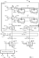
- FIGURE 1 A circuit architecture for selectively boosting a word-line of a cache memory array according to one aspect of the present disclosure is shown in FIGURE 1 .
- FIGURE 1 shows an architecture of a boost scheme for a write word-line according to one aspect of the present disclosure.
- a row boost voltage generator (BVG) 110 (110-1,..., 110-n) is used at the array level to produce a transient boosted voltage on the VDD_BOOST_GL signals 230, as shown in FIGURE 2 .
- a boost timing generator 102 synchronously triggers the BVGs 110 during a write cycle so that the boost is generated immediately following a word-line transition (i.e. a change in word-line voltage).
- the boost timing generator 102 generates a boost_clk signal 112 according to a write enable (Wr_en) signal 104, a clock (clk) signal 106, and a boost enable (boost_en) signal 108.
- the boost timing generator 102 triggers the BVGs 110 according to a timing so that the boost is generated following a word-line transition.
- the BVGs 110 do not have to provide a charge for the initial word-line transitions since the boost_clk signal 112 causes the BVGs 110 to assert the boost voltage following the word-line transition.
- the boosted voltage is hierarchically distributed through power muxes (PM) 120 (120-1, ..., 120-n) down to the local word-line drivers (LWLD) 130 (130-1, ..., 130-n).
- the PM 120 connects the LWLDs 130 on the selected bank 150 (150, ..., 150-n) to a boosted supply voltage VDD_BANK_BOOST signal 126 using a boost voltage VDD_BOOST_GL signal 116, a supply voltage VDD 124, and a bank select signal 122.
- the non-selected bank remains isolated from VDD_BOOST_GL signal 116, thereby reducing a load observed by the BVGs 110.
- bank n-1 may not be selected, and as such, the VDD_BOOST_GL signal 116-n-1 is also not selected so that it does not act as a driver to activate Power Mux 120-n-1.
- the BVGs 110 are distributed along the data I/O (input/output) with one BVG 110 per LWLD column or per byte enable (BE).
- the BE can be write or read and can be used to control byte wide access to external memory, also known as laning.
- the BVGs 110 are tightly controlled by the signals used to access the memory.
- the BE signal 114 and the boost_clk signal 112 enable generation of a transient boost voltage VDD_BOOST_GL signal 116 for a selected byte/word.
- VDD_BOOST_GL signal 116 for a selected byte/word.
- LWLDs 130 of the selected byte/word are boosted. This improves power efficiency, especially on storage unit cache memory arrays such as array 140 made of memory cells (140-1, ..., 140-n).
- the boosted supply voltage VDD_BANK_BOOST signal 126 and the local word line (LWL) 136 are floating, thus during a long write phase, they could leak down to a lower voltage. Due to transistor leakage, the word-line can change its voltage level to a lower voltage (i.e. float) and get into a critical voltage range where the word-line can cause bit-line failures in affected word-line segments.
- the leakage on the boosted supply is managed to guarantee a LWL boost of several nanoseconds at a low voltage to safely complete the write operation.
- the LWLDs 130 (130-1,....,130-n) drive memory cells 140 (140-1, ..., 140-n) in response to a VDD_BANK_BOOST_1 signal 126 (126-1, ..., 126-n), a global word-line (GWL) signal 132 (132-1, ..., 132-n) and a byte enable (BE) signal 134 (134-1, ..., 134-n).
- GWL global word-line
- BE byte enable
- WBLs write bit-lines
- the read word-line boost scheme is similar except that the BVGs 110 directly drives the LWLD 130 without the PM 120 to ensure that boost voltage arrives at the LWL 136 just after the rise of local read word-line.
- the leakage on the boosted supply nodes (such as VDD_BOOST_GL 116 and VDD_BANK_BOOST 126) and the LWL nodes (such as LWL 136) are kept low enough so that the boost voltage remains high for a certain minimum duration. This minimum duration is determined by the minimum time duration which is necessary to complete the read/write operation.
- the leakage is kept low by using lower leakage devices on the boosted supply.
- the boost voltage and LWL are triggered by a common clock signal (such as boost_clk 112) which starts the read/write operation.
- boost_clk 112 which starts the read/write operation.
- the timing of the boost and the LWL is tuned in the design such that boost is triggered just after LWL transition.
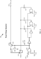
- FIGURE 2 is a circuit diagram further illustrating the voltage boost generator (BVG) 200 (110 of FIGURE 1 ) according to an aspect of the present disclosure.
- the BVG 200 uses gate dielectric coupling capacitors C1-C3 (232, 234 and 236) for generating a boost voltage VDD_BOOST_GL 230.
- the voltage boost generator 200 can be programmed to adjust a boost level in the range of 10%-20% of the supply voltage (VDD) for reads and 25%-35% of the supply voltage (VDD) for writes.
- the BVG 200 initially holds the VDD_BOOST_GL signal 230 at a VDD power supply voltage through P1 (pass transistor 238), and during a write phase, the VDD_BOOST_GL signal 230 is floated (e.g., using float_ctrl signal 248) and then coupled higher through capacitors C1-C3 232-236 through a boost_clk signal 240.
- a level of the boost voltage VDD_BOOST_GL 230 is determined by programming a boost_prog1 signal 242, a boost_prog2 signal 244 and a boost_prog3 signal 246.
- the boost voltage generator (BVG) 200 may contain three (3) programmable pins, such as boost_prog1 signal 242, boost_prog2 signal 244 and boost_prog3 signal 246 which can be controlled to determine how much boost is needed through multiple techniques. Such techniques may be sensor driven or state machine driven to ensure that a successful write is achieved (by controlling the boost). Adjusting the boost level during write and read operations involves manipulation of the supply voltage VDD by performing a Monte Carlo Circuit Analysis. It is known to those skilled in the art that a Monte Carlo circuit analysis is a class of computational algorithms that rely on repeated random sampling to compute the results. They are often used in computer simulations of physical and mathematical systems.
- boost_clk signal 240 to one of the input ports of the NAND gate 202 to timely trigger the voltage manipulation to manage the boost.
- NAND gate 202 is also configured to receive a boost programming signal boost_prog1 signal 242.
- boost_prog1 signal 242 When at least one of the signals boost_clk signal 240 and boost_prog1 signal 242 is a logical LOW, pass transistor 204 is OFF and pull-down transistor 206 is ON which translates into having pass transistor 238 be ON.
- the boost voltage is generated by the boost_clk signal 240.
- Boost_clk signal 240 is triggered only in the cycle when there is read or write operations.
- the generation of boost voltage is tied to the read/write operation on a cycle basis. In many cases the memory operations are infrequent and so less power is dissipated in generating the boost voltage. This is an enhancement over prior art schemes wherein the boost voltage is not controlled on a cycle basis and BVG circuits are left active all the time.
- the word "float" in the BVG operation as a status of a node in operation.
- node goes to a logic value HIGH, such as node 208
- the node VDD_BOOST_GL 230 becomes a floating output, which is subsequently boosted up to a higher voltage through the coupling of the gate dielectric coupling capacitors C1-C3 (232-236).
- the leakage on the boosted supply comes from all the devices connected to it. This includes device 204. This also includes the LWLDs and P5/P6 in FIG. 3 (discussed further below).
- boost_prog1 signal 242 When the programming signal boost_prog1 signal 242 is pulled to a logical HIGH when the boost clock signal boost_clk signal 240 is also at a logic value HIGH, or asserted, pass transistor 204 is ON and pull-down transistor 206 is OFF, which in turn keeps transistor 238 OFF. This isolates the supply voltage Vdd from the output port labeled the voltage signal VDD_BOOST_GL signal 230 and allows it to float. Also, the terminal 232 of capacitor C1 is brought to a logic value HIGH through boost_clk signal 240, which in turn couples the VDD_BOOST_GL signal 230 to a value higher than Vdd.
- boost_prog1 signal 242 and boost_clk signal 240 at a logical HIGH voltage
- boost_prog2 signal 244 is set to a logical HIGH
- the terminal 234 of capacitor C2 is brought to a logic value HIGH through boost_clk signal, which also boosts the voltage at the output port supplying the voltage VDD_BOOST_GL signal 230.
- the signal boost_prog3 signal 246 is set to a logic value HIGH, then the terminal 236 of capacitor C3 is brought to a logic value HIGH, which also boosts the voltage at the output port supplying the voltage VDD_BOOST_GL 230.
- boost_prog2 signal 244 and boost_prog3 signal 246 determine whether the capacitors C2 234 and C3 236 are also boosting the voltage VDD_BOOST_GL signal 230. In this way, adding additional capacitors and associated circuit components with additional programming signals will lead to a higher boost for the supply voltage.
- BVG 200 can be programmed to adjust boost level 10%-20% of the supply voltage (VDD) for reads and 25%-35% of the supply voltage (VDD) for writes these programming signals can be used to adjust how much the supply voltage is boosted.
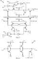
- FIGURE 3 illustrates a power multiplexor (PM) 300 according to one aspect of the present disclosure.
- a multiplexer or MUX is a device that selects one of several analog or digital signals and forwards the selected input inot a single line. Multiplexers are used to increase the amount of data that can be sent over the network within a certain amount of time and bandwidth. Multiplexers can be data selectors as well as power signals. Multiplexers that act as power selectors are called power multiplexers. Typically, a power multiplexer (power MUX) is used to enable seamless transition between two power supplies, or as applied in this case, enables the selection of specific power bank to enable the selection of specific boosted supply.
- the boosted voltage can be hierarchically distributed through power MUX (PM) 300, down to the local WL driver (LWLD), such as LWLD 130 ( FIGURE 1 ).
- the PM 300 connects the LWLD 130 supply to the boosted supply Vdd_boost signal 302 through P3-P4 on the selected bank, whereas in the non-selected bank, the LWDL are connected to VDD through P5-P6.
- Devices P3-P6 can be any type of PFET devices.
- level shifters are used on the signals controlling gates of P3-P6.
- Bank select signal allows for the selection of a bank (1-n) and byte enable signal (BE) allows for the selection to boost in the selected bank (1-n).
- the devices P5 and P6 are off. In order to keep them completely off during the boost phase, it is necessary to keep boost_sel signal 322 to be at the potential of VDD_BOOST_GL signal 324. This is achieved by using level shifters which convert the bank_sel signal 304 in VDD domain to boost_sel signal 322 in the VDD_BOOST_GL signal 324 domain. Without the use of the level shifters, the devices P5 and P6 would not be completely turned off during the boost phase and can cause increased leakage that will eventually dissipate the boosted voltage.
- bank_sel signal 304 is the signal used to select what bank of the cache is used and bank_be_sel signal 306 is a resulting signal of logic AND function of the bank_sel signal 304 and the Byteline Enable (BE) signal 308.
- BE signal 308 is also used to select what byte or group of bits in a particular bank are used.
- PM 300 may implement the use of a number of NAND gates to achieve the appropriate boost voltage that is distributed to the Local Word Line Drivers (LWLD). In one exemplary embodiment illustred in FIG. 3 , PM 300 may incorporate two NAND logic gates 310a and 310b. NAND 310b is primarily used to select whether to boost or not boost the signal.
- NAND 310a is used to determine the output signal.
- the following table better illustrates the value logic system of input and output combinations of PM 300.
- Table 1 Power MUX Input/Output logic BE Bank_Sel Vdd_boost_nor Vdd_boost_inv 0 0 Floating Vdd 0 1 0 Vdd 1 0 Vdd Vdd 1 1 VDD_BOOST_GL VDD_BOOST_GL
- both outputs have a value VDD BOOST GL.
- power mux (PM) 300 reduces the loading on boost voltage generators, such as BVG 200, and thus improves the power efficiency.
- PM 300 is used primarily as a distributor of the boost voltage to LWLD drivers. PM 300 reduces the loading on BVGs and thus improves power efficiency.
- FIGURE 4 illustrates a local word-line driver (LWLD) 400 according to one aspect of the present disclosure.
- the LWLD 400 includes an inverter followed by a NOR2 stage with byte enable gating where both are connected to the boosted supply.
- One series pMOS in the NOR is shared across the column and is merged in the PM 300 to save area.
- Explicit level shifting is avoided in the LWLD 400 for area efficiency.
- VDD_BANK_BOOST signal 126 (shown in FIG. 1 ) represents the boosted output voltage signal from the power mux 120 (shown in greater detail as PM 300).
- the VDD_BANK_BOOST signal 126 translates into two output signals (Vdd_boost_nor signal 312 and Vdd_boos_inv signal 314).
- the global word-line (GWL) signal 432 remains at 0, preventing increased leakage through the LWLDs 400 during a boosted write phase.
- GWL 432 begins to increase in value, rising to a value of Vdd, there is exists a resulting increase in leakage through P2.
- the increased leakage is small as only one row is selected per bank.
- the body of P2 device in LWLD 400 is connected to the regular supply voltage to reduce load on the boosted supply.
- the PM 300 connects the LWLD 400 supply to the boosted supply through P3-P4 on the selected bank, whereas in the non-selected bank, the LWDL 400 are connected to VDD through P5-P6.
- explicit level shifters are used on the signals controlling gates of P3-P6.
- the boosted supply voltage VDD_BANK_BOOST_1 (represented by Vdd_boost_inv signal 314 and Vdd_boost_nor signal 312) and the local word-line (LWL) 436 are floating, thus during a long write phase, they could leak down to a lower voltage. Due to transistor leakage, the word-line can change its voltage level to a lower voltage (i.e. float) and get into a critical voltage range where the word-line can cause bit-line failures in affected word-line segments. The leakage on the boosted supply is managed to guarantee a LWL 436 boost of several nanoseconds at a low voltage to safely complete the write operation.
- the LWLDs 400 drive memory cells (not shown) in response to a VDD_BANK_BOOST_1 signal represented by Vdd_boost_inv signal 314 and Vdd_boost_nor signal 312), a global word-line (GWL) signal 432 and a byte enable signal (BE) (n_bank_be_sel) signal 320.
- the byte enable signal n_bank_be_sel 320 is also the output signal of the NAND 310b device (shown in FIG. 3 ) utilized to select whether to enable boost through the power mux 300 or not.
- the write bit-lines (WBLs) (not shown) are kept driven during the entire write phase, these WBLs are well-known for those who have skill of art.
- the leakage on the boosted supply nodes and the LWL nodes are kept low enough that the boost voltage remains at logic value HIGH for a certain minimum duration. This minimum duration is determined by the minimum time duration which is necessary to complete the read/write operation.
- the leakage is kept low by using lower leakage devices on the boosted supply.
- the boost and LWL are triggered by a common clock signal which starts the read/write operation. The timing of the boost and LWL is turned in the design such that boost is triggered just after LWL transition.
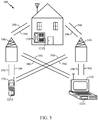
- FIGURE 5 shows an exemplary wireless communication system 500 in which an embodiment of the disclosure may be advantageously employed.
- FIGURE 5 shows three remote units 520, 530, and 550 and two base stations 540. It will be recognized that typical wireless communication systems may have many more remote units and base stations.
- Remote units 520, 530, and 550 include adaptive write word line boosting circuitry 525A, 525B, and 525C, respectively, which are embodiments of the disclosure as discussed further below.
- FIGURE 5 shows forward link signals 580 from the base stations 540 and the remote units 520, 530, and 550 and reverse link signals 590 from the remote units 520, 530, and 550 to base stations 540.
- remote unit 520 is shown as a mobile telephone
- remote unit 530 is shown as a portable computer
- remote unit 550 is shown as a fixed location remote unit in a wireless local loop system.
- the remote units may be cell phones, hand-held personal communication systems (PCS) units, portable data units such as personal data assistants, or fixed location data units such as meter reading equipment.
- PCS personal communication systems
- FIGURE 5 illustrates remote units according to the teachings of the disclosure, the disclosure is not limited to these exemplary illustrated units. The disclosure may be suitably employed in any device which includes adaptive write word line boosting circuitry.
- FIG. 6 illustrates cellular phone network 602 comprising Base Stations 604A, 604B, and 604C.
- Figure 6 shows a communication device, labeled 606, which may be a mobile cellular communication device such as a so-called smart phone, a tablet, or some other kind of communication device suitable for a cellular phone network.
- Communication Device 606 need not be mobile.
- Communication Device 606 is located within the cell associated with Base Station 604C.
- Arrows 608 and 610 pictorially represent the uplink channel and the downlink channel, respectively, by which Communication Device 606 communicates with Base Station 604C.
- Embodiments may be used in data processing systems associated with Communication Device 606, or with Base Station 604C, or both, for example.
- Figure 6 illustrates only one application among many in which the embodiments described herein may be employed.
- FIGURE 7 illustrates one exemplary method for selective word-line boost on a memory cell, wherein the method comprises receiving a clock signal to trigger boost timing operations 702.
- the boost timing operations are initiated in a boost timing generator and a boost clock signal is forwarded to a boost voltage generator.
- the voltage generator then generates a selected transient boost voltage 704 to be locally delivered and enabled during selected cycles of operation.
- the system 700 may then provide a trigger signal to bank array to trigger a bank selection for which a boost voltage signal is to be received 706.
- the transient boost voltage may then be distributed to local word-line drivers on a selected bank array 708.
Landscapes
- Engineering & Computer Science (AREA)
- Microelectronics & Electronic Packaging (AREA)
- Computer Hardware Design (AREA)
- Static Random-Access Memory (AREA)
Claims (12)
- Une matrice de mémoires vives statiques, SRAM, à ports multiples, comprenant :un circuit logique de commande comprenant une pluralité de circuits de génération de tension (110, 200) et une pluralité de multiplexeurs de puissance (120, 300), chaque circuit de génération de tension étant configuré de façon à recevoir un signal d'horloge d'amplification (112, 240) et à générer une pluralité de tensions d'amplification transitoires (116, 230), etune pluralité de pilotes de ligne de mots locaux (130) destinés à l'application de la tension d'amplification transitoire de façon à accroître une partie sélectionnée d'une tension de ligne de mots suite à une transition de ligne de mots, où la tension d'amplification transitoire est appliquée au pilote de ligne de mots local (130) et la génération de la tension d'amplification transitoire est régulée en fonction d'un cycle de lecture ou d'écriture, et oùle circuit logique de commande comprend un circuit de génération de tension (110, 200) pour chaque colonne de pilotes de ligne de mots locaux de la matrice de mémoires SRAM à ports multiples, le circuit de génération de tension (110, 200) étant configuré de façon à activer une tension d'amplification transitoire suite à une transition de ligne de mots.
- La matrice de mémoires SRAM à ports multiples selon la Revendication 1, dans laquelle le circuit logique de commande comprend un circuit de génération de tension pour chaque pilote de ligne de mots local (130) à l'intérieur de chaque colonne de pilotes de ligne de mots locaux de la matrice de mémoires SRAM à ports multiples, le circuit de génération de tension étant configuré de façon à activer un tension d'amplification transitoire suite à une transition de ligne de mots.
- La matrice de mémoires SRAM à ports multiples selon la Revendication 2, dans laquelle le circuit de génération de tension (110, 200) comprend :une pluralité de condensateurs de couplage diélectriques à grille (232, 234, 236),une section de charge raccordant la pluralité de condensateurs de couplage diélectriques à grille en série, où la section de charge est configurée de façon à recevoir au moins un signal de commande d'amplification (242, 244, 246)et où la section de charge est configurée de façon à ajuster un niveau d'amplification à l'intérieur d'une plage spécifiée pour des opérations de lecture et d'écriture.
- La matrice de mémoires SRAM à ports multiples selon la Revendication 1, où le circuit de génération de tension comprend un circuit d'amplification configuré de façon à générer la tension d'amplification transitoire au niveau d'une colonne de pilotes de ligne de mots locaux et configuré en outre de façon à distribuer la tension d'amplification transitoire aux pilotes de ligne de mots locaux (130).
- La matrice de mémoires SRAM à ports multiples selon la Revendication 4, où :le multiplexeur de puissance (120, 300) est configuré de façon à produire en sortie au moins deux tensions en sortie à distribuer vers les pilotes de ligne de mots locaux (130), oula génération d'une amplification de tension transitoire est désactivée lorsqu'une matrice de blocs n'est pas accédée.
- La matrice de mémoires SRAM à ports multiples selon la Revendication 4, où le multiplexeur de puissance comprend en outre un premier circuit de multiplexage configuré de façon à sélectionner une matrice de blocs à activer pour une génération d'amplification, et un deuxième circuit de multiplexage configuré de façon à déterminer s'il convient ou non de générer la tension d'amplification transitoire, et où le deuxième circuit de multiplexage est raccordé de manière opérationnelle au premier circuit de multiplexage, et où l'entrée du premier circuit de multiplexage comprend un signal de sélection de bloc (304) et un signal d'activation d'octet inversé (308).
- Un procédé d'amplification de ligne de mots sélective sur une matrice de mémoires SRAM à ports multiples selon la Revendication 1 comprenant :la réception d'un signal d'horloge (112) destiné au déclenchement d'opérations de synchronisation d'amplification,la génération d'une tension d'amplification transitoire sélectionnée (116, 230),la commande de la génération de la tension d'amplification transitoire en fonction d'un cycle de lecture ou d'écriture,la fourniture d'un signal de déclenchement (152) à une matrice de blocs (140) destiné au déclenchement d'une sélection de matrice de blocs,la distribution de la tension d'amplification transitoire sélectionnée à la matrice de blocs sélectionnée,la réception de la tension d'amplification transitoire (116, 230) au niveau d'un multiplexeur de puissance (120, 300),l'application de la tension d'amplification transitoire de façon à accroître une partie sélectionnée d'une tension de ligne de mots fournie par un pilote de tension de ligne de mots local (130), suite à une transition de ligne de mots, etl'activation de la tension d'amplification transitoire, suite à une transition de ligne de mots, pour chaque colonne de pilotes de ligne de mots locaux de la matrice de mémoires SRAM à ports multiples.
- Le procédé selon la Revendication 7, comprenant en outre la configuration d'un circuit de génération de tension de façon à activer la tension d'amplification transitoire pour chaque pilote de tension de ligne de mots local (130) à l'intérieur de chaque colonne de pilotes de ligne de mots locaux de la matrice de mémoires SRAM à ports multiples.
- Le procédé selon la Revendication 8, où la configuration du circuit de génération de tension comprend en outre :le couplage d'une pluralité de condensateurs diélectriques à grille (232, 234, 236) en série, etla fourniture d'une section de charge configurée de façon à recevoir au moins un signal de commande d'amplification (242, 244, 246) et configurée en outre de façon à ajuster un niveau d'amplification à l'intérieur d'une plage spécifiée pour des opérations de lecture et d'écriture.
- Le procédé selon la Revendication 7, comprenant en outre la configuration d'un circuit d'amplification de façon à générer la tension d'amplification transitoire au niveau d'une colonne de pilotes de ligne de mots locaux et en outre la configuration du circuit d'amplification de façon à distribuer la tension d'amplification transitoire vers les pilotes de tension de ligne de mots locaux (130).
- Le procédé selon la Revendication 7, comprenant en outre l'application de la tension d'amplification transitoire sélectionnée au niveau d'un pilote de ligne de mots local (130).
- Le procédé selon la Revendication 11, comprenant en outre :la génération d'au moins deux tensions en sortie (312, 314) configurées de façon à être distribuées vers les pilotes de ligne de mots locaux (130), oula désactivation de la génération de l'amplification de tension transitoire lorsqu'une matrice de blocs n'est pas accédée.
Applications Claiming Priority (4)
| Application Number | Priority Date | Filing Date | Title |
|---|---|---|---|
| US201161533730P | 2011-09-12 | 2011-09-12 | |
| US201161533745P | 2011-09-12 | 2011-09-12 | |
| US13/609,520 US8724373B2 (en) | 2011-09-12 | 2012-09-11 | Apparatus for selective word-line boost on a memory cell |
| PCT/US2012/054902 WO2013040061A1 (fr) | 2011-09-12 | 2012-09-12 | Appareil permettant une amplification sélective de la tension de ligne de mots sur une cellule de mémoire |
Publications (2)
| Publication Number | Publication Date |
|---|---|
| EP2756500A1 EP2756500A1 (fr) | 2014-07-23 |
| EP2756500B1 true EP2756500B1 (fr) | 2020-04-15 |
Family
ID=47829737
Family Applications (1)
| Application Number | Title | Priority Date | Filing Date |
|---|---|---|---|
| EP12769230.9A Active EP2756500B1 (fr) | 2011-09-12 | 2012-09-12 | Appareil permettant une amplification sélective de la tension de ligne de mots sur une cellule de mémoire |
Country Status (6)
| Country | Link |
|---|---|
| US (1) | US8724373B2 (fr) |
| EP (1) | EP2756500B1 (fr) |
| JP (1) | JP6030653B2 (fr) |
| KR (1) | KR101678034B1 (fr) |
| CN (2) | CN111145805A (fr) |
| WO (1) | WO2013040061A1 (fr) |
Families Citing this family (21)
| Publication number | Priority date | Publication date | Assignee | Title |
|---|---|---|---|---|
| US8659972B2 (en) * | 2011-09-12 | 2014-02-25 | Qualcomm Incorporated | Adaptive read wordline voltage boosting apparatus and method for multi-port SRAM |
| US9142275B2 (en) * | 2012-10-31 | 2015-09-22 | Taiwan Semiconductor Manufacturing Co., Ltd. | Wordline tracking for boosted-wordline timing scheme |
| US9030863B2 (en) | 2013-09-26 | 2015-05-12 | Qualcomm Incorporated | Read/write assist for memories |
| US9502119B2 (en) * | 2014-11-20 | 2016-11-22 | Samsung Electronics Co., Ltd. | Distributed capacitive delay tracking boost-assist circuit |
| CN104464797B (zh) * | 2014-12-23 | 2017-12-12 | 苏州宽温电子科技有限公司 | 一种自适应的字线电压调节型sram结构 |
| US10026456B2 (en) * | 2015-02-23 | 2018-07-17 | Qualcomm Incorporated | Bitline positive boost write-assist circuits for memory bit cells employing a P-type Field-Effect transistor (PFET) write port(s), and related systems and methods |
| CN105070316B (zh) * | 2015-08-27 | 2018-02-06 | 安徽大学 | 一种具有复制单元字线电压抬升技术的sram时序控制电路 |
| KR102374228B1 (ko) | 2015-08-27 | 2022-03-15 | 삼성전자주식회사 | 저항성 메모리 장치의 부스트 전압 생성기, 이를 포함하는 전압 생성기 및 이를 포함하는 저항성 메모리 장치 |
| US9620509B1 (en) * | 2015-10-30 | 2017-04-11 | Taiwan Semiconductor Manufacturing Co., Ltd. | Static random access memory device with vertical FET devices |
| US10163524B2 (en) | 2016-06-22 | 2018-12-25 | Darryl G. Walker | Testing a semiconductor device including a voltage detection circuit and temperature detection circuit that can be used to generate read assist and/or write assist in an SRAM circuit portion and method therefor |
| US9940999B2 (en) | 2016-06-22 | 2018-04-10 | Darryl G. Walker | Semiconductor devices, circuits and methods for read and/or write assist of an SRAM circuit portion based on voltage detection and/or temperature detection circuits |
| US10171080B2 (en) * | 2016-09-20 | 2019-01-01 | Qualcomm Incorporated | Voltage level shifter (VLS) circuits employing a pre-conditioning circuit for pre-conditioning an input signal to be voltage level shifted in response to a pre-charge phase |
| US9633706B1 (en) | 2016-10-10 | 2017-04-25 | Qualcomm Incorporated | Voltage self-boosting circuit for generating a boosted voltage for driving a word line write in a memory array for a memory write operation |
| US10553275B2 (en) * | 2017-04-18 | 2020-02-04 | Taiwan Semiconductor Manufacturing Company, Ltd. | Device having write assist circuit including memory-adapted transistors and method for making the same |
| KR102360213B1 (ko) | 2017-09-06 | 2022-02-08 | 삼성전자주식회사 | 칩 사이즈를 감소한 저항성 메모리 장치 및 그 동작방법 |
| US10692567B2 (en) | 2018-09-06 | 2020-06-23 | M31 Technology Corporation | Method for assisting memory cell in access operation and operating memory cell, and memory device having assist circuit with predefined assist strength |
| US11069415B2 (en) | 2018-10-05 | 2021-07-20 | Samsung Electronics Co., Ltd. | Memory device including charge pump circuit |
| KR102545174B1 (ko) * | 2018-10-05 | 2023-06-19 | 삼성전자주식회사 | 차지 펌프 회로를 포함하는 메모리 장치 |
| KR102830171B1 (ko) | 2020-02-25 | 2025-07-07 | 삼성전자주식회사 | 불휘발성 메모리 장치 및 불휘발성 메모리 장치의 동작 방법 |
| US11955171B2 (en) | 2021-09-15 | 2024-04-09 | Mavagail Technology, LLC | Integrated circuit device including an SRAM portion having end power select circuits |
| US12525976B2 (en) * | 2023-06-05 | 2026-01-13 | Advanced Energy Industries, Inc. | Active switch leakage current diversion |
Family Cites Families (11)
| Publication number | Priority date | Publication date | Assignee | Title |
|---|---|---|---|---|
| JPH05120881A (ja) | 1991-10-24 | 1993-05-18 | Mitsubishi Electric Corp | 半導体記憶装置 |
| JPH0945082A (ja) | 1995-07-26 | 1997-02-14 | Nec Corp | 半導体メモリ |
| JPH10228773A (ja) * | 1997-02-14 | 1998-08-25 | Hitachi Ltd | ダイナミック型ram |
| JP2000003598A (ja) | 1998-06-15 | 2000-01-07 | Nec Corp | ブースト回路及びこれを備える半導体記憶装置 |
| JP2003281893A (ja) * | 2002-03-22 | 2003-10-03 | Seiko Epson Corp | 半導体記憶装置及び電子機器 |
| KR20040006384A (ko) * | 2002-07-12 | 2004-01-24 | 주식회사 하이닉스반도체 | 오버드라이빙 제어 장치 |
| JP4439185B2 (ja) * | 2003-02-07 | 2010-03-24 | パナソニック株式会社 | 半導体記憶装置 |
| US6798275B1 (en) | 2003-04-03 | 2004-09-28 | Advanced Micro Devices, Inc. | Fast, accurate and low power supply voltage booster using A/D converter |
| US7636254B2 (en) | 2006-09-18 | 2009-12-22 | International Business Machines Corporation | Wordline booster circuit and method of operating a wordline booster circuit |
| US7961499B2 (en) * | 2009-01-22 | 2011-06-14 | Qualcomm Incorporated | Low leakage high performance static random access memory cell using dual-technology transistors |
| US8300451B2 (en) | 2010-03-30 | 2012-10-30 | Texas Instruments Incorporated | Two word line SRAM cell with strong-side word line boost for write provided by weak-side word line |
-
2012
- 2012-09-11 US US13/609,520 patent/US8724373B2/en not_active Expired - Fee Related
- 2012-09-12 WO PCT/US2012/054902 patent/WO2013040061A1/fr not_active Ceased
- 2012-09-12 JP JP2014529986A patent/JP6030653B2/ja not_active Expired - Fee Related
- 2012-09-12 KR KR1020147009846A patent/KR101678034B1/ko not_active Expired - Fee Related
- 2012-09-12 CN CN201911303858.4A patent/CN111145805A/zh active Pending
- 2012-09-12 CN CN201280043879.7A patent/CN103797538A/zh active Pending
- 2012-09-12 EP EP12769230.9A patent/EP2756500B1/fr active Active
Non-Patent Citations (1)
| Title |
|---|
| None * |
Also Published As
| Publication number | Publication date |
|---|---|
| KR101678034B1 (ko) | 2016-11-21 |
| US20130064006A1 (en) | 2013-03-14 |
| CN111145805A (zh) | 2020-05-12 |
| KR20140063813A (ko) | 2014-05-27 |
| US8724373B2 (en) | 2014-05-13 |
| EP2756500A1 (fr) | 2014-07-23 |
| JP6030653B2 (ja) | 2016-11-24 |
| JP2014526765A (ja) | 2014-10-06 |
| CN103797538A (zh) | 2014-05-14 |
| WO2013040061A1 (fr) | 2013-03-21 |
Similar Documents
| Publication | Publication Date | Title |
|---|---|---|
| EP2756500B1 (fr) | Appareil permettant une amplification sélective de la tension de ligne de mots sur une cellule de mémoire | |
| US10032507B2 (en) | SRAM bit-line and write assist apparatus and method for lowering dynamic power and peak current, and a dual input level-shifter | |
| KR100964266B1 (ko) | 저전력 고성능의 메모리셀 및 관련방법 | |
| US7705625B2 (en) | Source transistor configurations and control methods | |
| JP5822914B2 (ja) | 高性能スタティックメモリのリテイン・ティル・アクセスド(rta)省電力モード | |
| US7327630B2 (en) | Memory cell power switching circuit in semiconductor memory device and method for applying memory cell power voltage | |
| KR101522376B1 (ko) | 복수의 정적 랜덤-액세스 메모리 셀들을 포함하는 디바이스 및 그 동작 방법 | |
| US20140233330A1 (en) | Write assist circuit, memory device and method | |
| US20080151653A1 (en) | Semiconductor memory device | |
| US8462541B2 (en) | Circuits and methods for reducing minimum supply for register file cells | |
| US20100039872A1 (en) | Dual Power Scheme in Memory Circuit | |
| US8379465B2 (en) | Combined write assist and retain-till-accessed memory array bias | |
| US20040105299A1 (en) | Storage array such as a SRAM with reduced power requirements | |
| KR20050123400A (ko) | 메모리 장치의 파워 노이즈를 방지하는 직렬 웨이크 업 회로 | |
| US9542996B2 (en) | Device with SRAM memory cells including means for polarizing wells of memory cell transistors | |
| KR20220056785A (ko) | 멀티 뱅크 sram에서 전력 관리 모드를 위한 비트 라인 프리차지 회로 | |
| US10878853B2 (en) | Power supply control | |
| US6396336B2 (en) | Sleep mode VDD detune for power reduction |
Legal Events
| Date | Code | Title | Description |
|---|---|---|---|
| PUAI | Public reference made under article 153(3) epc to a published international application that has entered the european phase |
Free format text: ORIGINAL CODE: 0009012 |
|
| 17P | Request for examination filed |
Effective date: 20140213 |
|
| AK | Designated contracting states |
Kind code of ref document: A1 Designated state(s): AL AT BE BG CH CY CZ DE DK EE ES FI FR GB GR HR HU IE IS IT LI LT LU LV MC MK MT NL NO PL PT RO RS SE SI SK SM TR |
|
| DAX | Request for extension of the european patent (deleted) | ||
| STAA | Information on the status of an ep patent application or granted ep patent |
Free format text: STATUS: EXAMINATION IS IN PROGRESS |
|
| 17Q | First examination report despatched |
Effective date: 20190405 |
|
| GRAP | Despatch of communication of intention to grant a patent |
Free format text: ORIGINAL CODE: EPIDOSNIGR1 |
|
| STAA | Information on the status of an ep patent application or granted ep patent |
Free format text: STATUS: GRANT OF PATENT IS INTENDED |
|
| INTG | Intention to grant announced |
Effective date: 20191031 |
|
| GRAS | Grant fee paid |
Free format text: ORIGINAL CODE: EPIDOSNIGR3 |
|
| GRAA | (expected) grant |
Free format text: ORIGINAL CODE: 0009210 |
|
| STAA | Information on the status of an ep patent application or granted ep patent |
Free format text: STATUS: THE PATENT HAS BEEN GRANTED |
|
| AK | Designated contracting states |
Kind code of ref document: B1 Designated state(s): AL AT BE BG CH CY CZ DE DK EE ES FI FR GB GR HR HU IE IS IT LI LT LU LV MC MK MT NL NO PL PT RO RS SE SI SK SM TR |
|
| REG | Reference to a national code |
Ref country code: CH Ref legal event code: EP Ref country code: GB Ref legal event code: FG4D |
|
| REG | Reference to a national code |
Ref country code: DE Ref legal event code: R096 Ref document number: 602012069305 Country of ref document: DE |
|
| REG | Reference to a national code |
Ref country code: IE Ref legal event code: FG4D |
|
| REG | Reference to a national code |
Ref country code: AT Ref legal event code: REF Ref document number: 1258221 Country of ref document: AT Kind code of ref document: T Effective date: 20200515 |
|
| REG | Reference to a national code |
Ref country code: NL Ref legal event code: MP Effective date: 20200415 |
|
| REG | Reference to a national code |
Ref country code: LT Ref legal event code: MG4D |
|
| PG25 | Lapsed in a contracting state [announced via postgrant information from national office to epo] |
Ref country code: NO Free format text: LAPSE BECAUSE OF FAILURE TO SUBMIT A TRANSLATION OF THE DESCRIPTION OR TO PAY THE FEE WITHIN THE PRESCRIBED TIME-LIMIT Effective date: 20200715 Ref country code: FI Free format text: LAPSE BECAUSE OF FAILURE TO SUBMIT A TRANSLATION OF THE DESCRIPTION OR TO PAY THE FEE WITHIN THE PRESCRIBED TIME-LIMIT Effective date: 20200415 Ref country code: GR Free format text: LAPSE BECAUSE OF FAILURE TO SUBMIT A TRANSLATION OF THE DESCRIPTION OR TO PAY THE FEE WITHIN THE PRESCRIBED TIME-LIMIT Effective date: 20200716 Ref country code: SE Free format text: LAPSE BECAUSE OF FAILURE TO SUBMIT A TRANSLATION OF THE DESCRIPTION OR TO PAY THE FEE WITHIN THE PRESCRIBED TIME-LIMIT Effective date: 20200415 Ref country code: IS Free format text: LAPSE BECAUSE OF FAILURE TO SUBMIT A TRANSLATION OF THE DESCRIPTION OR TO PAY THE FEE WITHIN THE PRESCRIBED TIME-LIMIT Effective date: 20200815 Ref country code: NL Free format text: LAPSE BECAUSE OF FAILURE TO SUBMIT A TRANSLATION OF THE DESCRIPTION OR TO PAY THE FEE WITHIN THE PRESCRIBED TIME-LIMIT Effective date: 20200415 Ref country code: LT Free format text: LAPSE BECAUSE OF FAILURE TO SUBMIT A TRANSLATION OF THE DESCRIPTION OR TO PAY THE FEE WITHIN THE PRESCRIBED TIME-LIMIT Effective date: 20200415 Ref country code: PT Free format text: LAPSE BECAUSE OF FAILURE TO SUBMIT A TRANSLATION OF THE DESCRIPTION OR TO PAY THE FEE WITHIN THE PRESCRIBED TIME-LIMIT Effective date: 20200817 |
|
| REG | Reference to a national code |
Ref country code: AT Ref legal event code: MK05 Ref document number: 1258221 Country of ref document: AT Kind code of ref document: T Effective date: 20200415 |
|
| PG25 | Lapsed in a contracting state [announced via postgrant information from national office to epo] |
Ref country code: BG Free format text: LAPSE BECAUSE OF FAILURE TO SUBMIT A TRANSLATION OF THE DESCRIPTION OR TO PAY THE FEE WITHIN THE PRESCRIBED TIME-LIMIT Effective date: 20200715 Ref country code: LV Free format text: LAPSE BECAUSE OF FAILURE TO SUBMIT A TRANSLATION OF THE DESCRIPTION OR TO PAY THE FEE WITHIN THE PRESCRIBED TIME-LIMIT Effective date: 20200415 Ref country code: RS Free format text: LAPSE BECAUSE OF FAILURE TO SUBMIT A TRANSLATION OF THE DESCRIPTION OR TO PAY THE FEE WITHIN THE PRESCRIBED TIME-LIMIT Effective date: 20200415 Ref country code: HR Free format text: LAPSE BECAUSE OF FAILURE TO SUBMIT A TRANSLATION OF THE DESCRIPTION OR TO PAY THE FEE WITHIN THE PRESCRIBED TIME-LIMIT Effective date: 20200415 |
|
| PG25 | Lapsed in a contracting state [announced via postgrant information from national office to epo] |
Ref country code: AL Free format text: LAPSE BECAUSE OF FAILURE TO SUBMIT A TRANSLATION OF THE DESCRIPTION OR TO PAY THE FEE WITHIN THE PRESCRIBED TIME-LIMIT Effective date: 20200415 |
|
| REG | Reference to a national code |
Ref country code: DE Ref legal event code: R097 Ref document number: 602012069305 Country of ref document: DE |
|
| PG25 | Lapsed in a contracting state [announced via postgrant information from national office to epo] |
Ref country code: DK Free format text: LAPSE BECAUSE OF FAILURE TO SUBMIT A TRANSLATION OF THE DESCRIPTION OR TO PAY THE FEE WITHIN THE PRESCRIBED TIME-LIMIT Effective date: 20200415 Ref country code: SM Free format text: LAPSE BECAUSE OF FAILURE TO SUBMIT A TRANSLATION OF THE DESCRIPTION OR TO PAY THE FEE WITHIN THE PRESCRIBED TIME-LIMIT Effective date: 20200415 Ref country code: EE Free format text: LAPSE BECAUSE OF FAILURE TO SUBMIT A TRANSLATION OF THE DESCRIPTION OR TO PAY THE FEE WITHIN THE PRESCRIBED TIME-LIMIT Effective date: 20200415 Ref country code: AT Free format text: LAPSE BECAUSE OF FAILURE TO SUBMIT A TRANSLATION OF THE DESCRIPTION OR TO PAY THE FEE WITHIN THE PRESCRIBED TIME-LIMIT Effective date: 20200415 Ref country code: CZ Free format text: LAPSE BECAUSE OF FAILURE TO SUBMIT A TRANSLATION OF THE DESCRIPTION OR TO PAY THE FEE WITHIN THE PRESCRIBED TIME-LIMIT Effective date: 20200415 Ref country code: IT Free format text: LAPSE BECAUSE OF FAILURE TO SUBMIT A TRANSLATION OF THE DESCRIPTION OR TO PAY THE FEE WITHIN THE PRESCRIBED TIME-LIMIT Effective date: 20200415 Ref country code: ES Free format text: LAPSE BECAUSE OF FAILURE TO SUBMIT A TRANSLATION OF THE DESCRIPTION OR TO PAY THE FEE WITHIN THE PRESCRIBED TIME-LIMIT Effective date: 20200415 Ref country code: RO Free format text: LAPSE BECAUSE OF FAILURE TO SUBMIT A TRANSLATION OF THE DESCRIPTION OR TO PAY THE FEE WITHIN THE PRESCRIBED TIME-LIMIT Effective date: 20200415 |
|
| PLBE | No opposition filed within time limit |
Free format text: ORIGINAL CODE: 0009261 |
|
| STAA | Information on the status of an ep patent application or granted ep patent |
Free format text: STATUS: NO OPPOSITION FILED WITHIN TIME LIMIT |
|
| PG25 | Lapsed in a contracting state [announced via postgrant information from national office to epo] |
Ref country code: PL Free format text: LAPSE BECAUSE OF FAILURE TO SUBMIT A TRANSLATION OF THE DESCRIPTION OR TO PAY THE FEE WITHIN THE PRESCRIBED TIME-LIMIT Effective date: 20200415 Ref country code: SK Free format text: LAPSE BECAUSE OF FAILURE TO SUBMIT A TRANSLATION OF THE DESCRIPTION OR TO PAY THE FEE WITHIN THE PRESCRIBED TIME-LIMIT Effective date: 20200415 |
|
| 26N | No opposition filed |
Effective date: 20210118 |
|
| PG25 | Lapsed in a contracting state [announced via postgrant information from national office to epo] |
Ref country code: MC Free format text: LAPSE BECAUSE OF FAILURE TO SUBMIT A TRANSLATION OF THE DESCRIPTION OR TO PAY THE FEE WITHIN THE PRESCRIBED TIME-LIMIT Effective date: 20200415 |
|
| REG | Reference to a national code |
Ref country code: CH Ref legal event code: PL |
|
| PG25 | Lapsed in a contracting state [announced via postgrant information from national office to epo] |
Ref country code: SI Free format text: LAPSE BECAUSE OF FAILURE TO SUBMIT A TRANSLATION OF THE DESCRIPTION OR TO PAY THE FEE WITHIN THE PRESCRIBED TIME-LIMIT Effective date: 20200415 |
|
| REG | Reference to a national code |
Ref country code: BE Ref legal event code: MM Effective date: 20200930 |
|
| PG25 | Lapsed in a contracting state [announced via postgrant information from national office to epo] |
Ref country code: LU Free format text: LAPSE BECAUSE OF NON-PAYMENT OF DUE FEES Effective date: 20200912 |
|
| PG25 | Lapsed in a contracting state [announced via postgrant information from national office to epo] |
Ref country code: IE Free format text: LAPSE BECAUSE OF NON-PAYMENT OF DUE FEES Effective date: 20200912 Ref country code: LI Free format text: LAPSE BECAUSE OF NON-PAYMENT OF DUE FEES Effective date: 20200930 Ref country code: BE Free format text: LAPSE BECAUSE OF NON-PAYMENT OF DUE FEES Effective date: 20200930 Ref country code: CH Free format text: LAPSE BECAUSE OF NON-PAYMENT OF DUE FEES Effective date: 20200930 |
|
| PG25 | Lapsed in a contracting state [announced via postgrant information from national office to epo] |
Ref country code: TR Free format text: LAPSE BECAUSE OF FAILURE TO SUBMIT A TRANSLATION OF THE DESCRIPTION OR TO PAY THE FEE WITHIN THE PRESCRIBED TIME-LIMIT Effective date: 20200415 Ref country code: MT Free format text: LAPSE BECAUSE OF FAILURE TO SUBMIT A TRANSLATION OF THE DESCRIPTION OR TO PAY THE FEE WITHIN THE PRESCRIBED TIME-LIMIT Effective date: 20200415 Ref country code: CY Free format text: LAPSE BECAUSE OF FAILURE TO SUBMIT A TRANSLATION OF THE DESCRIPTION OR TO PAY THE FEE WITHIN THE PRESCRIBED TIME-LIMIT Effective date: 20200415 |
|
| PG25 | Lapsed in a contracting state [announced via postgrant information from national office to epo] |
Ref country code: MK Free format text: LAPSE BECAUSE OF FAILURE TO SUBMIT A TRANSLATION OF THE DESCRIPTION OR TO PAY THE FEE WITHIN THE PRESCRIBED TIME-LIMIT Effective date: 20200415 |
|
| PGFP | Annual fee paid to national office [announced via postgrant information from national office to epo] |
Ref country code: DE Payment date: 20250808 Year of fee payment: 14 |
|
| PGFP | Annual fee paid to national office [announced via postgrant information from national office to epo] |
Ref country code: GB Payment date: 20250814 Year of fee payment: 14 |
|
| PGFP | Annual fee paid to national office [announced via postgrant information from national office to epo] |
Ref country code: FR Payment date: 20250808 Year of fee payment: 14 |