EP2827490B1 - Système et procédé d'injection de tension de mode commun - Google Patents
Système et procédé d'injection de tension de mode commun Download PDFInfo
- Publication number
- EP2827490B1 EP2827490B1 EP14175253.5A EP14175253A EP2827490B1 EP 2827490 B1 EP2827490 B1 EP 2827490B1 EP 14175253 A EP14175253 A EP 14175253A EP 2827490 B1 EP2827490 B1 EP 2827490B1
- Authority
- EP
- European Patent Office
- Prior art keywords
- current
- minimum
- cmv
- maximum
- signal
- Prior art date
- Legal status (The legal status is an assumption and is not a legal conclusion. Google has not performed a legal analysis and makes no representation as to the accuracy of the status listed.)
- Active
Links
Images


Classifications
-
- H—ELECTRICITY
- H02—GENERATION; CONVERSION OR DISTRIBUTION OF ELECTRIC POWER
- H02M—APPARATUS FOR CONVERSION BETWEEN AC AND AC, BETWEEN AC AND DC, OR BETWEEN DC AND DC, AND FOR USE WITH MAINS OR SIMILAR POWER SUPPLY SYSTEMS; CONVERSION OF DC OR AC INPUT POWER INTO SURGE OUTPUT POWER; CONTROL OR REGULATION THEREOF
- H02M7/00—Conversion of AC power input into DC power output; Conversion of DC power input into AC power output
- H02M7/42—Conversion of DC power input into AC power output without possibility of reversal
- H02M7/44—Conversion of DC power input into AC power output without possibility of reversal by static converters
- H02M7/48—Conversion of DC power input into AC power output without possibility of reversal by static converters using discharge tubes with control electrode or semiconductor devices with control electrode
- H02M7/483—Converters with outputs that each can have more than two voltages levels
- H02M7/487—Neutral point clamped inverters
-
- H—ELECTRICITY
- H02—GENERATION; CONVERSION OR DISTRIBUTION OF ELECTRIC POWER
- H02M—APPARATUS FOR CONVERSION BETWEEN AC AND AC, BETWEEN AC AND DC, OR BETWEEN DC AND DC, AND FOR USE WITH MAINS OR SIMILAR POWER SUPPLY SYSTEMS; CONVERSION OF DC OR AC INPUT POWER INTO SURGE OUTPUT POWER; CONTROL OR REGULATION THEREOF
- H02M5/00—Conversion of AC power input into AC power output, e.g. for change of voltage, for change of frequency, for change of number of phases
- H02M5/40—Conversion of AC power input into AC power output, e.g. for change of voltage, for change of frequency, for change of number of phases with intermediate conversion into DC
- H02M5/42—Conversion of AC power input into AC power output, e.g. for change of voltage, for change of frequency, for change of number of phases with intermediate conversion into DC by static converters
- H02M5/44—Conversion of AC power input into AC power output, e.g. for change of voltage, for change of frequency, for change of number of phases with intermediate conversion into DC by static converters using discharge tubes or semiconductor devices to convert the intermediate DC into AC
- H02M5/453—Conversion of AC power input into AC power output, e.g. for change of voltage, for change of frequency, for change of number of phases with intermediate conversion into DC by static converters using discharge tubes or semiconductor devices to convert the intermediate DC into AC using devices of a triode or transistor type requiring continuous application of a control signal
- H02M5/458—Conversion of AC power input into AC power output, e.g. for change of voltage, for change of frequency, for change of number of phases with intermediate conversion into DC by static converters using discharge tubes or semiconductor devices to convert the intermediate DC into AC using devices of a triode or transistor type requiring continuous application of a control signal using semiconductor devices only
- H02M5/4585—Conversion of AC power input into AC power output, e.g. for change of voltage, for change of frequency, for change of number of phases with intermediate conversion into DC by static converters using discharge tubes or semiconductor devices to convert the intermediate DC into AC using devices of a triode or transistor type requiring continuous application of a control signal using semiconductor devices only having a rectifier with controlled elements
-
- H—ELECTRICITY
- H02—GENERATION; CONVERSION OR DISTRIBUTION OF ELECTRIC POWER
- H02M—APPARATUS FOR CONVERSION BETWEEN AC AND AC, BETWEEN AC AND DC, OR BETWEEN DC AND DC, AND FOR USE WITH MAINS OR SIMILAR POWER SUPPLY SYSTEMS; CONVERSION OF DC OR AC INPUT POWER INTO SURGE OUTPUT POWER; CONTROL OR REGULATION THEREOF
- H02M7/00—Conversion of AC power input into DC power output; Conversion of DC power input into AC power output
- H02M7/42—Conversion of DC power input into AC power output without possibility of reversal
- H02M7/44—Conversion of DC power input into AC power output without possibility of reversal by static converters
- H02M7/48—Conversion of DC power input into AC power output without possibility of reversal by static converters using discharge tubes with control electrode or semiconductor devices with control electrode
- H02M7/483—Converters with outputs that each can have more than two voltages levels
- H02M7/4833—Capacitor voltage balancing
-
- H—ELECTRICITY
- H02—GENERATION; CONVERSION OR DISTRIBUTION OF ELECTRIC POWER
- H02M—APPARATUS FOR CONVERSION BETWEEN AC AND AC, BETWEEN AC AND DC, OR BETWEEN DC AND DC, AND FOR USE WITH MAINS OR SIMILAR POWER SUPPLY SYSTEMS; CONVERSION OF DC OR AC INPUT POWER INTO SURGE OUTPUT POWER; CONTROL OR REGULATION THEREOF
- H02M7/00—Conversion of AC power input into DC power output; Conversion of DC power input into AC power output
- H02M7/42—Conversion of DC power input into AC power output without possibility of reversal
- H02M7/44—Conversion of DC power input into AC power output without possibility of reversal by static converters
- H02M7/48—Conversion of DC power input into AC power output without possibility of reversal by static converters using discharge tubes with control electrode or semiconductor devices with control electrode
- H02M7/483—Converters with outputs that each can have more than two voltages levels
- H02M7/4837—Flying capacitor converters
-
- H—ELECTRICITY
- H02—GENERATION; CONVERSION OR DISTRIBUTION OF ELECTRIC POWER
- H02M—APPARATUS FOR CONVERSION BETWEEN AC AND AC, BETWEEN AC AND DC, OR BETWEEN DC AND DC, AND FOR USE WITH MAINS OR SIMILAR POWER SUPPLY SYSTEMS; CONVERSION OF DC OR AC INPUT POWER INTO SURGE OUTPUT POWER; CONTROL OR REGULATION THEREOF
- H02M1/00—Details of apparatus for conversion
- H02M1/0095—Hybrid converter topologies, e.g. NPC mixed with flying capacitor, thyristor converter mixed with MMC or charge pump mixed with buck
-
- H—ELECTRICITY
- H02—GENERATION; CONVERSION OR DISTRIBUTION OF ELECTRIC POWER
- H02M—APPARATUS FOR CONVERSION BETWEEN AC AND AC, BETWEEN AC AND DC, OR BETWEEN DC AND DC, AND FOR USE WITH MAINS OR SIMILAR POWER SUPPLY SYSTEMS; CONVERSION OF DC OR AC INPUT POWER INTO SURGE OUTPUT POWER; CONTROL OR REGULATION THEREOF
- H02M1/00—Details of apparatus for conversion
- H02M1/12—Arrangements for reducing harmonics from AC input or output
- H02M1/123—Suppression of common mode voltage or current
Definitions
- the invention relates generally to systems and methods of unified common mode voltage injection to achieve multiple functions.
- Multi-level power converters are increasingly used for performing power conversion in a wide range of applications due to the advantages of high power quality waveform and high voltage capability.
- multi-level power converters may be used for performing DC-to-AC power conversion to supply single-phase or multi-phase AC voltages to electric motors in vehicles and/or pumps.
- Multi-level converters may also be used in power generation systems such as wind turbine generators and solar generators for performing DC-to-AC power conversion to supply single-phase or multi-phase AC voltages for power grid transmission and distribution.
- the power converters are designed to regulate or control various characteristic parameters in association with the operation of the power converters to meet certain requirements and/or ensure reliable operations.
- the output AC voltage and/or current provided from the power converters may be controlled to have a low total harmonic distortion (THD) since high-order harmonic signals may degrade the quality of power delivered to the power grid or may cause damage to the electric motors.
- THD total harmonic distortion
- a DC link consisting of at least two DC capacitors is controlled to minimize the voltage difference between the two DC capacitors to avoid stressing the switching devices and/or creation of undesired harmonic signals.
- the conventional system typically employs different control strategies, such as carrier phase-shifting for reducing the output THD and space-vector switching state selection for balancing the DC voltages at the DC link.
- US 2011/0141786 discloses a control system for a multi-level converter having an NPC topology.
- the control system includes a differential mode current regulator, an NP controller and a PWM controller for generating switching pulses for the multi-level converter.
- the differential mode current regulator generates reference voltage command signals based on a difference between reference current command signals and actual current command signals, and the NP controller determines a modified neutral point current signal in response to a DC link voltage unbalance.
- the NP controller utilizes the modified neutral point current signal to generate a common mode reference voltage signal.
- the switching pulses are generated by the PWM controller based on the reference voltage command signals and the common mode reference voltage signal.
- TALLAM R M ET AL "A carrier-based PWM scheme for neutral point voltage balancing in three-level inverters", 2004 IEEE Applied Power Electronics Conference and Exposition, APEC 04, IEEE, Anaheim, CA, USA, vol. 3, 22 February 2004, pages 1675-1681 discloses a capacitor voltage balancing technique for a neutral point clamped (NPC) three-level inverter.
- NPC neutral point clamped
- EP 2597768 discloses an NPC converter control system and a control method. A compensation signal is injected to balance the neutral point (NP) voltage.
- US 2013/0044526 discloses an inverter with a neutral point piloted (NPP) topology where the average current across the flying capacitors is zero over an equilibrium period, e.g., the half-period of the AC voltage or the switching period.
- NPP neutral point piloted
- the present invention provides a power conversion system according to claim 1.
- the present invention further provides a method for operating a power conversion system according to claim 2.
- circuit and circuitry and controller may include either a single component or a plurality of components, which are either active and/or passive and may be optionally be connected or otherwise coupled together to provide the described function.
- FIG. 1 illustrates a block diagram of a power conversion system 100 in accordance with the present invention.
- the power conversion system 100 may be any appropriate converter-based system that can be configured to implement the unified common mode voltage injection algorithm/method as disclosed herein.
- the power conversion system 100 may be a multi-level converter-based system suitable for high power and high voltage applications.
- the power conversion system 100 includes a power conversion device 120 and a control device 140 coupled in communication with the power conversion device 120.
- the control device 140 is arranged to be in communication with the power conversion device 120 and may transmit control signals 106 to the power conversion device 120 via one or more electrical links or wires for example.
- the control device 140 may be in optical communication with the power conversion device 120 and can transmit the control signals 106 to the power conversion device 120 via an optical communication link, such as one or more optical fibers for example.
- the control device 140 may be embedded within the power conversion device 120.
- the control device 140 may include any suitable programmable circuits or devices such as a digital signal processor (DSP), a field programmable gate array (FPGA), a programmable logic controller (PLC), and an application specific integrated circuit (ASIC).
- DSP digital signal processor
- FPGA field programmable gate array
- PLC programmable logic controller
- ASIC application specific integrated circuit
- the power conversion device 120 may include a first converter 122, a DC link 124, and a second converter 126.
- the first converter 122 may be an AC-DC converter (also known as rectifier) which is configured to convert first electric power 102 (e.g., first AC electric power) provided from the first power device 110 (e.g., power grid) into DC electric power 123 (e.g., DC voltage).
- the DC-link 124 may include one or more capacitors coupled in series and/or in parallel. The DC-link 124 is configured to remove ripples from first DC voltage 123 and supply second DC voltage 125 to the second converter 126.
- the second converter 126 may be a DC-AC converter (also known as inverter) which is configured to convert the second DC voltage 125 into a second AC voltage 104, and supply the second AC voltage 104 to the second power device 130 (e.g., AC electric motor) or to a power network such as a load and/or utility grid (not shown).
- the power conversion system 100 may include one or more other devices and components. For example, one or more filters and/or circuit breakers can be placed between the first power device 110 and the power conversion device 120. Also, one or more filters and/or circuit breakers can be placed between the power conversion device 120 and the second power device 130.
- the power conversion system 100 illustrated in FIG. 1 can be used in a variety of applications, for example, in a motor drive for driving motors such as AC motors.
- the power conversion system 100 can also be used in wind power generation systems, solar/photovoltaic power generation systems, hydropower generation systems, and any combinations thereof.
- the power conversion system 100 may also be used in areas that are desirable to use uninterruptible/uninterrupted power system (UPS) for maintaining continuous power supply.
- the first converter 122 may be an AC-DC converter which is configured to convert first AC electric power provided from the first power device 110 (e.g., power grid) into DC electric power.
- the power conversion system 100 may also include an energy storage device 127 which is configured to receive and store the DC electric power provided from the first converter 122.
- the second converter 126 may be a DC-AC converter which is configured to convert the DC electric power provided from the first converter 122 or DC electric power obtained from the energy storage device 127 into second AC electric power, and supply the second AC electric power to the second power device 130 (e.g., a load).
- the second power device 130 e.g., a load
- control device 140 of the power conversion system 100 may include a unified CMV injection module 28 which can be implemented as software, hardware or a combination thereof to achieve multiple functions in association with the operation of the power conversion system 100.
- FIG. 2 illustrates a detailed circuit diagram of a single-phase power converter 200 which is particularly arranged to have a nested neutral point piloted (NPP) topology.
- the power converter 200 is arranged to provide a five-level output.
- the power converter 200 can be arranged in similar manners to provide 2n-1 level output, and n is equal to or greater than three.
- the single-phase power converter 200 may be implemented as one phase of the second power converter or inverter 126 shown in FIG. 1 for converting DC voltages into AC voltages.
- the single-phase power converter 200 can also be implemented as one phase of the first converter or rectifier 122 shown in FIG. 1 for converting AC voltages into DC voltages.
- the single-phase power converter 200 includes four switch units 210, 220, 230, 240 coupled in series to form a longitudinal arm 264.
- Each of the four switch units 210, 220, 230, 240 includes two switching devices connected in a head-to-tail manner such that low-voltage rating semiconductor switching devices can be used to substantially equally share the voltage applied from a positive rail 206 and a negative rail 208.
- the positive rail 206 and the negative rail 208 are electrically coupled to a first port 202 and a second port 204, respectively, for receiving input voltage from a power source (not shown). More specifically, an emitter terminal of a first switching device 212 is connected to a collector terminal of a second switching device 214.
- each of switch units 210, 220, 230, 240 may include any number of series-connected switching devices according to practical requirements.
- the single-phase power converter 200 also includes two switch units 250, 260 coupled in series to form a transverse arm 266.
- Each of the two switch units 250, 260 includes two switching devices connected in series in a head-to-head or back-to-back manner.
- two switching devices 236, 238 have their emitter terminals connected together, and another two switching devices 232, 234 have their collector terminals connected together.
- each of the switching devices 232, 234, 236, 238 in the two switch units 250, 260 can be substituted with more than two series-connected switching devices to allow the use of low-voltage rating switching devices in the transverse arm 266.
- the single-phase converter 200 is coupled to a DC link 270 via the positive rail 206 and the negative rail 208.
- the DC link 270 includes a first capacitor 242 and a second capacitor 244 coupled in series between the positive rail 206 and the negative rail 208.
- the first and second capacitors 206, 208 are commonly connected to define a neutral point or middle point 252 which is further connected to one terminal of the traverse arm 266.
- the voltage at the neutral point or middle point 252 can be controlled by implementing the proposed unified CMV injection algorithm/method to at least achieve the function of DC link voltage balancing.
- the single phase converter 200 also includes a first flying capacitor 246 and a second flying capacitor 248.
- One terminal of the first flying capacitor 246 is connected to a joint connection 254 defined between the first switch unit 210 and the second switch unit 220, and the other terminal of the first flying capacitor 246 is connected to a joint connection 256 defined between the two switch units 250, 260.
- One terminal of the second flying capacitor 248 is connected to the joint connection 256, and the other terminal of the second flying capacitor 248 is connected to a joint connection 258 defined between the third switch unit 230 and the fourth switch unit 240.
- the voltages at the first and second flying capacitors 246, 248 also can be controlled or balanced by implementing the proposed unified CMV injection algorithm/method.
- the plurality of the switching devices in the longitudinal arm 264 and traverse arm 266 can be selectively turned on and off in a predefined switching pattern to provide different levels at the output terminal 262, for example, "2,” “1,” “0,” “-1,” “0,” each of which may correspond to a different output voltage level.
- the switching devices 212, 214, 216, 218, 232, 236 are turned on, and the switching devices 222, 224, 226, 228, 234, 238 are turned off.
- current flows along a path formed by positive rail 206, switching devices 212, 214, 216, 218, and arrives at the output terminal 262.
- the single-phase power converter 200 is desired to provide a "1" level output voltage at the output terminal 258.
- One option is turning on the switching devices 212, 214, 234, 236, while turning off the switching devices 212, 214, 232, 238, 222, 224, 226, 228. In this case, current flows along a path formed by the positive rail 206, the two switching devices 212, 214, the first flying capacitor 246, the switching device 236, an anti-parallel diode in association with the switching device 238, and arrives at the output terminal 262.
- Another option is turning on the switching devices 216, 218, 232, 234, while turning off the switching devices 222, 224, 226, 228.
- FIG. 3 illustrates a detailed circuit diagram of another single-phase converter 300 that may be used in the power conversion device 120 shown in FIG. 1 .
- the single-phase converter 300 can be implemented as the first converter or rectifier 122 for converting AC voltages into DC voltages.
- the single-phase converter 300 shown in FIG. 3 is substantially the same as the single-phase converter 200 shown in FIG. 2 , thus similar elements will not be described in detail herein.
- One difference of the single-phase converter 300 is that each of the four switch units 310, 320, 330, 340 employs two passive or uncontrollable devices such as diodes coupled in series to replace the controllable switching devices as those shown in FIG. 2 .
- the first switch unit 310 includes two diodes 312, 314 coupled in series
- the second switch unit 320 includes two diodes 316, 318 coupled in series
- the third switch unit 330 includes two diodes 322, 324 coupled in series
- the fourth switch unit 340 includes two diodes 326, 328 coupled in series. Any number of diodes can be coupled in series in each of switch units 310, 320, 330, 340 to share the DC voltages.
- FIG. 4 illustrates a detailed circuit diagram of a three-level nested NPP power converter 350 that may be used in the power conversion system shown in FIG. 1 .
- the three-level power converter 350 can be controlled by implementation of the proposed unified CMV injection algorithm and/or method as will be disclosed in more detail below.
- the three-level power converter 350 may include a DC link 360 consisting of a first capacitor 362 and a second capacitor 364.
- the first and second capacitors 362, 364 are connected together to form a neutral or middle point 363.
- the three-level power converter 350 also includes a longitudinal arm 366 and a traverse arm 364.
- the longitudinal arm 366 is formed by connecting a first switch unit 370 and a second switch unit 380 in series between a positive rail 354 and a negative rail 356.
- the first switch unit 370 includes series-connected a first switching device 372 and a second switching device 374
- the second switch unit 380 includes series-connected a third switching device 376 and a fourth switching device 378.
- the first and second switch units 370, 380 may include more than two switching devices according to practical requirements.
- the traverse arm 368 includes a switch unit 390 which includes a fifth switching device 382 and a sixth switching device 384, which are connected in a back-to-back manner between the neutral point 363 and an output port 375.
- the various switching devices 372, 374, 376, 378, 382, 384 are switched on and/off in a predefined switching pattern to allow DC voltage received at two input ports 353, 355 to be converted to AC voltage at the output port 375.
- FIG. 5 illustrated a detailed circuit diagram of a three-level nested NPP power converter 351 that may be used in the power conversion system shown in FIG. 1 .
- the three-level power converter 351 can also be controlled by implementation of the proposed unified CMV injection algorithm and/or method as will be disclosed in more detail below.
- the three-level power converter 351 shown in FIG. 5 is substantially similar to the three-level power converter 350 shown in FIG. 4 .
- One difference of the three-level power converter 351 is that in the first switch unit 370 includes two passive or uncontrollable switching devices (e.g., diodes) 386, 388, and the second switch unit 380 includes two passive or uncontrollable switching devices (e.g., diodes) 392, 394.
- the first and second switch unit 370, 380 may include more than two passive or uncontrollable switching devices.
- multi-level nested NPP topology shown in FIGS. 2-5 are just for illustrative purposes to facilitate explanation of the unified CMV injection algorithm/method and that the principles disclosed herein can be extended to other multi-level converters, including but not limited to, neutral point clamped topology, active neutral-point clamped topology, etc.
- FIG. 6 illustrates a block diagram of a unified common mode voltage (CMV) injection module 400 that may be implemented by the control device 140 shown in FIG. 1 to achieve multiple functions in association with the operation of the power conversion system 100.
- the unified CMV injection module 400 includes a first CMV injection module 402 and a second CMV injection module 404.
- the unified CMV injection module 400 may be implemented without the first CMV injection module 402.
- the first CMV injection module 402 is configured to inject a first CMV signal 406 which is used to modify at least one voltage command 422 to achieve at least one first function in association with the operation of the power conversion system 100.
- the at least one voltage command 422 includes three-phase voltage commands which are generated by transforming voltage commands 416 from d-q domain into three-phase domain using a transformation unit 418.
- the first CMV injection module 402 may be configured to generate the first CMV signal 406 through min-max calculation.
- the first CMV injection module 402 may be configured to generate a pure third-order harmonic signal which has three times fundamental frequency.
- Injecting the first CMV signal 406 through min-max calculation or having pure third-order harmonic signal can increase the DC voltage utilization and reduce the total harmonic distortion at the output of the second power converter 126.
- the first CMV signal 406 is combined with the each of three-phase voltage commands 422 at a first summation element 412 which provides first modified three-phase voltage commands 424 accordingly.
- the second CMV injection module 404 is configured to generate a second CMV signal 408 which is used to modify at least one voltage command.
- the second CMV signal 408 may be generated according to the three-phase voltage commands 422 provided from the transformation unit 418.
- the second CMV signal 408 may be generated according to the first modified three-phase voltage commands 424 provided from the first summation element 412.
- the second CMV signal 408 is supplied to a second summation unit 414 which combines the second CMV signal 408 with the first modified three-phase voltage commands 424 and provides second modified voltage commands 426.
- the second CMV signal 408 may be directly used to modify the three-phase voltage commands 422 provided from the transformation unit 418.
- the second CMV signal 408 and the first CMV signal 406 are commonly supplied to a summation unit 434 which combines the first, second CMV signals 406, 408 with the three-phase voltage commands 422 and provides modified command signals 436 accordingly.
- the second modified voltage commands 426 are supplied to a modulator 428 which is configured to generate control signals 432 for turning on and off the various switching devices in the second converter 126.
- FIG. 9 is a block diagram illustrating detailed structures of a CMV injection module 500 in accordance with the present disclosure.
- the CMV injection module 500 may be implemented as the second CMV module 404 shown in FIGS. 6-7 for making further modification to the at least one voltage command 424 that has been modified by the first CMV signal 406.
- the CMV injection module 500 can be independently implemented as the second CMV module 404 shown in FIG. 8 to directly modify the at least one voltage command 422 to achieve DC-link voltage balancing.
- the CMV injection module 500 includes a min-max classifier 506, a CMV limit calculator 518, a neutral point (NP) current calculator 528, a NP current pre-calculator 544, a reference NP current calculator 556, an inverse function calculator 562, and a DC voltage balance regulator 582.
- the min-max classifier 506 is configured to receive voltage commands such as three-phase AC voltage commands 504.
- the min-max classifier 506 is further configured to identify a maximum voltage command 508, a medium voltage command 509 and a minimum voltage command 512 at any instant from the three-phase AC voltage commands 504.
- the same min-max classifier 506, or a different min-max classifier is configured to receive three-phase AC current commands 502 and identify a maximum current command 516, a medium current command 515 and a minimum current command 514 at any instant from the three-phase AC current commands 502.
- the instantaneous maximum voltage command 508 and the instantaneous minimum voltage command 512 are supplied to the CMV limit calculator 518 which is configured to calculate a maximum CMV limit 524 and a minimum CMV limit 526 according to one or more criteria.
- the CMV limit calculator 518 generates the maximum and minimum CMV limits 524, 526 according to one or more global limit signals 522, for example one or more DC voltages measured from the DC link 124.
- the maximum CMV limit 524 is set to ensure that the modified voltage command signal does not touch or exceed an upper DC voltage
- the minimum CMV limit 526 is to ensure that the modified voltage command signal does not touch or fall below a lower DC voltage.
- Either or both the maximum and minimum CMV limits 524, 526 are set to ensure the one or more voltage commands after CMV injection does not change signs (e.g., from positive to negative or from negative to positive).
- the maximum CMV limit 524 and the minimum CMV limit 526 are supplied to the NP current calculator 528 which is configured to calculate NP current signals after CMV injection based at least in part on the maximum and minimum CMV limits 524, 526. The calculation could be done online or offline.
- the NP current calculator 528 may calculate the maximum and minimum NP currents 538, 542 in a numerical manner. For example, the NP current calculator 528 calculates all NP currents for all possible CMVs defined between the maximum CMV limit 524 and the minimum CMV limit 526. Then, a maximum NP current 538 and a minimum NP current 542 can be identified by scanning all the calculated NP currents. Also, a maximum CMV 534 corresponding to the maximum NP current 538 and a minimum CMV 536 corresponding to the minimum NP current 542 can be obtained.
- the NP current calculator 528 may calculate the maximum NP current 538 and the minimum NP current 542 in an analytical manner. For example, one or more linear equations may be used for calculation of the maximum and minimum NP currents 538, 542.
- the maximum and minimum NP currents 538, 542 are calculated based at least in part on the maximum CMV limit 524, the minimum CMV limit 526, and three-phase AC current commands 502.
- the NP current calculator 528 may calculate the maximum NP current 538 and the minimum NP current 542 based at least in part on the maximum CMV limit 524, the minimum CMV limit 526, and three-phase feedback current signals 532 (shown in dashed line) measured with one or more current sensors at the output of the second converter 126.
- the NP current calculator 528 may be optionally configured to generate the maximum and minimum NP currents 538, 542 and the corresponding maximum and minimum CMVs 534, 536 based at least in part on one or more switching state signals 533 (shown in dashed line).
- switching state refers to ON and/or OFF states of all the switching devices in a power converter at one instant. In view of this switching state redundancy, one of the two or more CMVs can be generated according to a desired switching state that the power converter should be operated with to achieve certain functions such as reducing the voltage stress on flying capacitors.
- the maximum NP current 538 and the minimum NP current 542 are supplied to the reference NP current calculator 556 which is configured to calculate a reference NP current 558 based at least in part on an original NP current 554, a gain signal 584, and the maximum and minimum NP currents 538, 542.
- the reference NP current 558 represents a desired current flowing to or from the neutral point 252 at the DC link 270.
- the original NP current 554 is provided from a current selection unit 548 which selects one of a first original current signal 546 and a second original NP current signal 552 depending on different NP current regulation modes that the power conversion system 100 should be operated with.
- the current selection unit 548 when it is desired to operate the power conversion system 100 under a first NP current regulation mode in which the third-order harmonic current present at the neutral point 252 of the DC link 270 should be kept, the current selection unit 548 is operated according to a mode selection signal 551 to allow the first original NP current 546 to be supplied to the reference NP current calculator 556.
- the current selection unit 548 when it is desired to operate the power conversion system 100 under a second NP current regulation mode in which the third-order harmonic current fluctuations at the neutral point 252 of the DC link 270 should be reduced or removed, the current selection unit 548 is operated according to an updated mode selection signal 551 to allow the second original NP current 552 (e.g., zero current signal) to be supplied to the reference NP current calculator 556.
- the first original NP current 546 is calculated by the NP current pre-calculator 544 based at least in part on the instantaneous maximum, medium, and minimum voltage commands 508, 509, 512 and instantaneous maximum, medium, and minimum current commands 516, 515, 514.
- i np,org is the first original NP current
- u max , u mid , u min are the instantaneous maximum, medium, and minimum voltages, respectively
- i umax , i umid , i umin are the instantaneous maximum, medium, and minimum current, respectively
- u DCP is the DC voltage at the first capacitor of the DC link
- u DCM is the DC voltage at the second capacitor of the DC link.
- the gain signal 584 is generated from a DC voltage balance regulator 582 which may be a proportional-integral (PI) regulator for example.
- the DC voltage balance regulator 582 receives a voltage error signal 578 which is generated from a summation element 576 by subtracting a DC voltage difference signal 574 from a zero DC voltage command signal 572.
- the DC voltage difference signal 574 represents a voltage difference between the first capacitor 242 and the second capacitor 244 of the DC link 270.
- the zero DC voltage command signal 572 is set to indicate that the desired DC voltage difference between the two capacitors should be zero.
- the reference NP current signal 558 calculated with the reference NP current calculator 556 is further supplied to the inverse function calculator 562.
- the inverse function calculator 562 is configured to calculate the CMV signal 564 based at least in part on the reference NP current signal 558, maximum and minimum NP currents 538, 542, and the maximum and minimum CMVs 534, 536 corresponding to the maximum and minimum NP currents 538, 542.
- the inverse function calculator 562 may use one or more linear equations defined between the NP current and the CMV for calculation of the desired CMV signal.
- the inverse function calculator 562 may obtain the CMV signal be referring to a lookup table.
- the CMV signal 564 is supplied to a summation element 566 which provides one or more modified voltage command signals or modulation signals 568 by combining the CMV signal 564 with the one or more voltage command signals 504.
- the one or more modified voltage command signals or modulation signals 568 are supplied to the modulator 428 shown in FIGS. 6-8 to achieve the function of balancing the DC voltages at the DC capacitors 242, 244 of the DC link 270.
- FIG. 10 is a block diagram illustrating detailed structures of a second CMV injection module 600.
- the second CMV injection module 600 can also be implemented as the second CMV injection module 404 shown in FIGS. 6-8 .
- the CMV injection module 600 shown in FIG. 10 is substantially similar to the CMV injection module shown in FIG. 9 , thus similar elements of the CMV injection module 600 shown in FIG. 10 as those shown in FIG. 9 will not be described in detail.
- the CMV limit calculator 518 is optionally or additionally configured to calculate the maximum CMV limit 524 and the minimum CMV limit 526 based at least in part on one or more local limits 586.
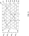
- the one or more local limits 586 may include a carrier band voltage. As shown in FIG.
- a first carrier wave signal 612 is located within a first carrier band voltage 622 defined by a first voltage level 632 and a second voltage level 634
- a second carrier wave signal 614 is located within a second carrier band voltage 624 defined by the second voltage level 634 and a third voltage level 636
- a third carrier wave signal 616 is located within a third carrier band voltage 626 defined by the third voltage level 636 and a fourth voltage level 638
- a fourth carrier wave signal 618 is located within a fourth carrier band voltage 628 defined by the fourth voltage level 638 and a fifth voltage level 642.
- the local limit 586 is set to ensure the three-phase voltage modulation signals 610, 620, 630 modified by the CMV signal will fall within the respective first, third, fourth carrier band voltages 622, 626, 628.
- the local limit 586 is set to ensure the three-phase voltage modulation signals 610 modified by the CMV signal fall within the respective carrier band voltages 622, 626, and 628.
- applying the local limits to three-phase voltage commands at any instant may generate three different maximum CMV limits and three different minimum CMV limits.
- the maximum CMV limit 524 may be the one that is a minimum of the three different maximum CMV limits
- the minimum CMV limit 526 is the one that is a maximum of the three different minimum CMV limits. It can be understood that using the local limits such as carrier band voltage to generate the maximum and minimum CMV limits can avoid the creation of additional switching patterns and transients. As a result, control complexity of the controller for controlling the switching of the power converters can be reduced. In addition, switching loss can be reduced by keeping the one or more command voltages or modulation voltages after CMV injection within their original carrier band voltages.
- FIG. 12 is a flowchart illustrating a common mode voltage injection method.
- the CMV injection method 800 may be independently implemented by the second CMV injection module 404 shown in FIGS. 6-8 to achieve balancing DC voltage present at a DC link of the power conversion system 100.
- the common mode voltage injection method 800 may also be implemented in combination with the first CMV injection module 402 to achieve multiple functions in association with the operation of the power conversion system 100.
- At least some of the blocks/actions illustrated in method 800 may be programmed with software instructions stored in a computer-readable storage medium.
- the computer-readable storage medium may include volatile and nonvolatile, removable and non-removable media implemented in any method or technology.
- the computer-readable storage medium includes, but is not limited to, RAM, ROM, EEPROM, flash memory or other memory technology, CD-ROM, digital versatile disks (DVD) or other optical storage, magnetic cassettes, magnetic tape, magnetic disk storage or other magnetic storage devices, or any other non-transitory medium which can be used to store the desired information and which can be accessed by one or more processors.
- the method 800 includes a block 802, in which one or more voltage commands such as three-phase AC voltage commands are obtained.
- the one or more voltage commands or the three-phase AC voltage commands may be obtained from one or more upper level controllers by implementing one or more algorithms to achieve a desired AC voltage at the output of the power converter.
- the one or more voltage commands may be signals that are free of CMV injection.
- the one or more voltage commands may have already been modified by a first CMV signal which may be generated through min-max calculation or has pure third-order harmonic signal as described above with reference to FIG. 6 .
- the method 800 continues to classify the obtained one or more voltage commands.
- a min-max classifier 506 may be used to identify a maximum voltage command, a medium voltage command and a minimum voltage command from the three-phase AC voltage commands at each instantaneous time.
- the method 800 continues to calculate a maximum CMV limit and a minimum CMV limit based at least in part on the instantaneous maximum and minimum voltage commands using one or more criteria.
- the one or more criteria may include one or more global limits such as one or more DC link voltage limits. More specifically, the maximum CMV limit is generated to ensure that the one or more voltage commands modified by the CMV injection signal will not exceed an upper DC link voltage. Similarly, the minimum CMV limit is generated to ensure the one or more voltage commands modified by the CMV injection signal will not exceed a lower DC link voltage.
- the maximum or minimum CMV limits are generated in a manner that the one or more voltage commands after CMV injection signal doesn't change signs.
- the one or more criteria may include one or more local limits such as one or more carrier band voltages.
- the maximum CMV limit and the minimum CMV limit are generated to ensure that the one or more command voltages after CMV injection do not jump from one carrier band voltage to another carrier band voltage. Therefore, additional switching patterns and/or transients can be avoided, and control complexity and switching loss can be reduced.
- the method 800 continues to calculate NP currents after CMV injection based on the maximum CMV limit and the minimum CMV limit.
- the calculation of the NP currents can be done in analytical and/or numerical manners.
- the calculated NP currents are scanned to find out the maximum and minimum NP currents and CMVs corresponding to the maximum and minimum NP currents. Redundant switching states may be taken into consideration in generation of the maximum and minimum NP currents so as to achieve certain functions such as reducing voltage stress on flying capacitors of the power converter.
- the method 800 continues to calculate a reference NP current based at least in part on an original NP current, the maximum and minimum NP currents, and a gain signal.
- the calculation of the reference NP current depends on a desired current pattern present at an NP of the DC link. For example, when the power conversion system is operated under a first NP current regulation mode, in which the original AC unbalance at the NP of the DC link should be kept. In this case, the original NP current may include a third-order harmonic current signal. sIn addition, a big change of the PWM pattern can be avoided, such that THD of the output AC voltage can be minimized.
- the power conversion system is operated under a second NP current regulation mode, in which the AC unbalance should be removed or reduced. In this case, the original NP current may be set to be zero.
- the gain signal is generated by a DC link voltage balance controller by regulating input signals representing voltage difference between at least two DC capacitors of the DC link.
- the method 800 continues to calculate a CMV injection signal based at least in part on the calculated reference NP current.
- a reverse function such as one or more linear functions of the CMV in terms of NP current can be derived for calculation of the CMV injection signals.
- a lookup table may be used to find the CMV injection signal corresponding to the reference NP current.
- the one or more voltage commands obtained at block 802 is modified by combining the reference CMV injection signal with the one or more voltage commands.
- the modified one or more voltage commands are supplied to a modulator for generating control signals used to turn on and/or off the various switching devices in the power converter. Therefore, the voltage difference at the DC link can be minimized by injecting the CMV signals to the one or more voltage commands or modulation signals.
- the method 800 includes blocks for obtaining three-phase AC current commands which are used to calculate the original NP current at the NP of the DC link.
- the method 800 also includes blocks for identifying an instantaneous maximum current command, an instantaneous medium current command and an instantaneous minimum current command from the three-phase AC current commands.
- the original NP current is calculated using the instantaneous maximum, medium and minimum current commands, and also using the maximum, medium and minimum voltage commands identified in block 804.
Landscapes
- Engineering & Computer Science (AREA)
- Power Engineering (AREA)
- Inverter Devices (AREA)
Claims (2)
- Système de conversion de puissance (100), comprenant :une liaison en courant continu CC (124) comprenant un premier condensateur en CC (242) et un second condensateur en CC (246) électriquement couplés en série et définissant un point neutre NP en CC (252) entre ces derniers ;au moins un convertisseur de puissance à multiples niveaux (126 ; 200 ; 300) ; etune unité de commande (140) couplée à l'au moins un convertisseur de puissance à multiples niveaux (126), l'unité de commande (140) comprenant un module d'injection (404; 500; 600) de tension de mode commun CMV conçu pour produire un signal CMV (408; 564) pour modifier au moins une tension d'ordre (422; 424) pour réguler la composante de courant CC ou CA s'écoulant depuis le NP en CC (252) de la liaison en CC (124) afin de réduire la différence de tension entre les premier et second condensateurs en CC (242, 244) sensiblement à zéro ;le module d'injection de CMV (404 ; 500; 600) comprenant :un classificateur mini-maxi (506) conçu pour déterminer un ordre de tension maximale instantanée (508), un ordre de tension intermédiaire instantanée (509) et un ordre de tension minimale instantanée (512) à partir d'ordres de tension en CA à trois phases (504), et pour déterminer un ordre de courant maximal instantané (516), un ordre de courant intermédiaire instantané (515) et un ordre de courant minimal instantané (514) à partir d'ordres de courant CA à trois phases (502) ;un calculateur de limite de CMV (518) conçu pour calculer une limite de CMV maximale (524) et une limite de CMV minimale (526) sur la base des ordres de tension maximale et minimale instantanée (508, 512) et de l'un d'un signal de limite globale (522) et d'un signal de limite locale (586) ;un calculateur de courant de NP (528) conçu pour calculer un courant de NP maximal (538), un courant de NP minimal (542), une CMV maximale (534) correspondant au courant de NP maximal (538) et une CMV minimale (536) correspondant au courant de NP minimal (542) sur la base au moins en partie de la limite de CMV maximale (524) et de la limite de CMV minimale (526) ;un pré-calculateur de courant de NP (544) conçu pour calculer un premier signal de courant de NP original (546) s'écoulant depuis ou vers le NP en CC (252) de la liaison en CC (124) sur la base au moins en partie des ordres de tension maximale, intermédiaire et minimale instantanée (508, 509, 512) et des ordres de courant maximal, intermédiaire et minimal instantané (514, 515, 516) ;une unité de sélection de courant (548) conçue pour sélectionner l'un du premier signal de courant de NP original (546) et d'un second signal de courant de NP original (552) en fonction de différents modes de régulation de courant de NP du système de conversion de puissance (100), dans laquelle l'unité de sélection de courant (548) est configurée pour être mise en œuvre selon un signal de sélection de mode (551) pour sélectionner le premier signal de courant de NP original (546) quand le système de conversion de puissance (100) doit être mis en œuvre sous un premier mode de régulation de NP dans lequel un courant harmonique de troisième ordre présent au niveau du NP en CC (252) de la liaison en CC (124) devrait être maintenu, et pour être mise en œuvre selon un signal de sélection de mode mis à jour (551) pour sélectionner le second signal de courant de NP original (552) quand le système de conversion de puissance (100) doit être mis en œuvre sous un second mode de régulation de NP dans lequel des fluctuations de courant harmonique de troisième ordre présentes au niveau du NP en CC (252) de la liaison en CC (124) devraient être réduites ou supprimées ;un calculateur de courant de NP de référence (556) conçu pour calculer un courant de NP de référence (558) sur la base au moins en partie des courants de NP maximal et minimal (538, 542), d'un signal de gain (584) et du signal sélectionné des premier et second signaux de courant de NP originaux (546, 552) ;un régulateur d'équilibre de tension en CC (582) conçu pour produire le signal de gain (584) sur la base au moins en partie d'un signal de différence de tension en CC (574) au niveau de la liaison en CC (124) ; etun calculateur de fonction inverse (562) conçu pour calculer le signal de CMV (564) sur la base au moins en partie des courants de NP maximal et minimal (538, 542), des CMV maximale et minimale (534, 536) et du courant de NP de référence (558).
- Procédé de mise en œuvre d'un système de conversion de puissance (100), comprenant :une liaison en courant continu CC (124) comprenant un premier condensateur en CC (242) et un second condensateur en CC (246) électriquement couplés en série et définissant un point neutre NP en CC (252) entre ces derniers ; etau moins un convertisseur de puissance à multiples niveaux (126 ; 200 ; 300) ;le procédé comprenant :la production d'un signal de CMV (408 ; 564) pour modifier au moins un ordre de tension (422 ; 424) pour réguler la composante de courant en CC ou CA s'écoulant depuis ou vers le NP en CC (252) de la liaison en CC (124) afin de réduire la différence de tension entre les premier et second condensateurs en CC (242, 244) sensiblement à zéro ;le procédé comprenant en outre :la détermination d'un ordre de tension maximale instantanée (508), d'un ordre de tension intermédiaire instantanée (509) et d'un ordre de tension minimale instantanée (512) à partir d'ordres de tension en CA à trois phases (504), et la détermination d'un ordre de courant maximal instantané (516), d'un ordre de courant intermédiaire instantané (515) et d'un ordre de courant minimal instantané (514) à partir d'ordres de courant en CA à trois phases (502) ;le calcul d'une limite de CMV maximale (524) et d'une limite de CMV minimale (526) sur la base des ordres de tension maximale et minimale instantanée (508, 512) et de l'un d'un signal de limite globale (522) et d'un signal de limite locale (586) ;le calcul d'un courant de NP maximal (538), d'un courant de NP minimal (542), d'une CMV maximale (534) correspondant au courant de NP maximal (538) et d'une CMV minimale (536) correspondant au courant de NP minimal (542) sur la base au moins en partie de la limite de CMV maximale (524) et de la limite de CMV minimale (526) ;le calcul d'un premier signal de courant de NP original (546) s'écoulant depuis ou vers le NP en CC (252) de la liaison en CC (124) sur la base au moins en partie des ordres de tension maximale, intermédiaire et minimale instantanée (508, 509, 512) et des ordres de courant maximal, intermédiaire et minimal instantané (514, 515, 516) ;la sélection de l'un du premier signal de courant de NP original (546) et d'un second signal de courant de NP original (552) en fonction de différents modes de régulation de courant de NP du système de conversion de puissance (100), dans lequel le premier signal de courant de NP original (546) est sélectionné quand le système de conversion de puissance (100) doit être mis en œuvre sous un premier mode de régulation de NP dans lequel un courant harmonique de troisième ordre présent au niveau du NP en CC (252) de la liaison en CC (124) devrait être maintenu, et le second signal de courant de NP original (552) est sélectionné quand le système de conversion de puissance (100) doit être mis en œuvre sous un second mode de régulation de NP dans lequel des fluctuations de courant harmonique de troisième ordre présentes au niveau du NP en CC (252) de la liaison en CC (124) devraient être réduites ou supprimées ;le calcul d'un courant de NP de référence (558) sur la base au moins en partie des courants de NP maximal et minimal (538, 542), d'un signal de gain (584) et du signal sélectionné des premier et second signaux de courant de NP originaux (546, 552) ;la production du signal de gain (584) sur la base au moins en partie d'un signal de différence de tension en CC (574) au niveau de la liaison en CC (124) ; etle calcul du signal de CMV (564) sur la base au moins en partie des courants de NP maximal et minimal (538, 542), des CMV maximale et minimale (534, 536) et du courant de NP de référence (558).
Applications Claiming Priority (1)
| Application Number | Priority Date | Filing Date | Title |
|---|---|---|---|
| CN201310276169.5A CN104283432B (zh) | 2013-07-03 | 2013-07-03 | 联合共模电压注入系统和方法 |
Publications (2)
| Publication Number | Publication Date |
|---|---|
| EP2827490A1 EP2827490A1 (fr) | 2015-01-21 |
| EP2827490B1 true EP2827490B1 (fr) | 2021-01-20 |
Family
ID=51033033
Family Applications (1)
| Application Number | Title | Priority Date | Filing Date |
|---|---|---|---|
| EP14175253.5A Active EP2827490B1 (fr) | 2013-07-03 | 2014-07-01 | Système et procédé d'injection de tension de mode commun |
Country Status (6)
| Country | Link |
|---|---|
| US (1) | US9634576B2 (fr) |
| EP (1) | EP2827490B1 (fr) |
| CN (1) | CN104283432B (fr) |
| BR (1) | BR102014016439A2 (fr) |
| CA (1) | CA2855310A1 (fr) |
| ES (1) | ES2861954T3 (fr) |
Families Citing this family (26)
| Publication number | Priority date | Publication date | Assignee | Title |
|---|---|---|---|---|
| US9755545B2 (en) * | 2014-11-21 | 2017-09-05 | General Electric Company | System and method for unified common mode voltage injection |
| CN106341050A (zh) * | 2015-07-17 | 2017-01-18 | 台达电子企业管理(上海)有限公司 | 多电平变频器及多电平变频器的控制方法 |
| KR102485705B1 (ko) * | 2016-02-18 | 2023-01-05 | 엘에스일렉트릭(주) | 멀티 레벨 인버터의 3상 평형 전압 제어 방법 |
| US9970417B2 (en) * | 2016-04-14 | 2018-05-15 | General Electric Company | Wind converter control for weak grid |
| CN107689735B (zh) * | 2016-08-05 | 2020-01-31 | 台达电子企业管理(上海)有限公司 | 功率变换系统及其共模电压抑制方法 |
| CN106533236B (zh) * | 2016-12-15 | 2018-10-16 | 电子科技大学 | 一种三电平逆变器的最小开关损耗实现方法 |
| CN106981976B (zh) * | 2017-03-24 | 2019-08-20 | 江苏固德威电源科技股份有限公司 | T型三电平三相逆变器抑制中线共模电流的方法 |
| EP3393034A1 (fr) * | 2017-04-21 | 2018-10-24 | GE Energy Power Conversion Technology Limited | Commande d'un convertisseur à trois niveaux dos à dos avec compensation des ondulations de tension du point milieu |
| CN107517018B (zh) * | 2017-08-25 | 2020-03-27 | 上海蓝瑞电气有限公司 | 适用于三电平逆变器的pwm调制方法 |
| US11329500B2 (en) * | 2019-01-30 | 2022-05-10 | Industrial Technology Research Institute | Charging and discharging device and charging and discharging method |
| EP3836381A1 (fr) * | 2019-12-11 | 2021-06-16 | ABB Schweiz AG | Commande de convertisseur npc utilisant une injection d'harmoniques de tension |
| US20230299692A1 (en) * | 2020-09-28 | 2023-09-21 | Mitsubishi Electric Corporation | Power converter |
| CN112531722B (zh) * | 2020-12-01 | 2022-12-13 | 中国电力科学研究院有限公司 | 一种无功电压控制方法及系统 |
| EP4024694A1 (fr) * | 2020-12-30 | 2022-07-06 | Siemens Aktiengesellschaft | Module de condensateur volant et onduleur multiniveau |
| CN114977862B (zh) * | 2021-02-24 | 2026-03-24 | 华为数字能源技术有限公司 | 一种共模电压调整方法、装置及控制系统 |
| CN113098306B (zh) * | 2021-03-30 | 2022-06-17 | 北京交通大学 | 五电平及多电平层叠式多单元变换器调制控制方法 |
| CN112865575B (zh) * | 2021-04-13 | 2022-05-24 | 阳光电源股份有限公司 | 一种逆变控制方法及其应用装置 |
| EP4315582A1 (fr) * | 2021-04-15 | 2024-02-07 | Huawei Technologies Co., Ltd. | Convertisseur de puissance matriciel et procédé d'utilisation dans le convertisseur de puissance matriciel |
| CN113162450B (zh) * | 2021-05-07 | 2022-12-02 | 山东大学 | 一种基于共模电压注入的五电平逆变器调制方法 |
| CN114460409B (zh) * | 2022-04-13 | 2022-06-21 | 广东电网有限责任公司佛山供电局 | 基于中性点不平衡数据的电容器监测方法、装置及设备 |
| CA3264574A1 (fr) * | 2022-08-11 | 2024-02-15 | Smartd Technologies Inc. | Modulation sans capteur à porteuse unique à fréquence constante pour le convertisseur multicellulaire à condensateur volant à trois niveaux |
| CN115589013B (zh) * | 2022-11-10 | 2025-05-13 | 桂林星辰科技股份有限公司 | 一种错峰用电的双向dcdc电池管理装置及其控制方法 |
| CN115589169B (zh) * | 2022-12-13 | 2023-04-07 | 麦田能源有限公司 | 基于瞬时特性的逆变器的控制方法、装置及逆变器系统 |
| FR3144896A1 (fr) * | 2023-01-10 | 2024-07-12 | Supergrid Institute | système de transfert de puissance pour piloter économiquement une machine électrique et la connecter à un système de stockage d’énergie |
| US12346184B2 (en) * | 2023-01-19 | 2025-07-01 | General Electric Company | Reduced common mode voltage pulse width modulation switching scheme with capacitor voltage balancing for a multilevel power converter |
| CN120710359B (zh) * | 2025-09-01 | 2025-11-07 | 成都森未科技有限公司 | 一种飞跨电容型直流升压变换器与光伏系统 |
Family Cites Families (11)
| Publication number | Priority date | Publication date | Assignee | Title |
|---|---|---|---|---|
| EP1253706B1 (fr) | 2001-04-25 | 2013-08-07 | ABB Schweiz AG | Circuit d'électronique de puissane et procédé pour transférer la puissance active |
| FR2901074B1 (fr) | 2006-05-09 | 2008-06-13 | Schneider Electric Ind Sas | Dispositif et procede de commande d'un convertisseur et conversisseur electrique comportant un tel dispositif |
| US7573732B2 (en) | 2007-05-25 | 2009-08-11 | General Electric Company | Protective circuit and method for multi-level converter |
| US7920393B2 (en) | 2007-06-01 | 2011-04-05 | Drs Power & Control Technologies, Inc. | Four pole neutral-point clamped three phase converter with low common mode voltage output |
| US7952896B2 (en) | 2008-08-20 | 2011-05-31 | Hamilton Sundstrand Corporation | Power conversion architecture with zero common mode voltage |
| CN102577073B (zh) | 2009-09-04 | 2015-05-20 | Abb技术有限公司 | 计算用于模块化多电平转换器的插入指数的方法和装置 |
| CN102823122B (zh) | 2010-04-15 | 2016-01-20 | Abb研究有限公司 | 具有第二和第三阶谐波降低滤波器的模块化多级功率转换器 |
| US8441820B2 (en) * | 2010-09-29 | 2013-05-14 | General Electric Company | DC-link voltage balancing system and method for multilevel converters |
| US8319466B2 (en) | 2011-02-21 | 2012-11-27 | Rockwell Automation Technologies, Inc. | Modular line-to-ground fault identification |
| FR2975549B1 (fr) | 2011-05-17 | 2015-01-02 | Converteam Technology Ltd | Onduleur de tension a 2n+1 niveaux |
| CN103138594B (zh) | 2011-11-22 | 2016-03-02 | 通用电气公司 | 中点箝位式变流器的控制系统及控制方法及补偿控制单元 |
-
2013
- 2013-07-03 CN CN201310276169.5A patent/CN104283432B/zh active Active
-
2014
- 2014-06-26 CA CA2855310A patent/CA2855310A1/fr not_active Abandoned
- 2014-06-27 US US14/317,361 patent/US9634576B2/en active Active
- 2014-07-01 EP EP14175253.5A patent/EP2827490B1/fr active Active
- 2014-07-01 ES ES14175253T patent/ES2861954T3/es active Active
- 2014-07-02 BR BR102014016439A patent/BR102014016439A2/pt not_active IP Right Cessation
Non-Patent Citations (2)
| Title |
|---|
| KONSTANTINOU G ET AL: "The seven-level flying capacitor based ANPC converter for grid intergration of utility-scale PV systems", POWER ELECTRONICS FOR DISTRIBUTED GENERATION SYSTEMS (PEDG), 2012 3RD IEEE INTERNATIONAL SYMPOSIUM ON, IEEE, 25 June 2012 (2012-06-25), pages 592 - 597, XP032226622, ISBN: 978-1-4673-2021-4, DOI: 10.1109/PEDG.2012.6254062 * |
| KUI WANG ET AL: "DC-Link Voltage Balancing Method with Reduced Common- Mode Voltage for a Five-Level ANPC Inverter", PRZEGLAD ELEKTROTECHNICZNY, 1 March 2013 (2013-03-01), Warszawa, pages 32 - 34, XP055528227, Retrieved from the Internet <URL:http://pe.org.pl/articles/2013/3b/11.pdf> [retrieved on 20181128] * |
Also Published As
| Publication number | Publication date |
|---|---|
| BR102014016439A2 (pt) | 2015-12-08 |
| CN104283432B (zh) | 2017-12-26 |
| EP2827490A1 (fr) | 2015-01-21 |
| US9634576B2 (en) | 2017-04-25 |
| CN104283432A (zh) | 2015-01-14 |
| US20150008750A1 (en) | 2015-01-08 |
| CA2855310A1 (fr) | 2015-01-03 |
| ES2861954T3 (es) | 2021-10-06 |
Similar Documents
| Publication | Publication Date | Title |
|---|---|---|
| EP2827490B1 (fr) | Système et procédé d'injection de tension de mode commun | |
| US9755545B2 (en) | System and method for unified common mode voltage injection | |
| Najafi et al. | Design and implementation of a new multilevel inverter topology | |
| Tarisciotti et al. | Active DC voltage balancing PWM technique for high-power cascaded multilevel converters | |
| Yaragatti | Design and implementation of active neutral-point-clamped nine-level reduced device count inverter: an application to grid integrated renewable energy sources. | |
| US9048754B2 (en) | System and method for offsetting the input voltage unbalance in multilevel inverters or the like | |
| DK201470472A1 (en) | Power conversion system and method | |
| Zeng et al. | Novel single-phase five-level voltage-source inverter for the shunt active power filter | |
| Ahmadzadeh et al. | Modified PWM control method for neutral point clamped multilevel inverters | |
| Pawar et al. | Notice of Violation of IEEE Publication Principles: Modular multilevel converters: A review on topologies, modulation, modeling and control schemes | |
| Naik et al. | A new two-phase five-level converter for three-phase isolated grid-tied systems with inherent capacitor balancing and reduced component count | |
| Metri et al. | Model predictive control for the packed U-Cells 7-level grid connected inverter | |
| Jakka et al. | A triple port active bridge converter based multi-fed power electronic transformer | |
| Raju et al. | Nearly constant switching frequency hysteresis current controller for multilevel inverter based STATCOM | |
| Mei et al. | Quasi-fixed-frequency hysteresis current tracking control strategy for modular multilevel converters | |
| US20150091488A1 (en) | Method and system for driving electric machines | |
| Jayan et al. | Cascaded dual output multilevel converter to enhance power delivery and quality | |
| Hussein et al. | Improved phase disposition pulse width modulation for a modified cascaded dual-output multilevel converter | |
| Cortes et al. | Predictive control of a grid-connected cascaded H-bridge multilevel converter | |
| Zaimeddine et al. | Direct power control strategies of a grid-connected three-level voltage source converter VSI-NPC | |
| Kang et al. | A carrier-based pwm method with the double frequency voltage injection for three-level neutral-point clamped (NPC) converters | |
| Sabyasachi et al. | A 13-level hybrid multilevel inverter topology by combining ANPC and improved H-bridge | |
| Li et al. | A harmonic constrained minimum energy controller for a single-phase grid-tied inverter using model predictive control | |
| Abootorabi et al. | A new switching method for multi-level asymmetric CHB to reduce THD and torque ripple in IM drive | |
| Hosseinpour et al. | Design and control of three-phase quasi-Z-source based hybrid 2/3 level inverter |
Legal Events
| Date | Code | Title | Description |
|---|---|---|---|
| 17P | Request for examination filed |
Effective date: 20140701 |
|
| AK | Designated contracting states |
Kind code of ref document: A1 Designated state(s): AL AT BE BG CH CY CZ DE DK EE ES FI FR GB GR HR HU IE IS IT LI LT LU LV MC MK MT NL NO PL PT RO RS SE SI SK SM TR |
|
| AX | Request for extension of the european patent |
Extension state: BA ME |
|
| PUAI | Public reference made under article 153(3) epc to a published international application that has entered the european phase |
Free format text: ORIGINAL CODE: 0009012 |
|
| RIN1 | Information on inventor provided before grant (corrected) |
Inventor name: YANG, SHUITAO Inventor name: CHEN, KUNLUN Inventor name: QU, BO Inventor name: SCHROEDER, STEFAN Inventor name: SHEN, JIE |
|
| RIN1 | Information on inventor provided before grant (corrected) |
Inventor name: CHEN, KUNLUN Inventor name: QU, BO Inventor name: SCHROEDER, STEFAN Inventor name: YANG, SHUITAO Inventor name: SHEN, JIE |
|
| R17P | Request for examination filed (corrected) |
Effective date: 20150629 |
|
| RBV | Designated contracting states (corrected) |
Designated state(s): AL AT BE BG CH CY CZ DE DK EE ES FI FR GB GR HR HU IE IS IT LI LT LU LV MC MK MT NL NO PL PT RO RS SE SI SK SM TR |
|
| STAA | Information on the status of an ep patent application or granted ep patent |
Free format text: STATUS: EXAMINATION IS IN PROGRESS |
|
| 17Q | First examination report despatched |
Effective date: 20181205 |
|
| GRAP | Despatch of communication of intention to grant a patent |
Free format text: ORIGINAL CODE: EPIDOSNIGR1 |
|
| STAA | Information on the status of an ep patent application or granted ep patent |
Free format text: STATUS: GRANT OF PATENT IS INTENDED |
|
| INTG | Intention to grant announced |
Effective date: 20200811 |
|
| GRAS | Grant fee paid |
Free format text: ORIGINAL CODE: EPIDOSNIGR3 |
|
| GRAA | (expected) grant |
Free format text: ORIGINAL CODE: 0009210 |
|
| STAA | Information on the status of an ep patent application or granted ep patent |
Free format text: STATUS: THE PATENT HAS BEEN GRANTED |
|
| AK | Designated contracting states |
Kind code of ref document: B1 Designated state(s): AL AT BE BG CH CY CZ DE DK EE ES FI FR GB GR HR HU IE IS IT LI LT LU LV MC MK MT NL NO PL PT RO RS SE SI SK SM TR |
|
| REG | Reference to a national code |
Ref country code: GB Ref legal event code: FG4D |
|
| REG | Reference to a national code |
Ref country code: CH Ref legal event code: EP |
|
| REG | Reference to a national code |
Ref country code: DE Ref legal event code: R096 Ref document number: 602014074342 Country of ref document: DE |
|
| REG | Reference to a national code |
Ref country code: AT Ref legal event code: REF Ref document number: 1357218 Country of ref document: AT Kind code of ref document: T Effective date: 20210215 |
|
| REG | Reference to a national code |
Ref country code: IE Ref legal event code: FG4D |
|
| REG | Reference to a national code |
Ref country code: NO Ref legal event code: T2 Effective date: 20210120 |
|
| REG | Reference to a national code |
Ref country code: NL Ref legal event code: MP Effective date: 20210120 |
|
| REG | Reference to a national code |
Ref country code: LT Ref legal event code: MG9D |
|
| REG | Reference to a national code |
Ref country code: AT Ref legal event code: MK05 Ref document number: 1357218 Country of ref document: AT Kind code of ref document: T Effective date: 20210120 |
|
| PG25 | Lapsed in a contracting state [announced via postgrant information from national office to epo] |
Ref country code: NL Free format text: LAPSE BECAUSE OF FAILURE TO SUBMIT A TRANSLATION OF THE DESCRIPTION OR TO PAY THE FEE WITHIN THE PRESCRIBED TIME-LIMIT Effective date: 20210120 Ref country code: BG Free format text: LAPSE BECAUSE OF FAILURE TO SUBMIT A TRANSLATION OF THE DESCRIPTION OR TO PAY THE FEE WITHIN THE PRESCRIBED TIME-LIMIT Effective date: 20210420 Ref country code: PT Free format text: LAPSE BECAUSE OF FAILURE TO SUBMIT A TRANSLATION OF THE DESCRIPTION OR TO PAY THE FEE WITHIN THE PRESCRIBED TIME-LIMIT Effective date: 20210520 Ref country code: LT Free format text: LAPSE BECAUSE OF FAILURE TO SUBMIT A TRANSLATION OF THE DESCRIPTION OR TO PAY THE FEE WITHIN THE PRESCRIBED TIME-LIMIT Effective date: 20210120 Ref country code: FI Free format text: LAPSE BECAUSE OF FAILURE TO SUBMIT A TRANSLATION OF THE DESCRIPTION OR TO PAY THE FEE WITHIN THE PRESCRIBED TIME-LIMIT Effective date: 20210120 Ref country code: GR Free format text: LAPSE BECAUSE OF FAILURE TO SUBMIT A TRANSLATION OF THE DESCRIPTION OR TO PAY THE FEE WITHIN THE PRESCRIBED TIME-LIMIT Effective date: 20210421 Ref country code: HR Free format text: LAPSE BECAUSE OF FAILURE TO SUBMIT A TRANSLATION OF THE DESCRIPTION OR TO PAY THE FEE WITHIN THE PRESCRIBED TIME-LIMIT Effective date: 20210120 |
|
| PG25 | Lapsed in a contracting state [announced via postgrant information from national office to epo] |
Ref country code: AT Free format text: LAPSE BECAUSE OF FAILURE TO SUBMIT A TRANSLATION OF THE DESCRIPTION OR TO PAY THE FEE WITHIN THE PRESCRIBED TIME-LIMIT Effective date: 20210120 Ref country code: PL Free format text: LAPSE BECAUSE OF FAILURE TO SUBMIT A TRANSLATION OF THE DESCRIPTION OR TO PAY THE FEE WITHIN THE PRESCRIBED TIME-LIMIT Effective date: 20210120 Ref country code: LV Free format text: LAPSE BECAUSE OF FAILURE TO SUBMIT A TRANSLATION OF THE DESCRIPTION OR TO PAY THE FEE WITHIN THE PRESCRIBED TIME-LIMIT Effective date: 20210120 Ref country code: RS Free format text: LAPSE BECAUSE OF FAILURE TO SUBMIT A TRANSLATION OF THE DESCRIPTION OR TO PAY THE FEE WITHIN THE PRESCRIBED TIME-LIMIT Effective date: 20210120 Ref country code: SE Free format text: LAPSE BECAUSE OF FAILURE TO SUBMIT A TRANSLATION OF THE DESCRIPTION OR TO PAY THE FEE WITHIN THE PRESCRIBED TIME-LIMIT Effective date: 20210120 |
|
| PG25 | Lapsed in a contracting state [announced via postgrant information from national office to epo] |
Ref country code: IS Free format text: LAPSE BECAUSE OF FAILURE TO SUBMIT A TRANSLATION OF THE DESCRIPTION OR TO PAY THE FEE WITHIN THE PRESCRIBED TIME-LIMIT Effective date: 20210520 |
|
| REG | Reference to a national code |
Ref country code: ES Ref legal event code: FG2A Ref document number: 2861954 Country of ref document: ES Kind code of ref document: T3 Effective date: 20211006 |
|
| REG | Reference to a national code |
Ref country code: DE Ref legal event code: R097 Ref document number: 602014074342 Country of ref document: DE |
|
| PG25 | Lapsed in a contracting state [announced via postgrant information from national office to epo] |
Ref country code: SM Free format text: LAPSE BECAUSE OF FAILURE TO SUBMIT A TRANSLATION OF THE DESCRIPTION OR TO PAY THE FEE WITHIN THE PRESCRIBED TIME-LIMIT Effective date: 20210120 Ref country code: EE Free format text: LAPSE BECAUSE OF FAILURE TO SUBMIT A TRANSLATION OF THE DESCRIPTION OR TO PAY THE FEE WITHIN THE PRESCRIBED TIME-LIMIT Effective date: 20210120 Ref country code: CZ Free format text: LAPSE BECAUSE OF FAILURE TO SUBMIT A TRANSLATION OF THE DESCRIPTION OR TO PAY THE FEE WITHIN THE PRESCRIBED TIME-LIMIT Effective date: 20210120 |
|
| PLBE | No opposition filed within time limit |
Free format text: ORIGINAL CODE: 0009261 |
|
| STAA | Information on the status of an ep patent application or granted ep patent |
Free format text: STATUS: NO OPPOSITION FILED WITHIN TIME LIMIT |
|
| PG25 | Lapsed in a contracting state [announced via postgrant information from national office to epo] |
Ref country code: DK Free format text: LAPSE BECAUSE OF FAILURE TO SUBMIT A TRANSLATION OF THE DESCRIPTION OR TO PAY THE FEE WITHIN THE PRESCRIBED TIME-LIMIT Effective date: 20210120 Ref country code: RO Free format text: LAPSE BECAUSE OF FAILURE TO SUBMIT A TRANSLATION OF THE DESCRIPTION OR TO PAY THE FEE WITHIN THE PRESCRIBED TIME-LIMIT Effective date: 20210120 Ref country code: SK Free format text: LAPSE BECAUSE OF FAILURE TO SUBMIT A TRANSLATION OF THE DESCRIPTION OR TO PAY THE FEE WITHIN THE PRESCRIBED TIME-LIMIT Effective date: 20210120 |
|
| 26N | No opposition filed |
Effective date: 20211021 |
|
| PG25 | Lapsed in a contracting state [announced via postgrant information from national office to epo] |
Ref country code: AL Free format text: LAPSE BECAUSE OF FAILURE TO SUBMIT A TRANSLATION OF THE DESCRIPTION OR TO PAY THE FEE WITHIN THE PRESCRIBED TIME-LIMIT Effective date: 20210120 |
|
| PG25 | Lapsed in a contracting state [announced via postgrant information from national office to epo] |
Ref country code: SI Free format text: LAPSE BECAUSE OF FAILURE TO SUBMIT A TRANSLATION OF THE DESCRIPTION OR TO PAY THE FEE WITHIN THE PRESCRIBED TIME-LIMIT Effective date: 20210120 |
|
| REG | Reference to a national code |
Ref country code: CH Ref legal event code: PL |
|
| GBPC | Gb: european patent ceased through non-payment of renewal fee |
Effective date: 20210701 |
|
| PG25 | Lapsed in a contracting state [announced via postgrant information from national office to epo] |
Ref country code: MC Free format text: LAPSE BECAUSE OF FAILURE TO SUBMIT A TRANSLATION OF THE DESCRIPTION OR TO PAY THE FEE WITHIN THE PRESCRIBED TIME-LIMIT Effective date: 20210120 |
|
| REG | Reference to a national code |
Ref country code: BE Ref legal event code: MM Effective date: 20210731 |
|
| PG25 | Lapsed in a contracting state [announced via postgrant information from national office to epo] |
Ref country code: LI Free format text: LAPSE BECAUSE OF NON-PAYMENT OF DUE FEES Effective date: 20210731 Ref country code: GB Free format text: LAPSE BECAUSE OF NON-PAYMENT OF DUE FEES Effective date: 20210701 Ref country code: CH Free format text: LAPSE BECAUSE OF NON-PAYMENT OF DUE FEES Effective date: 20210731 |
|
| PG25 | Lapsed in a contracting state [announced via postgrant information from national office to epo] |
Ref country code: IS Free format text: LAPSE BECAUSE OF FAILURE TO SUBMIT A TRANSLATION OF THE DESCRIPTION OR TO PAY THE FEE WITHIN THE PRESCRIBED TIME-LIMIT Effective date: 20210520 Ref country code: LU Free format text: LAPSE BECAUSE OF NON-PAYMENT OF DUE FEES Effective date: 20210701 |
|
| PG25 | Lapsed in a contracting state [announced via postgrant information from national office to epo] |
Ref country code: IE Free format text: LAPSE BECAUSE OF NON-PAYMENT OF DUE FEES Effective date: 20210701 Ref country code: BE Free format text: LAPSE BECAUSE OF NON-PAYMENT OF DUE FEES Effective date: 20210731 |
|
| PG25 | Lapsed in a contracting state [announced via postgrant information from national office to epo] |
Ref country code: HU Free format text: LAPSE BECAUSE OF FAILURE TO SUBMIT A TRANSLATION OF THE DESCRIPTION OR TO PAY THE FEE WITHIN THE PRESCRIBED TIME-LIMIT; INVALID AB INITIO Effective date: 20140701 |
|
| PG25 | Lapsed in a contracting state [announced via postgrant information from national office to epo] |
Ref country code: CY Free format text: LAPSE BECAUSE OF FAILURE TO SUBMIT A TRANSLATION OF THE DESCRIPTION OR TO PAY THE FEE WITHIN THE PRESCRIBED TIME-LIMIT Effective date: 20210120 |
|
| REG | Reference to a national code |
Ref country code: NO Ref legal event code: CREP Representative=s name: PLOUGMANN VINGTOFT, C. J. HAMBROS PLASS 2, 0164 Ref country code: NO Ref legal event code: CHAD Owner name: GE ENERGY POWER CONVERSION TECHNOLOGY LIMITED, GB |
|
| PG25 | Lapsed in a contracting state [announced via postgrant information from national office to epo] |
Ref country code: MK Free format text: LAPSE BECAUSE OF FAILURE TO SUBMIT A TRANSLATION OF THE DESCRIPTION OR TO PAY THE FEE WITHIN THE PRESCRIBED TIME-LIMIT Effective date: 20210120 |
|
| REG | Reference to a national code |
Ref country code: DE Ref legal event code: R081 Ref document number: 602014074342 Country of ref document: DE Owner name: GE ENERGY POWER CONVERSION TECHNOLOGY LTD., RU, GB Free format text: FORMER OWNER: GENERAL ELECTRIC COMPANY, SCHENECTADY, NY, US |
|
| REG | Reference to a national code |
Ref country code: ES Ref legal event code: PC2A Owner name: GE ENERGY POWER CONVERSION TECHNOLOGY LIMITED Effective date: 20240718 |
|
| PG25 | Lapsed in a contracting state [announced via postgrant information from national office to epo] |
Ref country code: MT Free format text: LAPSE BECAUSE OF FAILURE TO SUBMIT A TRANSLATION OF THE DESCRIPTION OR TO PAY THE FEE WITHIN THE PRESCRIBED TIME-LIMIT Effective date: 20210120 |
|
| PGFP | Annual fee paid to national office [announced via postgrant information from national office to epo] |
Ref country code: NO Payment date: 20250623 Year of fee payment: 12 |
|
| PGFP | Annual fee paid to national office [announced via postgrant information from national office to epo] |
Ref country code: FR Payment date: 20250620 Year of fee payment: 12 |
|
| PGFP | Annual fee paid to national office [announced via postgrant information from national office to epo] |
Ref country code: ES Payment date: 20250801 Year of fee payment: 12 |
|
| PGFP | Annual fee paid to national office [announced via postgrant information from national office to epo] |
Ref country code: DE Payment date: 20250620 Year of fee payment: 12 |
|
| PGFP | Annual fee paid to national office [announced via postgrant information from national office to epo] |
Ref country code: IT Payment date: 20250619 Year of fee payment: 12 |
|
| PG25 | Lapsed in a contracting state [announced via postgrant information from national office to epo] |
Ref country code: TR Free format text: LAPSE BECAUSE OF FAILURE TO SUBMIT A TRANSLATION OF THE DESCRIPTION OR TO PAY THE FEE WITHIN THE PRESCRIBED TIME-LIMIT Effective date: 20210120 |