EP2879196A1 - Light emitting element material and light emitting element - Google Patents
Light emitting element material and light emitting element Download PDFInfo
- Publication number
- EP2879196A1 EP2879196A1 EP13823334.1A EP13823334A EP2879196A1 EP 2879196 A1 EP2879196 A1 EP 2879196A1 EP 13823334 A EP13823334 A EP 13823334A EP 2879196 A1 EP2879196 A1 EP 2879196A1
- Authority
- EP
- European Patent Office
- Prior art keywords
- group
- light
- compound
- emitting device
- general formula
- Prior art date
- Legal status (The legal status is an assumption and is not a legal conclusion. Google has not performed a legal analysis and makes no representation as to the accuracy of the status listed.)
- Granted
Links
- 0 C*c1c(**)c(*C)c(-c2ccc(C)cc2)*(*C)c1*1*C1 Chemical compound C*c1c(**)c(*C)c(-c2ccc(C)cc2)*(*C)c1*1*C1 0.000 description 1
- XPYLTFLNWNMCBA-UHFFFAOYSA-N C1=CC=C2C=CC=CC2C1c(cc1)ccc1-[n](c(cccc1)c1c1c2)c1ccc2-c(cc1)ccc1-[n]1c(cccc2)c2c2c1cccc2 Chemical compound C1=CC=C2C=CC=CC2C1c(cc1)ccc1-[n](c(cccc1)c1c1c2)c1ccc2-c(cc1)ccc1-[n]1c(cccc2)c2c2c1cccc2 XPYLTFLNWNMCBA-UHFFFAOYSA-N 0.000 description 1
Classifications
-
- C—CHEMISTRY; METALLURGY
- C07—ORGANIC CHEMISTRY
- C07D—HETEROCYCLIC COMPOUNDS
- C07D209/00—Heterocyclic compounds containing five-membered rings, condensed with other rings, with one nitrogen atom as the only ring hetero atom
- C07D209/56—Ring systems containing three or more rings
- C07D209/80—[b, c]- or [b, d]-condensed
- C07D209/82—Carbazoles; Hydrogenated carbazoles
- C07D209/86—Carbazoles; Hydrogenated carbazoles with only hydrogen atoms, hydrocarbon or substituted hydrocarbon radicals, directly attached to carbon atoms of the ring system
-
- C—CHEMISTRY; METALLURGY
- C09—DYES; PAINTS; POLISHES; NATURAL RESINS; ADHESIVES; COMPOSITIONS NOT OTHERWISE PROVIDED FOR; APPLICATIONS OF MATERIALS NOT OTHERWISE PROVIDED FOR
- C09K—MATERIALS FOR MISCELLANEOUS APPLICATIONS, NOT PROVIDED FOR ELSEWHERE
- C09K11/00—Luminescent materials, e.g. electroluminescent or chemiluminescent
- C09K11/06—Luminescent materials, e.g. electroluminescent or chemiluminescent containing organic luminescent materials
-
- H—ELECTRICITY
- H10—SEMICONDUCTOR DEVICES; ELECTRIC SOLID-STATE DEVICES NOT OTHERWISE PROVIDED FOR
- H10K—ORGANIC ELECTRIC SOLID-STATE DEVICES
- H10K50/00—Organic light-emitting devices
-
- H—ELECTRICITY
- H10—SEMICONDUCTOR DEVICES; ELECTRIC SOLID-STATE DEVICES NOT OTHERWISE PROVIDED FOR
- H10K—ORGANIC ELECTRIC SOLID-STATE DEVICES
- H10K85/00—Organic materials used in the body or electrodes of devices covered by this subclass
- H10K85/60—Organic compounds having low molecular weight
- H10K85/649—Aromatic compounds comprising a hetero atom
- H10K85/654—Aromatic compounds comprising a hetero atom comprising only nitrogen as heteroatom
-
- H—ELECTRICITY
- H10—SEMICONDUCTOR DEVICES; ELECTRIC SOLID-STATE DEVICES NOT OTHERWISE PROVIDED FOR
- H10K—ORGANIC ELECTRIC SOLID-STATE DEVICES
- H10K85/00—Organic materials used in the body or electrodes of devices covered by this subclass
- H10K85/60—Organic compounds having low molecular weight
- H10K85/649—Aromatic compounds comprising a hetero atom
- H10K85/657—Polycyclic condensed heteroaromatic hydrocarbons
- H10K85/6572—Polycyclic condensed heteroaromatic hydrocarbons comprising only nitrogen in the heteroaromatic polycondensed ring system, e.g. phenanthroline or carbazole
-
- H—ELECTRICITY
- H10—SEMICONDUCTOR DEVICES; ELECTRIC SOLID-STATE DEVICES NOT OTHERWISE PROVIDED FOR
- H10K—ORGANIC ELECTRIC SOLID-STATE DEVICES
- H10K2101/00—Properties of the organic materials covered by group H10K85/00
- H10K2101/10—Triplet emission
-
- H—ELECTRICITY
- H10—SEMICONDUCTOR DEVICES; ELECTRIC SOLID-STATE DEVICES NOT OTHERWISE PROVIDED FOR
- H10K—ORGANIC ELECTRIC SOLID-STATE DEVICES
- H10K50/00—Organic light-emitting devices
- H10K50/10—OLEDs or polymer light-emitting diodes [PLED]
- H10K50/11—OLEDs or polymer light-emitting diodes [PLED] characterised by the electroluminescent [EL] layers
-
- H—ELECTRICITY
- H10—SEMICONDUCTOR DEVICES; ELECTRIC SOLID-STATE DEVICES NOT OTHERWISE PROVIDED FOR
- H10K—ORGANIC ELECTRIC SOLID-STATE DEVICES
- H10K50/00—Organic light-emitting devices
- H10K50/10—OLEDs or polymer light-emitting diodes [PLED]
- H10K50/14—Carrier transporting layers
- H10K50/15—Hole transporting layers
- H10K50/156—Hole transporting layers comprising a multilayered structure
Definitions
- the present invention relates to a light-emitting device capable of converting electric energy into light, and a light-emitting device material to be used for the same. More particularly, the present invention relates to a light-emitting device capable of being used for areas such as display devices, flat-panel displays, backlight, lighting, interior design, labels, signboards, electrophotography machines, and light signal generators, and a light-emitting device material to be used for the same.
- the driving voltage of a device significantly depends on a carrier transporting material that transports carriers such as holes and electrons to an emissive layer.
- a material that transports holes (hole transporting material) among the carrier transporting materials a material having a carbazole skeleton is known (see, for example, Patent Documents 1 to 3).
- the compound having a carbazole skeleton has a high triplet level, and is therefore known as a host material of an emissive layer (see, for example, Patent Document 4).
- An object of the present invention is to solve such problems with the conventional technologies and provide an organic thin-film light-emitting device that has improved all of luminous efficiency and durable life.
- the present invention provides a light-emitting device material including a compound having a carbazole skeleton and represented by the following general formula (1):
- R 101 to R 105 may be the same or different, and is hydrogen, a substituted or unsubstituted aryl group, or a ring structure formed between adjacent substituents, with the proviso that at least one of R 101 to R 105 is a substituted or unsubstituted aryl group, or a ring structure formed between adjacent substituents, and R 101 to R 105 contain none of an anthracene skeleton and a pyrene skeleton; n R 106 s are each independently selected from the group consisting of an alkyl group, a cycloalkyl group, an alkoxy group, an alkylthio group and halogen; and n is an integer of 0 to 4:
- an organic electric field light-emitting device having high luminous efficiency and sufficient durable life.
- R 101 to R 105 may be the same or different, and is hydrogen, a substituted or unsubstituted aryl group, or a ring structure formed between adjacent substituents, with the proviso that at least one of R 101 to R 105 is a substituted or unsubstituted aryl group, or a ring structure formed between adjacent substituents, and R 101 to R 105 contain none of an anthracene skeleton and a pyrene skeleton; n R 106 s are each independently selected from the group consisting of an alkyl group, a cycloalkyl group, an alkoxy group, an alkylthio group and halogen; and n is an integer of 0 to 4:
- hydrogen may be heavy hydrogen.
- Hydrogen contained in each of the groups described below may be heavy hydrogen.
- the alkyl group denotes a saturated aliphatic hydrocarbon group, such as a methyl group, an ethyl group, a n-propyl group, an isopropyl group, a n-butyl group, a sec-butyl group, or a tert-butyl group, and it may or may not have a substituent.
- the additional substituent is not particularly limited, examples of the additional substituent may include an alkyl group, an aryl group and a heteroaryl group, and the same holds true in the descriptions below.
- the number of carbon atoms in the alkyl group is not particularly limited, but from the viewpoints of easy availability and cost, it is normally within the range of 1 or more and 20 or less, more preferably 1 or more and 8 or less.
- the cycloalkyl group denotes a saturated alicyclic hydrocarbon group, such as cyclopropyl, cyclohexyl, norbornyl, or adamantyl, and this may or may not have a substituent.
- the number of carbon atoms in the alkyl group moiety is not particularly limited, but is normally within the range of 3 or more and 20 or less.
- the heterocyclic group denotes an aliphatic ring having an atom other than carbon in the ring, such as a pyran ring, a piperidine ring, or a cyclic amide, and this may or may not have a substituent.
- the number of carbon atoms in the heterocyclic group is not particularly limited, but is normally within the range of 2 or more and 20 or less.
- the alkenyl group denotes an unsaturated aliphatic hydrocarbon group containing a double bond, such as a vinyl group, an allyl group, or a butadienyl group, and this may or may not have a substituent.
- the number of carbon atoms in the alkenyl group moiety is not particularly limited, but is normally within the range of 2 or more and 20 or less.
- the cycloalkenyl group denotes an unsaturated alicyclic hydrocarbon group containing a double bond, such as a cyclopentenyl group, a cyclopentadienyl group, or a cyclohexenyl group, and this may or may not have a substituent.
- the number of carbon atoms in the cycloalkenyl group is not particularly limited, but is normally within the range of 2 or more and 20 or less.
- the alkynyl group denotes an unsaturated aliphatic hydrocarbon group containing a triple bond, such as an ethynyl group, and this may or may not have a substituent.
- the number of carbon atoms in the alkynyl group moiety is not particularly limited, but is normally within the range of 2 or more and 20 or less.
- the alkoxy group denotes a functional group with an aliphatic hydrocarbon group bonded via an ether bond, such as a methoxy group, an ethoxy group, or a propoxy group, and this aliphatic hydrocarbon group may or may not have a substituent.
- the number of carbon atoms in the alkoxy group is not particularly limited, but is normally within the range of 1 or more and 20 or less.
- the alkylthio group is a group in which an oxygen atom of an ether bond in an alkoxy group is substituted with a sulfur atom.
- the hydrocarbon group of the alkylthio group may or may not have a substituent.
- the number of carbon atoms in the alkylthio group is not particularly limited, but is normally within the range of 1 or more and 20 or less.
- the aryl ether group denotes a functional group with an aromatic hydrocarbon group bonded via an ether bond, such as a phenoxy group, and the aromatic hydrocarbon group may or may not have a substituent.
- the number of carbon atoms in the aryl ether group is not particularly limited, but is normally within the range of 6 or more and 40 or less.
- the aryl thioether group is a group in which an oxygen atom of an ether bond in an aryl ether group is substituted with a sulfur atom.
- the aromatic hydrocarbon group in the aryl ether group may or may not have a substituent.
- the number of carbon atoms in the aryl ether group is not particularly limited, but is normally within the range of 6 or more and 40 or less.
- the aryl group denotes an aromatic hydrocarbon group, such as a phenyl group, a naphthyl group, a biphenyl group, a fluorenyl group, a phenanthryl group, a triphenylenyl group, or a terphenyl group.
- the aryl group may or may not have a substituent.
- the number of carbon atoms in the aryl group is not particularly limited, but is normally within the range of 6 or more and 40 or less.
- the heteroaryl group denotes a cyclic aromatic group having one or a plurality of atoms other than carbon in the ring, such as a furanyl group, a thiophenyl group, a pyridyl group, a quinolinyl group, a pyrazinyl group, a pyriminidinyl group, a triazinyl group, a naphthyridyl group, a benzofuranyl group, a benzothiophenyl group, or an indolyl group, and this may be unsubstituted or substituted.
- the number of carbon atoms in the heteroaryl group is not particularly limited, but is normally within the range of 2 or more and 30 or less.
- the halogen denotes fluorine, chlorine, bromine, or iodine.
- the carbonyl group, the carboxyl group, the oxycarbonyl group and the carbamoyl group may or may not have a substituent, and examples of the substituent include an alkyl group, a cycloalkyl group and an aryl group, and these substituents may be further substituted.
- the amino group may or may not have a substituent, and examples of the substituent include an aryl group and a heteroaryl group, and these substituents may be further substituted.
- the silyl group denotes a functional group having a bond with a silicon atom, such as a trimethylsilyl group, and this may or may not have a substituent.
- the number of carbon atoms in the silyl group is not particularly limited, but is normally within the range of 3 or more and 20 or less.
- the number of silicon atoms is normally within the range of 1 or more and 6 or less.
- the ring structure formed between adjacent substituents means that any two substituents selected from R 101 to R 105 (e.g., R 101 and R 102 ) are bonded to each other to form a conjugated or non-conjugated fused ring when referring to the foregoing general formula (2).
- This fused ring is a bicyclic fused ring, and may contain one or more of a nitrogen atom, an oxygen atom and a sulfur atom in the structure in the ring.
- CBP 4,4'-di(9H-carbazol-9-yl)-1,1'-biphenyl
- mCP 1,3-di(9H-carbazol-9-yl)benzene
- a compound having a carbazole skeleton has a property to transport charges of both a hole and an electron.
- the present inventors have conceived that conventional compounds have a poor hole transporting ability, and therefore the ratio of holes entering an emissive layer is lower than the ratio of electrons entering from an electron transporting layer, so that the balance of charges in the emissive layer is lost, leading to deterioration of device performance, and based on this hypothesis, the present inventors have invented the compound having a carbazole skeleton and represented by the general formula (1).
- the compound represented by the general formula (1) is excellent in hole transporting property as it has a group represented by the general formula (3).
- the compound having a carbazole skeleton and represented by the general formula (1) can realize a low driving voltage because any one of R 13 to R 21 in the general formula (3) is used for coupling to R 1 to R 8 in the general formula (1), i.e., a base skeleton, so that the carbazoles coupled to each other exhibit a high hole transporting property, leading to enhancement of hole mobility in a layer. Since carbazole skeletons are coupled, a high triplet level possessed by the carbazole skeleton itself can be maintained, so that easy deactivation can be suppressed, resulting in achievement of high luminous efficiency. Further, the molecule has an asymmetric structure to increase the effect of suppressing an interaction between carbazole skeletons, so that a stable thin film can be formed, leading to enhancement of durability. Therefore, the above-mentioned compound is preferred.
- the compound having a carbazole skeleton and represented by the general formula (1) contains two carbazole skeletons in the molecule, so that the compound has high thin film stability and excellent heat resistance.
- the compound having a carbazole skeleton and represented by the general formula (1) contains two carbazole skeletons in the molecule, so that the compound has high thin film stability and excellent heat resistance.
- thermal decomposition may occur, and therefore it is preferred that two carbazole skeletons are contained.
- R 1 to R 8 contain none of a dibenzofuran skeleton, a dibenzothiophene skeleton and a carbazole skeleton except that R 1 to R 8 are each the group represented by the general formula (3).
- R 13 to R 21 contain none of a dibenzofuran skeleton, a dibenzothiophene skeleton and a carbazole skeleton except that R 13 and R 21 are coupled at the position of any of R 1 to R 8 in the general formula (1).
- the compound having a carbazole skeleton according to the present invention has as a substituent a carbazole skeleton, or a dibenzofuran skeleton or dibenzothiophene skeleton having a molecular weight comparable to that of the carbazole skeleton, the molecular weight may increase, leading to occurrence of thermal decomposition.
- the compound having a carbazole skeleton and represented by the general formula (1) has as a substituent on N a biphenyl group having at least one substituted or unsubstituted aryl group (at least one of R 101 to R 105 is a substituted or unsubstituted aryl group), or a phenyl group having a fused ring group (at least one of R 101 to R 105 is a ring structure formed between adjacent substituents), the compound shows an excellent electron blocking property.
- the presence of the aryl group or fused ring group with which the biphenyl group is further substituted increases the glass transition temperature (Tg) of the compound having a carbazole skeleton and represented by the general formula (1), so that the electron blocking property is remarkably enhanced. As a result, the charge balance in the emissive layer can be improved to enhance light-emitting device performance such as luminous efficiency and life.
- Tg glass transition temperature
- the number of the aryl groups is 3 or more, synthesis of the compound becomes difficult because of steric complication. Therefore, the number of the aryl groups is preferably 1 or 2.
- the group represented by the general formula (2) is preferably a compound represented by the general formula (4) or (5). That is, the biphenyl group is preferably a meta-biphenyl structure or a para-biphenyl structure from the viewpoint of ease of synthesis.
- R 101 to R 106 and n are as described above.
- at least one of R 101 to R 105 in the general formula (2) is preferably a substituted or unsubstituted aryl group, and the aryl group is more preferably a phenyl group or a naphthyl group.
- the substituent is preferably one that does not significantly expand the conjugation of the compound or does not lower the triplet level of the compound, and the substituent is more preferably an alkyl group or halogen.
- they may be the same or different.
- R 1 to R 8 in the general formula (1) and R 101 to R 105 in the general formula (2) contain none of an anthracene skeleton and a pyrene skeleton. That is, the compound having a carbazole skeleton and represented by the general formula (1) contains none of an anthracene skeleton and a pyrene skeleton in the molecule. This is because the anthracene skeleton and the pyrene skeleton each itself has a low triplet level, and therefore when the compound having a carbazole skeleton according to the present invention has the substituent, the triplet level of the compound is lowered.
- the compound having a carbazole skeleton and represented by the general formula (1) is used for the hole transporting layer, luminous efficiency is deteriorated due to occurrence of leakage of triplet excitation energy when the hole transporting layer is in direct contact with an emissive layer containing a triplet emissive dopant if the triplet level is low.
- the compound having a carbazole skeleton and represented by the general formula (1) is used for the emissive layer, luminous efficiency is deteriorated because the effect of confining excitation energy by the triplet emissive material cannot be sufficiently exhibited.
- any one of R 1 to R 8 is group represented by the general formula (3).
- any one of R 13 to R 21 is used for coupling to R 1 to R 8 .
- the phrase “R 15 is used for coupling to R 3 " means that the R 3 moiety in the general formula (1) and the R 15 moiety in the general formula (3) are directly bonded to each other.
- R 3 is a group represented by the general formula (3) because the hole transporting ability is further enhanced.
- a and R 21 are different groups.
- the molecule has an asymmetric structure to increase the effect of suppressing an interaction between carbazole skeletons, so that a more stable thin film can be formed, leading to further enhancement of durability.
- the compound represented by the general formula (1) according to the present invention is preferably a compound in which A is a group represented by any one of the general formulae (6) to (16).
- the substituent (other than the group represented by the general formula (3)) possessed by the compound having a carbazole skeleton and represented by the general formula (1) is preferably hydrogen (including heavy hydrogen), an alkyl group, an aryl group or a heteroaryl group among those described above.
- R 21 is preferably an aryl group, more preferably a phenyl group, a naphthyl group or a phenanthryl group. These groups may be further substituted with an alkyl group, halogen, an aryl group or a heteroaryl group, but an anthracenyl group or a pyrenyl group is excluded.
- R 21 is preferably a substituted or unsubstituted phenyl group having a high triplet level.
- the substituent is preferably one that does not significantly expand the conjugation of the compound or does not lower the triplet level of the compound, and the substituent is more preferably an alkyl group or halogen.
- the compound having a carbazole skeleton and represented by the general formula (1) is not particularly limited, and specific examples thereof include the following compounds.
- the following compounds are illustrative, and compounds other than those specified herein are similarly preferably used as long as they are represented by the general formula (1).
- a known method can be used for synthesis of the compound having a carbazole skeleton as described above.
- Examples of the method for synthesizing a carbazole dimer include, but are not limited to, a method using a coupling reaction of a carbazole derivative with a halide or a triflate using a palladium or copper catalyst.
- a method using a coupling reaction of a carbazole derivative with a halide or a triflate using a palladium or copper catalyst As one example, an example of using 9-phenylcarbazole-3-boronic acid is shown below.
- the reaction similarly proceeds even when a 9-phenylcarbazole-2-boronic acid ester is used in place of 9-phenylcarbazole-3-boronic acid.
- a positional isomer of the carbazole dimer can be synthesized.
- Examples of the method for introducing a substituent onto N of carbazole include, but are not limited to, a method using a coupling reaction of a carbazole derivative with a halide using a palladium or copper catalyst.
- the compound represented by the general formula (1) is used as a light-emitting device material.
- the light-emitting device material in the present invention denotes a material to be used in any layer of a light-emitting device and also includes a material to be used in a protective film of a cathode, in addition to materials to be used in a hole injection layer, a hole transporting layer, an emissive layer and/or an electron transporting layer as described later.
- Use of the compound represented by the general formula (1) in the present invention in any layer of a light-emitting device can afford high luminous efficiency and also can afford a light-emitting device superior in durability.
- the light-emitting device of the present invention has an anode and a cathode, and an organic layer interposed between the anode and the cathode, and the organic layer emits light by means of electric energy.
- Examples of the layer configuration between the anode and the cathode in such a light-emitting device include, besides a configuration made up of only emissive layer, laminated configurations such as 1) emissive layer/electron transporting layer, 2) hole transporting layer/emissive layer, 3) hole transporting layer/emissive layer/electron transporting layer, 4) hole injection layer/hole transporting layer/emissive layer/electron transporting layer, 5) hole transporting layer/emissive layer/electron transporting layer/electron injection layer, and 6) hole injection layer/hole transporting layer/emissive layer/electron transporting layer/electron injection layer.
- Each of the layers may be in the form of a single layer or a plurality of layers, and may be doped.
- the compound represented by the general formula (1) may be used for any layer of the layers described above in a light-emitting device, it is particularly suitably used for the hole transporting layer or the emissive layer.
- the anode and the cathode have a role for supplying a sufficient current for light emission of the device, and it is desirable that at least one of them be transparent or translucent in order to take out light.
- the anode formed on a substrate is made to be a transparent electrode.
- the material to be used for an anode is not particularly limited and may be electroconductive metal oxides, such as zinc oxide, tin oxide, indium oxide, tin oxide indium (ITO), and zinc-oxide indium (IZO) ; metals, such as gold, silver, and chromium; inorganic electroconductive substances, such as copper iodide and copper sulfide; or electroconductive polymers, such as polythiophene, polypyrrole, and polyaniline as long as being a material that is capable of injecting holes into an organic layer efficiently and that is transparent or translucent in order to take out light, use of ITO glass or NESA glass is particularly desirable.
- electroconductive metal oxides such as zinc oxide, tin oxide, indium oxide, tin oxide indium (ITO), and zinc-oxide indium (IZO)
- metals such as gold, silver, and chromium
- inorganic electroconductive substances such as copper iodide and copper sulfide
- electroconductive polymers such
- the resistance of a transparent electrode is not limited, but from the viewpoint of the power consumption of the device, a low resistance is desirable.
- an ITO substrate having a resistance of 300 ⁇ / ⁇ or lower functions as a device electrode, but since currently, it is possible to supply a substrate having a resistance of about 10 ⁇ / ⁇ , it is particularly desirable to use a substrate having a low resistance of 20 ⁇ / ⁇ or lower.
- the thickness of ITO can be arbitrarily selected according to a resistance value, but ITO is usually used at a thickness of between 50 to 300 nm in many cases.
- the light-emitting device in order to retain the mechanical strength of the light-emitting device, it is preferred to form the light-emitting device on a substrate.
- a glass substrate such as soda glass or alkali-free glass is suitably used. Since it is favorable that the thickness of a glass substrate has a sufficient thickness for retaining the mechanical strength, a thickness of 0. 5 mm or more is sufficient.
- the material of glass since it is preferred that the amount of ions eluted from glass is small, alkali-free glass is more preferable.
- soda lime glass provided with a barrier coating such as SiO 2 is commercially available, it can also be used.
- the substrate is glass and, for example, the anode may be formed on a plastic substrate.
- Examples of a method of forming an ITO film include, but are not particularly limited to, an electron beam method, a sputtering method, and a chemical reaction method.
- a material to be used in the cathode is not particularly limited, as far as it is a substance which can efficiently inject electrons into the emissive layer.
- metals such as platinum, gold, silver, copper, iron, tin, aluminum, and indium, or alloys or multilayer lamination of these metals with metals having a low work function such as lithium, sodium, potassium, calcium and magnesium are preferred.
- aluminum, silver, and magnesium are preferred from the viewpoints of electric resistance value, easiness of making a film, stability of a film, and luminous efficiency.
- the material is constituted by magnesium and silver because electron injection into the electron transporting layer and the electron injection layer in the present invention becomes easy, and low voltage driving becomes possible.
- preferable examples include lamination of metals such as platinum, gold, silver, copper, iron, tin, aluminum, and indium, or alloys using these metals, inorganic substances such as silica, titania, and silicon nitride, and organic polymer compounds such as polyvinyl alcohol, polyvinyl chloride, and a hydrocarbon-based polymer compound as a protective film layer on the cathode for protecting the cathode.
- the protective film layer is selected from materials having light permeability in a visible light region. Examples of a method for preparation of these electrodes include, but are not particularly limited to, resistance heating, electron beam, sputtering, ion plating and coating.
- the hole injection layer is a layer that is inserted between an anode and a hole transporting layer.
- the hole injection layer may be in the form of a single layer, or a plurality of layers laminated. It is preferred that the hole injection layer is present between a hole transporting layer and an anode because this successfully results in lower voltage driving, increased durable life, and enhancement in luminous efficiency due to enhancement in the carrier balance of a device.
- the material to be used for the hole injection layer is not particularly limited, and, for example, benzidine derivatives such as 4,4'-bis(N-(3-methylphenyl)-N-phenylamino)biphenyl (TPD), 4,4'-bis(N-(1-naphthyl)-N-phenylamino)biphenyl (NPD), 4,4'-bis(N,N-bis(4-biphenylyl)amino)biphenyl (TBDB), bis(N,N'-diphenyl-4-aminophenyl)-N,N-diphenyl-4,4'-diamino-1,1'-biphenyl (TPD232) and N 4 ,N 4 '-([1,1'-biphenyl]-4,4'-diyl)bis(N 4 ,N 4' N 4' -triphenyl-[1 ,1'-biphenyl]-4,4'
- the compound represented by the general formula (1) can also be used.
- benzidine derivatives, starburst arylamine materials and monocarbazole derivatives are more preferably used from the viewpoint of having a lower HOMO level than the compound represented by the general formula (1) and injecting and transporting holes smoothly from an anode to a hole transporting layer.
- the acceptor compound is a material that forms a charge transfer complex with an adjacent hole transporting layer when the compound is used as a single-layer film, or forms a charge transfer complex with a material that constitutes a hole injection layer when the compound is used while being doped into the material. Use of such a material enhances the conductivity of a hole injection layer and contributes more to lower the driving voltage of a device, thereby affording effects such as enhancement in luminous efficiency and enhancement in durable life.
- acceptor compound examples include metal chlorides such as iron (III) chloride, aluminum chloride, gallium chloride, indium chloride, and antimony chloride, metal oxides such as molybdenum oxide, vanadium oxide, tungsten oxide, and ruthenium oxide, and charge transfer complexes such as tris(4-bromophenyl)aminium hexachloroantimonate (TBPAH).
- metal chlorides such as iron (III) chloride, aluminum chloride, gallium chloride, indium chloride, and antimony chloride
- metal oxides such as molybdenum oxide, vanadium oxide, tungsten oxide, and ruthenium oxide
- charge transfer complexes such as tris(4-bromophenyl)aminium hexachloroantimonate (TBPAH).
- organic compounds having a nitro group, a cyano group, halogen, or a trifluoromethyl group in the molecule quinone-based compounds, acid anhydride-based compounds,
- Such compounds include hexacyanobutadiene, hexacyanobenzene, tetracyanoethylene, tetracyanoquinodimethane (TCNQ), tetrafluorotetracyanoquinodimethane (F4-TCNQ), radialene derivatives such as 4,4',4"-((1E,1'E,1"E)-cyclopropane -1,2,3-triylidenetris(cyanomethanylylidene))tris(2,3,5,6-te trafluorobenzonitrile), p-fluoranil, p-chloranil, p-bromanil, p-benzoquinone, 2,6-dichlorobenzoquinone, 2,5-dichlorobenzoquinone, tetramethylbenzoquinone, 1,2,4,5-tetracyanobenzene, o-dicyanobenzene, p-dicyanobenzene,
- the hole injection layer is formed of an acceptor compound alone or the case where a hole injection layer is doped with an acceptor compound, the hole injection layer may be a single layer or may be formed of a plurality of layers laminated.
- the hole transporting layer is a layer that transports holes injected from an anode to an emissive layer.
- the hole transporting layer may be in the form of a single layer, or a plurality of layers laminated.
- the compound represented by the general formula (1) has an ionization potential of 5.3 to 6.0 eV (measured value of deposited film using AC-2 (RIKEN KEIKI Co., Ltd.)), a high triplet level, a high hole transporting property and thin film stability, and is therefore preferably used for the hole injection layer and hole transporting layer of the light-emitting device.
- the compound represented by the general formula (1) has a larger energy gap as compared to a conventional hole transporting material having a benzidine skeleton, and therefore has a high LUMO level and is excellent in electron blocking property. Further, the compound represented by the general formula (1) is preferably used as a hole transporting material of a device using a triplet emissive material.
- a hole transporting layer containing the compound represented by the general formula (1) is in direct contact with the emissive layer.
- the compound represented by the general formula (1) has a high electron blocking property, and therefore can prevent the invasion of electrons flowing out of the emissive layer.
- the compound represented by the general formula (1) has a high triplet level, and therefore also has an effect of confining the excitation energy of a triplet emissive material.
- the emissive layer contains a triplet emissive material
- a hole transporting layer containing the compound represented by the general formula (1) is in direct contact with the emissive layer.
- an electron transporting host material is used for the emissive layer, excitons generated in the emissive layer are likely leaked to the hole transporting layer side, and therefore the compound of the present invention having a high triplet level is preferably used.
- the hole transporting layer may be formed of only the compound represented by the general formula (1), or other materials may be mixed therein as long as the effects of the present invention are not impaired.
- examples of the other materials to be used include benzidine derivatives such as 4,4'-bis(N-(3-methylphenyl)-N-phenylamino)biphenyl (TPD), 4,4'-bis(N-(1-naphthyl)-N-phenylamino)biphenyl (NPD), 4,4'-bis(N,N-bis(4-biphenylyl)amino)biphenyl (TBDB), bis(N,N'-diphenyl-4-aminophenyl)-N,N-diphenyl-4,4'-diamino-1,1'-biphenyl (TPD232) and N 4 ,N 4' -( [1,1'-biphenyl]-4,4'-diyl) bis (N 4
- the emissive layers may be in the form of a single layer or a plurality of layers, each of which is formed of an emissive material (host material, dopant material), and this may be a mixture of the host material and the dopant material, or the host material alone. That is, in the light-emitting device of the present invention, only the host material or the dopant material may emit light, or both of the host material and the dopant material emit light, in each emissive layer. From the viewpoints that electric energy is efficiently utilized and light emission at high color purity is obtained, it is preferred that the emissive layer includes a mixture of the host material and the dopant material.
- the host material and the dopant material may be one kind or a combination of a plurality of kinds, respectively.
- the dopant material may be contained in a whole host material, or may be partially contained therein.
- the dopant material may be laminated, or may be dispersed.
- the dopant material can control an emitted color.
- the dopant material is preferably used in an amount of 30% by weight or less, further preferably 20% by weight or less based on the host material.
- the dopant material can be co-deposited with the host material, or the dopant material, may be mixed with the host material in advance to be deposited simultaneously.
- examples of the emissive material include, but are not particularly limited to, fused ring derivatives such as anthracene and pyrene, metal chelated oxinoid compounds including tris(8-quinolinolato)aluminum, bisstyryl derivatives such as bisstyrylanthracene derivatives and distyrylbenzene derivatives, tetraphenylbutadiene derivatives, indene derivatives, coumarin derivatives, oxadiazole derivatives, pyrrolopyridine derivatives, perinone derivatives, cyclopentadiene derivatives, oxadiazole derivatives, thiadiazolopyridine derivatives, dibenzofuran derivatives, dibenzothiophene derivatives, carbazole derivatives, and indolocarbazole derivatives and, as a polymer series, polyphenylenevinylene derivatives, polyparaphenylene derivatives, and polythioph
- the host material contained in the emissive material is not needed to be limited to only one kind of compound, and a plurality of compounds of the present invention may be used in admixture, or one or more of other host materials may be used in admixture. Further, these materials may be laminated.
- the host material is not particularly limited, and examples of the host material which can be used include, but are not particularly limited to, compounds having a fused aryl ring such as naphthalene, anthracene, phenanthrene, pyrene, chrysene, naphthacene, triphenylene, perylene, fluoranthene, fluorene and indene, and derivatives thereof, aromatic amine derivatives such as N,N'-dinaphthyl-N,N'-diphenyl-4,4'-diphenyl -1,1'-diamine, metal chelated oxinoid compounds including tris(8-quinolinato)aluminum (III), bisstyryl derivatives such as distyrylbenzene derivatives, tetraphenylbutadiene derivatives, indene derivatives, coumarin derivatives, oxadiazole derivatives, pyrrolopyridine derivatives, perinone derivatives, cyclopent
- metal chelated oxinoid compounds dibenzofuran derivatives, dibenzothiophene derivatives, carbazole derivatives, indolocarbazole derivatives, pyrimidine derivatives, triazine derivatives, triphenylene derivatives or the like is suitably used.
- the compound represented by the general formula (1) has an ionization potential of 5.3 to 6.0 eV (measured value of deposited film using AC-2 (RIKEN KEIKI Co. , Ltd.)), a high triplet level, a high hole transporting property and thin film stability, and is therefore preferably used for the emissive layer of the light-emitting device.
- the compound represented by the general formula (1) has a larger energy gap as compared to a conventional material having a benzidine skeleton and having a high hole transporting property, and therefore has a high LUMO level and is excellent in electron blocking property.
- the compound represented by the general formula (1) is preferably used as a host material of a device using a triplet emissive material.
- the conventional material has a low triplet level, so that when the material is in direct contact with an emissive layer containing a triplet emissive dopant, leakage of triplet excitation energy occurs and luminous efficiency is deteriorated, but the compound represented by the general formula (1) has a high triplet level, so that the above-mentioned problem does not occur.
- the compound represented by the general formula (1) shows proper hole injection/transporting properties as described above, and also has an improved electron blocking property, and therefore can be used as a hole transporting host. Further, use of the compound in combination with an electron transporting host is preferred because the number of carriers in the emissive layer increases, so that the probability of recombination is increased, resulting in enhancement of luminous efficiency.
- the electron transporting host material is not particularly limited, but a carbazole compound containing a pyrimidine skeleton or a triazine skeleton, or a compound having a carbazole site is preferably used.
- the dopant material contained in the emissive material is not particularly limited, and examples thereof include compounds having an aryl ring, such as naphthalene, anthracene, phenanthrene, chrysene, fluorene, benzofluorene, pyrene, triphenylene, perylene, fluorene and indene, and derivatives thereof (e.g., 2-(benzothiazol-2-yl)-9,10-diphenylanthracene and 5,6,11,12-tetraphenylnaphthacene); compounds having a heteroaryl ring, such as furan, pyrrole, thiophene, silole, 9-silafluorene, 9,9'-spirobisilafluorene, benzothiophene, benzofuran, indole, dibenzothiophene, dibenzofuran, imidazopyridine, phenanthroline, pyrazine
- the dopant to be used when the emissive layer performs triplet emission is preferably a metal complex compound containing at least one metal selected from the group consisting of iridium (Ir), ruthenium (Ru), palladium (Pd), platinum (Pt), osmium (Os), and rhenium (Re).
- a ligand has a nitrogen-containing aromatic heterocyclic ring such as a phenylpyridine skeleton or a phenylquinoline skeleton.
- the complex is not limited thereto, and a suitable complex is selected in connection with an emitted color, device performance and a host compound to be required.
- tris(2-phenylpyridyl) iridium complexes tris ⁇ 2-(2-thiophenyl)pyridyl ⁇ iridium complexes, tris ⁇ 2-(2-benzothiophenyl)pyridyl ⁇ iridium complexes, tris(2-phenylbenzothiazole) iridium complexes, tris(2-phenylbenzoxazole) iridium complexes, tris-benzoquinoline iridium complexes, bis(2-phenylpyridyl) (acetylacetonato) iridium complexes, bis ⁇ 2-(2-thiophenyl) pyridyl ⁇ iridium complexes, bis ⁇ 2-(2-benzothiophenyl) pyridyl ⁇ (acetylacetonato) iridium complexes, bis(2-phenylbenzothiazole)(acetylacetonato) iridium complexes
- the triplet emissive materials to be used as a dopant material may be contained in an emissive layer, or two or more of the triplet emissive materials may be used in admixture.
- the total weight of the dopant materials is preferably 30% by weight or less, further preferably 20% by weight or less based on the host material.
- the emissive layer may further contain, in addition to the host material and the triplet emissive material, a third component for adjusting the carrier balance in the emissive layer or for stabilizing the layer structure of the emissive layer.
- a third component for adjusting the carrier balance in the emissive layer or for stabilizing the layer structure of the emissive layer.
- a material is selected which does not cause interaction between a host material made of the compound having a carbazole skeleton and represented by the general formula (1) and a dopant material made of a triplet emissive material.
- Preferable host and dopant in a triplet emission system are not particularly limited, and specific examples thereof include the following.
- hosts and dopants may also be used which are disclosed in Appl. Phys. Lett. 78, 1622 (2001 ), Nature 395, 151 (1998 ), Appl. Phys. Lett. 90, 123509 (2007 ), Org. Electron. 1, 15 (2000 ), US Patent Publication No. 2005-202194 , WO 2005-14551 , US Patent publication No. 2003-175553 , WO 2001-39234 , US Patent publication No. 2006-0280965 , Appl. Phys. Lett. 77, 2280 (2000 ), WO 2004-93207 , WO 2005-89025 , WO 2006-132173 , Japanese Patent Laid-open No.
- the electron transporting layer is a layer in which electrons are injected from the cathode and, further, which transports the electrons. It is desired that the electron transporting layer has a high electron injection efficiency, and efficiently transports injected electrons. For this reason, the electron transporting layer is required to be constituted by a substance having great electron affinity and, moreover, great electron mobility and, further, excellent stability, and generating impurities that become a trap with difficulty at the time of production and at the time of use. Particularly, when layers are laminated with a large film thickness, a low-molecular weight compound is crystallized or the like to easily degrade film quality, and therefore a compound having a molecular weight of 400 or more, which retains stable film quality, is preferred.
- the electron transporting layer in the present invention also includes a hole inhibition layer which can efficiently inhibit the transfer of holes as the same meaning.
- Examples of the electron transporting material to be used for the electron transporting layer include fused polycyclic aromatic derivatives, such as naphthalene and anthracene, styryl-based aromatic derivatives typified by 4,4'-bis(diphenylethenyl)biphenyl, quinone derivatives, such as anthraquinone and diphenoquinone, phosphorus oxide derivatives, and various kinds of metal complexes, such as quinolinol complexes, e.g., tris(8-quinolinolato) aluminum(III), benzoquinolinol complexes, hydroxyazole complexes, azomethine complexes, tropolone metal complexes, and flavonol metal complexes.
- fused polycyclic aromatic derivatives such as naphthalene and anthracene
- styryl-based aromatic derivatives typified by 4,4'-bis(diphenylethenyl)biphenyl
- a compound that includes an element selected from carbon, hydrogen, nitrogen, oxygen, silicon and phosphorus and has a heteroaryl ring structure containing electron-accepting nitrogen because it can reduce a driving voltage and a highly efficient light emission can be obtained.
- the electron-accepting nitrogen referred to herein denotes a nitrogen atom which forms a multiple bond with an adjoining atom. Since nitrogen atoms have high electronegativity, the multiple bond has an electron-accepting nature. Therefore, an aromatic heterocyclic ring containing electron-accepting nitrogen has high electron affinity. An electron transporting material having electron-accepting nitrogen makes easier acceptance of electrons from a cathode having higher electron affinity, and lower voltage driving becomes possible. In addition, since supply of electrons to an emissive layer is increased and a recombining probability is increased, luminous efficiency is improved.
- heteroaryl ring containing electron-accepting nitrogen examples include a pyridine ring, a pyrazine ring, a pyrimidine ring, a quinoline ring, a quinoxaline ring, a naphthyridine ring, a pyrimidopyrimidine ring, a benzoquinoline ring, a phenanthroline ring, an imidazole ring, an oxazole ring, an oxadiazole ring, a triazole ring, a thiazole ring, a thiadiazole ring, a benzoxazole ring, a benzothiazole ring, a benzimidazole ring, and a phenanthroimidazole ring.
- Examples of preferred compounds having such a heteroaryl ring structure include benzimidazole derivatives, benzoxazole derivatives, benzothiazole derivatives, oxadiazole derivatives, thiadiazole derivatives, triazole derivatives, pyrazine derivatives, phenanthroline derivatives, quinoxaline derivatives, quinoline derivatives, benzoquinoline derivatives, oligopyridine derivatives such as bipyridine and terpyridine, quinoxaline derivatives and naphthyridine derivatives.
- imidazole derivatives such as tris(N-phenylbenzimidazol-2-yl)benzene; oxadiazole derivatives such as 1,3-bis[(4-tert-butylphenyl) 1,3,4-oxadiazolyl]phenylene; triazole derivatives such as N-naphthyl-2,5-diphenyl-1,3,4-triazole; phenanthroline derivatives such as bathocuproine and 1,3-bis(1,10-phenanthrolin-9-yl)benzene; benzoquinoline derivatives such as 2,2'-bis(benzo[h]quinolin-2-yl)-9,9'-spirobifluorene; bipyridine derivatives such as 2,5-bis(6'-(2',2"-bipyridyl)) -1,1-dimethyl-3,4-diphenylsilole; terpyridine derivatives such as 1,3-bis(4'-
- such a derivative has a fused polycyclic aromatic skeleton because if so, then the glass transition temperature will increase and an effect of reducing the voltage of a light-emitting device is great due to increased electron mobility.
- the fused polycyclic aromatic skeleton is an anthracene skeleton, a pyrene skeleton, or a phenanthroline skeleton.
- the electron transporting material may be used alone, two or more kinds of the electron transporting materials may be used in combination, or one or more kinds of other electron transporting materials may be used in combination with the electron transporting material.
- Preferable electron transporting materials are not particularly limited, and specific examples thereof include the following.
- electron transporting materials may also be used which are disclosed in WO 2004/63159 , WO 2003/60956 , Appl. Phys. Lett. 74, 865 (1999 ), Org. Electron. 4, 113 (2003 ), WO 2010/113743 and WO 2010/1817 .
- the electron transporting material may be used alone, two or more kinds of the electron transporting materials may be used in combination, or one or more kinds of other electron transporting materials may be used in combination with the electron transporting material.
- a donor compound may be contained.
- the donor compound denotes a compound which makes easy electron injection into the electron transporting layer from the cathode or the electron injection layer and, moreover, enhances the electric conductivity of the electron transporting layer, by improving an electron injection barrier.
- the donor compound include an alkali metal, an inorganic salt containing an alkali metal, a complex of an alkali metal and an organic substance, an alkaline earth metal, an inorganic salt containing an alkaline earth metal, or a complex of an alkaline earth metal and an organic substance.
- the preferable kind of the alkali metal and the alkaline earth metal include alkali metals such as lithium, sodium, potassium, rubidium and cesium, and alkaline earth metals such as magnesium, calcium, cerium and barium which have a low work function and have a great effect of enhancing electron transporting ability.
- the donor compound is preferably in the state of an inorganic salt or a complex with an organic substance rather than a metal single substance.
- the donor compound is more preferably in the state of a complex with an organic substance.
- the inorganic salt include oxides such as LiO and Li 2 O, nitrides, fluorides such as LiF, NaF and KF, and carbonates such as Li 2 CO 3 , Na 2 CO 3 , K 2 CO 3 , Rb 2 CO 3 and Cs 2 CO 3 .
- the alkali metal or alkaline earth metal include lithium and cesium from the viewpoint of obtaining a significant low voltage driving effect.
- the organic substance include quinolinol, benzoquinolinol, pyridylphenol, flavonol, hydroxyimidazopyridine, hydroxybenzazole, and hydroxytriazole.
- a complex of an alkali metal and an organic substance is preferred from the viewpoint of a more significant effect of lowering the voltage of the light-emitting device, and further, a complex of lithium and an organic substance is more preferred from the viewpoint of easiness in synthesis and thermal stability, and lithium quinolinol that can be obtained at a relatively low cost is particularly preferred.
- the ionization potential of the electron transporting layer is not particularly limited, but is preferably 5.6 eV or more and 8.0 eV or less, more preferably 6.0 eV or more and 7.5 eV or less.
- Examples of a method of forming each of the aforementioned layers constituting the light-emitting device include, but are not particularly limited to, resistance heating deposition, electron beam deposition, sputtering, a molecular lamination method, and a coating method, but usually, resistance heating deposition or electron beam deposition is preferable from the viewpoint of device property.
- the thickness of the organic layer depends on the resistance value of an emissive substance and, therefore, it cannot be limited, but it is preferably 1 to 1000 nm.
- the film thickness of each of the emissive layer, the electron transporting layer and the hole transporting layer is preferably 1 nm or more and 200 nm or less, more preferably 5 nm or more and 100 nm or less.
- the light-emitting device of the present invention has a function of being capable of converting electric energy into light.
- a direct current is mainly used as the electric energy, but a pulse current or an alternate current can also be used.
- a current value and a voltage value are not particularly limited, but when the power consumed and life of the device are considered, they should be selected so that the maximum luminance is obtained by energy as low as possible.
- the light-emitting device of the present invention is used suitably as a display that displays in a matrix and/or segment system.
- pixels for display are arranged two-dimensionally such as lattice-like arrangement or mosaic-like arrangement, and the collection of pixels displays letters and images.
- the shape and size of the pixel are determined depending on utility. For example, for displaying images and letters on personal computers, monitors and televisions, a square pixel being 300 ⁇ m or less at each side is usually used and, in the case of a large display such as a display panel, a pixel being millimeter order at each side is used.
- pixels having the same color may be arranged, and in the case of a color display, pixels having red, green and blue colors are arranged to perform display. In this case, typically, there are a delta type and a stripe type.
- a method of driving this matrix may be either a passive matrix driving method or an active matrix.
- the passive matrix driving has a simple structure, but when an operation property is considered, the active matrix is more excellent in some cases, and it is necessary to use them properly depending on utility.
- the segment system in the present invention is a system by which a pattern is formed so as to display predetermined information, and a region determined by arrangement of this pattern is made to emit light. Examples thereof include time and temperature displays in digital watches and thermometers, operating-state displays in audio equipment, IH cookers and so on, and panel displays of automobiles.
- the above-mentioned matrix display and segment display may exist together in the same panel.
- the light-emitting device of the present invention can also be preferably used as backlight of various instruments.
- Backlight is used mainly for the purpose of enhancing the visibility of display apparatuses which do not emit light by themselves, and is used in liquid crystal display equipment, clocks, audio equipment, automobile panels, display panels, signs, and the like.
- the light-emitting device of the present invention is preferably used in backlight for liquid crystal display apparatuses, inter alia, for personal computers which are studied to be thinned, and can provide backlight thinner and lighter than conventional products.
- a mixed solution of 20.9 g of 3-bromocarbazole, 15.0 g of phenylcarbazole-3-boronic acid, 366 mg of palladium acetate, 300 mg of tris (2-methylphenyl)phosphine, 105 ml of a 2 M aqueous potassium carbonate solution and 260 ml of dimethoxyethane was refluxed for 6 hours under a nitrogen flow.
- the solution was cooled to room temperature, and then extracted with 500 ml of toluene.
- the organic layer was washed with 100 ml of water twice, dried over magnesium sulfate, and then evaporated.
- the resultant concentrate was purified by silica gel column chromatography, and vacuum-dried to obtain 13.5 g of 9-phenyl-9H,9'H-3,3'-bicarbazole.
- the compound [1] was used as a light-emitting device material after sublimation purification was performed at about 330°C under a pressure of 1 ⁇ 10 -3 Pa using an oil diffusion pump.
- the HPLC purity (area % at a measurement wavelength of 254 nm) was 99.8% before sublimation purification, and 99.9% after sublimation purification.
- a mixed solution of 20.9 g of 3-bromocarbazole, 15.0 g of phenylcarbazole-3-boronic acid, 366 mg of palladium acetate, 300 mg of tris (2-methylphenyl)phosphine, 105 ml of a 2 M aqueous potassium carbonate solution and 260 ml of dimethoxyethane was refluxed for 6 hours under a nitrogen flow.
- the solution was cooled to room temperature, and then extracted with 500 ml of toluene.
- the organic layer was washed with 100 ml of water twice, dried over magnesium sulfate, and then evaporated.
- the resultant concentrate was purified by silica gel column chromatography, and vacuum-dried to obtain 13.5 g of 9-phenyl-9H,9'H-3,3'-bicarbazole.
- the compound [18] was used as a light-emitting device material after sublimation purification was performed at about 330°C under a pressure of 1 ⁇ 10 -3 Pa using an oil diffusion pump.
- the HPLC purity (area % at a measurement wavelength of 254 nm) was 99.6% before sublimation purification, and 99.9% after sublimation purification.
- a mixed solution of 20.9 g of 3-bromocarbazole, 15.0 g of phenylcarbazole-3-boronic acid, 366 mg of palladium acetate, 300 mg of tris (2-methylphenyl) phosphine, 105 ml of a 2 M aqueous potassium carbonate solution and 260 ml of dimethoxyethane was refluxed for 6 hours under a nitrogen flow.
- the solution was cooled to room temperature, and then extracted with 500 ml of toluene.
- the organic layer was washed with 100 ml of water twice, dried over magnesium sulfate, and then evaporated.
- the resultant concentrate was purified by silica gel column chromatography, and vacuum-dried to obtain 13.5 g of 9-phenyl-9H,9'H-3,3'-bicarbazole.
- the resultant solid was dissolved in 100 ml of tetrahydrofuran, 300 mg of activated carbon was then added, and the mixture was stirred for 1 hour, filtered, and then evaporated. The resultant solid was vacuum-dried to obtain 1.6 g of a white solid.
- the compound [19] was used as a light-emitting device material after sublimation purification was performed at about 340°C under a pressure of 1 ⁇ 10 -3 Pa using an oil diffusion pump.
- the HPLC purity (area % at a measurement wavelength of 254 nm) was 99.8% before sublimation purification, and 99.9% after sublimation purification.
- a mixed solution of 20.9 g of 3-bromocarbazole, 15.0 g of 9-phenylcarbazole-3-boronic acid, 366 mg of palladium acetate, 300 mg of tris(2-methylphenyl)phosphine, 105 ml of a 2M aqueous potassium carbonate solution and 260 ml of dimethoxyethane was refluxed for 6 hours under a nitrogen flow.
- the solution was cooled to room temperature, and then extracted with 500 ml of tetrahydrofuran.
- the organic layer was washed with 100 ml of a saturated saline solution twice, dried over magnesium sulfate, and then evaporated.
- the resultant concentrate was purified by o-xylene recrystallization, and vacuum-dried to obtain 13.5 g of 9-phenyl-9H,9'H-3,3'-bicarbazole.
- a mixed solution of 20.9 g of 3-bromocarbazole, 15.0 g of phenylcarbazole-3-boronic acid, 366 mg of palladium acetate, 300 mg of tris (2-methylphenyl) phosphine, 105 ml of a 2 M aqueous potassium carbonate solution and 260 ml of dimethoxyethane was refluxed for 6 hours under a nitrogen flow.
- the solution was cooled to room temperature, and then extracted with 500 ml of toluene.
- the organic layer was washed with 100 ml of water twice, dried over magnesium sulfate, and then evaporated.
- the resultant concentrate was purified by silica gel column chromatography, and vacuum-dried to obtain 13.5 g of 9-phenyl-9H,9'H-3,3'-bicarbazole.
- the compound [24] was used as a light-emitting device material after sublimation purification was performed at about 330°C under a pressure of 1 ⁇ 10 -3 Pa using an oil diffusion pump.
- the HPLC purity (area % at a measurement wavelength of 254 nm) was 99.6% before sublimation purification, and 99.9% after sublimation purification.
- a white solid was obtained by performing synthesis in the same manner as in Synthesis Example 2 except that (3,5-diphenylphenyl)boronic acid was used in place of 3-biphenylboronic acid.
- 1 H-NMR analytical results of the resultant powder are as follows, and it was confirmed that the resultant white solid was the compound [4].
- the compound [4] was used as a light-emitting device material after sublimation purification was performed at about 350°C under a pressure of 1 ⁇ 10 -3 Pa using an oil diffusion pump.
- the HPLC purity (area % at a measurement wavelength of 254 nm) was 99.7% before sublimation purification, and 99.9% after sublimation purification.
- a white solid was obtained by performing synthesis in the same manner as in Synthesis Example 2 except that 2-biphenylboronic acid was used in place of 3-biphenylboronic acid.
- 1 H-NMR analytical results of the resultant powder are as follows, and it was confirmed that the resultant white solid was the compound [17].
- the compound [17] was used as a light-emitting device material after sublimation purification was performed at about 320°C under a pressure of 1 ⁇ 10 -3 Pa using an oil diffusion pump.
- the HPLC purity (area % at a measurement wavelength of 254 nm) was 99.7% before sublimation purification, and 99.9% after sublimation purification.
- a white solid was obtained by performing synthesis in the same manner as in Synthesis Example 2 except that 2-naphthaleneboronic acid was-used in place of 3-biphenylboronic acid.
- 1 H-NMR analytical results of the resultant powder are as follows, and it was confirmed that the resultant white solid was the compound [7].
- the compound [7] was used as a light-emitting device material after sublimation purification was performed at about 320°C under a pressure of 1 ⁇ 10 -3 Pa using an oil diffusion pump.
- the HPLC purity (area % at a measurement wavelength of 254 nm) was 99.7% before sublimation purification, and 99.9% after sublimation purification.
- a glass substrate with an ITO transparent electroconductive film deposited thereon in a thickness of 50 nm (manufactured by GEOMATEC Co., Ltd., 11 ⁇ / ⁇ , sputtered product) was cut into 38 ⁇ 46 mm, and etched.
- the resulting substrate was ultrasonically washed with "SEMICOCLEAN 56" (trade name, manufactured by Furuuchi Chemical Corporation) for 15 minutes, and then washed with ultrapure water.
- This substrate was treated with UV-ozone for 1 hour immediately before preparation of a device, and placed in a vacuum deposition apparatus, and the air was evacuated until the degree of vacuum in the apparatus was 5 ⁇ 10 -4 Pa or lower.
- HI-1 was deposited as a hole injection layer in a thickness of 10 nm.
- HT-1 was deposited as a first hole transporting layer in a thickness of 110 nm.
- a compound [1] was deposited as a second hole transporting layer in a thickness of 10 nm.
- a compound H-1 and a compound D-1 were used as a host material and as a dopant material, respectively, and were deposited as an emissive layer in a thickness of 40 nm so that the doping concentration of the dopant material was 5% by weight.
- a compound E-1 was laminated in a thickness of 20 nm.
- lithium fluoride was deposited in a thickness of 0.5 nm, and aluminum was deposited in a thickness of 60 nm to form a cathode, so that a 5 ⁇ 5 mm square device was prepared.
- the film thickness referred to herein is an indicated value on a crystal oscillation film thickness monitor.
- Light-emitting devices were prepared in the same manner as in Example 1 except that materials described in Table 1 were used as a second hole transporting layer. The results of the examples are shown in Table 1.
- HT-2 to HT-9 are the compounds shown below.
- a glass substrate with an ITO transparent electroconductive film deposited thereon in a thickness of 50 nm (manufactured by GEOMATEC Co., Ltd., 11 ⁇ / ⁇ , sputtered product) was cut into 38 ⁇ 46 mm, and etched.
- the resulting substrate was ultrasonically washed with "SEMICOCLEAN 56" (trade name, manufactured by Furuuchi Chemical Corporation) for 15 minutes, and then washed with ultrapure water.
- This substrate was treated with UV-ozone for 1 hour immediately before preparation of a device, and placed in a vacuum deposition apparatus, and the air was evacuated until the degree of vacuum in the apparatus was 5 ⁇ 10 -4 Pa or lower.
- HI-1 was deposited as a hole injection layer in a thickness of 10 nm.
- HT-1 was deposited as a first hole transporting layer in a thickness of 110 nm.
- a compound [1] was deposited as a second hole transporting layer in a thickness of 10 nm.
- a compound H-2 and a compound D-2 were used as a host material and as a dopant material, respectively, and were deposited as an emissive layer in a thickness of 40 nm so that the doping concentration of the dopant material was 10% by weight.
- the film thickness referred to herein is an indicated value on a crystal oscillation film thickness monitor.
- Example 11 In the same manner as in Example 11 except that compounds described in Table 2 were used as a second hole transporting layer, a host material and a dopant material, light-emitting devices were prepared and evaluated. The results are shown in Table 2.
- HT-10 is the compound shown below.
- a glass substrate with an ITO transparent electroconductive film deposited thereon in a thickness of 50 nm (manufactured by GEOMATEC Co., Ltd., 11 ⁇ / ⁇ , sputtered product) was cut into 38 ⁇ 46 mm, and etched.
- the resulting substrate was ultrasonically washed with "SEMICOCLEAN 56" (trade name, manufactured by Furuuchi Chemical Corporation) for 15 minutes, and then washed with ultrapure water.
- This substrate was treated with UV-ozone for 1 hour immediately before preparation of a device, and placed in a vacuum deposition apparatus, and the air was evacuated until the degree of vacuum in the apparatus was 5 ⁇ 10 -4 Pa or lower.
- HI-1 was deposited as a hole injection layer in a thickness of 10 nm.
- HT-1 was deposited as a hole transporting layer in a thickness of 125 nm.
- a compound [1] and a compound D-2 were used as a host material and as a dopant material, respectively, and were deposited as an emissive layer in a thickness of 40 nm so that the doping concentration of the dopant material was 10% by weight.
- a compound E-1 was laminated in a thickness of 20 nm.
- lithium fluoride was deposited in a thickness of 0.5 nm, and aluminum was deposited in a thickness of 60 nm to form a cathode, so that a 5 ⁇ 5 mm square device was prepared.
- the film thickness referred to herein is an indicated value on a crystal oscillation film thickness monitor.
- Example 20 In the same manner as in Example 20 except that materials described in Table 3 were used as a hole transporting layer, a host material and a dopant material, light-emitting devices were prepared and evaluated. The results are shown in Table 3.
- a glass substrate with an ITO transparent electroconductive film deposited thereon in a thickness of 50 nm (manufactured by GEOMATEC Co., Ltd., 11 ⁇ / ⁇ , sputtered product) was cut into 38 ⁇ 46 mm, and etched.
- the resulting substrate was ultrasonically washed with "SEMICOCLEAN 56" (trade name, manufactured by Furuuchi Chemical Corporation) for 15 minutes, and then washed with ultrapure water.
- This substrate was treated with UV-ozone for 1 hour immediately before preparation of a device, and placed in a vacuum deposition apparatus, and the air was evacuated until the degree of vacuum in the apparatus was 5 ⁇ 10 -4 Pa or lower.
- HI-1 was deposited as a hole injection layer in a thickness of 10 nm.
- HT-7 was deposited as a first hole transporting layer in a thickness of 90 nm.
- a compound [1] was deposited as a second hole transporting layer in a thickness of 30 nm.
- a compound H-7 and a compound D-3 were used as a host material and as a dopant material, respectively, and were deposited as an emissive layer in a thickness of 30 nm so that the doping concentration of the dopant material was 4% by weight.
- a compound E-1 was laminated in a thickness of 35 nm.
- lithium fluoride was deposited in a thickness of 0.5 nm, and aluminum was deposited in a thickness of 60 nm to form a cathode, so that a 5 ⁇ 5 mm square device was prepared.
- the film thickness referred to herein is an indicated value on a crystal oscillation film thickness monitor.
- red light was emitted with a luminous efficiency of 10.5 lm/W.
- the luminance decreased by half in 1400 hours.
- Compounds H-7 and D-3 are the compounds shown below.
- Example 25 In the same manner as, in Example 25 except that materials described in Table 4 were used as a second hole transporting layer, a host material and a dopant material, light-emitting devices were prepared and evaluated. The results are shown in Table 4.
- Example 25 In the same manner as in Example 25 except that compounds described in Table 4 were used as a second hole transporting layer, a host material and a dopant material, light-emitting devices were prepared and evaluated. The results are shown in Table 4.
- HT-11 is the compound shown below.
- a glass substrate with an ITO transparent electroconductive film deposited thereon in a thickness of 50 nm (manufactured by GEOMATEC Co., Ltd., 11 ⁇ / ⁇ , sputtered product) was cut into 38 ⁇ 46 mm, and etched.
- the resulting substrate was ultrasonically washed with "SEMICOCLEAN 56" (trade name, manufactured by Furuuchi Chemical Corporation) for 15 minutes, and then washed with ultrapure water.
- This substrate was treated with UV-ozone for 1 hour immediately before preparation of a device, and placed in a vacuum deposition apparatus, and the air was evacuated until the degree of vacuum in the apparatus was 5 ⁇ 10 -4 Pa or lower.
- HI-1 was deposited as a hole injection layer in a thickness of 10 nm.
- HT-8 was deposited as a first hole transporting layer in a thickness of 80 nm.
- a compound [1] was deposited as a second hole transporting layer in a thickness of 10 nm.
- a compound H-8 and a compound D-4 were used as a host material and as a dopant material, respectively, and were deposited as an emissive layer in a thickness of 30 nm so that the doping concentration of the dopant material was 10% by weight.
- the film thickness referred to herein is an indicated value on a crystal oscillation film thickness monitor.
- HT-12 is the compound shown below.
- Light-emitting devices were prepared in the same manner as in Example 33 except that a compound HT-12 and a compound HI-2 were used in place of the compound HI-1, and were deposited as a hole injection layer in a thickness of 10 nm so that the doping concentration of the compound HI-2 was 5% by weight based on the compound HT-12.
- the results are shown in Table 6.
- HI-2 is the compound shown below.
- Light-emitting devices were prepared in the same manner as in Examples 40 to 45 except that as a host material, a mixed host of a compound H-8 and a compound H-9 (formed by depositing a co-deposited film of the compound H-8 and the compound H-9 at a deposition speed ratio of 1 : 1, and further depositing a dopant) was used in place of the compound H-8.
- a host material a mixed host of a compound H-8 and a compound H-9 (formed by depositing a co-deposited film of the compound H-8 and the compound H-9 at a deposition speed ratio of 1 : 1, and further depositing a dopant) was used in place of the compound H-8.
- Table 6 is the compound shown below.
- HI-3 is the compound shown below.
- Light-emitting devices were prepared in the same manner as in Example 28 except that as an electron transporting layer, materials described in Table 6 were used in place of the layer obtained by mixing a compound E-2 and a donor compound (Liq: lithium quinolinol). The results are shown in Table 6.
- E-3 to E-7 are the compounds shown below.
- Example 58 In the same manner as in Example 58 except that compounds described in Table 6 were used as an electron transporting layer, light-emitting devices were prepared and evaluated. The results are shown in Table 6. E-8 and E-9 are the compounds shown below.
- a light-emitting device was prepared in the same manner as in Example 41 except that a compound E-2 and a compound E-1 were laminated in a thickness of 35 nm at a film thickness ratio of 1 : 1 and used as an electron transporting layer in place of the layer obtained by mixing a compound E-2 and a donor compound (Liq: lithium quinolinol). The results are shown in Table 6.
- a light-emitting device was prepared in the same manner as in Example 41 except that a compound E-3 and a compound E-1 were laminated in a thickness of 35 nm at a film thickness ratio of 1 : 1 and used as an electron transporting layer in place of the layer obtained by mixing a compound E-2 and a donor compound (Liq: lithium quinolinol). The results are shown in Table 6.
- a light-emitting device was prepared in the same manner as in Example 41 except that a compound E-4 and a compound E-1 were laminated in a thickness of 35 nm at a film thickness ratio of 1 : 1 and used as an electron transporting layer in place of the layer obtained by mixing a compound E-2 and a donor compound (Liq: lithium quinolinol). The results are shown in Table 6.
Landscapes
- Chemical & Material Sciences (AREA)
- Organic Chemistry (AREA)
- Engineering & Computer Science (AREA)
- Materials Engineering (AREA)
- Physics & Mathematics (AREA)
- Spectroscopy & Molecular Physics (AREA)
- Optics & Photonics (AREA)
- Electroluminescent Light Sources (AREA)
- Indole Compounds (AREA)
Abstract
Description
- The present invention relates to a light-emitting device capable of converting electric energy into light, and a light-emitting device material to be used for the same. More particularly, the present invention relates to a light-emitting device capable of being used for areas such as display devices, flat-panel displays, backlight, lighting, interior design, labels, signboards, electrophotography machines, and light signal generators, and a light-emitting device material to be used for the same.
- Researches on an organic thin-film light-emitting device in which electrons injected from a cathode and holes injected from an anode emit light when they are recombined in an organic fluorescent body held by both electrodes have been actively conducted in recent years. This light-emitting device is characteristic for high luminance light emission in the form of a thin type and under a low driving voltage, and multicolor light emission due to selection of a fluorescent material, and has been paid attention.
- Such researches have undergone many studies for practical use since C. W. Tang et al. of Kodak Co., Ltd. showed that an organic thin-film device emits light at high luminance, and organic thin-film light-emitting devices have steadily come into practical use as they have been employed in main displays of mobile phones, and the like. However, there are still many technical problems and, especially, attainment of both increased efficiency and prolonged life of a device is one of the major problems.
- The driving voltage of a device significantly depends on a carrier transporting material that transports carriers such as holes and electrons to an emissive layer. As a material that transports holes (hole transporting material) among the carrier transporting materials, a material having a carbazole skeleton is known (see, for example, Patent Documents 1 to 3). The compound having a carbazole skeleton has a high triplet level, and is therefore known as a host material of an emissive layer (see, for example, Patent Document 4).
-
- Patent Document 1: Japanese Patent Laid-open Publication No.
H08-3547 - Patent Document 2: Korean Patent Application Publication No.
2010-0079458 - Patent Document 3: Korean Patent Application Publication No.
2012-0070507 - Patent Document 4: Japanese Patent Laid-open Publication No.
2003-133075 - However, with conventional technologies, it was difficult to reduce the driving voltage of a device sufficiently, and even if the conventional technologies had been capable of reducing the driving voltage, the luminous efficiency and the durable life of a device were insufficient. Thus, technologies capable of realizing all of high luminous efficiency and durable life have not been found yet.
- An object of the present invention is to solve such problems with the conventional technologies and provide an organic thin-film light-emitting device that has improved all of luminous efficiency and durable life.
- The present invention provides a light-emitting device material including a compound having a carbazole skeleton and represented by the following general formula (1):

- wherein R1 to R8 may be the same or different, and are each selected from the group consisting of hydrogen, an alkyl group, a cycloalkyl group, a heterocyclic group, an alkenyl group, a cycloalkenyl group, an alkynyl group, an alkoxy group, an alkylthio group, an aryl ether group, an aryl thioether group, an aryl group, a heteroaryl group, halogen, a carbonyl group, a carboxyl group, an oxycarbonyl group, a carbamoyl group, an amino group, a silyl group and -P(=O)R9R10 and a group represented by the following general formula (3) ; R9 and R10 are each an aryl group or a heteroaryl group, with the proviso that any one of R1 to R8 is a group represented by the following general formula (3), and is coupled at the position of any of R13 to R21 in the general formula (3), R1 to R8 contain none of a dibenzofuran skeleton, a dibenzothiophene skeleton and a carbazole skeleton except that R1 to R8 are each the group represented by the general formula (3), and R1 to R10 contain none of an anthracene skeleton and a pyrene skeleton; A is a group represented by the following general formula (2):
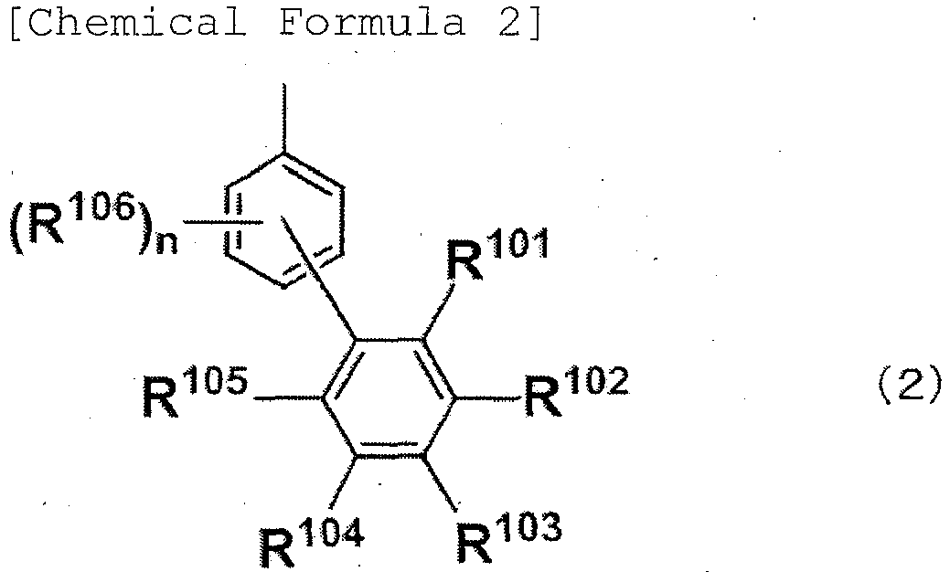
- wherein R101 to R105 may be the same or different, and is hydrogen, a substituted or unsubstituted aryl group, or a ring structure formed between adjacent substituents, with the proviso that at least one of R101 to R105 is a substituted or unsubstituted aryl group, or a ring structure formed between adjacent substituents, and R101 to R105 contain none of an anthracene skeleton and a pyrene skeleton; n R106s are each independently selected from the group consisting of an alkyl group, a cycloalkyl group, an alkoxy group, an alkylthio group and halogen; and n is an integer of 0 to 4:


- wherein R13 to R21 may be the same or different, and are each selected from the group consisting of hydrogen, an alkyl group, a cycloalkyl group, a heterocyclic group, an alkenyl group, a cycloalkenyl group, an alkynyl group, an alkoxy group, an alkylthio group, an aryl ether group, an aryl thioether group, an aryl group, halogen, a carbonyl group, a carboxyl group, an oxycarbonyl group, a carbamoyl group, an amino group, a silyl group and -P(=O)R22R23; and R22 and R23 are each an aryl group or a heteroaryl group, with the proviso that any one of R13 to R21 is coupled at the position of any of R1 to R8 in the general formula (1), R13 to R21 contain none of a dibenzofuran skeleton, a dibenzothiophene skeleton and a carbazole skeleton except that R13 and R21 are coupled at the position of any of R1 to R8 in the general formula (1), and R13 to R23 contain none of an anthracene skeleton and a pyrene skeleton.
- According to the present invention, there can be provided an organic electric field light-emitting device having high luminous efficiency and sufficient durable life.
- The compound represented by the general formula (1) in the present invention is described in detail below.

- wherein R1 to R8 may be the same or different, and are each selected from the group consisting of hydrogen, an alkyl group, a cycloalkyl group, a heterocyclic group, an alkenyl group, a cycloalkenyl group, an alkynyl group, an alkoxy group, an alkylthio group, an aryl ether group, an aryl thioether group, an aryl group, a heteroaryl group, halogen, a carbonyl group, a carboxyl group, an oxycarbonyl group, a carbamoyl group, an amino group, a silyl group and -P(=O)R9R10 and a group represented by the following general formula (3) ; R9 and R10 are each an aryl group or a heteroaryl group, with the proviso that any one of R1 to R8 is a group represented by the following general formula (3), and is coupled at the position of any of R13 to R21 in the general formula (3), R1 to R8 contain none of a dibenzofuran skeleton, a dibenzothiophene skeleton and a carbazole skeleton except that R1 to R8 are each the group represented by the general formula (3), and R1 to R10 contain none of an anthracene skeleton and a pyrene skeleton; A is a group represented by the following general formula (2):

- wherein R101 to R105 may be the same or different, and is hydrogen, a substituted or unsubstituted aryl group, or a ring structure formed between adjacent substituents, with the proviso that at least one of R101 to R105 is a substituted or unsubstituted aryl group, or a ring structure formed between adjacent substituents, and R101 to R105 contain none of an anthracene skeleton and a pyrene skeleton; n R106s are each independently selected from the group consisting of an alkyl group, a cycloalkyl group, an alkoxy group, an alkylthio group and halogen; and n is an integer of 0 to 4:


- wherein R13 to R21 may be the same or different, and are each selected from the group consisting of hydrogen, an alkyl group, a cycloalkyl group, a heterocyclic group, an alkenyl group, a cycloalkenyl group, an alkynyl group, an alkoxy group, an alkylthio group, an aryl ether group, an aryl thioether group, an aryl group, halogen, a carbonyl group, a carboxyl group, an oxycarbonyl group, a carbamoyl group, an amino group, a silyl group and -P(=O)R22R23; and R22 and R23 are each an aryl group or a heteroaryl group, with the proviso that any one of R13 to R21 is coupled at the position of any of R1 to R8 in the general formula (1), R13 to R21 contain none of a dibenzofuran skeleton, a dibenzothiophene skeleton and a carbazole skeleton except that R13 and R21 are coupled at the position of any of R1 to R8 in the general formula (1), and R13 to R23 contain none of an anthracene skeleton and a pyrene skeleton.
- In all of these substituents, hydrogen may be heavy hydrogen. Hydrogen contained in each of the groups described below may be heavy hydrogen.
- The alkyl group denotes a saturated aliphatic hydrocarbon group, such as a methyl group, an ethyl group, a n-propyl group, an isopropyl group, a n-butyl group, a sec-butyl group, or a tert-butyl group, and it may or may not have a substituent. When the alkyl group is substituted, the additional substituent is not particularly limited, examples of the additional substituent may include an alkyl group, an aryl group and a heteroaryl group, and the same holds true in the descriptions below. The number of carbon atoms in the alkyl group is not particularly limited, but from the viewpoints of easy availability and cost, it is normally within the range of 1 or more and 20 or less, more preferably 1 or more and 8 or less.
- The cycloalkyl group denotes a saturated alicyclic hydrocarbon group, such as cyclopropyl, cyclohexyl, norbornyl, or adamantyl, and this may or may not have a substituent. The number of carbon atoms in the alkyl group moiety is not particularly limited, but is normally within the range of 3 or more and 20 or less.
- The heterocyclic group denotes an aliphatic ring having an atom other than carbon in the ring, such as a pyran ring, a piperidine ring, or a cyclic amide, and this may or may not have a substituent. The number of carbon atoms in the heterocyclic group is not particularly limited, but is normally within the range of 2 or more and 20 or less.
- The alkenyl group denotes an unsaturated aliphatic hydrocarbon group containing a double bond, such as a vinyl group, an allyl group, or a butadienyl group, and this may or may not have a substituent. The number of carbon atoms in the alkenyl group moiety is not particularly limited, but is normally within the range of 2 or more and 20 or less.
- The cycloalkenyl group denotes an unsaturated alicyclic hydrocarbon group containing a double bond, such as a cyclopentenyl group, a cyclopentadienyl group, or a cyclohexenyl group, and this may or may not have a substituent. The number of carbon atoms in the cycloalkenyl group is not particularly limited, but is normally within the range of 2 or more and 20 or less.
- The alkynyl group denotes an unsaturated aliphatic hydrocarbon group containing a triple bond, such as an ethynyl group, and this may or may not have a substituent. The number of carbon atoms in the alkynyl group moiety is not particularly limited, but is normally within the range of 2 or more and 20 or less.
- The alkoxy group denotes a functional group with an aliphatic hydrocarbon group bonded via an ether bond, such as a methoxy group, an ethoxy group, or a propoxy group, and this aliphatic hydrocarbon group may or may not have a substituent. The number of carbon atoms in the alkoxy group is not particularly limited, but is normally within the range of 1 or more and 20 or less.
- The alkylthio group is a group in which an oxygen atom of an ether bond in an alkoxy group is substituted with a sulfur atom. The hydrocarbon group of the alkylthio group may or may not have a substituent. The number of carbon atoms in the alkylthio group is not particularly limited, but is normally within the range of 1 or more and 20 or less.
- The aryl ether group denotes a functional group with an aromatic hydrocarbon group bonded via an ether bond, such as a phenoxy group, and the aromatic hydrocarbon group may or may not have a substituent. The number of carbon atoms in the aryl ether group is not particularly limited, but is normally within the range of 6 or more and 40 or less.
- The aryl thioether group is a group in which an oxygen atom of an ether bond in an aryl ether group is substituted with a sulfur atom. The aromatic hydrocarbon group in the aryl ether group may or may not have a substituent. The number of carbon atoms in the aryl ether group is not particularly limited, but is normally within the range of 6 or more and 40 or less.
- The aryl group denotes an aromatic hydrocarbon group, such as a phenyl group, a naphthyl group, a biphenyl group, a fluorenyl group, a phenanthryl group, a triphenylenyl group, or a terphenyl group. The aryl group, may or may not have a substituent. The number of carbon atoms in the aryl group is not particularly limited, but is normally within the range of 6 or more and 40 or less.
- The heteroaryl group denotes a cyclic aromatic group having one or a plurality of atoms other than carbon in the ring, such as a furanyl group, a thiophenyl group, a pyridyl group, a quinolinyl group, a pyrazinyl group, a pyriminidinyl group, a triazinyl group, a naphthyridyl group, a benzofuranyl group, a benzothiophenyl group, or an indolyl group, and this may be unsubstituted or substituted. The number of carbon atoms in the heteroaryl group is not particularly limited, but is normally within the range of 2 or more and 30 or less.
- The halogen denotes fluorine, chlorine, bromine, or iodine.
- The carbonyl group, the carboxyl group, the oxycarbonyl group and the carbamoyl group may or may not have a substituent, and examples of the substituent include an alkyl group, a cycloalkyl group and an aryl group, and these substituents may be further substituted.
- The amino group may or may not have a substituent, and examples of the substituent include an aryl group and a heteroaryl group, and these substituents may be further substituted.
- The silyl group denotes a functional group having a bond with a silicon atom, such as a trimethylsilyl group, and this may or may not have a substituent. The number of carbon atoms in the silyl group is not particularly limited, but is normally within the range of 3 or more and 20 or less. The number of silicon atoms is normally within the range of 1 or more and 6 or less.
- -P(=O)R9R10 and -P(=O)R22R23 may or may not have a substituent, and examples of the substituent include an aryl group and a heteroaryl group, and these substituents may be further substituted.
- The ring structure formed between adjacent substituents means that any two substituents selected from R101 to R105 (e.g., R101 and R102) are bonded to each other to form a conjugated or non-conjugated fused ring when referring to the foregoing general formula (2). This fused ring is a bicyclic fused ring, and may contain one or more of a nitrogen atom, an oxygen atom and a sulfur atom in the structure in the ring.
- Conventional compounds having a carbazole skeleton do not necessarily have sufficient performance as a light-emitting device material. For example, 4,4'-di(9H-carbazol-9-yl)-1,1'-biphenyl (abbreviated name: CBP) and 1,3-di(9H-carbazol-9-yl)benzene (abbreviated name: mCP) are general-purpose materials as a phosphorescence host material and an exciton blocking material, but both have the problem that the driving voltage is high. In studies on improvement of these materials, the present inventors have focused on the hole transporting ability and electron transporting ability of a compound having a carbazole skeleton. Generally, a compound having a carbazole skeleton has a property to transport charges of both a hole and an electron. In contrast, the present inventors have conceived that conventional compounds have a poor hole transporting ability, and therefore the ratio of holes entering an emissive layer is lower than the ratio of electrons entering from an electron transporting layer, so that the balance of charges in the emissive layer is lost, leading to deterioration of device performance, and based on this hypothesis, the present inventors have invented the compound having a carbazole skeleton and represented by the general formula (1).
- The compound represented by the general formula (1) is excellent in hole transporting property as it has a group represented by the general formula (3). The compound having a carbazole skeleton and represented by the general formula (1) can realize a low driving voltage because any one of R13 to R21 in the general formula (3) is used for coupling to R1 to R8 in the general formula (1), i.e., a base skeleton, so that the carbazoles coupled to each other exhibit a high hole transporting property, leading to enhancement of hole mobility in a layer. Since carbazole skeletons are coupled, a high triplet level possessed by the carbazole skeleton itself can be maintained, so that easy deactivation can be suppressed, resulting in achievement of high luminous efficiency. Further, the molecule has an asymmetric structure to increase the effect of suppressing an interaction between carbazole skeletons, so that a stable thin film can be formed, leading to enhancement of durability. Therefore, the above-mentioned compound is preferred.
- Preferably, the compound having a carbazole skeleton and represented by the general formula (1) contains two carbazole skeletons in the molecule, so that the compound has high thin film stability and excellent heat resistance. When three or more carbazole skeletons are contained, thermal decomposition may occur, and therefore it is preferred that two carbazole skeletons are contained.
- Further, R1 to R8 contain none of a dibenzofuran skeleton, a dibenzothiophene skeleton and a carbazole skeleton except that R1 to R8 are each the group represented by the general formula (3). R13 to R21 contain none of a dibenzofuran skeleton, a dibenzothiophene skeleton and a carbazole skeleton except that R13 and R21 are coupled at the position of any of R1 to R8 in the general formula (1). This is because similarly to the above-described reason, when the compound having a carbazole skeleton according to the present invention has as a substituent a carbazole skeleton, or a dibenzofuran skeleton or dibenzothiophene skeleton having a molecular weight comparable to that of the carbazole skeleton, the molecular weight may increase, leading to occurrence of thermal decomposition.
- When the compound having a carbazole skeleton and represented by the general formula (1) has as a substituent on N a biphenyl group having at least one substituted or unsubstituted aryl group (at least one of R101 to R105 is a substituted or unsubstituted aryl group), or a phenyl group having a fused ring group (at least one of R101 to R105 is a ring structure formed between adjacent substituents), the compound shows an excellent electron blocking property. The presence of the aryl group or fused ring group with which the biphenyl group is further substituted increases the glass transition temperature (Tg) of the compound having a carbazole skeleton and represented by the general formula (1), so that the electron blocking property is remarkably enhanced. As a result, the charge balance in the emissive layer can be improved to enhance light-emitting device performance such as luminous efficiency and life. When the number of the aryl groups is 3 or more, synthesis of the compound becomes difficult because of steric complication. Therefore, the number of the aryl groups is preferably 1 or 2.
- The group represented by the general formula (2) is preferably a compound represented by the general formula (4) or (5). That is, the biphenyl group is preferably a meta-biphenyl structure or a para-biphenyl structure from the viewpoint of ease of synthesis.

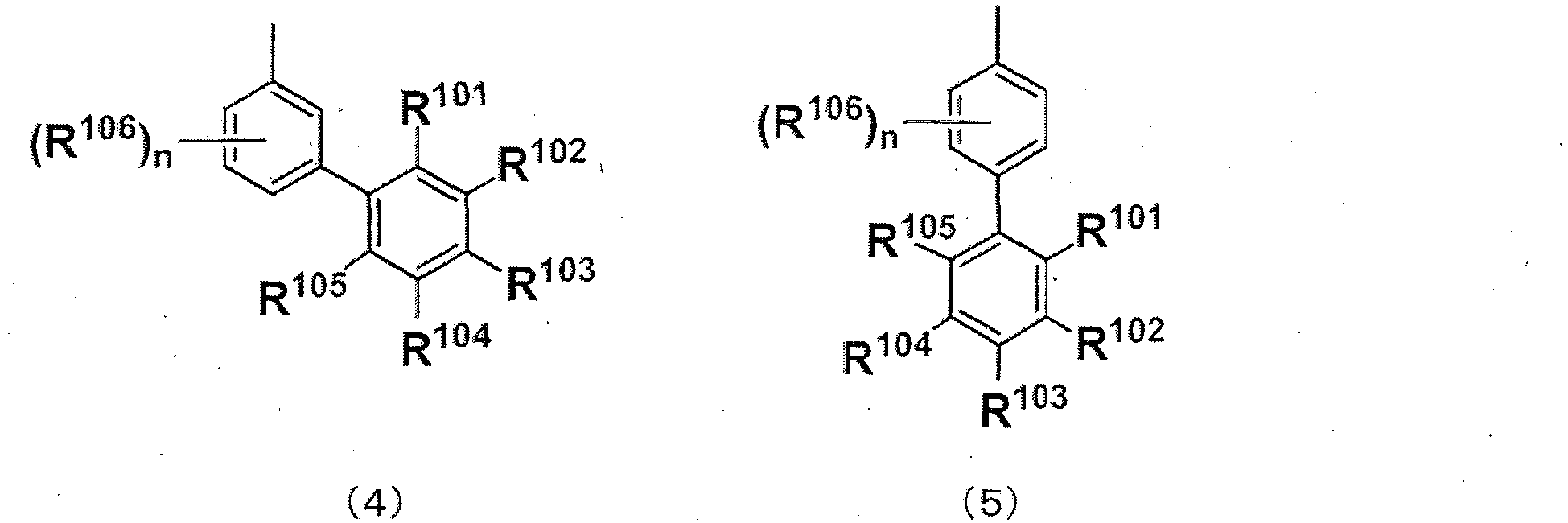
- R101 to R106 and n are as described above. Particularly, at least one of R101 to R105 in the general formula (2) is preferably a substituted or unsubstituted aryl group, and the aryl group is more preferably a phenyl group or a naphthyl group. When the aryl group is substituted, the substituent is preferably one that does not significantly expand the conjugation of the compound or does not lower the triplet level of the compound, and the substituent is more preferably an alkyl group or halogen. When there exist two or more substituted or unsubstituted aryl groups, they may be the same or different.
- R1 to R8 in the general formula (1) and R101 to R105 in the general formula (2) contain none of an anthracene skeleton and a pyrene skeleton. That is, the compound having a carbazole skeleton and represented by the general formula (1) contains none of an anthracene skeleton and a pyrene skeleton in the molecule. This is because the anthracene skeleton and the pyrene skeleton each itself has a low triplet level, and therefore when the compound having a carbazole skeleton according to the present invention has the substituent, the triplet level of the compound is lowered. In the case where the compound having a carbazole skeleton and represented by the general formula (1) is used for the hole transporting layer, luminous efficiency is deteriorated due to occurrence of leakage of triplet excitation energy when the hole transporting layer is in direct contact with an emissive layer containing a triplet emissive dopant if the triplet level is low. In the case where the compound having a carbazole skeleton and represented by the general formula (1) is used for the emissive layer, luminous efficiency is deteriorated because the effect of confining excitation energy by the triplet emissive material cannot be sufficiently exhibited.
- In the compound having a carbazole skeleton and represented by the general formula (1), any one of R1 to R8 is group represented by the general formula (3). In the group represented by the general formula (3), any one of R13 to R21 is used for coupling to R1 to R8. The phrase "R15 is used for coupling to R3" means that the R3 moiety in the general formula (1) and the R15 moiety in the general formula (3) are directly bonded to each other.
- Particularly, it is preferred that R3 is a group represented by the general formula (3) because the hole transporting ability is further enhanced.
- Further, in the compound having a carbazole skeleton and represented by the general formula (1), A and R21 are different groups. In this case, the molecule has an asymmetric structure to increase the effect of suppressing an interaction between carbazole skeletons, so that a more stable thin film can be formed, leading to further enhancement of durability.
- The compound represented by the general formula (1) according to the present invention is preferably a compound in which A is a group represented by any one of the general formulae (6) to (16).


- The substituent (other than the group represented by the general formula (3)) possessed by the compound having a carbazole skeleton and represented by the general formula (1) is preferably hydrogen (including heavy hydrogen), an alkyl group, an aryl group or a heteroaryl group among those described above.
- R21 is preferably an aryl group, more preferably a phenyl group, a naphthyl group or a phenanthryl group. These groups may be further substituted with an alkyl group, halogen, an aryl group or a heteroaryl group, but an anthracenyl group or a pyrenyl group is excluded. When a triplet emissive material is used for the emissive layer, the triplet level of the compound having a carbazole skeleton and represented by the general formula (1) according to the present invention becomes a very important value, and therefore R21 is preferably a substituted or unsubstituted phenyl group having a high triplet level. In this case, the substituent is preferably one that does not significantly expand the conjugation of the compound or does not lower the triplet level of the compound, and the substituent is more preferably an alkyl group or halogen.
- The compound having a carbazole skeleton and represented by the general formula (1) is not particularly limited, and specific examples thereof include the following compounds. The following compounds are illustrative, and compounds other than those specified herein are similarly preferably used as long as they are represented by the general formula (1).


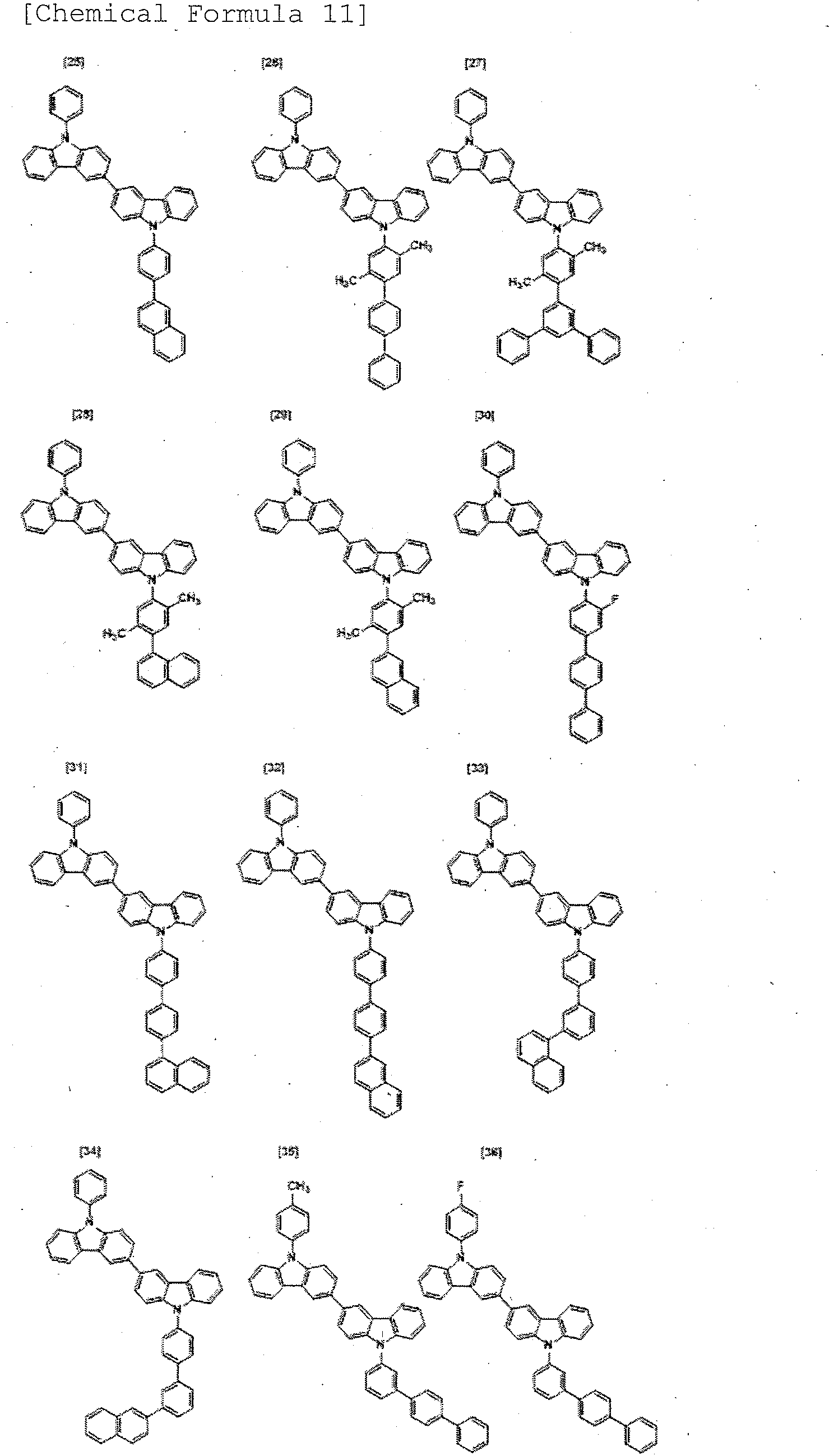


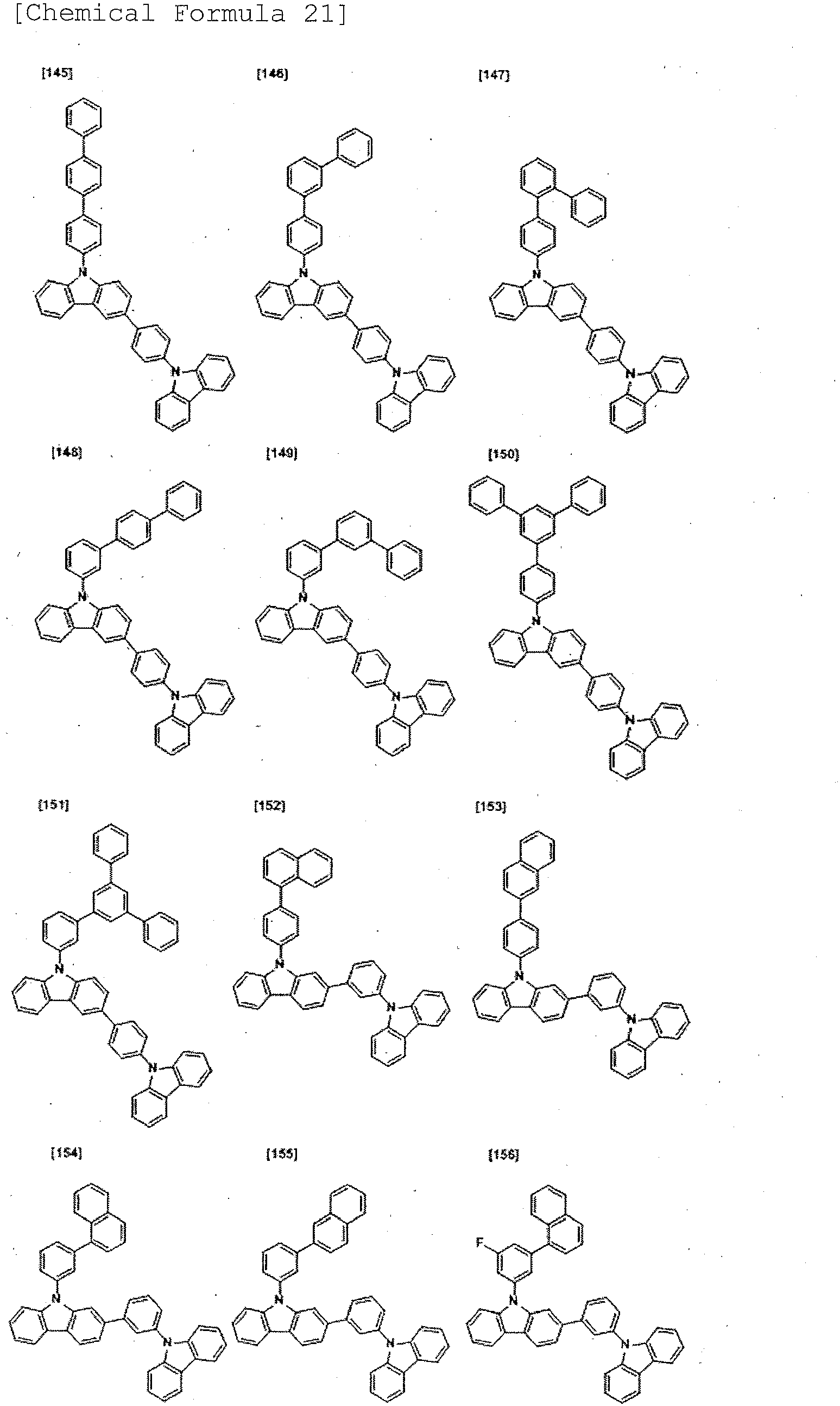


- A known method can be used for synthesis of the compound having a carbazole skeleton as described above. Examples of the method for synthesizing a carbazole dimer include, but are not limited to, a method using a coupling reaction of a carbazole derivative with a halide or a triflate using a palladium or copper catalyst. As one example, an example of using 9-phenylcarbazole-3-boronic acid is shown below.

- In the reaction described above, the reaction similarly proceeds even when a 9-phenylcarbazole-2-boronic acid ester is used in place of 9-phenylcarbazole-3-boronic acid. In this case, a positional isomer of the carbazole dimer can be synthesized.
- Examples of the method for introducing a substituent onto N of carbazole include, but are not limited to, a method using a coupling reaction of a carbazole derivative with a halide using a palladium or copper catalyst.


- The compound represented by the general formula (1) is used as a light-emitting device material. Here, the light-emitting device material in the present invention denotes a material to be used in any layer of a light-emitting device and also includes a material to be used in a protective film of a cathode, in addition to materials to be used in a hole injection layer, a hole transporting layer, an emissive layer and/or an electron transporting layer as described later. Use of the compound represented by the general formula (1) in the present invention in any layer of a light-emitting device can afford high luminous efficiency and also can afford a light-emitting device superior in durability.
- Next, embodiments of the light-emitting device of the present invention will be described in detail. The light-emitting device of the present invention has an anode and a cathode, and an organic layer interposed between the anode and the cathode, and the organic layer emits light by means of electric energy.
- Examples of the layer configuration between the anode and the cathode in such a light-emitting device include, besides a configuration made up of only emissive layer, laminated configurations such as 1) emissive layer/electron transporting layer, 2) hole transporting layer/emissive layer, 3) hole transporting layer/emissive layer/electron transporting layer, 4) hole injection layer/hole transporting layer/emissive layer/electron transporting layer, 5) hole transporting layer/emissive layer/electron transporting layer/electron injection layer, and 6) hole injection layer/hole transporting layer/emissive layer/electron transporting layer/electron injection layer. Each of the layers may be in the form of a single layer or a plurality of layers, and may be doped.
- While the compound represented by the general formula (1) may be used for any layer of the layers described above in a light-emitting device, it is particularly suitably used for the hole transporting layer or the emissive layer.
- In the light-emitting device of the present invention, the anode and the cathode have a role for supplying a sufficient current for light emission of the device, and it is desirable that at least one of them be transparent or translucent in order to take out light. Usually, the anode formed on a substrate is made to be a transparent electrode.
- While the material to be used for an anode is not particularly limited and may be electroconductive metal oxides, such as zinc oxide, tin oxide, indium oxide, tin oxide indium (ITO), and zinc-oxide indium (IZO) ; metals, such as gold, silver, and chromium; inorganic electroconductive substances, such as copper iodide and copper sulfide; or electroconductive polymers, such as polythiophene, polypyrrole, and polyaniline as long as being a material that is capable of injecting holes into an organic layer efficiently and that is transparent or translucent in order to take out light, use of ITO glass or NESA glass is particularly desirable. These electrode materials may be used alone, or a plurality of materials may be used in lamination or in admixture. Since it is favorable that a sufficient current for light emission of the device can be supplied, the resistance of a transparent electrode is not limited, but from the viewpoint of the power consumption of the device, a low resistance is desirable. For example, an ITO substrate having a resistance of 300 Ω/□ or lower functions as a device electrode, but since currently, it is possible to supply a substrate having a resistance of about 10 Ω/□, it is particularly desirable to use a substrate having a low resistance of 20 Ω/□ or lower. The thickness of ITO can be arbitrarily selected according to a resistance value, but ITO is usually used at a thickness of between 50 to 300 nm in many cases.
- In addition, in order to retain the mechanical strength of the light-emitting device, it is preferred to form the light-emitting device on a substrate. As the substrate, a glass substrate such as soda glass or alkali-free glass is suitably used. Since it is favorable that the thickness of a glass substrate has a sufficient thickness for retaining the mechanical strength, a thickness of 0. 5 mm or more is sufficient. Regarding the material of glass, since it is preferred that the amount of ions eluted from glass is small, alkali-free glass is more preferable. Alternatively, since soda lime glass provided with a barrier coating such as SiO2 is commercially available, it can also be used. Further, as far as a first electrode stably functions, it is not necessary that the substrate is glass and, for example, the anode may be formed on a plastic substrate. Examples of a method of forming an ITO film include, but are not particularly limited to, an electron beam method, a sputtering method, and a chemical reaction method.
- A material to be used in the cathode is not particularly limited, as far as it is a substance which can efficiently inject electrons into the emissive layer. Generally, metals such as platinum, gold, silver, copper, iron, tin, aluminum, and indium, or alloys or multilayer lamination of these metals with metals having a low work function such as lithium, sodium, potassium, calcium and magnesium are preferred. Among them, as a main component, aluminum, silver, and magnesium are preferred from the viewpoints of electric resistance value, easiness of making a film, stability of a film, and luminous efficiency. In particular, it is preferred that the material is constituted by magnesium and silver because electron injection into the electron transporting layer and the electron injection layer in the present invention becomes easy, and low voltage driving becomes possible.
- Further, preferable examples include lamination of metals such as platinum, gold, silver, copper, iron, tin, aluminum, and indium, or alloys using these metals, inorganic substances such as silica, titania, and silicon nitride, and organic polymer compounds such as polyvinyl alcohol, polyvinyl chloride, and a hydrocarbon-based polymer compound as a protective film layer on the cathode for protecting the cathode. However, in the case of a device structure for taking out light from the cathode side (top emission structure), the protective film layer is selected from materials having light permeability in a visible light region. Examples of a method for preparation of these electrodes include, but are not particularly limited to, resistance heating, electron beam, sputtering, ion plating and coating.
- The hole injection layer is a layer that is inserted between an anode and a hole transporting layer. The hole injection layer may be in the form of a single layer, or a plurality of layers laminated. It is preferred that the hole injection layer is present between a hole transporting layer and an anode because this successfully results in lower voltage driving, increased durable life, and enhancement in luminous efficiency due to enhancement in the carrier balance of a device.
- The material to be used for the hole injection layer is not particularly limited, and, for example, benzidine derivatives such as 4,4'-bis(N-(3-methylphenyl)-N-phenylamino)biphenyl (TPD), 4,4'-bis(N-(1-naphthyl)-N-phenylamino)biphenyl (NPD), 4,4'-bis(N,N-bis(4-biphenylyl)amino)biphenyl (TBDB), bis(N,N'-diphenyl-4-aminophenyl)-N,N-diphenyl-4,4'-diamino-1,1'-biphenyl (TPD232) and N4,N4'-([1,1'-biphenyl]-4,4'-diyl)bis(N4,N4'N4'-triphenyl-[1 ,1'-biphenyl]-4,4'-diamine); materials called starburst arylamines, such as 4,4',4"-tris(3-methylphenyl(phenyl) amino)triphenylamine (m-MTDATA) and 4,4',4"-tris(1-naphthyl(phenyl)amino)triphenylamine (1-TNATA); biscarbazole derivatives such as bis(N-arylcarbazole) or bis(N-alkylcarbazole); monocarbazole derivatives such as N-([1,1'-biphenyl]-4-yl)-9,9-dimethyl-N-(4-(9-phenyl-9H-car bazol-3-yl)phenyl)-9H-fluorene-2-amine; heterocyclic compounds such as pyrazoline derivatives, stilbene-based compounds, hydrazone-based compounds, benzofuran derivatives, thiophene derivatives, oxadiazole derivatives, phthalocyanine derivatives and porphyrin derivatives; and such polymers as polycarbonates and styrene derivatives having the aforementioned monomers on their side chains, polythiophene, polyaniline, polyfluorene, polyvinylcarbazole and polysilane are used. The compound represented by the general formula (1) can also be used. Among them, benzidine derivatives, starburst arylamine materials and monocarbazole derivatives are more preferably used from the viewpoint of having a lower HOMO level than the compound represented by the general formula (1) and injecting and transporting holes smoothly from an anode to a hole transporting layer.
- These materials may be used alone, or may be used in admixture of two or more thereof. A plurality of materials may be laminated to form a hole injection layer. Further, it is more preferred that the hole injection layer is formed of an acceptor compound alone, or the hole injection material described above is used with the material doped with an acceptor compound used with the above-mentioned hole injection material doped with an acceptor compound because the above-described effects are more remarkably obtained. The acceptor compound is a material that forms a charge transfer complex with an adjacent hole transporting layer when the compound is used as a single-layer film, or forms a charge transfer complex with a material that constitutes a hole injection layer when the compound is used while being doped into the material. Use of such a material enhances the conductivity of a hole injection layer and contributes more to lower the driving voltage of a device, thereby affording effects such as enhancement in luminous efficiency and enhancement in durable life.
- Examples of the acceptor compound include metal chlorides such as iron (III) chloride, aluminum chloride, gallium chloride, indium chloride, and antimony chloride, metal oxides such as molybdenum oxide, vanadium oxide, tungsten oxide, and ruthenium oxide, and charge transfer complexes such as tris(4-bromophenyl)aminium hexachloroantimonate (TBPAH). Moreover, organic compounds having a nitro group, a cyano group, halogen, or a trifluoromethyl group in the molecule, quinone-based compounds, acid anhydride-based compounds, and fullerene can also be used suitably. Specific examples of such compounds include hexacyanobutadiene, hexacyanobenzene, tetracyanoethylene, tetracyanoquinodimethane (TCNQ), tetrafluorotetracyanoquinodimethane (F4-TCNQ), radialene derivatives such as 4,4',4"-((1E,1'E,1"E)-cyclopropane -1,2,3-triylidenetris(cyanomethanylylidene))tris(2,3,5,6-te trafluorobenzonitrile), p-fluoranil, p-chloranil, p-bromanil, p-benzoquinone, 2,6-dichlorobenzoquinone, 2,5-dichlorobenzoquinone, tetramethylbenzoquinone, 1,2,4,5-tetracyanobenzene, o-dicyanobenzene, p-dicyanobenzene, di-pyrazino[2,3-f:2',3'-h]quinoxaline -2,3,6,7,10,11-hexacarbonitrile(HAT(CN)6), 1,4-dicyanotetrafluorobenzene, 2,3-dichloro-5,6-dicyanobenzoquinone, p-dinitrobenzene, m-dinitrobenzene, o-dinitrobenzene, p-cyanonitrobenzene, m-cyanonitrobenzene, o-cyanonitrobenzene, 1,4-naphthoquinone, 2,3-dichloronaphthoquinone, 1-nitronaphthalene, 2-nitronaphthalene, 1,3-dinitronaphthalene, 1,5-dinitronaphthalene, 9-cyanoanthracene, 9-nitroanthracene, 9,10-anthraquinone, 1,3,6,8-tetranitrocarbazole, 2,4,7-trinitro-9-fluorenone, 2,3,5,6-tetracyanopyridine, maleic anhydride, phthalic anhydride, C60, and C70.
- Of these, metal oxides and cyano group-containing compounds are preferred because they can be easily handled and deposited, and therefore the above-described effects can be obtained easily. In either of the case where a hole injection layer is formed of an acceptor compound alone or the case where a hole injection layer is doped with an acceptor compound, the hole injection layer may be a single layer or may be formed of a plurality of layers laminated.
- The hole transporting layer is a layer that transports holes injected from an anode to an emissive layer. The hole transporting layer may be in the form of a single layer, or a plurality of layers laminated.
- The compound represented by the general formula (1) has an ionization potential of 5.3 to 6.0 eV (measured value of deposited film using AC-2 (RIKEN KEIKI Co., Ltd.)), a high triplet level, a high hole transporting property and thin film stability, and is therefore preferably used for the hole injection layer and hole transporting layer of the light-emitting device. The compound represented by the general formula (1) has a larger energy gap as compared to a conventional hole transporting material having a benzidine skeleton, and therefore has a high LUMO level and is excellent in electron blocking property. Further, the compound represented by the general formula (1) is preferably used as a hole transporting material of a device using a triplet emissive material. This is because a conventional hole transporting material having a benzidine skeleton has a low triplet level, so that when the material is in direct contact with an emissive layer containing a triplet emissive dopant, leakage of triplet excitation energy occurs and luminous efficiency is deteriorated, but the compound represented by the general formula (1) has a high triplet level, so that the above-mentioned problem does not occur.
- When the device includes a plurality of hole transporting layers, it is preferred that a hole transporting layer containing the compound represented by the general formula (1) is in direct contact with the emissive layer. This is because the compound represented by the general formula (1) has a high electron blocking property, and therefore can prevent the invasion of electrons flowing out of the emissive layer. Further, the compound represented by the general formula (1) has a high triplet level, and therefore also has an effect of confining the excitation energy of a triplet emissive material. Accordingly, also when the emissive layer contains a triplet emissive material, it is preferred that a hole transporting layer containing the compound represented by the general formula (1) is in direct contact with the emissive layer. Particularly, when an electron transporting host material is used for the emissive layer, excitons generated in the emissive layer are likely leaked to the hole transporting layer side, and therefore the compound of the present invention having a high triplet level is preferably used.
- The hole transporting layer may be formed of only the compound represented by the general formula (1), or other materials may be mixed therein as long as the effects of the present invention are not impaired. In this case, examples of the other materials to be used include benzidine derivatives such as 4,4'-bis(N-(3-methylphenyl)-N-phenylamino)biphenyl (TPD), 4,4'-bis(N-(1-naphthyl)-N-phenylamino)biphenyl (NPD), 4,4'-bis(N,N-bis(4-biphenylyl)amino)biphenyl (TBDB), bis(N,N'-diphenyl-4-aminophenyl)-N,N-diphenyl-4,4'-diamino-1,1'-biphenyl (TPD232) and N4,N4'-( [1,1'-biphenyl]-4,4'-diyl) bis (N4, N4', N4' -triphenyl-[1,1'-biphenyl] -4,4'-diamine); materials called starburst arylamines, such as 4,4',4"-tris (3-methylphenyl(phenyl)amino)triphenylamine (m-MTDATA) and 4,4',4"-tris(1-naphthyl(phenyl)amino)triphenylamine (1-TNATA); biscarbazole derivatives such as bis(N-arylcarbazole) or bis(N-alkylcarbazole); monocarbazole derivatives such as N-([1,1'-biphenyl]-4-yl)-9,9-dimethyl -N-(4-(9-phenyl-9H-carbazol-3-yl)phenyl)-9H-fluorene-2-amin e; heterocyclic compounds such as pyrazoline derivatives, stilbene-based compounds, hydrazone-based compounds, benzofuran derivatives, thiophene derivatives, oxadiazole derivatives, phthalocyanine derivatives and porphyrin derivatives; and such polymers as polycarbonates and styrene derivatives having the aforementioned monomers on their side chains, polythiophene, polyaniline, polyfluorene, polyvinylcarbazole and polysilane.
- The emissive layers may be in the form of a single layer or a plurality of layers, each of which is formed of an emissive material (host material, dopant material), and this may be a mixture of the host material and the dopant material, or the host material alone. That is, in the light-emitting device of the present invention, only the host material or the dopant material may emit light, or both of the host material and the dopant material emit light, in each emissive layer. From the viewpoints that electric energy is efficiently utilized and light emission at high color purity is obtained, it is preferred that the emissive layer includes a mixture of the host material and the dopant material. In addition, the host material and the dopant material may be one kind or a combination of a plurality of kinds, respectively. The dopant material may be contained in a whole host material, or may be partially contained therein. The dopant material may be laminated, or may be dispersed. The dopant material can control an emitted color. When the amount of the dopant material is too large, concentration quenching occurs, and therefore the dopant material is preferably used in an amount of 30% by weight or less, further preferably 20% by weight or less based on the host material. As a doping method, the dopant material can be co-deposited with the host material, or the dopant material, may be mixed with the host material in advance to be deposited simultaneously.
- In addition to the compound represented by the general formula (1), examples of the emissive material that can be used include, but are not particularly limited to, fused ring derivatives such as anthracene and pyrene, metal chelated oxinoid compounds including tris(8-quinolinolato)aluminum, bisstyryl derivatives such as bisstyrylanthracene derivatives and distyrylbenzene derivatives, tetraphenylbutadiene derivatives, indene derivatives, coumarin derivatives, oxadiazole derivatives, pyrrolopyridine derivatives, perinone derivatives, cyclopentadiene derivatives, oxadiazole derivatives, thiadiazolopyridine derivatives, dibenzofuran derivatives, dibenzothiophene derivatives, carbazole derivatives, and indolocarbazole derivatives and, as a polymer series, polyphenylenevinylene derivatives, polyparaphenylene derivatives, and polythiophene derivatives, which have hitherto been known as a light emitting body.
- The host material contained in the emissive material is not needed to be limited to only one kind of compound, and a plurality of compounds of the present invention may be used in admixture, or one or more of other host materials may be used in admixture. Further, these materials may be laminated. The host material is not particularly limited, and examples of the host material which can be used include, but are not particularly limited to, compounds having a fused aryl ring such as naphthalene, anthracene, phenanthrene, pyrene, chrysene, naphthacene, triphenylene, perylene, fluoranthene, fluorene and indene, and derivatives thereof, aromatic amine derivatives such as N,N'-dinaphthyl-N,N'-diphenyl-4,4'-diphenyl -1,1'-diamine, metal chelated oxinoid compounds including tris(8-quinolinato)aluminum (III), bisstyryl derivatives such as distyrylbenzene derivatives, tetraphenylbutadiene derivatives, indene derivatives, coumarin derivatives, oxadiazole derivatives, pyrrolopyridine derivatives, perinone derivatives, cyclopentadiene derivatives, pyrrolopyrrole derivatives, thiadiazolopyridine derivatives, dibenzofuran derivatives, dibenzothiophene derivatives, carbazole derivatives, indolocarbazole derivatives, pyrimidine derivatives and triazine derivatives and, as a polymer series, polyphenylenevinylene derivatives, polyparaphenylene derivatives, polyfluorene derivatives, polyvinylcarbazole derivatives, and polythiophene derivatives. Particularly, as a host to be used when the emissive layer performs triplet emission (phosphorescence emission), metal chelated oxinoid compounds, dibenzofuran derivatives, dibenzothiophene derivatives, carbazole derivatives, indolocarbazole derivatives, pyrimidine derivatives, triazine derivatives, triphenylene derivatives or the like is suitably used.
- Particularly, the compound represented by the general formula (1) has an ionization potential of 5.3 to 6.0 eV (measured value of deposited film using AC-2 (RIKEN KEIKI Co. , Ltd.)), a high triplet level, a high hole transporting property and thin film stability, and is therefore preferably used for the emissive layer of the light-emitting device. The compound represented by the general formula (1) has a larger energy gap as compared to a conventional material having a benzidine skeleton and having a high hole transporting property, and therefore has a high LUMO level and is excellent in electron blocking property. Further, the compound represented by the general formula (1) is preferably used as a host material of a device using a triplet emissive material. This is because the conventional material has a low triplet level, so that when the material is in direct contact with an emissive layer containing a triplet emissive dopant, leakage of triplet excitation energy occurs and luminous efficiency is deteriorated, but the compound represented by the general formula (1) has a high triplet level, so that the above-mentioned problem does not occur. The compound represented by the general formula (1) shows proper hole injection/transporting properties as described above, and also has an improved electron blocking property, and therefore can be used as a hole transporting host. Further, use of the compound in combination with an electron transporting host is preferred because the number of carriers in the emissive layer increases, so that the probability of recombination is increased, resulting in enhancement of luminous efficiency. The electron transporting host material is not particularly limited, but a carbazole compound containing a pyrimidine skeleton or a triazine skeleton, or a compound having a carbazole site is preferably used.
- The dopant material contained in the emissive material is not particularly limited, and examples thereof include compounds having an aryl ring, such as naphthalene, anthracene, phenanthrene, chrysene, fluorene, benzofluorene, pyrene, triphenylene, perylene, fluorene and indene, and derivatives thereof (e.g., 2-(benzothiazol-2-yl)-9,10-diphenylanthracene and 5,6,11,12-tetraphenylnaphthacene); compounds having a heteroaryl ring, such as furan, pyrrole, thiophene, silole, 9-silafluorene, 9,9'-spirobisilafluorene, benzothiophene, benzofuran, indole, dibenzothiophene, dibenzofuran, imidazopyridine, phenanthroline, pyrazine, naphthyridine, quinoxaline, pyrrolopyridine and thioxanthene, and derivatives thereof; distyrylbenzene derivatives; aminostyryl derivatives such as 4,4'-bis(2-(4-diphenylaminophenyl) ethenyl)biphenyl and 4,4'-bis(N-(stilben-4-yl) -N-phenylamino)stilbene; aromatic acetylene derivatives; tetraphenylbutadiene derivatives; stilbene derivatives; aldazine derivatives; pyrromethene derivatives; diketopyrrolo[3,4-c]pyrrole derivatives; coumarin derivatives such as 2,3,5,6-1H,4H-tetrahydro -9-(2'-benzothiazolyl)quinolizino[9,9a,1-gh]coumarin; azole derivatives such as imidazole, thiazole, thiadiazole, carbazole, oxazole, oxadiazole and triazole, and metal complexes thereof; and aromatic amine derivatives represented by N,N'-diphenyl-N,N'-di(3-methylphenyl)-4,4'-diphenyl -1,1'-diamine.
- Particularly, the dopant to be used when the emissive layer performs triplet emission (phosphorescence emission) is preferably a metal complex compound containing at least one metal selected from the group consisting of iridium (Ir), ruthenium (Ru), palladium (Pd), platinum (Pt), osmium (Os), and rhenium (Re). Preferably, a ligand has a nitrogen-containing aromatic heterocyclic ring such as a phenylpyridine skeleton or a phenylquinoline skeleton. However, the complex is not limited thereto, and a suitable complex is selected in connection with an emitted color, device performance and a host compound to be required. Specific examples thereof include tris(2-phenylpyridyl) iridium complexes, tris{2-(2-thiophenyl)pyridyl} iridium complexes, tris{2-(2-benzothiophenyl)pyridyl} iridium complexes, tris(2-phenylbenzothiazole) iridium complexes, tris(2-phenylbenzoxazole) iridium complexes, tris-benzoquinoline iridium complexes, bis(2-phenylpyridyl) (acetylacetonato) iridium complexes, bis{2-(2-thiophenyl) pyridyl} iridium complexes, bis{2-(2-benzothiophenyl) pyridyl}(acetylacetonato) iridium complexes, bis(2-phenylbenzothiazole)(acetylacetonato) iridium complexes, bis(2-phenylbenzoxazole)(acetylacetonato) iridium complexes, bisbenzoquinoline(acetylacetonato) iridium complexes, bis{2-(2,4-difluorophenyl)pyridyl} (acetylacetonato) iridium complexes, tetraethylporphyrin platinum complexes, {tris(thenoyltrifluoroacetone) mono(1,10-phenanthroline)} europium complexes, {tris(thenoyltrifluoroacetone)mono(4,7-diphenyl -1,10-phenanthroline)} europium complexes,{tris(1,3-diphenyl -1,3-propanedione)mono(1,10-phenanthroline)} europium complexes and trisacetylacetone terbium complexes. A phosphorescence dopant described in Japanese Patent Laid-open Publication No.
2009-130141 - Only one of the triplet emissive materials to be used as a dopant material may be contained in an emissive layer, or two or more of the triplet emissive materials may be used in admixture. When two or more triplet emissive materials are used, the total weight of the dopant materials is preferably 30% by weight or less, further preferably 20% by weight or less based on the host material.
- The emissive layer may further contain, in addition to the host material and the triplet emissive material, a third component for adjusting the carrier balance in the emissive layer or for stabilizing the layer structure of the emissive layer. It is to be noted that as the third component, a material is selected which does not cause interaction between a host material made of the compound having a carbazole skeleton and represented by the general formula (1) and a dopant material made of a triplet emissive material.
- Preferable host and dopant in a triplet emission system are not particularly limited, and specific examples thereof include the following.




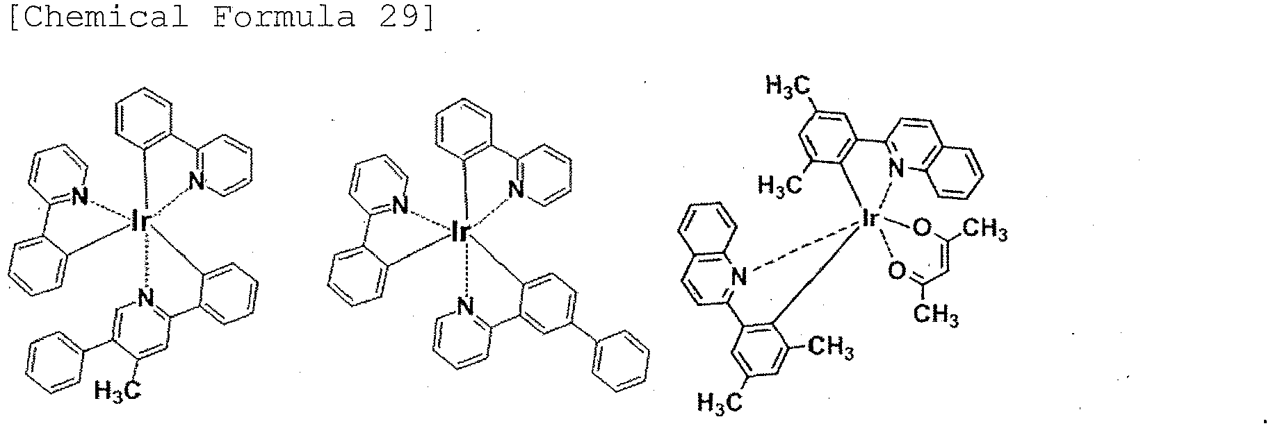
- In addition to the examples described above, hosts and dopants may also be used which are disclosed in Appl. Phys. Lett. 78, 1622 (2001), Nature 395, 151 (1998), Appl. Phys. Lett. 90, 123509 (2007), Org. Electron. 1, 15 (2000),
US Patent Publication No. 2005-202194 ,WO 2005-14551 US Patent publication No. 2003-175553 ,WO 2001-39234 US Patent publication No. 2006-0280965 , Appl. Phys. Lett. 77, 2280 (2000),WO 2004-93207 WO 2005-89025 WO 2006-132173 , Japanese Patent Laid-open No.2005-11610 2007-254297 WO 2007-63796 WO 2007-63754 WO 2008-56746 WO 2008-146839 ,WO 2009-84546 WO 2005-30900 WO 2006-114966 ,US Patent No. 2006-835469 ,US Patent publication No. 2006-202194 ,US Patent publication No. 2007-087321 , Adv. Mater. 19, 739 (2007),WO 2003-40257 US Patent publication No. 2002-034656 ,US Patent publication No. 2006-687266 , Chem. Mater. 16, 2480 (2004),US Patent publication No. 2007-190359 ,US Patent No. 2006-008670 , Japanese Patent Laid-open No.2007-123392 WO 2002-2714 WO 2006-9024 US Patent publication No. 2006-251923 ,WO 2006-56418 US Patent publication No. 2005-260441 ,US Patent publication No. 2007-190359 ,US Patent publication No. 2002-134984 , Angew. Chem. Int. Ed. 47,1 (2008), Chem. Mater. 18, 5119 (2006), Inorg. Chem. 46, 4308 (2007),WO 2005-123873 ,WO 2007-4380 WO 2006-82742 US Patent publication No. 2005-260449 , Organometallics 23, 3745 (2004), Appl. Phys. Lett. 74, 1361 (1999),WO 2006-98120 WO 2006-103874 ,WO 2012-13271 WO 2011-141109 ,WO 2011-55934 WO 2011-139055 ,WO 2011-137072 ,WO 2011-125680 ,WO 2011-132684 ,WO 2011-132683 and the like. - In the present invention, the electron transporting layer is a layer in which electrons are injected from the cathode and, further, which transports the electrons. It is desired that the electron transporting layer has a high electron injection efficiency, and efficiently transports injected electrons. For this reason, the electron transporting layer is required to be constituted by a substance having great electron affinity and, moreover, great electron mobility and, further, excellent stability, and generating impurities that become a trap with difficulty at the time of production and at the time of use. Particularly, when layers are laminated with a large film thickness, a low-molecular weight compound is crystallized or the like to easily degrade film quality, and therefore a compound having a molecular weight of 400 or more, which retains stable film quality, is preferred. However, when transportation balance between holes and electrons is considered, if the electron transporting layer mainly plays a role of being capable of inhibiting holes from the anode from flowing to the cathode side without recombination, even when the layer is constituted by a material having not so high electron transporting ability, the effect of improving luminous efficiency becomes equivalent to that when the layer is constituted by a material having a high electron transporting ability. Therefore, the electron transporting layer in the present invention also includes a hole inhibition layer which can efficiently inhibit the transfer of holes as the same meaning.
- Examples of the electron transporting material to be used for the electron transporting layer include fused polycyclic aromatic derivatives, such as naphthalene and anthracene, styryl-based aromatic derivatives typified by 4,4'-bis(diphenylethenyl)biphenyl, quinone derivatives, such as anthraquinone and diphenoquinone, phosphorus oxide derivatives, and various kinds of metal complexes, such as quinolinol complexes, e.g., tris(8-quinolinolato) aluminum(III), benzoquinolinol complexes, hydroxyazole complexes, azomethine complexes, tropolone metal complexes, and flavonol metal complexes. It is preferred to use a compound that includes an element selected from carbon, hydrogen, nitrogen, oxygen, silicon and phosphorus, and has a heteroaryl ring structure containing electron-accepting nitrogen because it can reduce a driving voltage and a highly efficient light emission can be obtained.
- The electron-accepting nitrogen referred to herein denotes a nitrogen atom which forms a multiple bond with an adjoining atom. Since nitrogen atoms have high electronegativity, the multiple bond has an electron-accepting nature. Therefore, an aromatic heterocyclic ring containing electron-accepting nitrogen has high electron affinity. An electron transporting material having electron-accepting nitrogen makes easier acceptance of electrons from a cathode having higher electron affinity, and lower voltage driving becomes possible. In addition, since supply of electrons to an emissive layer is increased and a recombining probability is increased, luminous efficiency is improved.
- Examples of the heteroaryl ring containing electron-accepting nitrogen include a pyridine ring, a pyrazine ring, a pyrimidine ring, a quinoline ring, a quinoxaline ring, a naphthyridine ring, a pyrimidopyrimidine ring, a benzoquinoline ring, a phenanthroline ring, an imidazole ring, an oxazole ring, an oxadiazole ring, a triazole ring, a thiazole ring, a thiadiazole ring, a benzoxazole ring, a benzothiazole ring, a benzimidazole ring, and a phenanthroimidazole ring.
- Examples of preferred compounds having such a heteroaryl ring structure include benzimidazole derivatives, benzoxazole derivatives, benzothiazole derivatives, oxadiazole derivatives, thiadiazole derivatives, triazole derivatives, pyrazine derivatives, phenanthroline derivatives, quinoxaline derivatives, quinoline derivatives, benzoquinoline derivatives, oligopyridine derivatives such as bipyridine and terpyridine, quinoxaline derivatives and naphthyridine derivatives. Among them, imidazole derivatives such as tris(N-phenylbenzimidazol-2-yl)benzene; oxadiazole derivatives such as 1,3-bis[(4-tert-butylphenyl) 1,3,4-oxadiazolyl]phenylene; triazole derivatives such as N-naphthyl-2,5-diphenyl-1,3,4-triazole; phenanthroline derivatives such as bathocuproine and 1,3-bis(1,10-phenanthrolin-9-yl)benzene; benzoquinoline derivatives such as 2,2'-bis(benzo[h]quinolin-2-yl)-9,9'-spirobifluorene; bipyridine derivatives such as 2,5-bis(6'-(2',2"-bipyridyl)) -1,1-dimethyl-3,4-diphenylsilole; terpyridine derivatives such as 1,3-bis(4'-(2,2':6'2"-terpyridinyl))benzene; and naphthyridine derivatives such as bis(1-naphthyl)-4-(1,8-naphthyridin-2-yl)phenylphosphine oxide are suitably used in view of an electron transporting ability. It is more preferable that such a derivative has a fused polycyclic aromatic skeleton because if so, then the glass transition temperature will increase and an effect of reducing the voltage of a light-emitting device is great due to increased electron mobility. Moreover, considering the improvement in durable life of a device, the easiness of synthesis, and easy availability of raw materials, it is particularly preferable that the fused polycyclic aromatic skeleton is an anthracene skeleton, a pyrene skeleton, or a phenanthroline skeleton. While the electron transporting material may be used alone, two or more kinds of the electron transporting materials may be used in combination, or one or more kinds of other electron transporting materials may be used in combination with the electron transporting material.
- Preferable electron transporting materials are not particularly limited, and specific examples thereof include the following.


- In addition to the examples described above, electron transporting materials may also be used which are disclosed in
WO 2004/63159 WO 2003/60956 WO 2010/113743 andWO 2010/1817 - While the electron transporting material may be used alone, two or more kinds of the electron transporting materials may be used in combination, or one or more kinds of other electron transporting materials may be used in combination with the electron transporting material. Moreover, a donor compound may be contained. The donor compound denotes a compound which makes easy electron injection into the electron transporting layer from the cathode or the electron injection layer and, moreover, enhances the electric conductivity of the electron transporting layer, by improving an electron injection barrier.
- Preferable examples of the donor compound include an alkali metal, an inorganic salt containing an alkali metal, a complex of an alkali metal and an organic substance, an alkaline earth metal, an inorganic salt containing an alkaline earth metal, or a complex of an alkaline earth metal and an organic substance. Examples of the preferable kind of the alkali metal and the alkaline earth metal include alkali metals such as lithium, sodium, potassium, rubidium and cesium, and alkaline earth metals such as magnesium, calcium, cerium and barium which have a low work function and have a great effect of enhancing electron transporting ability.
- In addition, since deposition in vacuum is easy and handling is excellent, the donor compound is preferably in the state of an inorganic salt or a complex with an organic substance rather than a metal single substance. Moreover, from the viewpoints of improvement in easiness in handling in the atmospheric air and easiness in control of the concentration to be added, the donor compound is more preferably in the state of a complex with an organic substance. Examples of the inorganic salt include oxides such as LiO and Li2O, nitrides, fluorides such as LiF, NaF and KF, and carbonates such as Li2CO3, Na2CO3, K2CO3, Rb2CO3 and Cs2CO3. Preferable examples of the alkali metal or alkaline earth metal include lithium and cesium from the viewpoint of obtaining a significant low voltage driving effect. In complexes with an organic substance, preferable examples of the organic substance include quinolinol, benzoquinolinol, pyridylphenol, flavonol, hydroxyimidazopyridine, hydroxybenzazole, and hydroxytriazole. Particularly, a complex of an alkali metal and an organic substance is preferred from the viewpoint of a more significant effect of lowering the voltage of the light-emitting device, and further, a complex of lithium and an organic substance is more preferred from the viewpoint of easiness in synthesis and thermal stability, and lithium quinolinol that can be obtained at a relatively low cost is particularly preferred.
- The ionization potential of the electron transporting layer is not particularly limited, but is preferably 5.6 eV or more and 8.0 eV or less, more preferably 6.0 eV or more and 7.5 eV or less.
- Examples of a method of forming each of the aforementioned layers constituting the light-emitting device include, but are not particularly limited to, resistance heating deposition, electron beam deposition, sputtering, a molecular lamination method, and a coating method, but usually, resistance heating deposition or electron beam deposition is preferable from the viewpoint of device property.
- The thickness of the organic layer depends on the resistance value of an emissive substance and, therefore, it cannot be limited, but it is preferably 1 to 1000 nm. The film thickness of each of the emissive layer, the electron transporting layer and the hole transporting layer is preferably 1 nm or more and 200 nm or less, more preferably 5 nm or more and 100 nm or less.
- The light-emitting device of the present invention has a function of being capable of converting electric energy into light. Herein, a direct current is mainly used as the electric energy, but a pulse current or an alternate current can also be used. A current value and a voltage value are not particularly limited, but when the power consumed and life of the device are considered, they should be selected so that the maximum luminance is obtained by energy as low as possible.
- The light-emitting device of the present invention is used suitably as a display that displays in a matrix and/or segment system.
- In the matrix system, pixels for display are arranged two-dimensionally such as lattice-like arrangement or mosaic-like arrangement, and the collection of pixels displays letters and images. The shape and size of the pixel are determined depending on utility. For example, for displaying images and letters on personal computers, monitors and televisions, a square pixel being 300 µm or less at each side is usually used and, in the case of a large display such as a display panel, a pixel being millimeter order at each side is used. In the case of a monochromatic display, pixels having the same color may be arranged, and in the case of a color display, pixels having red, green and blue colors are arranged to perform display. In this case, typically, there are a delta type and a stripe type. A method of driving this matrix may be either a passive matrix driving method or an active matrix. The passive matrix driving has a simple structure, but when an operation property is considered, the active matrix is more excellent in some cases, and it is necessary to use them properly depending on utility.
- The segment system in the present invention is a system by which a pattern is formed so as to display predetermined information, and a region determined by arrangement of this pattern is made to emit light. Examples thereof include time and temperature displays in digital watches and thermometers, operating-state displays in audio equipment, IH cookers and so on, and panel displays of automobiles. The above-mentioned matrix display and segment display may exist together in the same panel.
- The light-emitting device of the present invention can also be preferably used as backlight of various instruments. Backlight is used mainly for the purpose of enhancing the visibility of display apparatuses which do not emit light by themselves, and is used in liquid crystal display equipment, clocks, audio equipment, automobile panels, display panels, signs, and the like. In particular, the light-emitting device of the present invention is preferably used in backlight for liquid crystal display apparatuses, inter alia, for personal computers which are studied to be thinned, and can provide backlight thinner and lighter than conventional products.
- The present invention will be described by way of Examples, but the present invention is not limited thereto. The number of the compound in each of Examples described below indicates the number of the compound described above.
- A mixed solution of 20.9 g of 3-bromocarbazole, 15.0 g of phenylcarbazole-3-boronic acid, 366 mg of palladium acetate, 300 mg of tris (2-methylphenyl)phosphine, 105 ml of a 2 M aqueous potassium carbonate solution and 260 ml of dimethoxyethane was refluxed for 6 hours under a nitrogen flow. The solution was cooled to room temperature, and then extracted with 500 ml of toluene. The organic layer was washed with 100 ml of water twice, dried over magnesium sulfate, and then evaporated. The resultant concentrate was purified by silica gel column chromatography, and vacuum-dried to obtain 13.5 g of 9-phenyl-9H,9'H-3,3'-bicarbazole.
- Next, a mixed solution of 4.0 g of 4-bromobiphenyl, 3.2 g of 3-chlorophenylboronic acid, 12 mg of bis(triphenylphosphine) palladium(II) dichloride, 21 ml of a 2.0 M aqueous sodium carbonate solution and 40 ml of dimethoxyethane was refluxed for 4 hours under a nitrogen flow. The solution was cooled to room temperature, and then extracted with 100 ml of toluene. The organic layer was washed with 50 ml of water three times, dried over magnesium sulfate, and then evaporated. The resultant concentrate was purified by silica gel column chromatography, and vacuum-dried to obtain 3.7 g of 3-chloro-1,1':4',1"-terphenyl.
- Next, a mixed solution of 2.5 g of 9-phenyl-9H,9'H-3,3'-bicarbazole, 1.9 g of 3-chloro-1,1':4',1"-terphenyl, 35 mg of bis(dibenzylideneacetone) palladium, 43 mg of cBRIDP, 820 mg of sodium tert-butoxide and 30 ml of o-xylene was heated and stirred for 3 hours under reflux under a nitrogen flow. The solution was cooled to room temperature, and then extracted with 100 ml of toluene. The organic layer was washed with 50 ml of water three times, dried over magnesium sulfate, and then evaporated. The resultant concentrate was purified by silica gel column chromatography, and evaporated, and the solid thus obtained was vacuum-dried to obtain 2.8 g of a white solid.
- 1H-NMR analytical results of the resultant powder are as follows, and it was confirmed that the resultant white solid was the compound [1].
1H-NMR (CDCl3 (d=ppm)):7.29-7.82 (m,27H), 7.91 (d,1H), 8.23-8.28 (m,2H), 8.47-8.48 (t,2H) - The compound [1] was used as a light-emitting device material after sublimation purification was performed at about 330°C under a pressure of 1 × 10⁻³ Pa using an oil diffusion pump. The HPLC purity (area % at a measurement wavelength of 254 nm) was 99.8% before sublimation purification, and 99.9% after sublimation purification.
- A mixed solution of 20.9 g of 3-bromocarbazole, 15.0 g of phenylcarbazole-3-boronic acid, 366 mg of palladium acetate, 300 mg of tris (2-methylphenyl)phosphine, 105 ml of a 2 M aqueous potassium carbonate solution and 260 ml of dimethoxyethane was refluxed for 6 hours under a nitrogen flow. The solution was cooled to room temperature, and then extracted with 500 ml of toluene. The organic layer was washed with 100 ml of water twice, dried over magnesium sulfate, and then evaporated. The resultant concentrate was purified by silica gel column chromatography, and vacuum-dried to obtain 13.5 g of 9-phenyl-9H,9'H-3,3'-bicarbazole.
- Next, a mixed solution of 4.0 g of 4-bromochlorobenzene, 5.0 g of 3-biphenylboronic acid, 15 mg of bis(triphenylphosphine) palladium(II) dichloride, 25 ml of a 2.0 M aqueous sodium carbonate solution and 50 ml of dimethoxyethane was refluxed for 4 hours under a nitrogen flow. The solution was cooled to room temperature, and then extracted with 100 ml of toluene. The organic layer was washed with 50 ml of water three times, dried over magnesium sulfate, and then evaporated. The resultant concentrate was purified by silica gel column chromatography, and vacuum-dried to obtain 4.11 g of 4-chloro-1,1':3',1"-terphenyl.
- Next, a mixed solution of 2.5 g of 9-phenyl-9H,9'H-3,3'-bicarbazole, 1.9 g of 4-chloro-1,1':3',1"-terphenyl, 35 mg of bis(dibenzylideneacetone) palladium, 43 mg of cBRIDP, 820 mg of sodium tert-butoxide and 30 ml of o-xylene was heated and stirred for 3 hours under reflux under a nitrogen flow. The solution was cooled to room temperature, and then extracted with 100 ml of toluene. The organic layer was washed with 50 ml of water three times, dried over magnesium sulfate, and then evaporated. The resultant concentrate was purified by silica gel column chromatography, and evaporated, and the solid thus obtained was vacuum-dried to obtain 2.4 g of a white solid.
- 1H-NMR analytical results of the resultant powder are as follows, and it was confirmed that the resultant white solid was the compound [18].
1H-NMR (CDCl3 (d=ppm)):7.29-7.83 (m,25H), 7.89-7.94 (m,3H), 8.24-8.27 (m,2H), 8.47 (d,2H) - The compound [18] was used as a light-emitting device material after sublimation purification was performed at about 330°C under a pressure of 1 × 10⁻³ Pa using an oil diffusion pump. The HPLC purity (area % at a measurement wavelength of 254 nm) was 99.6% before sublimation purification, and 99.9% after sublimation purification.
- A mixed solution of 20.9 g of 3-bromocarbazole, 15.0 g of phenylcarbazole-3-boronic acid, 366 mg of palladium acetate, 300 mg of tris (2-methylphenyl) phosphine, 105 ml of a 2 M aqueous potassium carbonate solution and 260 ml of dimethoxyethane was refluxed for 6 hours under a nitrogen flow. The solution was cooled to room temperature, and then extracted with 500 ml of toluene. The organic layer was washed with 100 ml of water twice, dried over magnesium sulfate, and then evaporated. The resultant concentrate was purified by silica gel column chromatography, and vacuum-dried to obtain 13.5 g of 9-phenyl-9H,9'H-3,3'-bicarbazole.
- Next, a mixed solution of 4.0 g of 4-bromochlorobenzene, 5.0 g of 4-biphenylboronic acid, 15 mg of bis(triphenylphosphine) palladium(II) dichloride, 25 ml of a 2.0 M aqueous sodium carbonate solution and 50 ml of dimethoxyethane was refluxed for 4 hours under a nitrogen flow. The solution was cooled to room temperature, and then extracted with 100 ml of toluene. The organic layer was washed with 50 ml of water three times, dried over magnesium sulfate, and then evaporated. The resultant concentrate was purified by silica gel column chromatography, and vacuum-dried to obtain 4.7 g of 4-chloro-1,1':4',1"-terphenyl.
- Next, a mixed solution of 2.5 g of 9-phenyl-9H,9'H-3,3'-bicarbazole, 1.9 g of 4-chloro-1,1':4',1"-terphenyl, 35 mg of bis(dibenzylideneacetone) palladium, 43 mg of cBRIDP, 820 mg of sodium tert-butoxide and 30 ml of o-xylene was heated and stirred for 3 hours under reflux under a nitrogen flow. The mixture was cooled to room temperature, and then filtered, 100 ml of pure water was added to the resultant solid, and the mixture was stirred for 1 hour, and then filtered. The resultant solid was dissolved in 100 ml of tetrahydrofuran, 300 mg of activated carbon was then added, and the mixture was stirred for 1 hour, filtered, and then evaporated. The resultant solid was vacuum-dried to obtain 1.6 g of a white solid.
- 1H-NMR analytical results of.the resultant powder are as follows, and it was confirmed that the resultant white solid was the compound [19].
1H-NMR (CDCl3 (d=ppm)) :7.30-7.83 (m,26H), 7.89-7.92 (d,2H), 8.24-8.28 (m,2H), 8.47-8.48 (d,2H) - The compound [19] was used as a light-emitting device material after sublimation purification was performed at about 340°C under a pressure of 1 × 10⁻³ Pa using an oil diffusion pump. The HPLC purity (area % at a measurement wavelength of 254 nm) was 99.8% before sublimation purification, and 99.9% after sublimation purification.
- A mixed solution of 20.9 g of 3-bromocarbazole, 15.0 g of 9-phenylcarbazole-3-boronic acid, 366 mg of palladium acetate, 300 mg of tris(2-methylphenyl)phosphine, 105 ml of a 2M aqueous potassium carbonate solution and 260 ml of dimethoxyethane was refluxed for 6 hours under a nitrogen flow. The solution was cooled to room temperature, and then extracted with 500 ml of tetrahydrofuran. The organic layer was washed with 100 ml of a saturated saline solution twice, dried over magnesium sulfate, and then evaporated. The resultant concentrate was purified by o-xylene recrystallization, and vacuum-dried to obtain 13.5 g of 9-phenyl-9H,9'H-3,3'-bicarbazole.
- Next, a mixed solution of 2.9 g of 4-bromochlorobenzene, 5.0 g of 3,5-diphenylbenzeneboronic acid, 11 mg of bis(triphenylphosphine) palladium(II) dichloride, 18 ml of a 2.0 M aqueous sodium carbonate solution and 40 ml of dimethoxyethane was refluxed for 5 hours under a nitrogen flow. The solution was cooled to room temperature, and then extracted with 100 ml of toluene. The organic layer was washed with 50 ml of water three times, dried over magnesium sulfate, and then evaporated. The resultant concentrate was purified by silica gel column chromatography, and vacuum-dried to obtain 3.34 g of 4-chloro-5'-phenyl-1,1':3',1"-terphenyl.
- Next, a mixed solution of 2.5 g of 9-phenyl-9H,9'H-3,3'-bicarbazole, 2.5 g of 4-chloro-5'-phenyl-1,1':3',1"-terphenyl, 35 mg of bis(dibenzylideneacetone) palladium, 43 mg of cBRIDP, 820 mg of sodium tert-butoxide and 30 ml of o-xylene was heated and stirred for 3 hours under reflux under a nitrogen flow. The solution was cooled to room temperature, and then extracted with 100 ml of toluene. The organic layer was washed with 50 ml of water three times, dried over magnesium sulfate, and then evaporated. The resultant concentrate was purified by silica gel column chromatography, and evaporated, and the solid thus obtained was vacuum-dried to obtain 2.4 g of a white solid.
- 1H-NMR analytical results of the resultant powder are as follows, and it was confirmed that the resultant white solid was the compound [21].
1H-NMR (CDCl3 (d=ppm)):7.29-7.68 (m,19H), 7.73-7.99 (m,13H), 8.24-8.28 (m,2H), 8.48 (s,2H)
The compound [21] was used as a light-emitting device material after sublimation purification was performed at about 340°C under a pressure of 1 × 10⁻³ Pa using an oil diffusion pump. The HPLC purity (area % at a measurement wavelength of 254 nm) was 99.7% before sublimation purification, and 99.9% after sublimation purification. - A mixed solution of 20.9 g of 3-bromocarbazole, 15.0 g of phenylcarbazole-3-boronic acid, 366 mg of palladium acetate, 300 mg of tris (2-methylphenyl) phosphine, 105 ml of a 2 M aqueous potassium carbonate solution and 260 ml of dimethoxyethane was refluxed for 6 hours under a nitrogen flow. The solution was cooled to room temperature, and then extracted with 500 ml of toluene. The organic layer was washed with 100 ml of water twice, dried over magnesium sulfate, and then evaporated. The resultant concentrate was purified by silica gel column chromatography, and vacuum-dried to obtain 13.5 g of 9-phenyl-9H,9'H-3,3'-bicarbazole.
- Next, a mixed solution of 4.6 g of 4-bromochlorobenzene, 5.0 g of 1-naphtylboronic acid, 17 mg of bis(triphenylphosphine) palladium(II) dichloride, 29 ml of a 2.0 M aqueous sodium carbonate solution and 60 ml of dimethoxyethane was refluxed for 4 hours under a nitrogen flow. The solution was cooled to room temperature, and then extracted with 150 ml of toluene. The organic layer was washed with 80 ml of water three times, dried over magnesium sulfate, and then evaporated. The resultant concentrate was purified by silica gel column chromatography, and vacuum-dried to obtain 4.5 g of 1-(4-chlorophenyl)naphthalene.
- Next, a mixed solution of 2.5 g of 9-phenyl-9H,9'H-3,3'-bicarbazole, 1.8 g of 1-(4-chlorophenyl)naphthalene, 35 mg of bis(dibenzylideneacetone) palladium, 43 mg of cBRIDP, 820 mg of sodium tert-butoxide and 30 ml of o-xylene was heated and stirred for 3 hours under reflux,under a nitrogen flow. The solution was cooled to room temperature, and then extracted with 100 ml of toluene. The organic layer was washed with 50 ml of water three times, dried over magnesium sulfate, and then evaporated. The resultant concentrate was purified by silica gel column chromatography, and evaporated, and the solid thus obtained was vacuum-dried to obtain 3.1 g of a white solid.
- 1H-NMR analytical results of the resultant powder are as follows, and it was confirmed that the resultant white solid was the compound [24].
1H-NMR (CDCl3 (d=ppm)):7.30-7.69 (m, 17H), 7.78-7.86 (m,6H), 7.92-7.99 (m,2H), 8.06-8.10 (t,1H) 8.24-8.29 (m,2H), 8.48-8.50 (t,2H) - The compound [24] was used as a light-emitting device material after sublimation purification was performed at about 330°C under a pressure of 1 × 10⁻³ Pa using an oil diffusion pump. The HPLC purity (area % at a measurement wavelength of 254 nm) was 99.6% before sublimation purification, and 99.9% after sublimation purification.
- A white solid was obtained by performing synthesis in the same manner as in Synthesis Example 2 except that (3,5-diphenylphenyl)boronic acid was used in place of 3-biphenylboronic acid. 1H-NMR analytical results of the resultant powder are as follows, and it was confirmed that the resultant white solid was the compound [4]. 1H-NMR (DMSO-d6 (d=ppm)):7.29-7.60 (m,20H), 7.65-7.74 (m,7H), 7.80-7.93 (m,10H), 8.02-8.08 (m,4H), 8.22 (s, 1H), 8.39 (t,2H,J=6.8Hz), 8.69 (dd, 2H, 1J=4.3Hz, 2J=1.6Hz).
- The compound [4] was used as a light-emitting device material after sublimation purification was performed at about 350°C under a pressure of 1 × 10⁻³ Pa using an oil diffusion pump. The HPLC purity (area % at a measurement wavelength of 254 nm) was 99.7% before sublimation purification, and 99.9% after sublimation purification.
- A white solid was obtained by performing synthesis in the same manner as in Synthesis Example 2 except that 2-biphenylboronic acid was used in place of 3-biphenylboronic acid. 1H-NMR analytical results of the resultant powder are as follows, and it was confirmed that the resultant white solid was the compound [17].
1H-NMR (DMSO-d6 (d=ppm)):7.20-7.75 (m,26H), 7.88 (dt,2H,1J=8.6Hz,2J=1.8Hz), 8.38(dd,2H,1J=7.7Hz,2J=2.6Hz), 8.68(dd,2H,1J=3.2Hz,2J=1.6Hz). - The compound [17] was used as a light-emitting device material after sublimation purification was performed at about 320°C under a pressure of 1 × 10⁻³ Pa using an oil diffusion pump. The HPLC purity (area % at a measurement wavelength of 254 nm) was 99.7% before sublimation purification, and 99.9% after sublimation purification.
- A white solid was obtained by performing synthesis in the same manner as in Synthesis Example 2 except that 2-naphthaleneboronic acid was-used in place of 3-biphenylboronic acid. 1H-NMR analytical results of the resultant powder are as follows, and it was confirmed that the resultant white solid was the compound [7]. 1H-NMR (DMSO-d6 (d=ppm)) :7.30-7.74 (m,15H), 7.82-8.11 (m,10H), 8.40 (m,3H), 8.70 (dd,2H,1J=4.1Hz,2J=1.6Hz).
- The compound [7] was used as a light-emitting device material after sublimation purification was performed at about 320°C under a pressure of 1 × 10⁻³ Pa using an oil diffusion pump. The HPLC purity (area % at a measurement wavelength of 254 nm) was 99.7% before sublimation purification, and 99.9% after sublimation purification.
- A glass substrate with an ITO transparent electroconductive film deposited thereon in a thickness of 50 nm (manufactured by GEOMATEC Co., Ltd., 11 Ω/□, sputtered product) was cut into 38 × 46 mm, and etched. The resulting substrate was ultrasonically washed with "SEMICOCLEAN 56" (trade name, manufactured by Furuuchi Chemical Corporation) for 15 minutes, and then washed with ultrapure water. This substrate was treated with UV-ozone for 1 hour immediately before preparation of a device, and placed in a vacuum deposition apparatus, and the air was evacuated until the degree of vacuum in the apparatus was 5 × 10⁻⁴ Pa or lower. By a resistance heating method, HI-1 was deposited as a hole injection layer in a thickness of 10 nm. Next, HT-1 was deposited as a first hole transporting layer in a thickness of 110 nm. Next, a compound [1] was deposited as a second hole transporting layer in a thickness of 10 nm. Next, a compound H-1 and a compound D-1 were used as a host material and as a dopant material, respectively, and were deposited as an emissive layer in a thickness of 40 nm so that the doping concentration of the dopant material was 5% by weight. Next, as an electron transporting layer, a compound E-1 was laminated in a thickness of 20 nm.
- Next, lithium fluoride was deposited in a thickness of 0.5 nm, and aluminum was deposited in a thickness of 60 nm to form a cathode, so that a 5 × 5 mm square device was prepared. The film thickness referred to herein is an indicated value on a crystal oscillation film thickness monitor. When the light-emitting device was driven at a direct current of 10 mA/cm2, blue light was emitted with a luminous efficiency of 5.1 lm/W. When the light-emitting device was continuously driven at a direct current of 10 mA/cm2, the luminance decreased by half in 1500 hours. Compounds HI-1, HT-1, H-1, D-1 and E-1 are the compounds shown below.

- Light-emitting devices were prepared in the same manner as in Example 1 except that materials described in Table 1 were used as a second hole transporting layer. The results of the examples are shown in Table 1.
- In the same manner as in Example 1 except that materials described in Table 1 were as a second hole transporting layer, light-emitting devices were prepared and evaluated. The results are shown in Table 1. HT-2 to HT-9 are the compounds shown below.


- A glass substrate with an ITO transparent electroconductive film deposited thereon in a thickness of 50 nm (manufactured by GEOMATEC Co., Ltd., 11 Ω/□, sputtered product) was cut into 38 × 46 mm, and etched. The resulting substrate was ultrasonically washed with "SEMICOCLEAN 56" (trade name, manufactured by Furuuchi Chemical Corporation) for 15 minutes, and then washed with ultrapure water. This substrate was treated with UV-ozone for 1 hour immediately before preparation of a device, and placed in a vacuum deposition apparatus, and the air was evacuated until the degree of vacuum in the apparatus was 5 × 10⁻⁴ Pa or lower. By a resistance heating method, HI-1 was deposited as a hole injection layer in a thickness of 10 nm. Next, HT-1 was deposited as a first hole transporting layer in a thickness of 110 nm. Next, a compound [1] was deposited as a second hole transporting layer in a thickness of 10 nm. Next, a compound H-2 and a compound D-2 were used as a host material and as a dopant material, respectively, and were deposited as an emissive layer in a thickness of 40 nm so that the doping concentration of the dopant material was 10% by weight. Next, a layer obtained by mixing an organic compound (E-2) and a donor compound (lithium quinolinol) at a deposition speed ratio of 1 : 1 (=0.05 nm/s : 0.05 nm/s) was laminated as an electron transporting layer in a thickness of 10 nm.
- Next, lithium quinolinol was deposited in a thickness of 1 nm, and a co-deposited film of magnesium and silver was deposited in a thickness of 100 nm at a deposition speed ratio of magnesium : silver = 10 : 1 (= 0.5 nm/s : 0.05 nm/s) to form a cathode, so that a 5 × 5 mm square device was prepared. The film thickness referred to herein is an indicated value on a crystal oscillation film thickness monitor. When the light-emitting device was driven at a direct current of 10 mA/cm2, green light was emitted with a luminous efficiency of 14.0 lm/W. When the light-emitting device was continuously driven at a direct current of 10 mA/cm2, the luminance decreased by half in 1400 hours. H-2, D-2 and E-2 are the compounds shown below.

- In the same manner as in Example 11 except that materials described in Table 2 were used as a second hole transporting layer, a host material and a dopant material, light-emitting devices were prepared and evaluated. The results are shown in Table 2.
- In the same manner as in Example 11 except that compounds described in Table 2 were used as a second hole transporting layer, a host material and a dopant material, light-emitting devices were prepared and evaluated. The results are shown in Table 2. HT-10 is the compound shown below.

- A glass substrate with an ITO transparent electroconductive film deposited thereon in a thickness of 50 nm (manufactured by GEOMATEC Co., Ltd., 11 Ω/□, sputtered product) was cut into 38 × 46 mm, and etched. The resulting substrate was ultrasonically washed with "SEMICOCLEAN 56" (trade name, manufactured by Furuuchi Chemical Corporation) for 15 minutes, and then washed with ultrapure water. This substrate was treated with UV-ozone for 1 hour immediately before preparation of a device, and placed in a vacuum deposition apparatus, and the air was evacuated until the degree of vacuum in the apparatus was 5 × 10⁻⁴ Pa or lower. By a resistance heating method, HI-1 was deposited as a hole injection layer in a thickness of 10 nm. Next, HT-1 was deposited as a hole transporting layer in a thickness of 125 nm. Next, a compound [1] and a compound D-2 were used as a host material and as a dopant material, respectively, and were deposited as an emissive layer in a thickness of 40 nm so that the doping concentration of the dopant material was 10% by weight. Next, as an electron transporting layer, a compound E-1 was laminated in a thickness of 20 nm.
- Next, lithium fluoride was deposited in a thickness of 0.5 nm, and aluminum was deposited in a thickness of 60 nm to form a cathode, so that a 5 × 5 mm square device was prepared. The film thickness referred to herein is an indicated value on a crystal oscillation film thickness monitor. When the light-emitting device was driven at a direct current of 10 mA/cm2, green light was emitted with a luminous efficiency of 17. 2 lm/W. When the light-emitting device was continuously driven at a direct current of 10 mA/cm2, the luminance decreased by half in 1400 hours.
- In the same manner as in Example 20 except that materials described in Table 3 were used as a hole transporting layer, a host material and a dopant material, light-emitting devices were prepared and evaluated. The results are shown in Table 3.
- In the same manner as in Example 20 except that compounds described in Table 3 were used as a hole transporting layer, a host material and a dopant material, light-emitting devices were prepared and evaluated. The results are shown in Table 3. Compounds H-3, H-4, H-5 and H-6 are the compounds shown below.

- A glass substrate with an ITO transparent electroconductive film deposited thereon in a thickness of 50 nm (manufactured by GEOMATEC Co., Ltd., 11 Ω/□, sputtered product) was cut into 38 × 46 mm, and etched. The resulting substrate was ultrasonically washed with "SEMICOCLEAN 56" (trade name, manufactured by Furuuchi Chemical Corporation) for 15 minutes, and then washed with ultrapure water. This substrate was treated with UV-ozone for 1 hour immediately before preparation of a device, and placed in a vacuum deposition apparatus, and the air was evacuated until the degree of vacuum in the apparatus was 5 × 10⁻⁴ Pa or lower. By a resistance heating method, HI-1 was deposited as a hole injection layer in a thickness of 10 nm. Next, HT-7 was deposited as a first hole transporting layer in a thickness of 90 nm. Next, a compound [1] was deposited as a second hole transporting layer in a thickness of 30 nm. Next, a compound H-7 and a compound D-3 were used as a host material and as a dopant material, respectively, and were deposited as an emissive layer in a thickness of 30 nm so that the doping concentration of the dopant material was 4% by weight. Next, as an electron transporting layer, a compound E-1 was laminated in a thickness of 35 nm.
- Next, lithium fluoride was deposited in a thickness of 0.5 nm, and aluminum was deposited in a thickness of 60 nm to form a cathode, so that a 5 × 5 mm square device was prepared. The film thickness referred to herein is an indicated value on a crystal oscillation film thickness monitor. When the light-emitting device was driven at a direct current of 10 mA/cm2, red light was emitted with a luminous efficiency of 10.5 lm/W. When the light-emitting device was continuously driven at a direct current of 10 mA/cm2, the luminance decreased by half in 1400 hours. Compounds H-7 and D-3 are the compounds shown below.

- In the same manner as, in Example 25 except that materials described in Table 4 were used as a second hole transporting layer, a host material and a dopant material, light-emitting devices were prepared and evaluated. The results are shown in Table 4.
- In the same manner as in Example 25 except that compounds described in Table 4 were used as a second hole transporting layer, a host material and a dopant material, light-emitting devices were prepared and evaluated. The results are shown in Table 4. HT-11 is the compound shown below.
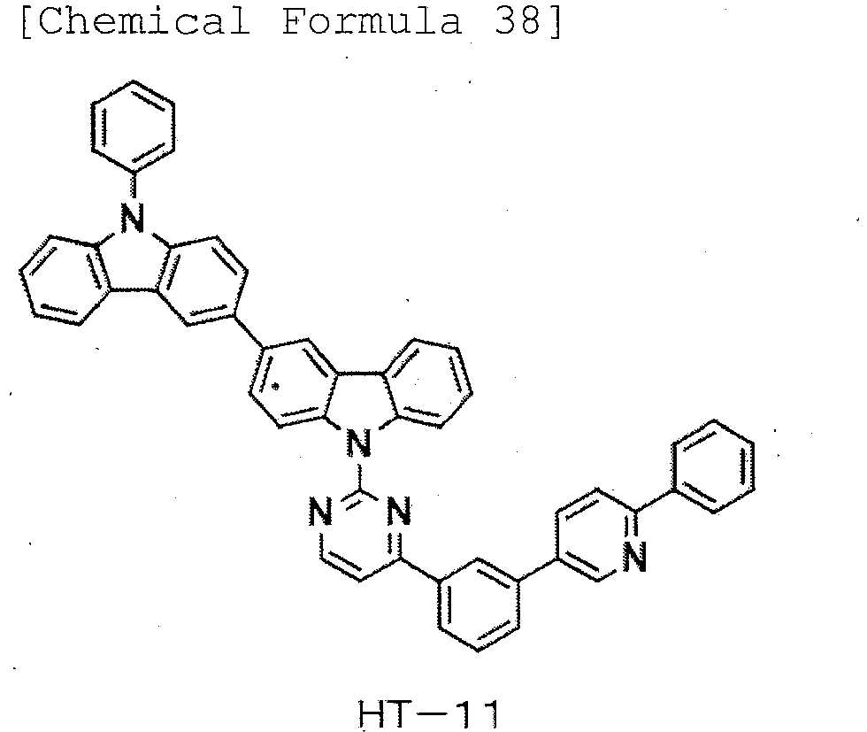
- A glass substrate with an ITO transparent electroconductive film deposited thereon in a thickness of 50 nm (manufactured by GEOMATEC Co., Ltd., 11 Ω/□, sputtered product) was cut into 38 × 46 mm, and etched. The resulting substrate was ultrasonically washed with "SEMICOCLEAN 56" (trade name, manufactured by Furuuchi Chemical Corporation) for 15 minutes, and then washed with ultrapure water. This substrate was treated with UV-ozone for 1 hour immediately before preparation of a device, and placed in a vacuum deposition apparatus, and the air was evacuated until the degree of vacuum in the apparatus was 5 × 10⁻⁴ Pa or lower. By a resistance heating method, HI-1 was deposited as a hole injection layer in a thickness of 10 nm. Next, HT-8 was deposited as a first hole transporting layer in a thickness of 80 nm. Next, a compound [1] was deposited as a second hole transporting layer in a thickness of 10 nm. Next, a compound H-8 and a compound D-4 were used as a host material and as a dopant material, respectively, and were deposited as an emissive layer in a thickness of 30 nm so that the doping concentration of the dopant material was 10% by weight. Next, a layer obtained by mixing an organic compound (E-2) and a donor compound (Liq: lithium quinolinol) at a deposition speed ratio of 1 : 1 (= 0.05 nm/s : 0.05 nm/s) was laminated as an electron transporting layer in a thickness of 35 nm.
- Next, lithium quinolinol was deposited in a thickness of 1 nm, and a co-deposited film of magnesium and silver was deposited in a thickness of 100 nm at a deposition speed ratio of magnesium : silver = 10 : 1 (=0.5 nm/s : 0.05 nm/s) to form a cathode, so that a 5 × 5 mm square device was prepared. The film thickness referred to herein is an indicated value on a crystal oscillation film thickness monitor. When the light-emitting device was driven at a direct current of 10 mA/cm2, green light was emitted with a luminous efficiency of 46.0 lm/W. When the light-emitting device was continuously driven at a direct current of 10 mA/cm2, the luminance decreased by half in 4500 hours. H-8 and D-4 are the compounds shown below.
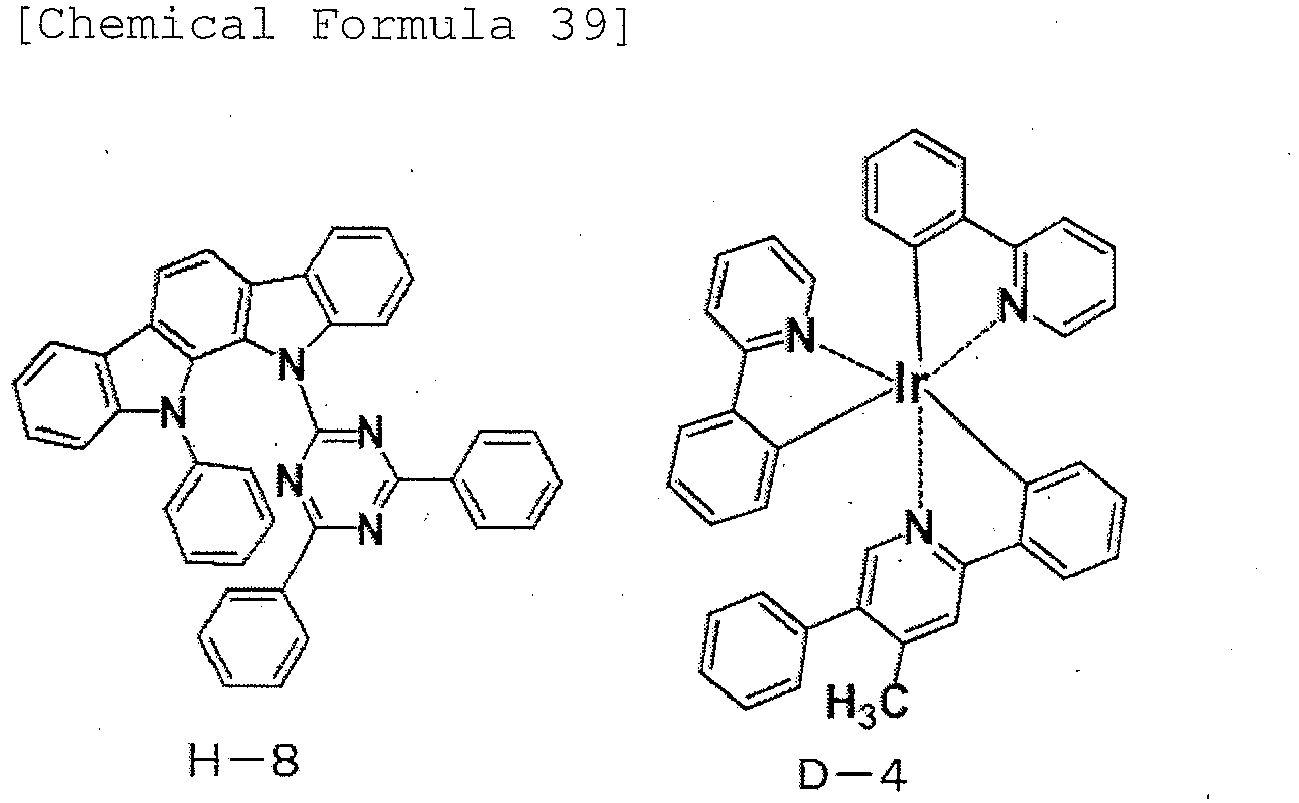
- In the same manner as in Example 33 except that materials described in Table 5 were used as a second hole transporting layer, light-emitting devices were prepared and evaluated. The results are shown in Table 5.
- In the same manner as in Example 33 except that compounds described in Table 5 were used as a second hole transporting layer, light-emitting devices were prepared and evaluated. The results are shown in Table 5. HT-12 is the compound shown below.
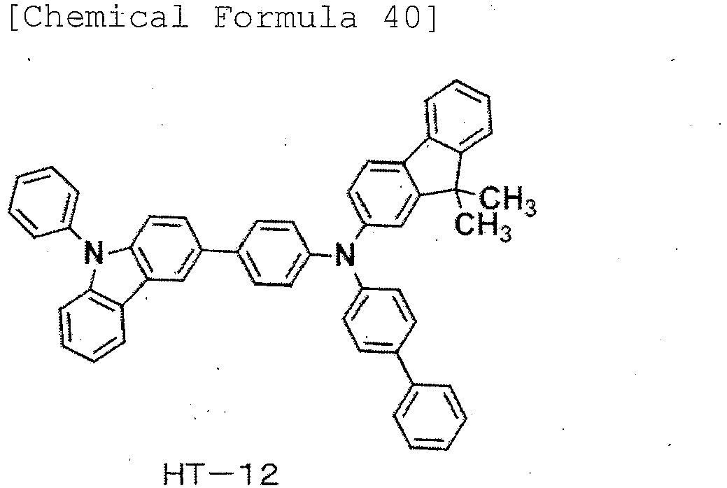
- Light-emitting devices were prepared in the same manner as in Example 33 except that a compound HT-12 and a compound HI-2 were used in place of the compound HI-1, and were deposited as a hole injection layer in a thickness of 10 nm so that the doping concentration of the compound HI-2 was 5% by weight based on the compound HT-12. The results are shown in Table 6. HI-2 is the compound shown below.


- Light-emitting devices were prepared in the same manner as in Examples 40 to 45 except that as a host material, a mixed host of a compound H-8 and a compound H-9 (formed by depositing a co-deposited film of the compound H-8 and the compound H-9 at a deposition speed ratio of 1 : 1, and further depositing a dopant) was used in place of the compound H-8. The results are shown in Table 6. H-9 is the compound shown below.

- Light-emitting devices were prepared in the same manner as in Examples 33 to 39 except that as a hole injection layer, a compound HI-3 was used in place of the compound HI-1. The results are shown in Table 6. HI-3 is the compound shown below.

- Light-emitting devices were prepared in the same manner as in Example 28 except that as an electron transporting layer, materials described in Table 6 were used in place of the layer obtained by mixing a compound E-2 and a donor compound (Liq: lithium quinolinol). The results are shown in Table 6. E-3 to E-7 are the compounds shown below.
- In the same manner as in Example 58 except that compounds described in Table 6 were used as an electron transporting layer, light-emitting devices were prepared and evaluated. The results are shown in Table 6. E-8 and E-9 are the compounds shown below.

- A light-emitting device was prepared in the same manner as in Example 41 except that a compound E-2 and a compound E-1 were laminated in a thickness of 35 nm at a film thickness ratio of 1 : 1 and used as an electron transporting layer in place of the layer obtained by mixing a compound E-2 and a donor compound (Liq: lithium quinolinol). The results are shown in Table 6.
- A light-emitting device was prepared in the same manner as in Example 41 except that a compound E-3 and a compound E-1 were laminated in a thickness of 35 nm at a film thickness ratio of 1 : 1 and used as an electron transporting layer in place of the layer obtained by mixing a compound E-2 and a donor compound (Liq: lithium quinolinol). The results are shown in Table 6.
- A light-emitting device was prepared in the same manner as in Example 41 except that a compound E-4 and a compound E-1 were laminated in a thickness of 35 nm at a film thickness ratio of 1 : 1 and used as an electron transporting layer in place of the layer obtained by mixing a compound E-2 and a donor compound (Liq: lithium quinolinol). The results are shown in Table 6.
[Table 1] Second hole transporting layer Host material Dopant material Emitted color Luminous efficiency (lm/W) Luminance half-value period (h) Example 1 Compound [1] H-1 D-1 Blue 5.1 1500 Example 2 Compound [18] H-1 D-1 Blue 5.3 1600 Example 3 Compound [19] H-1 D-1 Blue 4.8 1400 Example 4 Compound [21] H-1 D-1 Blue 5.3 1500 Example 5 Compound [24] H-1 D-1 Blue 5.1 1500 Example 6 Compound [4] H-1 D-1 Blue 5.3 1700 Example 7 Compound [59] H-1 D-1 Blue 4.5 1300 Example 8 Compound [68] H-1 D-1 Blue 4.6 1300 Example 9 Compound [138] H-1 D-1 Blue 4.4 1250 Example 10 Compound [149] H-1 D-1 Blue 4.5 1300 Comparative Example 1 HT-2 H-1 D-1 Blue 3.5 800 Comparative Example 2 HT-3 H-1 D-1 Blue 3.8 700 Comparative Example 3 HT-4 H-1 D-1 Blue 3.9 700 Comparative Example 4 HT-5 H-1 D-1 Blue 3.6 750 Comparative Example 5 HT-6 H-1 D-1 Blue 3.6 760 Comparative Example 6 HT-7 H-1 D-1 Blue 3.6 800 Comparative Example 7 HT-8 H-1 D-1 Blue 2.1 500 Comparative Example 8 HT-9 H-1 D-1 Blue 2.5 350 [Table 2] Second hole transporting layer Host material Dopant material Emitted color Luminous efficiency (lm/W) Luminance half-value period (h) Example 11 Compound [1] H-2 D-2 Green 14.0 1400 Example 12 Compound [18] H-2 D-2 Green 14.5 1500 Example 13 Compound [19] H-2 D-2 Green 13.5 1300 Example 14 Compound [21] H-2 D-2 Green 15.0 1600 Example 15 Compound [24] H-2 D-2 Green 14.0 1400 Example 16 Compound [17] H-2 D-2 Green 15.0 1600 Example 17 Compound [4] H-2 D-2 Green 15.0 1800 Example 18 Compound [113] H-2 D-2 Green 13.0 1250 Example 19 Compound [173] H-2 D-2 Green 13.0 1300 Comparative Example 9 HT-2 H-2 D-2 Green 9.6 900 Comparative Example 10 HT-3 H-2 D-2 Green 8.5 600 Comparative Example 11 HT-4 H-2 D-2 Green 10.3 700 Comparative Example 12 HT-5 H-2 D-2 Green 7.5 600 Comparative Example 13 HT-6 H-2 D-2 Green 9.4 900 Comparative Example 14 HT-8 H-2 D-2 Green 5.1 300 Comparative Example 15 HT-10 H-2 D-2 Green 5.5 200 [Table 3] Hole transporting layer Host material Dopant material Emitted color Luminous efficiency (lm/W) Luminance half-value period (h) Example 20 HT-1 Compound [1] D-2 Green 17.2 1400 Example 21 HT-1 Compound [18] D-2 Green 18.5 1600 Example 22 HT-1 Compound [21] D-2 Green 19.0 1600 Example 23 HT-1 Compound [88] D-2 Green 16.0 1350 Example 24 HT-1 Compound [170] D-2 Green 16.0 1300 Comparative Example 16 HT-1 H-3 D-2 Green 8.5 550 Comparative Example 17 HT-1 H-4 D-2 Green 9.1 560 Comparative Example 18 HT-1 HT-3 D-2 Green 7.5 700 Comparative Example 19 HT-1 HT-4 D-2 Green 9.5 750 Comparative Example 20 HT-1 HT-6 D-2 Green 8.0 750 Comparative Example 21 HT-1 H-5 D-2 Green 8.5 600 Comparative Example 22 HT-1 H-6 D-2 Green 9.0 700 Comparative Example 23 HT-1 HT-8 D-2 Green 9.5 800 Comparative Example 24 HT-1 HT-10 D-2 Green 9.4 830 [Table 4] Second hole transporting layer Host material Dopant material Emitted color Luminous efficiency (lm/W) Luminance half-value period (h) Example 25 Compound [1] H-7 D-3 Red 10.5 1400 Example 26 Compound [18] H-7 D-3 Red 11.3 1500 Example 27 Compound [19] H-7 D-3 Red 9.8 1300 Example 28 Compound [21] H-7 D-3 Red 11.2 1500 Example 29 Compound [24] H-7 D-3 Red 10.2 1400 Example 30 Compound [4] H-7 D-3 Red 11.0 1500 Example 31 Compound [7] H-7 D-3 Red 11.0 1500 Example 32 Compound [57] H-7 D-3 Red 10.0 1200 Comparative Example 25 HT-2 H-7 D-3 Red 5.6 900 Comparative Example 26 HT-3 H-7 D-3 Red 5.5 800 Comparative Example 27 HT-5 H-7 D-3 Red 5.0 900 Comparative Example 28 HT-7 H-7 D-3 Red 5.4 950 Comparative Example 29 HT-10 H-7 D-3 Red 3.5 600 Comparative Example 30 HT-11 H-7 D-3 Red 3.1 500 [Table 5] Hole injection layer Second hole transporting layer Host material Dopant material Electron transporting layer Emitted color Luminous efficiency (lm/W) Luminance half-value period (h) Example 33 HI-1 Compound [1] H-8 D-4 E-2/Liq Green 46.0 4500 Example 34 HI-1 Compound [18] H-8 D-4 E-2/Liq Green 50.0 5500 Example 35 HI-1 Compound [21] H-8 D-4 E-2/Liq Green 49.0 5500 Example 36 HI-1 Compound [4] H-8 D-4 E-2/Liq Green 53.0 5800 Example 37 HI-1 Compound [6] H-8 D-4 E-2/Liq Green 50.0 5000 Example 38 HI-1 Compound [44] H-8 D-4 E-2/Liq Green 43.0 4000 Example 39 HI-1 Compound [62] H-8 D-4 E-2/Liq Green 41.0 4000 Comparative Example 31 HI-1 HT-3 H-8 D-4 E-2/Liq Green 28.0 2800 Comparative Example 32 HI-1 HT-5 H-8 D-4 E-2/Liq Green 28.0 2700 Comparative Example 33 HI-1 HT-6 H-8 D-4 E-2/Liq Green 29.0 3000 Comparative Example 34 HI-1 HT-7 H-8 D-4 E-2/Liq Green 23.0 2500 Comparative Example 35 HI-1 HT-12 H-8 D-4 E-2/Liq Green 21.0 2500 Comparative Example HI-1 HT-8 H-8 D-4 E-2/Liq Green 19.0 1500 Comparative Example 37 HI-1 HT-11 H-8 D-4 E-2/Liq Green 18.0 1600 [Table 6] Hole injection layer Second hole transporting layer Host material Dopant material Electron transporting layer Emitted color Luminous efficiency (lm/W) Luminance half-value period (h) Example 40 HT-12/HI-2 Compound [1] H-8 D-4 E-2/Liq Green 51.0 5500 Example 41 HT-12/HI-2 Compound [18] H-8 D-4 E-2/Liq Green 55.0 6100 Example 42 HT-12/HI-2 Compound [21] H-8 D-4 E-2/Liq Green 55.0 6000 Example 43 HT-12/HI-2 Compound [4] H-8 D-4 E-2/Liq Green 55.0 6200 Example 44 HT-12/HI-2 Compound [100] H-8 D-4 E-2/Liq Green 41.0 4000 Example 45 HT-12/HI-2 Compound [149] H-8 D-4 E-2/Liq Green 48.0 4800 Example 46 HT-12/HI-2 Compound [1] H-8/H-9 D-4 E-2/Liq Green 41.0 4100 Example 47 HT-12/HI-2 Compound [18] H-8/H-9 D-4 E-2/Liq Green 45.0 4500 Example 48 HT-12/HI-2 Compound [21] H-8/H-9 D-4 E-2/Liq Green 45.0 4400 Example 49 HT-12/HI-2 Compound [4] H-8/H-9 D-4 E-2/Liq Green 45.0 4500 Example 50 HT-12/HI-2 Compound [3] H-8/H-9 D-4 E-2/Liq Green 45.0 4600 Example 51 HT-12/HI-2 Compound [78] H-8/H-9 D-4 E-2/Liq Green 36.0 3500 Example 52 HI-3 Compound [18] H-8 D-4 E-2/Liq Green 38.0 4000 Example 53 HI-3 Compound [18] H-8 D-4 E-2/Liq Green 40.0 4300 Example 54 HI-3 Compound [21] H-8 D-4 E-2/Liq Green 40.0 4200 Example 55 HI-3 Compound [4] H-8 D-4 E-2/Liq Green 42.0 4300 Example 56 HI-3 Compound [90] H-8 D-4 E-2/Liq Green 32.0 3700 Example 57 HI-3 Compound [117] H-8 D-4 E-2/Liq Green 32.0 3700 Example 58 HT-12/HI-2 Compound [18] H-8 D-4 E-3 Green 51.0 5900 Example 59 HT-12/HI-2 Compound [18] H-8 D-4 E-4 Green 50.0 5400 Example 60 HT-12/HI-2 Compound [18] H-8 D-4 E-5 Green 50.0 5800 Example 61 HT-12/HI-2 Compound [18] H-8 D-4 E-6/Liq Green 51.0 6000 Example 62 HT-12/HI-2 Compound [18] H-8 D-4 E-7/Liq Green 48.0 6000 Example 63 HT-12/HI-2 Compound [18] H-8 D-4 E-8 Green 30.0 4000 Example 64 HT-12/HI-2 Compound [18] H-8 D-4 E-9 Green 27.0 3300 Example 65 HT-12/HI-2 Compound [18] H-8 D-4 E-2/E-1 Green 47.0 5700 Example 66 HT-12/HI-2 Compound [18] H-8 D-4 E-3/E-1 Green 44.0 4700 Example 67 HT-12/HI-2 Compound [18] H-8 D-4 E-4/E-1 Green 46.0 5600
Claims (11)
- A light-emitting device material comprising a compound having a carbazole skeleton and represented by the following general formula (1):


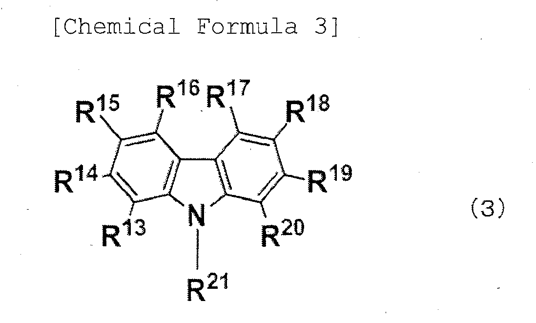
- The light-emitting device material according to claim 1, wherein in the general formula (1), A and R21 are different groups.
- The light-emitting device material according to claim 1 or 2, wherein in the general formula (1), R3 is a group represented by the general formula (3), and is coupled at the position of R15.
- The light-emitting device material according to any one of claims 1 to 3, wherein the group represented by the general formula (2) is a group represented by the following general formula (4) or (5):

- The light-emitting device material according to any one of claims 1 to 4, wherein the group represented by the general formula (2) is a group represented by any of the following general formulae (6) to (16):


- A light-emitting device which has an organic layer between an anode and a cathode and emits light by means of electric energy, wherein the light-emitting device contains the light-emitting device material according to any one of claims 1 to 5 in any of the layers between the anode and the cathode.
- A light-emitting device which has at least a hole transporting layer between an anode and a cathode and emits light by means of electric energy, wherein the light-emitting device contains the light-emitting device material according to any one of claims 1 to 5 in the hole transporting layer.
- A light-emitting device which has at least a hole transporting layer and an emissive layer between an anode and a cathode and emits light by means of electric energy, wherein the light-emitting device contains the light-emitting device material according to any one of claims 1 to 5 in the hole transporting layer, and contains a triplet emissive material in the emissive layer.
- The light-emitting device according to claim 8, wherein the emissive layer has a host material and a triplet emissive dopant material, and the light-emitting device material according to any one of claims 1 to 5 is a host material.
- The light-emitting device according to any one of claims 6 to 9, wherein a hole injection layer exists between the hole transporting layer and the anode, and the hole injection layer contains an acceptor compound.
- The light-emitting device according to any one of claims 6 to 10, wherein at least an electron transporting layer exists between the emissive layer and the cathode, and the electron transporting layer contains a compound containing electron-accepting nitrogen and having a heteroaryl ring structure composed of elements selected from carbon, hydrogen, nitrogen, oxygen, silicon and phosphorus.
Applications Claiming Priority (2)
| Application Number | Priority Date | Filing Date | Title |
|---|---|---|---|
| JP2012164427 | 2012-07-25 | ||
| PCT/JP2013/069910 WO2014017484A1 (en) | 2012-07-25 | 2013-07-23 | Light emitting element material and light emitting element |
Publications (3)
| Publication Number | Publication Date |
|---|---|
| EP2879196A1 true EP2879196A1 (en) | 2015-06-03 |
| EP2879196A4 EP2879196A4 (en) | 2016-02-24 |
| EP2879196B1 EP2879196B1 (en) | 2019-06-19 |
Family
ID=49997293
Family Applications (1)
| Application Number | Title | Priority Date | Filing Date |
|---|---|---|---|
| EP13823334.1A Active EP2879196B1 (en) | 2012-07-25 | 2013-07-23 | Light emitting element material and light emitting element |
Country Status (6)
| Country | Link |
|---|---|
| EP (1) | EP2879196B1 (en) |
| JP (2) | JP6299223B2 (en) |
| KR (1) | KR102095764B1 (en) |
| CN (1) | CN104488105B (en) |
| TW (1) | TWI693212B (en) |
| WO (1) | WO2014017484A1 (en) |
Cited By (9)
| Publication number | Priority date | Publication date | Assignee | Title |
|---|---|---|---|---|
| US20160072075A1 (en) * | 2014-09-05 | 2016-03-10 | Samsung Display Co., Ltd. | Organic light emitting device and display device including the same |
| US10326080B2 (en) | 2014-02-14 | 2019-06-18 | Samsung Display Co., Ltd. | Organic light-emitting devices |
| EP3547385B1 (en) | 2016-11-23 | 2020-11-04 | Guangzhou Chinaray Optoelectronic Materials Ltd. | Organic mixture, composition, and organic electronic component |
| US11456432B2 (en) | 2017-11-01 | 2022-09-27 | Idemitsu Kosan Co., Ltd. | Top emission organic electroluminescent element, organic electroluminescent light emitting device, and electronic device |
| US11974447B2 (en) | 2019-06-14 | 2024-04-30 | Semiconductor Energy Laboratory Co., Ltd. | Light-emitting device, light-emitting apparatus, electronic device, and lighting device |
| US11980094B2 (en) | 2016-11-14 | 2024-05-07 | Universal Display Corporation | Organic electroluminescent materials and devices |
| US12058913B2 (en) | 2019-02-26 | 2024-08-06 | Semiconductor Energy Laboratory Co., Ltd. | Display panel and information processing device |
| US12185558B2 (en) | 2019-02-20 | 2024-12-31 | Semiconductor Energy Laboratory Co., Ltd. | Light-emitting device, light-emitting apparatus, electronic device, and lighting device |
| US12606581B2 (en) | 2020-09-17 | 2026-04-21 | Samsung Display Co., Ltd. | Organometallic compound, organic light-emitting device including the same, and diagnostic composition including the organometallic compound |
Families Citing this family (27)
| Publication number | Priority date | Publication date | Assignee | Title |
|---|---|---|---|---|
| WO2014017484A1 (en) * | 2012-07-25 | 2014-01-30 | 東レ株式会社 | Light emitting element material and light emitting element |
| KR102055684B1 (en) * | 2012-12-27 | 2020-01-23 | 삼성디스플레이 주식회사 | Organic light emitting diode comprising the same |
| TWI540129B (en) * | 2013-11-22 | 2016-07-01 | Dic股份有限公司 | Material for organic electroluminescence device and application thereof, organic electroluminescence device and application thereof |
| WO2015134017A1 (en) * | 2014-03-05 | 2015-09-11 | Universal Display Corporation | Phosphorescent oled devices |
| CN104926805B (en) * | 2014-03-18 | 2019-10-18 | 环球展览公司 | Organic Electroluminescent Materials and Devices |
| US20170170408A1 (en) * | 2014-07-18 | 2017-06-15 | Rohm And Haas Electronic Materials Korea Ltd. | Organic electroluminescent device |
| KR101611213B1 (en) | 2014-09-17 | 2016-04-11 | 주식회사 엘엠에스 | Light-emitting diode and electronic device containing the same |
| US20160111663A1 (en) * | 2014-10-17 | 2016-04-21 | Samsung Display Co., Ltd. | Organic light-emitting device |
| KR102577004B1 (en) * | 2014-10-17 | 2023-09-13 | 삼성디스플레이 주식회사 | Organic light emitting device |
| KR101818579B1 (en) * | 2014-12-09 | 2018-01-15 | 삼성에스디아이 주식회사 | Organic optoelectric device and display device |
| KR101929860B1 (en) | 2015-05-15 | 2018-12-17 | 삼성에스디아이 주식회사 | Organic optoelectronic device and display device |
| KR102059021B1 (en) | 2015-06-19 | 2019-12-24 | 삼성에스디아이 주식회사 | Composition for organic optoelectronic device, organic optoelectric device and display device |
| CN106316925A (en) * | 2015-06-26 | 2017-01-11 | 上海和辉光电有限公司 | Organic electroluminescence compound and application thereof |
| KR102111576B1 (en) | 2015-08-20 | 2020-05-20 | 주식회사 엘엠에스 | Novel compound and light-emitting diode containing the same |
| WO2018168991A1 (en) * | 2017-03-15 | 2018-09-20 | 保土谷化学工業株式会社 | Organic electroluminescent element |
| JP2020143169A (en) * | 2017-05-25 | 2020-09-10 | 出光興産株式会社 | Compositions, materials for organic electroluminescence devices, composition membranes, organic electroluminescence devices, and electronic devices |
| KR101922178B1 (en) * | 2017-11-22 | 2018-11-27 | 삼성디스플레이 주식회사 | Organic light-emitting devices |
| JP2019114780A (en) * | 2017-12-22 | 2019-07-11 | 株式会社半導体エネルギー研究所 | Electronic device, light emitting device, light emitting apparatus, electronic device, and lighting device |
| WO2018101490A2 (en) * | 2018-03-19 | 2018-06-07 | 出光興産株式会社 | Organic electroluminescent element and electronic device |
| EP4174054A1 (en) | 2018-12-28 | 2023-05-03 | Samsung Electronics Co., Ltd. | Heterocyclic compound, composition including the same, and organic light-emitting device including the heterocyclic compound |
| KR102825473B1 (en) | 2019-07-19 | 2025-06-25 | 주식회사 엘지화학 | Polymer, coating composition comprising same, organic light emitting device using same and method of manufacturing same |
| KR102773825B1 (en) | 2019-08-22 | 2025-02-26 | 주식회사 엘지화학 | Polymer, coating compositions comprising same, and organic light emitting device using same |
| US12514115B2 (en) | 2019-10-04 | 2025-12-30 | Idemitsu Kosan Co., Ltd. | Organic electroluminescence device and electronic apparatus |
| WO2021191720A1 (en) * | 2020-03-27 | 2021-09-30 | 株式会社半導体エネルギー研究所 | Light-emitting device composition, light-emitting device, light-emitting apparatus, electronic device, and lighting apparatus |
| CN113896734A (en) | 2020-07-06 | 2022-01-07 | 罗门哈斯电子材料韩国有限公司 | Organic electroluminescent compounds, various host materials and organic electroluminescent device comprising the same |
| KR102931207B1 (en) | 2020-08-28 | 2026-02-25 | 주식회사 엘지화학 | Polymer, coating composition comprising same, organic light emitting device using same and method of manufacturing same |
| US20240224800A1 (en) | 2021-06-18 | 2024-07-04 | Nippon Steel Chemical & Material Co., Ltd. | Material for organic electroluminescent elements, and organic electroluminescent element |
Citations (2)
| Publication number | Priority date | Publication date | Assignee | Title |
|---|---|---|---|---|
| JPH11214154A (en) | 1997-10-15 | 1999-08-06 | Toray Ind Inc | Manufacturing method of organic electroluminescent device |
| JP2003133075A (en) | 2001-07-25 | 2003-05-09 | Toray Ind Inc | Light emitting element |
Family Cites Families (75)
| Publication number | Priority date | Publication date | Assignee | Title |
|---|---|---|---|---|
| JP3139321B2 (en) * | 1994-03-31 | 2001-02-26 | 東レ株式会社 | Light emitting element |
| US6830828B2 (en) | 1998-09-14 | 2004-12-14 | The Trustees Of Princeton University | Organometallic complexes as phosphorescent emitters in organic LEDs |
| US6458475B1 (en) | 1999-11-24 | 2002-10-01 | The Trustee Of Princeton University | Organic light emitting diode having a blue phosphorescent molecule as an emitter |
| US20020121638A1 (en) | 2000-06-30 | 2002-09-05 | Vladimir Grushin | Electroluminescent iridium compounds with fluorinated phenylpyridines, phenylpyrimidines, and phenylquinolines and devices made with such compounds |
| JP3812730B2 (en) | 2001-02-01 | 2006-08-23 | 富士写真フイルム株式会社 | Transition metal complex and light emitting device |
| US7166368B2 (en) | 2001-11-07 | 2007-01-23 | E. I. Du Pont De Nemours And Company | Electroluminescent platinum compounds and devices made with such compounds |
| US6863997B2 (en) | 2001-12-28 | 2005-03-08 | The Trustees Of Princeton University | White light emitting OLEDs from combined monomer and aggregate emission |
| KR100691543B1 (en) | 2002-01-18 | 2007-03-09 | 주식회사 엘지화학 | New material for electron transport and organic light emitting device using the same |
| EP1582516B1 (en) | 2003-01-10 | 2013-07-17 | Idemitsu Kosan Co., Ltd. | Nitrogenous heterocyclic derivative and organic electroluminescent element employing the same |
| EP1595933A4 (en) * | 2003-02-20 | 2009-04-08 | Idemitsu Kosan Co | MATERIAL FOR ORGANIC ELECTROLUMINESCENT DEVICES, AND ORGANIC ELECTROLUMINESCENCE DEVICE COMPRISING SUCH MATERIAL |
| EP1618170A2 (en) | 2003-04-15 | 2006-01-25 | Covion Organic Semiconductors GmbH | Mixtures of matrix materials and organic semiconductors capable of emission, use of the same and electronic components containing said mixtures |
| JP2005011610A (en) | 2003-06-18 | 2005-01-13 | Nippon Steel Chem Co Ltd | Organic electroluminescence device |
| TWI390006B (en) | 2003-08-07 | 2013-03-21 | Nippon Steel Chemical Co | Organic EL materials with aluminum clamps |
| HU0302888D0 (en) | 2003-09-09 | 2003-11-28 | Pribenszky Csaba Dr | In creasing of efficacity of stable storage by freezing of embryos in preimplantation stage with pretreatment by pressure |
| US20060269780A1 (en) | 2003-09-25 | 2006-11-30 | Takayuki Fukumatsu | Organic electroluminescent device |
| US7607634B2 (en) | 2004-03-12 | 2009-10-27 | Gm Global Technology Operations, Inc. | Shape memory polymer conduits and methods of use |
| TW200531592A (en) | 2004-03-15 | 2005-09-16 | Nippon Steel Chemical Co | Organic electroluminescent device |
| US7491823B2 (en) | 2004-05-18 | 2009-02-17 | The University Of Southern California | Luminescent compounds with carbene ligands |
| US7279704B2 (en) | 2004-05-18 | 2007-10-09 | The University Of Southern California | Complexes with tridentate ligands |
| WO2005123873A1 (en) | 2004-06-17 | 2005-12-29 | Konica Minolta Holdings, Inc. | Organic electroluminescent device material, organic electroluminescent device, display and illuminating device |
| US20060008670A1 (en) | 2004-07-06 | 2006-01-12 | Chun Lin | Organic light emitting materials and devices |
| EP2271183B1 (en) | 2004-07-23 | 2015-03-18 | Konica Minolta Holdings, Inc. | Organic electroluminescent element, display and illuminator |
| WO2006025186A1 (en) * | 2004-09-01 | 2006-03-09 | Hirose Engineering Co., Ltd. | Dicarbazyl compound, process for producing the same, dicarbazyl polymer, and luminescent element |
| DE102004057072A1 (en) | 2004-11-25 | 2006-06-01 | Basf Ag | Use of Transition Metal Carbene Complexes in Organic Light Emitting Diodes (OLEDs) |
| GB2437453B (en) | 2005-02-04 | 2011-05-04 | Konica Minolta Holdings Inc | Material for organic electroluminescence element, organic electroluminescence element, display device and lighting device |
| JP2006241077A (en) | 2005-03-03 | 2006-09-14 | Idemitsu Kosan Co Ltd | Luminescent metal complex, method for producing the same, and organic electroluminescent light emitting device using the same |
| KR100803125B1 (en) | 2005-03-08 | 2008-02-14 | 엘지전자 주식회사 | Red phosphorescent compound and organic light emitting device using the same |
| JP5125502B2 (en) | 2005-03-16 | 2013-01-23 | コニカミノルタホールディングス株式会社 | Organic electroluminescence element material, organic electroluminescence element |
| JPWO2006103874A1 (en) | 2005-03-29 | 2008-09-04 | コニカミノルタホールディングス株式会社 | ORGANIC ELECTROLUMINESCENT ELEMENT MATERIAL, ORGANIC ELECTROLUMINESCENT ELEMENT, DISPLAY DEVICE AND LIGHTING DEVICE |
| WO2006114966A1 (en) | 2005-04-18 | 2006-11-02 | Konica Minolta Holdings, Inc. | Organic electroluminescent device, display and illuminating device |
| US9051344B2 (en) | 2005-05-06 | 2015-06-09 | Universal Display Corporation | Stability OLED materials and devices |
| WO2006130598A2 (en) | 2005-05-31 | 2006-12-07 | Universal Display Corporation | Triphenylene hosts in phosphorescent light emitting diodes |
| CN101193875B (en) | 2005-06-07 | 2011-05-11 | 新日铁化学株式会社 | Organic metal complex and organic electroluminescent device using same |
| WO2007004380A1 (en) | 2005-07-01 | 2007-01-11 | Konica Minolta Holdings, Inc. | Organic electroluminescent element material, organic electroluminescent element, display device, and lighting equipment |
| JP4887731B2 (en) | 2005-10-26 | 2012-02-29 | コニカミノルタホールディングス株式会社 | Organic electroluminescence element, display device and lighting device |
| JPWO2007063796A1 (en) | 2005-12-01 | 2009-05-07 | 新日鐵化学株式会社 | Organic electroluminescence device |
| WO2007063754A1 (en) | 2005-12-01 | 2007-06-07 | Nippon Steel Chemical Co., Ltd. | Compound for organic electroluminescent element and organic electroluminescent element |
| BRPI0707552B8 (en) | 2006-02-10 | 2020-05-05 | Universal Display Corp | metal complexes of imidazo [1,2-f] phenanthridine and diimized [1,2-a: 1 ', 2'-c] quinazoline cyclometallated and isoelectronic and benzanulated analogs thereof and oled devices that encompass them |
| JP4823730B2 (en) | 2006-03-20 | 2011-11-24 | 新日鐵化学株式会社 | Luminescent layer compound and organic electroluminescent device |
| US8062769B2 (en) | 2006-11-09 | 2011-11-22 | Nippon Steel Chemical Co., Ltd. | Indolocarbazole compound for use in organic electroluminescent device and organic electroluminescent device |
| KR100863905B1 (en) * | 2007-01-15 | 2008-10-17 | 삼성에스디아이 주식회사 | Fluorine-containing compound and organic light emitting device using same |
| TWI468489B (en) | 2007-05-29 | 2015-01-11 | Nippon Steel & Sumikin Chem Co | Organic electroluminescent element compounds and organic electroluminescent elements |
| JP2009130141A (en) | 2007-11-22 | 2009-06-11 | Idemitsu Kosan Co Ltd | Organic EL device and organic EL material-containing solution |
| WO2009084546A1 (en) | 2007-12-27 | 2009-07-09 | Nippon Steel Chemical Co., Ltd. | Compound for organic electroluminescent device and organic electroluminescent device using the same |
| KR101668887B1 (en) | 2008-07-01 | 2016-10-24 | 도레이 카부시키가이샤 | Light-emitting element |
| KR20100079458A (en) | 2008-12-31 | 2010-07-08 | 덕산하이메탈(주) | Bis-carbazole compound and organic electric element using same, terminal thereof |
| WO2010095621A1 (en) * | 2009-02-18 | 2010-08-26 | 出光興産株式会社 | Aromatic amine derivative and organic electroluminescent element |
| JP5012998B2 (en) | 2009-03-30 | 2012-08-29 | 東レ株式会社 | Light emitting device material and light emitting device |
| US8962158B2 (en) * | 2009-03-31 | 2015-02-24 | Nippon Steel & Sumikin Chemical Co., Ltd. | Material having indolocarbazole compound for phosphorescent light-emitting element and organic electroluminescent element using the same |
| KR101506999B1 (en) | 2009-11-03 | 2015-03-31 | 제일모직 주식회사 | Compound for organic photoelectric device and organic photoelectric device including the same |
| JP5584702B2 (en) * | 2009-12-28 | 2014-09-03 | 新日鉄住金化学株式会社 | Organic electroluminescence device |
| KR101419666B1 (en) | 2010-03-31 | 2014-07-15 | 이데미쓰 고산 가부시키가이샤 | Material for organic electroluminescence element, and organic electroluminescence element using same |
| EP2415769B1 (en) | 2010-04-20 | 2015-10-28 | Idemitsu Kosan Co., Ltd. | Bis-carbazole derivative, material for organic electroluminescent element and organic electroluminescent element using same |
| US8227801B2 (en) | 2010-04-26 | 2012-07-24 | Universal Display Corporation | Bicarbzole containing compounds for OLEDs |
| KR20110122051A (en) | 2010-05-03 | 2011-11-09 | 제일모직주식회사 | Compound for organic photoelectric device and organic photoelectric device comprising same |
| DE102010020044A1 (en) | 2010-05-11 | 2011-11-17 | Merck Patent Gmbh | Organic electroluminescent device |
| EP2595208A1 (en) * | 2010-07-13 | 2013-05-22 | Toray Industries, Inc. | Light emitting element |
| JP5968885B2 (en) | 2010-07-30 | 2016-08-10 | メルク パテント ゲーエムベーハー | Organic electroluminescence device |
| KR20120020901A (en) * | 2010-08-31 | 2012-03-08 | 롬엔드하스전자재료코리아유한회사 | Novel compounds for organic electronic material and organic electroluminescent device using the same |
| US8932734B2 (en) * | 2010-10-08 | 2015-01-13 | Universal Display Corporation | Organic electroluminescent materials and devices |
| US9450192B2 (en) * | 2010-12-06 | 2016-09-20 | E-Ray Optoelectronics Technology | Carbazole derivative and organic electroluminescent devices utilizing the same and fabrication method thereof |
| KR101478000B1 (en) | 2010-12-21 | 2015-01-05 | 롬엔드하스전자재료코리아유한회사 | Novel organic electroluminescent compounds and organic electroluminescent device using the same |
| KR20140000684A (en) * | 2010-12-27 | 2014-01-03 | 도레이 카부시키가이샤 | Light emitting element material and light emitting element |
| TWI538977B (en) * | 2011-02-07 | 2016-06-21 | Idemitsu Kosan Co | A double carbazole derivative and an organic electroluminescent element using the same |
| JP5964328B2 (en) * | 2011-02-11 | 2016-08-03 | ユニバーサル ディスプレイ コーポレイション | ORGANIC LIGHT EMITTING DEVICE AND MATERIAL FOR USE IN THE ORGANIC LIGHT EMITTING DEVICE |
| KR101427611B1 (en) * | 2011-03-08 | 2014-08-11 | 롬엔드하스전자재료코리아유한회사 | Novel compounds for organic electronic material and organic electroluminescence device using the same |
| KR20120116269A (en) * | 2011-04-12 | 2012-10-22 | 롬엔드하스전자재료코리아유한회사 | Novel compounds for organic electronic material and organic electroluminescence device using the same |
| KR101443756B1 (en) * | 2011-05-26 | 2014-09-23 | 제일모직 주식회사 | Compound for organic OPTOELECTRONIC device, ORGANIC LIGHT EMITTING DIODE INCLUDING THE SAME and DISPLAY INCLUDING THE organic LIGHT EMITTING DIODE |
| KR20130025087A (en) * | 2011-09-01 | 2013-03-11 | 롬엔드하스전자재료코리아유한회사 | Novel organic electroluminescent compounds and organic electroluminescent device using the same |
| US20140217393A1 (en) * | 2011-09-09 | 2014-08-07 | Idemitsu Kosan Co., Ltd. | Organic electroluminescence element |
| KR20140094520A (en) * | 2011-10-26 | 2014-07-30 | 이데미쓰 고산 가부시키가이샤 | Organic electroluminescence element, and material for organic electroluminescence element |
| KR20130062583A (en) * | 2011-12-05 | 2013-06-13 | 롬엔드하스전자재료코리아유한회사 | Novel organic electroluminescence compounds and organic electroluminescence device using the same |
| KR102009697B1 (en) * | 2012-03-05 | 2019-10-23 | 도레이 카부시키가이샤 | Light emitting element |
| WO2013187894A1 (en) * | 2012-06-14 | 2013-12-19 | Universal Display Corporation | Biscarbazole derivative host materials and red emitter for oled emissive region |
| WO2014017484A1 (en) * | 2012-07-25 | 2014-01-30 | 東レ株式会社 | Light emitting element material and light emitting element |
-
2013
- 2013-07-23 WO PCT/JP2013/069910 patent/WO2014017484A1/en not_active Ceased
- 2013-07-23 CN CN201380038765.8A patent/CN104488105B/en active Active
- 2013-07-23 JP JP2013540120A patent/JP6299223B2/en active Active
- 2013-07-23 KR KR1020147036851A patent/KR102095764B1/en active Active
- 2013-07-23 EP EP13823334.1A patent/EP2879196B1/en active Active
- 2013-07-24 TW TW102126504A patent/TWI693212B/en active
-
2017
- 2017-11-21 JP JP2017223414A patent/JP6658719B2/en active Active
Patent Citations (2)
| Publication number | Priority date | Publication date | Assignee | Title |
|---|---|---|---|---|
| JPH11214154A (en) | 1997-10-15 | 1999-08-06 | Toray Ind Inc | Manufacturing method of organic electroluminescent device |
| JP2003133075A (en) | 2001-07-25 | 2003-05-09 | Toray Ind Inc | Light emitting element |
Non-Patent Citations (1)
| Title |
|---|
| See also references of WO2014017484A1 |
Cited By (12)
| Publication number | Priority date | Publication date | Assignee | Title |
|---|---|---|---|---|
| US10326080B2 (en) | 2014-02-14 | 2019-06-18 | Samsung Display Co., Ltd. | Organic light-emitting devices |
| US10333077B2 (en) | 2014-02-14 | 2019-06-25 | Samsung Display Co., Ltd. | Organic light-emitting devices |
| US20160072075A1 (en) * | 2014-09-05 | 2016-03-10 | Samsung Display Co., Ltd. | Organic light emitting device and display device including the same |
| US9876178B2 (en) * | 2014-09-05 | 2018-01-23 | Samsung Display Co., Ltd. | Organic light emitting device and display device including the same |
| US11980094B2 (en) | 2016-11-14 | 2024-05-07 | Universal Display Corporation | Organic electroluminescent materials and devices |
| EP3547385B1 (en) | 2016-11-23 | 2020-11-04 | Guangzhou Chinaray Optoelectronic Materials Ltd. | Organic mixture, composition, and organic electronic component |
| US11456432B2 (en) | 2017-11-01 | 2022-09-27 | Idemitsu Kosan Co., Ltd. | Top emission organic electroluminescent element, organic electroluminescent light emitting device, and electronic device |
| US12185558B2 (en) | 2019-02-20 | 2024-12-31 | Semiconductor Energy Laboratory Co., Ltd. | Light-emitting device, light-emitting apparatus, electronic device, and lighting device |
| US12058913B2 (en) | 2019-02-26 | 2024-08-06 | Semiconductor Energy Laboratory Co., Ltd. | Display panel and information processing device |
| US11974447B2 (en) | 2019-06-14 | 2024-04-30 | Semiconductor Energy Laboratory Co., Ltd. | Light-emitting device, light-emitting apparatus, electronic device, and lighting device |
| US12302685B2 (en) | 2019-06-14 | 2025-05-13 | Semiconductor Energy Laboratory Co., Ltd. | Light-emitting device, light-emitting apparatus, electronic device, and lighting device |
| US12606581B2 (en) | 2020-09-17 | 2026-04-21 | Samsung Display Co., Ltd. | Organometallic compound, organic light-emitting device including the same, and diagnostic composition including the organometallic compound |
Also Published As
| Publication number | Publication date |
|---|---|
| TWI693212B (en) | 2020-05-11 |
| KR102095764B1 (en) | 2020-04-02 |
| TW201412712A (en) | 2014-04-01 |
| JP6299223B2 (en) | 2018-03-28 |
| KR20150039131A (en) | 2015-04-09 |
| JP2018061052A (en) | 2018-04-12 |
| EP2879196A4 (en) | 2016-02-24 |
| EP2879196B1 (en) | 2019-06-19 |
| CN104488105B (en) | 2017-03-22 |
| CN104488105A (en) | 2015-04-01 |
| WO2014017484A1 (en) | 2014-01-30 |
| JP6658719B2 (en) | 2020-03-04 |
| JPWO2014017484A1 (en) | 2016-07-11 |
Similar Documents
| Publication | Publication Date | Title |
|---|---|---|
| EP2879196B1 (en) | Light emitting element material and light emitting element | |
| EP2709181B1 (en) | Light-emitting element material and light-emitting element | |
| EP2816626B1 (en) | Light-emitting element material, and light-emitting element | |
| EP2688120B1 (en) | Light-emitting element material and light-emitting element | |
| JP6183211B2 (en) | Light emitting device material and light emitting device | |
| JPWO2013133219A1 (en) | Light emitting element | |
| EP2626920A1 (en) | Light emitting element material and light emitting element | |
| WO2016009823A1 (en) | Monoamine derivative, luminescent element material comprising same, and luminescent element | |
| WO2018180709A1 (en) | Compound, electronic device containing same, organic thin film light emitting element, display device and lighting device |
Legal Events
| Date | Code | Title | Description |
|---|---|---|---|
| PUAI | Public reference made under article 153(3) epc to a published international application that has entered the european phase |
Free format text: ORIGINAL CODE: 0009012 |
|
| 17P | Request for examination filed |
Effective date: 20150112 |
|
| AK | Designated contracting states |
Kind code of ref document: A1 Designated state(s): AL AT BE BG CH CY CZ DE DK EE ES FI FR GB GR HR HU IE IS IT LI LT LU LV MC MK MT NL NO PL PT RO RS SE SI SK SM TR |
|
| AX | Request for extension of the european patent |
Extension state: BA ME |
|
| DAX | Request for extension of the european patent (deleted) | ||
| REG | Reference to a national code |
Ref country code: DE Ref legal event code: R079 Ref document number: 602013056890 Country of ref document: DE Free format text: PREVIOUS MAIN CLASS: H01L0051500000 Ipc: H01L0051540000 |
|
| RA4 | Supplementary search report drawn up and despatched (corrected) |
Effective date: 20160121 |
|
| RIC1 | Information provided on ipc code assigned before grant |
Ipc: H01L 51/54 20060101AFI20160115BHEP Ipc: C09K 11/06 20060101ALI20160115BHEP Ipc: C07D 209/86 20060101ALI20160115BHEP |
|
| TPAC | Observations filed by third parties |
Free format text: ORIGINAL CODE: EPIDOSNTIPA |
|
| STAA | Information on the status of an ep patent application or granted ep patent |
Free format text: STATUS: EXAMINATION IS IN PROGRESS |
|
| 17Q | First examination report despatched |
Effective date: 20171124 |
|
| GRAP | Despatch of communication of intention to grant a patent |
Free format text: ORIGINAL CODE: EPIDOSNIGR1 |
|
| STAA | Information on the status of an ep patent application or granted ep patent |
Free format text: STATUS: GRANT OF PATENT IS INTENDED |
|
| INTG | Intention to grant announced |
Effective date: 20190215 |
|
| GRAS | Grant fee paid |
Free format text: ORIGINAL CODE: EPIDOSNIGR3 |
|
| GRAA | (expected) grant |
Free format text: ORIGINAL CODE: 0009210 |
|
| STAA | Information on the status of an ep patent application or granted ep patent |
Free format text: STATUS: THE PATENT HAS BEEN GRANTED |
|
| AK | Designated contracting states |
Kind code of ref document: B1 Designated state(s): AL AT BE BG CH CY CZ DE DK EE ES FI FR GB GR HR HU IE IS IT LI LT LU LV MC MK MT NL NO PL PT RO RS SE SI SK SM TR |
|
| REG | Reference to a national code |
Ref country code: GB Ref legal event code: FG4D |
|
| REG | Reference to a national code |
Ref country code: CH Ref legal event code: EP |
|
| REG | Reference to a national code |
Ref country code: IE Ref legal event code: FG4D |
|
| REG | Reference to a national code |
Ref country code: DE Ref legal event code: R096 Ref document number: 602013056890 Country of ref document: DE |
|
| REG | Reference to a national code |
Ref country code: AT Ref legal event code: REF Ref document number: 1146634 Country of ref document: AT Kind code of ref document: T Effective date: 20190715 |
|
| REG | Reference to a national code |
Ref country code: NL Ref legal event code: MP Effective date: 20190619 |
|
| PG25 | Lapsed in a contracting state [announced via postgrant information from national office to epo] |
Ref country code: NO Free format text: LAPSE BECAUSE OF FAILURE TO SUBMIT A TRANSLATION OF THE DESCRIPTION OR TO PAY THE FEE WITHIN THE PRESCRIBED TIME-LIMIT Effective date: 20190919 Ref country code: HR Free format text: LAPSE BECAUSE OF FAILURE TO SUBMIT A TRANSLATION OF THE DESCRIPTION OR TO PAY THE FEE WITHIN THE PRESCRIBED TIME-LIMIT Effective date: 20190619 Ref country code: LT Free format text: LAPSE BECAUSE OF FAILURE TO SUBMIT A TRANSLATION OF THE DESCRIPTION OR TO PAY THE FEE WITHIN THE PRESCRIBED TIME-LIMIT Effective date: 20190619 Ref country code: AL Free format text: LAPSE BECAUSE OF FAILURE TO SUBMIT A TRANSLATION OF THE DESCRIPTION OR TO PAY THE FEE WITHIN THE PRESCRIBED TIME-LIMIT Effective date: 20190619 Ref country code: SE Free format text: LAPSE BECAUSE OF FAILURE TO SUBMIT A TRANSLATION OF THE DESCRIPTION OR TO PAY THE FEE WITHIN THE PRESCRIBED TIME-LIMIT Effective date: 20190619 Ref country code: FI Free format text: LAPSE BECAUSE OF FAILURE TO SUBMIT A TRANSLATION OF THE DESCRIPTION OR TO PAY THE FEE WITHIN THE PRESCRIBED TIME-LIMIT Effective date: 20190619 |
|
| REG | Reference to a national code |
Ref country code: LT Ref legal event code: MG4D |
|
| PG25 | Lapsed in a contracting state [announced via postgrant information from national office to epo] |
Ref country code: GR Free format text: LAPSE BECAUSE OF FAILURE TO SUBMIT A TRANSLATION OF THE DESCRIPTION OR TO PAY THE FEE WITHIN THE PRESCRIBED TIME-LIMIT Effective date: 20190920 Ref country code: LV Free format text: LAPSE BECAUSE OF FAILURE TO SUBMIT A TRANSLATION OF THE DESCRIPTION OR TO PAY THE FEE WITHIN THE PRESCRIBED TIME-LIMIT Effective date: 20190619 Ref country code: RS Free format text: LAPSE BECAUSE OF FAILURE TO SUBMIT A TRANSLATION OF THE DESCRIPTION OR TO PAY THE FEE WITHIN THE PRESCRIBED TIME-LIMIT Effective date: 20190619 Ref country code: BG Free format text: LAPSE BECAUSE OF FAILURE TO SUBMIT A TRANSLATION OF THE DESCRIPTION OR TO PAY THE FEE WITHIN THE PRESCRIBED TIME-LIMIT Effective date: 20190919 |
|
| REG | Reference to a national code |
Ref country code: AT Ref legal event code: MK05 Ref document number: 1146634 Country of ref document: AT Kind code of ref document: T Effective date: 20190619 |
|
| PG25 | Lapsed in a contracting state [announced via postgrant information from national office to epo] |
Ref country code: RO Free format text: LAPSE BECAUSE OF FAILURE TO SUBMIT A TRANSLATION OF THE DESCRIPTION OR TO PAY THE FEE WITHIN THE PRESCRIBED TIME-LIMIT Effective date: 20190619 Ref country code: SK Free format text: LAPSE BECAUSE OF FAILURE TO SUBMIT A TRANSLATION OF THE DESCRIPTION OR TO PAY THE FEE WITHIN THE PRESCRIBED TIME-LIMIT Effective date: 20190619 Ref country code: CZ Free format text: LAPSE BECAUSE OF FAILURE TO SUBMIT A TRANSLATION OF THE DESCRIPTION OR TO PAY THE FEE WITHIN THE PRESCRIBED TIME-LIMIT Effective date: 20190619 Ref country code: NL Free format text: LAPSE BECAUSE OF FAILURE TO SUBMIT A TRANSLATION OF THE DESCRIPTION OR TO PAY THE FEE WITHIN THE PRESCRIBED TIME-LIMIT Effective date: 20190619 Ref country code: EE Free format text: LAPSE BECAUSE OF FAILURE TO SUBMIT A TRANSLATION OF THE DESCRIPTION OR TO PAY THE FEE WITHIN THE PRESCRIBED TIME-LIMIT Effective date: 20190619 Ref country code: PT Free format text: LAPSE BECAUSE OF FAILURE TO SUBMIT A TRANSLATION OF THE DESCRIPTION OR TO PAY THE FEE WITHIN THE PRESCRIBED TIME-LIMIT Effective date: 20191021 Ref country code: AT Free format text: LAPSE BECAUSE OF FAILURE TO SUBMIT A TRANSLATION OF THE DESCRIPTION OR TO PAY THE FEE WITHIN THE PRESCRIBED TIME-LIMIT Effective date: 20190619 |
|
| PG25 | Lapsed in a contracting state [announced via postgrant information from national office to epo] |
Ref country code: IT Free format text: LAPSE BECAUSE OF FAILURE TO SUBMIT A TRANSLATION OF THE DESCRIPTION OR TO PAY THE FEE WITHIN THE PRESCRIBED TIME-LIMIT Effective date: 20190619 Ref country code: ES Free format text: LAPSE BECAUSE OF FAILURE TO SUBMIT A TRANSLATION OF THE DESCRIPTION OR TO PAY THE FEE WITHIN THE PRESCRIBED TIME-LIMIT Effective date: 20190619 Ref country code: SM Free format text: LAPSE BECAUSE OF FAILURE TO SUBMIT A TRANSLATION OF THE DESCRIPTION OR TO PAY THE FEE WITHIN THE PRESCRIBED TIME-LIMIT Effective date: 20190619 Ref country code: IS Free format text: LAPSE BECAUSE OF FAILURE TO SUBMIT A TRANSLATION OF THE DESCRIPTION OR TO PAY THE FEE WITHIN THE PRESCRIBED TIME-LIMIT Effective date: 20191019 |
|
| REG | Reference to a national code |
Ref country code: CH Ref legal event code: PL |
|
| PG25 | Lapsed in a contracting state [announced via postgrant information from national office to epo] |
Ref country code: TR Free format text: LAPSE BECAUSE OF FAILURE TO SUBMIT A TRANSLATION OF THE DESCRIPTION OR TO PAY THE FEE WITHIN THE PRESCRIBED TIME-LIMIT Effective date: 20190619 Ref country code: MC Free format text: LAPSE BECAUSE OF FAILURE TO SUBMIT A TRANSLATION OF THE DESCRIPTION OR TO PAY THE FEE WITHIN THE PRESCRIBED TIME-LIMIT Effective date: 20190619 |
|
| REG | Reference to a national code |
Ref country code: BE Ref legal event code: MM Effective date: 20190731 |
|
| PG25 | Lapsed in a contracting state [announced via postgrant information from national office to epo] |
Ref country code: PL Free format text: LAPSE BECAUSE OF FAILURE TO SUBMIT A TRANSLATION OF THE DESCRIPTION OR TO PAY THE FEE WITHIN THE PRESCRIBED TIME-LIMIT Effective date: 20190619 Ref country code: DK Free format text: LAPSE BECAUSE OF FAILURE TO SUBMIT A TRANSLATION OF THE DESCRIPTION OR TO PAY THE FEE WITHIN THE PRESCRIBED TIME-LIMIT Effective date: 20190619 |
|
| PG25 | Lapsed in a contracting state [announced via postgrant information from national office to epo] |
Ref country code: CH Free format text: LAPSE BECAUSE OF NON-PAYMENT OF DUE FEES Effective date: 20190731 Ref country code: IS Free format text: LAPSE BECAUSE OF FAILURE TO SUBMIT A TRANSLATION OF THE DESCRIPTION OR TO PAY THE FEE WITHIN THE PRESCRIBED TIME-LIMIT Effective date: 20200224 Ref country code: BE Free format text: LAPSE BECAUSE OF NON-PAYMENT OF DUE FEES Effective date: 20190731 Ref country code: LU Free format text: LAPSE BECAUSE OF NON-PAYMENT OF DUE FEES Effective date: 20190723 Ref country code: LI Free format text: LAPSE BECAUSE OF NON-PAYMENT OF DUE FEES Effective date: 20190731 |
|
| REG | Reference to a national code |
Ref country code: DE Ref legal event code: R097 Ref document number: 602013056890 Country of ref document: DE |
|
| PLBE | No opposition filed within time limit |
Free format text: ORIGINAL CODE: 0009261 |
|
| STAA | Information on the status of an ep patent application or granted ep patent |
Free format text: STATUS: NO OPPOSITION FILED WITHIN TIME LIMIT |
|
| PG2D | Information on lapse in contracting state deleted |
Ref country code: IS |
|
| PG25 | Lapsed in a contracting state [announced via postgrant information from national office to epo] |
Ref country code: IE Free format text: LAPSE BECAUSE OF NON-PAYMENT OF DUE FEES Effective date: 20190723 Ref country code: FR Free format text: LAPSE BECAUSE OF NON-PAYMENT OF DUE FEES Effective date: 20190819 |
|
| 26N | No opposition filed |
Effective date: 20200603 |
|
| PG25 | Lapsed in a contracting state [announced via postgrant information from national office to epo] |
Ref country code: SI Free format text: LAPSE BECAUSE OF FAILURE TO SUBMIT A TRANSLATION OF THE DESCRIPTION OR TO PAY THE FEE WITHIN THE PRESCRIBED TIME-LIMIT Effective date: 20190619 |
|
| GBPC | Gb: european patent ceased through non-payment of renewal fee |
Effective date: 20190919 |
|
| PG25 | Lapsed in a contracting state [announced via postgrant information from national office to epo] |
Ref country code: GB Free format text: LAPSE BECAUSE OF NON-PAYMENT OF DUE FEES Effective date: 20190919 |
|
| PG25 | Lapsed in a contracting state [announced via postgrant information from national office to epo] |
Ref country code: CY Free format text: LAPSE BECAUSE OF FAILURE TO SUBMIT A TRANSLATION OF THE DESCRIPTION OR TO PAY THE FEE WITHIN THE PRESCRIBED TIME-LIMIT Effective date: 20190619 |
|
| PG25 | Lapsed in a contracting state [announced via postgrant information from national office to epo] |
Ref country code: HU Free format text: LAPSE BECAUSE OF FAILURE TO SUBMIT A TRANSLATION OF THE DESCRIPTION OR TO PAY THE FEE WITHIN THE PRESCRIBED TIME-LIMIT; INVALID AB INITIO Effective date: 20130723 Ref country code: MT Free format text: LAPSE BECAUSE OF FAILURE TO SUBMIT A TRANSLATION OF THE DESCRIPTION OR TO PAY THE FEE WITHIN THE PRESCRIBED TIME-LIMIT Effective date: 20190619 |
|
| PG25 | Lapsed in a contracting state [announced via postgrant information from national office to epo] |
Ref country code: MK Free format text: LAPSE BECAUSE OF FAILURE TO SUBMIT A TRANSLATION OF THE DESCRIPTION OR TO PAY THE FEE WITHIN THE PRESCRIBED TIME-LIMIT Effective date: 20190619 |
|
| REG | Reference to a national code |
Ref country code: DE Ref legal event code: R079 Ref document number: 602013056890 Country of ref document: DE Free format text: PREVIOUS MAIN CLASS: H01L0051540000 Ipc: H10K0085000000 |
|
| P01 | Opt-out of the competence of the unified patent court (upc) registered |
Effective date: 20230515 |
|
| PGFP | Annual fee paid to national office [announced via postgrant information from national office to epo] |
Ref country code: DE Payment date: 20250528 Year of fee payment: 13 |