EP2911305B1 - Multiplexeur - Google Patents
Multiplexeur Download PDFInfo
- Publication number
- EP2911305B1 EP2911305B1 EP13807022.2A EP13807022A EP2911305B1 EP 2911305 B1 EP2911305 B1 EP 2911305B1 EP 13807022 A EP13807022 A EP 13807022A EP 2911305 B1 EP2911305 B1 EP 2911305B1
- Authority
- EP
- European Patent Office
- Prior art keywords
- radio frequency
- filter
- transmitting
- frequency switch
- signals
- Prior art date
- Legal status (The legal status is an assumption and is not a legal conclusion. Google has not performed a legal analysis and makes no representation as to the accuracy of the status listed.)
- Active
Links
Images

Classifications
-
- H—ELECTRICITY
- H04—ELECTRIC COMMUNICATION TECHNIQUE
- H04B—TRANSMISSION
- H04B1/00—Details of transmission systems, not covered by a single one of groups H04B3/00 - H04B13/00; Details of transmission systems not characterised by the medium used for transmission
- H04B1/005—Details of transmission systems, not covered by a single one of groups H04B3/00 - H04B13/00; Details of transmission systems not characterised by the medium used for transmission adapting radio receivers, transmitters andtransceivers for operation on two or more bands, i.e. frequency ranges
- H04B1/0053—Details of transmission systems, not covered by a single one of groups H04B3/00 - H04B13/00; Details of transmission systems not characterised by the medium used for transmission adapting radio receivers, transmitters andtransceivers for operation on two or more bands, i.e. frequency ranges with common antenna for more than one band
- H04B1/0057—Details of transmission systems, not covered by a single one of groups H04B3/00 - H04B13/00; Details of transmission systems not characterised by the medium used for transmission adapting radio receivers, transmitters andtransceivers for operation on two or more bands, i.e. frequency ranges with common antenna for more than one band using diplexing or multiplexing filters for selecting the desired band
-
- H—ELECTRICITY
- H04—ELECTRIC COMMUNICATION TECHNIQUE
- H04B—TRANSMISSION
- H04B1/00—Details of transmission systems, not covered by a single one of groups H04B3/00 - H04B13/00; Details of transmission systems not characterised by the medium used for transmission
- H04B1/38—Transceivers, i.e. devices in which transmitter and receiver form a structural unit and in which at least one part is used for functions of transmitting and receiving
- H04B1/40—Circuits
- H04B1/50—Circuits using different frequencies for the two directions of communication
- H04B1/52—Hybrid arrangements, i.e. arrangements for transition from single-path two-direction transmission to single-direction transmission on each of two paths or vice versa
-
- H—ELECTRICITY
- H04—ELECTRIC COMMUNICATION TECHNIQUE
- H04B—TRANSMISSION
- H04B7/00—Radio transmission systems, i.e. using radiation field
- H04B7/14—Relay systems
- H04B7/15—Active relay systems
- H04B7/155—Ground-based stations
- H04B7/15557—Selecting relay station operation mode, e.g. between amplify and forward mode, decode and forward mode or FDD - and TDD mode
-
- H—ELECTRICITY
- H04—ELECTRIC COMMUNICATION TECHNIQUE
- H04J—MULTIPLEX COMMUNICATION
- H04J14/00—Optical multiplex systems
- H04J14/04—Mode multiplex systems
-
- H—ELECTRICITY
- H04—ELECTRIC COMMUNICATION TECHNIQUE
- H04J—MULTIPLEX COMMUNICATION
- H04J14/00—Optical multiplex systems
- H04J14/08—Time-division multiplex systems
Definitions
- the present invention relates to the field of communications, and particularly, to a multiplexer.
- FDD Frequency Division Duplexing
- TDD Time Division Duplexing
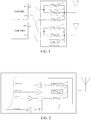
- 01 and 04 are receiving filters in the FDD frequency band
- 02 and 05 are transmitting filters in the FDD frequency band
- 03 and 06 are filters in the TDD frequency band
- this scheme connects the two systems of two separate FDD and TDD radio frequency units together through an external multiplexer, but this scheme has difficulty in the engineering installation, and the cost is high.
- the other is a channel independent mode. As shown in FIG.
- the receiving filter 01' in the FDD frequency band, the transmitting filter 02' in the FDD frequency band and the filter 03' in the TDD frequency band are combined together, and this scheme only physically splices the TDD circuit and the FDD circuit together (for example, on one circuit board), without sharing the transmitting and receiving channels, and only places the two systems in the same housing, with the externally embodied form thereof being a radio frequency unit but the essence thereof being still two sets of independent systems.
- a front-end circuit for a mobile radio includes a first Frequency Division Duplexing (FDD) transmission path for a first FDD mobile radio system, where the first FDD transmission path includes a transmission amplifier and a duplexer that includes a transmission filter element; a first Time Division Duplexing (TDD) transmission path for a first TDD mobile radio system, where the first TDD transmission path includes a transmission amplifier; an antenna connection configured for connecting to the duplexer or to the first TDD transmission path; at least one transmission filter; and a switch configuration to connect the at least one transmission filter to the first FDD transmission path or to the first TDD transmission path.
- the first TDD mobile radio system and the first FDD mobile radio system use a same first frequency band.
- the embodiments of the present invention provide a multiplexer to solve the problem of how multi-mode signals share a transmitting channel, a receiving channel and a transceiving antenna as defined in the attached independent claims.
- a multiplexer set between a transceiving antenna and a receiving channel as well as a transmitting channel; wherein the transceiving antenna, the receiving channel and the transmitting channel are shared by signals of at least two modes, the multiplexer comprises:
- the signals of the at least two modes comprise signals of two modes that are frequency division duplexing signal and time division duplexing signal, respectively.
- the multiplexer further comprises a time division duplexing device configured to connect or isolate a transmitting filter module and a receiving filter module corresponding to the time division duplexing signal.
- the transmitting filter module and the receiving filter module corresponding to the time division duplexing signal are the same two filter modules, a first end of the time division duplexing device is connected to one of the two filter modules, a second end is connected to the other filter module of the two filter modules, and a third end is connected to the transmitting channel; or the third end is connected to the amplifier module corresponding to the time division duplexing signal.
- the time division duplexing device comprises a first radio frequency switch, a second radio frequency switch and a two-way radio frequency switch; a first end of the two-way radio frequency switch is connected to one of the two filter modules; another end of the two-way radio frequency switch is connected to a first end of one of the first and second radio frequency switches, or is neither connected to the first radio frequency switch nor to the second radio frequency switch; a second end of the first radio frequency switch is connected to the other filter module, and a second end of the second radio frequency module is connected to the transmitting channel; or a first end of the first radio frequency switch is connected to the other filter module, and a second end of the second radio frequency switch is connected to the amplifier module corresponding to the time division duplexing signal.
- the time division duplexing device comprises a first radio frequency switch, a second radio frequency switch and a circulator; one end of the circulator is connected to one of the two filter modules; the other end of the circulator is connected to a first end of one of the two radio frequency switches; a second end of the first radio frequency switch is connected to the other filter module, and a second end of the second radio frequency switch is connected to the transmitting channel; or the first radio frequency switch is connected to the other filter module, and the second radio frequency switch is connected to the amplifier module corresponding to the time division duplexing signal.
- each receiving filter module or each transmitting filter module comprises at least one filter.
- the multiplexer provided in the embodiments of the present invention makes the transceiving antenna, the receiving channel and the transmitting channel shared by signals of at least two modes, wherein taking the multiplexer provided within the radio frequency unit for example, it can achieve sharing the transceiving antenna, the receiving channel and the transmitting channel of the radio frequency unit in the FDD and TDD modes, such that the sharing of analog and digital parts in the radio frequency unit become a reality.
- the multiplexer provided in the embodiments of the present invention can support signals of at least two modes, including but not limited to a FDD signal and TDD signal.
- the transceiving antenna, the receiving channel and the transmitting channel of the device where the multiplexer is located are shared by the signals of at least two modes, that is, the signals to be transmitted by the transmitting channel of the device where the multiplexer is located, as well as the signals received by the transceiving antenna and the receiving channel are signals of at least two modes; after the signals to be transmitted by the transmitting channel are selected by the respective transmitting filter modules corresponding to the signals of the various modes, a signal of the corresponding mode can be selected and then is transmitted through the transceiving antenna; after the signals received by the transceiving antenna are selected by the respective receiving filter modules corresponding to the signals of the various modes, a signal of the corresponding mode can be selected out and then is combined by the combiner module and transmitted to the receiving channel.
- Each receiving or transmitting filter module in the embodiments of the present invention comprises at least one filter, the number of filters in each filter module can be selected according to specifications of the filters and space and arrangement requirements of circuit boards, and each filter comprises but is not limited to a surface acoustic wave (SAW) filter, a dielectric filter, a cavity filter, and so on.
- the combiner module comprises but is not limited to a combiner.
- the amplifier module comprises but is not limited to an amplifier, and the amplifier may be a low noise amplifier mainly used for amplifying the received signals, helping the subsequent circuits to demodulate the received signals. Materials of various filters, amplifier, time division duplexing device and combiner are selected according to the specifications, and the space and arrangement requirements of circuit boards.
- FIG. 3 is a schematic diagram of a multiplexer provided in one embodiment of the present invention, and referring to FIG. 3 : the multiplexer provided in the present embodiment is used for transmitting and receiving FDD and TDD signals, and comprises: a combiner 101, a first receiving filter 102 corresponding to the FDD signal, a first amplifier 103 connected between the first receiving filter 102 and the combiner 101, a first transmitting filter 104 corresponding to the FDD signal, a filter 105 corresponding to the TDD signal, a second transmitting filter 106 corresponding to the TDD signal, a time division duplexing device 108, a second amplifier 107 connected between the time division duplexing device 108 and the combiner 101; a first end of the time division duplexing device 108 is connected to the filter 105, a second end is connected to the second transmitting filter 106, and a third end is connected to the second amplifier 107, the time division duplexing device 108 is configured to connect one of the second and third ends to the first end,
- the filter 105 corresponding to the TDD signal and the second transmitting filter 106 may be the same filters, and since the filter 105 corresponding to the TDD signal is arranged between the time division duplexing device 108 and the transceiving antenna, it also plays a role in transmitting the TDD signal in the present embodiment.
- the multiplexer has three external ports: P_Tx, P_Rx and P_ANT, wherein, the P_Tx is connected to a shared transmitting channel, and there are FDD-mode and TDD signals to be transmitted on the transmitting channel, and the signals are input to the multiplexer via this port; the P_ANT is connected to the transceiving antenna; the P_Rx is connected to the shared receiving channel and receive signals via the transceiving antenna, and after resisting blocking filtering and being low-noise amplified, respectively, the signals are input to the receiving channel via this port which is an uplink receiving output end of the multiplexer.
- the multiplexer 10 provided in the present embodiment may be built in the radio frequency unit, or may be independent of the radio frequency unit.
- the multiplexer provided in the present embodiment can work alone in the TDD mode, or work alone in the FDD mode, or work in the TDD/FDD dual-mode mode.
- the specific working modes are as follows:
- TDD downlink transmitting signals are to be transmitted on the shared transmitting channel
- the time division duplexing device 108 connects the TDD downlink transmitting link (i.e., connects the link between the second transmitting filter 106 and the filter 105), and disconnects the TDD uplink receiving link (i.e., disconnects the link between the filter 105 and the second amplifier 107)
- the TDD downlink transmitting signals enter the multiplexer via the P_Tx port, and are transmitted to the P_ANT port via the second transmitting filter 106, the time division duplexing device 108 and the filter 105, and then are transmitted to the transceiving antenna.
- Uplink receiving process TDD uplink receiving signals are received by the transceiving antenna, the time division duplexing device 108 connects the TDD uplink receiving link (i.e., connects the link between the filter 105 and the second amplifier 107), and disconnects the TDD downlink transmitting link (i.e., disconnects the link between the second transmitting filter 106 and the filter 105), the TDD uplink receiving signals enter the multiplexer via the P_ANT port, and then are input into the P_Rx port via the filter 105, the time division duplexing device 108, the second amplifier 107 and the combiner 101, and enter the shared receiving channel.
- Downlink transmitting process FDD downlink transmitting signals are to be transmitted on the shared transmitting channel, the time division duplexing device 108 disconnects the TDD uplink receiving link and the TDD downlink transmitting link, the FDD downlink transmitting signals enter the multiplexer via the P_Tx port, and then are transmitted to the P_ANT port via the first transmitting filter 104 and are transmitted to the transceiving antenna.
- Uplink receiving process FDD uplink receiving signals are received by the transceiving antenna are, the time division duplexing device 108 disconnects the TDD uplink receiving link and the TDD downlink transmitting link, the FDD uplink receiving signals enter the multiplexer port via the P_ANT port, and then are input into the P_Rx port via the first receiving filter 102, the first amplifier 103 and the combiner 101 and enter the shared receiving channel.
- TDD/FDD downlink transmitting dual-mode signals are to be transmitted on the shared transmitting channel
- the time division duplexing device 108 connects the TDD downlink transmitting link (i.e., connects the link between the second transmitting filter 106 and the filter 105), and disconnects the TDD uplink receiving link (i.e., disconnects the link between the filter 105 and the second amplifier 107)
- the TDD/FDD downlink transmitting dual-mode signals enter the multiplexer via the P_Tx port, and enter the first transmitting filter 104 and the second transmitting filter 106, respectively
- the FDD signals are selected out after filtered by the first transmitting filter 104, and are transmitted to the P_ANT port and then transmitted to the transceiving antenna
- the TDD signals are selected out after filtered by the second transmitting filter 106, and are transmitted to the P_ANT port via the time division duplexing device 108 and the filter 105 and then are transmitted to the transceiving antenna.
- TDD/FDD uplink receiving dual-mode signals are received by the transceiving antenna, the time division duplexing device 108 connects the TDD uplink receiving link (i.e., connects the link between the filter 105 and the second amplifier 107), and disconnects the TDD downlink transmitting link (i.e., disconnects the link between the second transmitting filter 106 and the filter 105), and the TDD/FDD uplink receiving dual-mode signals enter the multiplexer via the P_ANT port, and then enter the first receiving filter 102 and the filter 105, respectively, and the FDD signals are selected out after filtered by the first receiving filter 102, are transmitted to the first amplifier 103 to be amplified and then are transmitted to the combiner 101 to be combined, are input into the P_Rx port, and enter the shared receiving channel; the TDD signals are selected out after filtered by the filter 105, and are input into the P_Rx port via the time division duplexing device 108, the second amplifier 107 and the combiner 101,
- the combiner 101 is configured to combine the FDD uplink receiving signals and the TDD uplink receiving signals, and transmit them into the shared receiving channel.
- the first receiving filter 102 is configured to select out the FDD signals in the uplink receiving direction, allow the FDD signals on the uplink receiving direction to pass through, totally reflect the TDD signals and the FDD signals in the downlink transmitting direction, and resist blocking filtering.
- the first amplifier 103 is configured to amplify the FDD signals selected out in the uplink receiving direction.
- the first transmitting filter 104 is configured to select out the FDD signals in the downlink transmitting direction, allow the FDD signals in the downlink transmitting direction to pass through, filter out the out-of-band stray to prevent the stray from passing through the P_ANT port to affect the FDD UL (Uplink) reception as well as the TDD UL reception; and totally reflect the TDD signals.
- the second transmitting filter 106 is configured to select out the TDD signals in the downlink transmitting direction, allow the TDD signals in the downlink transmitting direction to pass through and meanwhile totally reflect the FDD signals.
- the filter 105 is configured to select out the TDD signals, and suppress signals other than the TDD signals. In the uplink receiving direction, it selects out the TDD signals, allows the TDD signals to pass through and totally reflect the FDD signals; in the downlink transmitting direction, it further strengthens the role in filtering the stray out of the TDD transmission band, and shares the out-of-band suppression requirements of the second transmitting filter module 106.
- the second amplifier 107 is configured to amplify the selected-out TDD signals in the uplink receiving direction.
- the time division duplexing device 108 is configured to connect or isolate the filter 105 and the second transmitting filter 106 (as above, connect the link between the filter 105 and the second transmitting filter 106 at some moments, and disconnect the link between the filter 105 and the second transmitting filter 106 at some other moments), so as to meet the time division separation requirements of TDD; meanwhile, it is also used to guarantee interference isolation between the TDD link and the FDD link, and when the FDD downlink transmission and the TDD uplink reception proceed at the same time, the isolation role is enhanced to prevent: the FDD downlink transmitting signals from blocking the TDD uplink receiving signals, and the FDD downlink transmitting signals from spuriously interfering the TDD uplink reception in the TDD frequency band, and when TDD uplink reception proceeds, the isolation between the P_Tx port and the P_Rx port is strengthened.
- the receiving frequency band of the first receiving filter 102 may be 2500MHz-2570MHz
- the transmitting frequency band of the first transmitting filter 104 may be 2620MHz-2690MHz
- the receiving frequency band of the filter 105 or the transmitting frequency band of the second transmitting filter 106 may be 2575MHz-2615MHz
- all the filters can be dielectric filters.
- the filter 105 and the second transmission filter 106 switch their positions.
- the time division duplexing device 108 is configured between the filter 105, the second transmission filter 106 and the P_ANT port, that is, a first end of the time division duplexing device 108 is connected to the P_ANT port, a second end is connected to the filter 105, and a third end is connected to the second transmitting filter 106.
- the specific structure of the time division duplex device 108 can be selected from a single-pole switch or a PIN switch according to requirements such as switching frequency, isolation between circuits, and power, and the number of switches can be selected according to the inter-circuit isolation requirements.
- FIG. 4 is a schematic diagram of the multiplexer provided in another embodiment of the present invention, and referring to FIG. 4 : the difference between the multiplexer provided in the present embodiment and the multiplexer shown in FIG. 3 is that: the time division duplexing device 108 comprises two radio frequency switches 108a and 108b, and further comprises a two-way radio frequency switch 108c, and the radio frequency switches 108a and 108b are provided in the TDD downlink transmitting link and the TDD uplink receiving link, respectively, and the two-way radio frequency switch 108c is provided between the radio frequency switches 108a, 108b and the filter 15.
- the specific working modes are as follows:
- Downlink transmitting process TDD downlink transmitting signals are to be transmitted on the shared transmitting channel, the radio frequency switch 108a is closed while the radio frequency switch 108b is disconnected, the two-way radio frequency switch 108c connects the filter 105 to position 1, and the TDD downlink transmission signals are transmitted to the P_ANT port via the P_Tx port, the second transmitting filter 106, the radio frequency switch 108a, the position 1 of the two-way radio frequency switch 108c, and the filter 105, and then are transmitted to the transceiving antenna.
- Uplink receiving process TDD uplink receiving signals are received by the transceiving antenna, the radio frequency switch 108b is closed while the radio frequency switch 108a is disconnected, the two-way radio frequency switch 108c connects the filter 105 to position 2, and the TDD uplink receiving signals are input into the P_Rx port via the P_ANT port, the filter 105, the position 2 of the two-way radio frequency switch 108c, the radio frequency switch 108b, the second amplifier 107, and the combiner 101, and then enter the shared receiving channel.
- Downlink transmitting process FDD downlink transmitting signals are to be transmitted on the shared transmitting channel, the radio frequency switches 108a and 108b and the two-way radio frequency switch 108c are all disconnected, and the FDD downlink transmitting signals are transmitted to the P_ANT port via the P_Tx port and the first transmitting filter 104, and are transmitted to the transceiving antenna.
- Uplink receiving process FDD uplink receiving signals are received by the transceiving antenna, the radio frequency switches 108a and 108b and the two-way radio frequency switch 108c are all disconnected, and the FDD uplink receiving signals are input into the P_Rx port via the P_ANT port, the first receiving filter 102, the first amplifier 103 and the combiner 101, and enter the shared receiving channel.
- TDD/FDD downlink transmitting dual-mode signals are to be transmitted on the shared transmitting channel , the radio frequency switch 108a is closed while the radio frequency switch 108b is disconnected, the two-way radio frequency switch 108c connects the filter 105 to position 1, the TDD/FDD downlink transmitting dual-mode signals respectively enter the first transmitting filter 104 and the second transmitting filter 106 via the P_Tx port, and the FDD signals are selected out after filtered by the first transmitting filter 104, are transmitted to the P_ANT port and are transmitted to the transceiving antenna; the TDD signals are selected out after filtered by the second transmitting filter 106, and then are transmitted to the P_ANT port via the radio frequency switch 108a, the position 1 of the two-way radio frequency switch 108c, and the filter 105, and are transmitted to the transceiving antenna.
- Uplink receiving process TDD/FDD uplink receiving dual-mode signals are received by the transceiving antenna, the radio frequency switch 108b is closed while the radio frequency switch 108a is disconnected, the two-way radio frequency switch 108c connects the filter 105 to the position 2, the TDD/FDD uplink receiving dual-mode signals respectively enter the first receiving filter 102 and the filter 105 via the P_ANT port, are transmitted to the first amplifier 103 to be amplified after filtered by the first receiving filter 102, and then are transmitted to the combiner 101 to be combined, are input into the P_Rx port, and enter the shared receiving channel; after filtered by the filter 105, they are input into the P_Rx port via the position 2 of the two-way radio frequency switch 108c, the radio frequency switch 108b, the second amplifier 107 and the combiner 10, and then enter the shared receiving channel.
- the filter 105 and the second transmission filter 106 switch their positions.
- the filter 105 is configured between the second amplifier 107 and the radio frequency switch 108b, and the specifications of the second transmitting filter 106 are adjusted accordingly.
- FIG. 5 is a schematic diagram of the multiplexer provided in another embodiment of the present invention, and referring to FIG. 5 : the difference between the multiplexer provided in the present embodiment and the multiplexer shown in FIG. 4 is that: the time division duplexing device 108 further comprises a circulator 108c' in addition to two radio frequency switches 108a and 108b, and the radio frequency switches 108a and 108b are provided in the TDD downlink transmitting link and the TDD uplink receiving link, respectively, and the circulator 108c' is provided between the radio frequency switches 108a, 108b and the filter 15. Its working processes are the same as the multiplexer shown in FIG. 4 .
- each module/unit in the above embodiments may be realized in the form of hardware, or in the form of software function modules.
- the present invention is not limited to the combination of hardware and software in any specific form.
- the multiplexer provided in the embodiments of the present invention makes the transceiving antenna, the receiving channel and the transmitting channel shared by signals of at least two modes, for example, shared by the FDD mode and the TDD mode, and makes the sharing of analog and digital parts in the radio frequency unit a reality.
Landscapes
- Engineering & Computer Science (AREA)
- Computer Networks & Wireless Communication (AREA)
- Signal Processing (AREA)
- Transceivers (AREA)
Claims (7)
- Multiplexeur, établi entre une antenne de transmission et un canal de réception ainsi qu'un canal de transmission ; dans lequel l'antenne de transmission, le canal de réception et le canal de transmission sont partagés par des signaux d'au moins deux modes, le multiplexeur comprend :une liaison de transmission et une liaison de réception correspondant à chacun des au moins deux modes, un module de filtre de transmission (104, 106) configuré sur la liaison de transmission correspondante, un module de filtre de réception (102, 105) et un module amplificateur (103, 107) configuré sur la liaison de réception correspondante ;dans lequel chaque module de filtre de transmission est configuré pour sélectionner un signal d'un mode correspondant parmi des signaux devant être transmis à travers le canal de transmission, et transmettre le signal du mode correspondant à l'antenne de transmission à travers la liaison de transmission correspondante ;chaque module de filtre de réception est configuré pour sélectionner un signal d'un mode correspondant parmi des signaux reçus par l'antenne de transmission, et transmettre le signal du mode correspondant au canal de réception à travers la liaison de réception correspondante ;chaque module amplificateur est configuré pour amplifier le signal du mode correspondant sélectionné par le module filtreur de réception connecté à celui-ci et transmettre le signal du mode correspondant au module combineur ;le multiplexeur comprend en outre un module combineur, le module combineur est configuré pour recevoir des signaux amplifiés par chaque module amplificateur, exécute un traitement de combinaison sur les signaux, et transmet le signal combiné au canal de réception.
- Multiplexeur selon la revendication 1, dans lequel les signaux de l'au moins deux modes comprennent des signaux de deux modes qui sont un signal de duplexage par répartition en fréquence et un signal de duplexage par répartition temporelle, respectivement.
- Multiplexeur selon la revendication 2, comprenant en outre :
un dispositif de duplexage par répartition temporelle, configuré pour connecter ou isoler un module de filtre de transmission et un module de filtre de réception correspondant au signal de duplexage par répartition temporelle. - Multiplexeur selon la revendication 3, dans lequel, le module de filtre de transmission (106) et le module de filtre de réception (105) correspondant au signal de duplexage par répartition temporelle sont les deux mêmes modules de filtre, une première extrémité du dispositif de duplexage par répartition temporelle est connectée à l'un des deux modules de filtre, une deuxième extrémité est connectée à l'autre module de filtre des deux modules de filtre, et une troisième extrémité est connectée au canal de transmission ; ou la troisième extrémité est connectée au module amplificateur correspondant au signal de duplexage par répartition temporelle.
- Multiplexeur selon la revendication 4, dans lequel, un dispositif de duplexage par répartition temporelle comprend une premier commutateur radio-fréquence (108a), un deuxième commutateur radio-fréquence (108b) et un commutateur radio-fréquence bidirectionnel (108c) ; une première extrémité du commutateur radio-fréquence bidirectionnel est connectée à l'un des deux modules de filtre ; une autre extrémité du commutateur radio-fréquence bidirectionnel est connectée à une première extrémité de l'un des premier et deuxième commutateurs radio-fréquence, ou n'est ni connectée au premier commutateur radio-fréquence ni au deuxième commutateur radio-fréquence ;
une deuxième extrémité du premier commutateur radio-fréquence est connectée à l'autre module de filtre, et une deuxième extrémité du deuxième module radio-fréquence est connectée au canal de transmission ;
ou une première extrémité du premier commutateur radio-fréquence est connectée à l'autre module de filtre, et une deuxième extrémité du deuxième commutateur radio-fréquence est connectée au module amplificateur correspondant au signal de duplexage par répartition temporelle. - Multiplexeur selon la revendication 4, dans lequel, le dispositif de duplexage par répartition temporelle comprend un premier commutateur radio-fréquence (108a), un deuxième commutateur radio-fréquence (108b) et un circulateur (108c) ; une extrémité du circulateur est connectée à l'un des deux modules de filtre ; l'autre extrémité du circulateur est connectée à une première extrémité de l'un des deux commutateurs radio-fréquence ;
une deuxième extrémité du premier commutateur radio-fréquence est connectée à l'autre module de filtre, et une deuxième extrémité du deuxième commutateur radio-fréquence est connectée au canal de transmission ;
ou le premier commutateur radio-fréquence est connecté à l'autre module de filtre, et le deuxième commutateur radio-fréquence est connecté au module amplificateur correspondant au signal de duplexage par répartition temporelle. - Multiplexeur selon l'une quelconque des revendications 1 à 6, dans lequel chaque module de filtre de réception ou chaque module de filtre de transmission comprend au moins un filtre.
Applications Claiming Priority (2)
| Application Number | Priority Date | Filing Date | Title |
|---|---|---|---|
| CN201210475369.9A CN103840851A (zh) | 2012-11-21 | 2012-11-21 | 一种多工器 |
| PCT/CN2013/081987 WO2013189404A1 (fr) | 2012-11-21 | 2013-08-21 | Multiplexeur |
Publications (3)
| Publication Number | Publication Date |
|---|---|
| EP2911305A1 EP2911305A1 (fr) | 2015-08-26 |
| EP2911305A4 EP2911305A4 (fr) | 2015-11-25 |
| EP2911305B1 true EP2911305B1 (fr) | 2018-11-07 |
Family
ID=49768141
Family Applications (1)
| Application Number | Title | Priority Date | Filing Date |
|---|---|---|---|
| EP13807022.2A Active EP2911305B1 (fr) | 2012-11-21 | 2013-08-21 | Multiplexeur |
Country Status (5)
| Country | Link |
|---|---|
| US (1) | US9559730B2 (fr) |
| EP (1) | EP2911305B1 (fr) |
| CN (1) | CN103840851A (fr) |
| ES (1) | ES2710521T3 (fr) |
| WO (1) | WO2013189404A1 (fr) |
Families Citing this family (19)
| Publication number | Priority date | Publication date | Assignee | Title |
|---|---|---|---|---|
| CN103840851A (zh) * | 2012-11-21 | 2014-06-04 | 中兴通讯股份有限公司 | 一种多工器 |
| KR102207866B1 (ko) * | 2014-04-01 | 2021-01-26 | 삼성전자주식회사 | 통신 서비스를 제공하기 위한 전자 장치 및 방법 |
| US9929768B2 (en) * | 2015-01-26 | 2018-03-27 | Huawei Technologies Co., Ltd. | System and method for TDD-FDD duplexing in a radio architecture |
| US10142086B2 (en) * | 2015-06-11 | 2018-11-27 | At&T Intellectual Property I, L.P. | Repeater and methods for use therewith |
| US9608692B2 (en) | 2015-06-11 | 2017-03-28 | At&T Intellectual Property I, L.P. | Repeater and methods for use therewith |
| US9912027B2 (en) | 2015-07-23 | 2018-03-06 | At&T Intellectual Property I, L.P. | Method and apparatus for exchanging communication signals |
| CN106936463B (zh) * | 2015-12-30 | 2020-04-24 | 中兴通讯股份有限公司 | 双工滤波装置、rru系统及无线射频系统 |
| CN107800459B (zh) * | 2016-08-31 | 2020-06-02 | 中国电信股份有限公司 | 用于跨频段载波聚合的射频拉远单元rru及合路方法 |
| US10811767B2 (en) | 2016-10-21 | 2020-10-20 | At&T Intellectual Property I, L.P. | System and dielectric antenna with convex dielectric radome |
| CN107069152A (zh) * | 2017-03-21 | 2017-08-18 | 南京米乐为微电子科技有限公司 | 一种毫米波超宽带大功率高隔离度集成单刀双掷开关 |
| CN117749235A (zh) * | 2018-07-23 | 2024-03-22 | Oppo广东移动通信有限公司 | 接收模组、射频系统及电子设备 |
| CN109104213A (zh) * | 2018-10-12 | 2018-12-28 | 中国电子科技集团公司第七研究所 | 一种支持tdd和fdd工作方式的有源天线tr组件 |
| JP7092716B2 (ja) * | 2019-08-07 | 2022-06-28 | 日立Astemo株式会社 | 信号伝送回路、信号伝送システム |
| CN112532268B (zh) * | 2019-09-19 | 2023-10-20 | 中兴通讯股份有限公司 | 一种通信电路及通信设备 |
| CN114614851B (zh) * | 2020-12-08 | 2024-05-28 | Oppo广东移动通信有限公司 | 信号收发电路、射频系统以及移动终端 |
| CN114520663A (zh) * | 2022-02-07 | 2022-05-20 | Oppo广东移动通信有限公司 | 信号发射装置及射频前端模块、设备 |
| CN114759935B (zh) * | 2022-04-08 | 2024-01-30 | 深圳英智源智能系统有限公司 | 一种智能多路复用器及信号控制方法 |
| JP2025536100A (ja) * | 2022-11-18 | 2025-10-30 | 華為技術有限公司 | マルチプレクサ及び通信装置 |
| CN119231191B (zh) * | 2023-06-30 | 2025-12-26 | 广州极飞科技股份有限公司 | 一种多合一天线模块、多合一天线系统以及无人设备 |
Family Cites Families (17)
| Publication number | Priority date | Publication date | Assignee | Title |
|---|---|---|---|---|
| US6307868B1 (en) * | 1995-08-25 | 2001-10-23 | Terayon Communication Systems, Inc. | Apparatus and method for SCDMA digital data transmission using orthogonal codes and a head end modem with no tracking loops |
| US6212172B1 (en) * | 1998-05-08 | 2001-04-03 | Omnipoint Corporation | Filtering method to allow FDD and TDD operation in PCS transreceivers |
| US7986742B2 (en) * | 2002-10-25 | 2011-07-26 | Qualcomm Incorporated | Pilots for MIMO communication system |
| US7493141B2 (en) * | 2004-03-15 | 2009-02-17 | Samsung Electronics Co., Ltd. | Common radio architecture for multi-mode multi-band applications |
| CN1917685A (zh) | 2005-08-17 | 2007-02-21 | 三星电子株式会社 | 多模式/多频带无线收发器 |
| CN101150359A (zh) * | 2006-09-19 | 2008-03-26 | 普天信息技术研究院 | 一种时分双工射频收发信机的实现方法和装置 |
| DE102008003820B4 (de) * | 2008-01-10 | 2013-01-17 | Epcos Ag | Frontendschaltung |
| US8503572B2 (en) * | 2009-02-02 | 2013-08-06 | Qualcomm Incorporated | Antenna virtualization in a wireless communication environment |
| US8432824B2 (en) * | 2009-05-01 | 2013-04-30 | Qualcomm Incorporated | Method and apparatus for selecting a receiving apparatus for co-channel operation |
| US9509543B2 (en) * | 2009-06-26 | 2016-11-29 | Qualcomm Incorporated | Method and apparatus that facilitates interference reduction in wireless systems |
| US8149742B1 (en) | 2009-06-26 | 2012-04-03 | Rockwell Collins, Inc. | System and method for receiving and transmitting signals |
| CN102056346B (zh) * | 2009-11-02 | 2013-11-06 | 中国移动通信集团公司 | 一种支持不同双工方式的基站 |
| CN201830256U (zh) * | 2010-06-24 | 2011-05-11 | 大唐移动通信设备有限公司 | 一种多通道的收信机装置 |
| CN102457992A (zh) * | 2010-10-19 | 2012-05-16 | 中国移动通信集团公司 | 一种基站设备 |
| US8971220B2 (en) * | 2010-12-02 | 2015-03-03 | Rockstar Consortium Us Lp | Dual mode base station |
| CN102404021A (zh) * | 2011-11-04 | 2012-04-04 | 中兴通讯股份有限公司 | 双工放大模块、射频前端模块和多模终端 |
| CN103840851A (zh) * | 2012-11-21 | 2014-06-04 | 中兴通讯股份有限公司 | 一种多工器 |
-
2012
- 2012-11-21 CN CN201210475369.9A patent/CN103840851A/zh active Pending
-
2013
- 2013-08-21 WO PCT/CN2013/081987 patent/WO2013189404A1/fr not_active Ceased
- 2013-08-21 US US14/646,289 patent/US9559730B2/en active Active
- 2013-08-21 EP EP13807022.2A patent/EP2911305B1/fr active Active
- 2013-08-21 ES ES13807022T patent/ES2710521T3/es active Active
Non-Patent Citations (1)
| Title |
|---|
| None * |
Also Published As
| Publication number | Publication date |
|---|---|
| ES2710521T3 (es) | 2019-04-25 |
| EP2911305A4 (fr) | 2015-11-25 |
| WO2013189404A1 (fr) | 2013-12-27 |
| US20150303951A1 (en) | 2015-10-22 |
| EP2911305A1 (fr) | 2015-08-26 |
| CN103840851A (zh) | 2014-06-04 |
| US9559730B2 (en) | 2017-01-31 |
Similar Documents
| Publication | Publication Date | Title |
|---|---|---|
| EP2911305B1 (fr) | Multiplexeur | |
| US11223384B2 (en) | Low noise signal chain architecture | |
| TWI683479B (zh) | 用於多頻帶射頻信號路由之裝置與方法 | |
| US9231552B2 (en) | RF front-end module and mobile wireless terminal | |
| KR101840879B1 (ko) | 고주파 수동 소자를 이용한 rf 송수신기의 전치단 장치 | |
| TWI729112B (zh) | 具有可切換雙工器的前端架構 | |
| US20140038531A1 (en) | High-frequency front-end circuit | |
| US20200295818A1 (en) | Multiple antenna repeater architecture | |
| US11349510B2 (en) | Radio frequency front end module and communication device | |
| CN101583206B (zh) | 一种td-scdma双卡双待移动终端 | |
| US20230344461A1 (en) | Radio frequency circuit and electronic device | |
| US20200067542A1 (en) | Radio frequency front end module and radio frequency signal processing method | |
| US20210006274A1 (en) | Radio frequency front end circuit and communication device | |
| US20170302317A1 (en) | High frequency front-end circuit and communication device | |
| EP3086477B1 (fr) | Système d'antenne, structure de communication intégrée et terminal | |
| KR101400739B1 (ko) | 무전기 간섭신호 제거 장치 | |
| US9768838B2 (en) | Reconfigurable RF receive diplexer | |
| US9929752B2 (en) | RF receive diplexer | |
| CN217282934U (zh) | 一种射频前端模组、系统 | |
| WO2015081513A1 (fr) | Filtre partiellement accordable et unité radio l'utilisant | |
| EP4578105A1 (fr) | Systèmes, appareils et procédés pour filtres d'émetteur-récepteur |
Legal Events
| Date | Code | Title | Description |
|---|---|---|---|
| PUAI | Public reference made under article 153(3) epc to a published international application that has entered the european phase |
Free format text: ORIGINAL CODE: 0009012 |
|
| 17P | Request for examination filed |
Effective date: 20150519 |
|
| AK | Designated contracting states |
Kind code of ref document: A1 Designated state(s): AL AT BE BG CH CY CZ DE DK EE ES FI FR GB GR HR HU IE IS IT LI LT LU LV MC MK MT NL NO PL PT RO RS SE SI SK SM TR |
|
| AX | Request for extension of the european patent |
Extension state: BA ME |
|
| RA4 | Supplementary search report drawn up and despatched (corrected) |
Effective date: 20151027 |
|
| RIC1 | Information provided on ipc code assigned before grant |
Ipc: H04B 1/40 20150101AFI20151021BHEP |
|
| DAX | Request for extension of the european patent (deleted) | ||
| GRAP | Despatch of communication of intention to grant a patent |
Free format text: ORIGINAL CODE: EPIDOSNIGR1 |
|
| STAA | Information on the status of an ep patent application or granted ep patent |
Free format text: STATUS: GRANT OF PATENT IS INTENDED |
|
| INTG | Intention to grant announced |
Effective date: 20180528 |
|
| GRAS | Grant fee paid |
Free format text: ORIGINAL CODE: EPIDOSNIGR3 |
|
| GRAA | (expected) grant |
Free format text: ORIGINAL CODE: 0009210 |
|
| STAA | Information on the status of an ep patent application or granted ep patent |
Free format text: STATUS: THE PATENT HAS BEEN GRANTED |
|
| AK | Designated contracting states |
Kind code of ref document: B1 Designated state(s): AL AT BE BG CH CY CZ DE DK EE ES FI FR GB GR HR HU IE IS IT LI LT LU LV MC MK MT NL NO PL PT RO RS SE SI SK SM TR |
|
| REG | Reference to a national code |
Ref country code: GB Ref legal event code: FG4D |
|
| REG | Reference to a national code |
Ref country code: CH Ref legal event code: EP Ref country code: AT Ref legal event code: REF Ref document number: 1063312 Country of ref document: AT Kind code of ref document: T Effective date: 20181115 |
|
| REG | Reference to a national code |
Ref country code: IE Ref legal event code: FG4D |
|
| REG | Reference to a national code |
Ref country code: DE Ref legal event code: R096 Ref document number: 602013046397 Country of ref document: DE |
|
| REG | Reference to a national code |
Ref country code: NL Ref legal event code: MP Effective date: 20181107 |
|
| REG | Reference to a national code |
Ref country code: LT Ref legal event code: MG4D |
|
| REG | Reference to a national code |
Ref country code: AT Ref legal event code: MK05 Ref document number: 1063312 Country of ref document: AT Kind code of ref document: T Effective date: 20181107 |
|
| REG | Reference to a national code |
Ref country code: ES Ref legal event code: FG2A Ref document number: 2710521 Country of ref document: ES Kind code of ref document: T3 Effective date: 20190425 |
|
| PG25 | Lapsed in a contracting state [announced via postgrant information from national office to epo] |
Ref country code: IS Free format text: LAPSE BECAUSE OF FAILURE TO SUBMIT A TRANSLATION OF THE DESCRIPTION OR TO PAY THE FEE WITHIN THE PRESCRIBED TIME-LIMIT Effective date: 20190307 Ref country code: BG Free format text: LAPSE BECAUSE OF FAILURE TO SUBMIT A TRANSLATION OF THE DESCRIPTION OR TO PAY THE FEE WITHIN THE PRESCRIBED TIME-LIMIT Effective date: 20190207 Ref country code: LT Free format text: LAPSE BECAUSE OF FAILURE TO SUBMIT A TRANSLATION OF THE DESCRIPTION OR TO PAY THE FEE WITHIN THE PRESCRIBED TIME-LIMIT Effective date: 20181107 Ref country code: HR Free format text: LAPSE BECAUSE OF FAILURE TO SUBMIT A TRANSLATION OF THE DESCRIPTION OR TO PAY THE FEE WITHIN THE PRESCRIBED TIME-LIMIT Effective date: 20181107 Ref country code: AT Free format text: LAPSE BECAUSE OF FAILURE TO SUBMIT A TRANSLATION OF THE DESCRIPTION OR TO PAY THE FEE WITHIN THE PRESCRIBED TIME-LIMIT Effective date: 20181107 Ref country code: NO Free format text: LAPSE BECAUSE OF FAILURE TO SUBMIT A TRANSLATION OF THE DESCRIPTION OR TO PAY THE FEE WITHIN THE PRESCRIBED TIME-LIMIT Effective date: 20190207 Ref country code: LV Free format text: LAPSE BECAUSE OF FAILURE TO SUBMIT A TRANSLATION OF THE DESCRIPTION OR TO PAY THE FEE WITHIN THE PRESCRIBED TIME-LIMIT Effective date: 20181107 Ref country code: FI Free format text: LAPSE BECAUSE OF FAILURE TO SUBMIT A TRANSLATION OF THE DESCRIPTION OR TO PAY THE FEE WITHIN THE PRESCRIBED TIME-LIMIT Effective date: 20181107 |
|
| PG25 | Lapsed in a contracting state [announced via postgrant information from national office to epo] |
Ref country code: SE Free format text: LAPSE BECAUSE OF FAILURE TO SUBMIT A TRANSLATION OF THE DESCRIPTION OR TO PAY THE FEE WITHIN THE PRESCRIBED TIME-LIMIT Effective date: 20181107 Ref country code: AL Free format text: LAPSE BECAUSE OF FAILURE TO SUBMIT A TRANSLATION OF THE DESCRIPTION OR TO PAY THE FEE WITHIN THE PRESCRIBED TIME-LIMIT Effective date: 20181107 Ref country code: RS Free format text: LAPSE BECAUSE OF FAILURE TO SUBMIT A TRANSLATION OF THE DESCRIPTION OR TO PAY THE FEE WITHIN THE PRESCRIBED TIME-LIMIT Effective date: 20181107 Ref country code: GR Free format text: LAPSE BECAUSE OF FAILURE TO SUBMIT A TRANSLATION OF THE DESCRIPTION OR TO PAY THE FEE WITHIN THE PRESCRIBED TIME-LIMIT Effective date: 20190208 Ref country code: PT Free format text: LAPSE BECAUSE OF FAILURE TO SUBMIT A TRANSLATION OF THE DESCRIPTION OR TO PAY THE FEE WITHIN THE PRESCRIBED TIME-LIMIT Effective date: 20190307 Ref country code: NL Free format text: LAPSE BECAUSE OF FAILURE TO SUBMIT A TRANSLATION OF THE DESCRIPTION OR TO PAY THE FEE WITHIN THE PRESCRIBED TIME-LIMIT Effective date: 20181107 |
|
| PG25 | Lapsed in a contracting state [announced via postgrant information from national office to epo] |
Ref country code: CZ Free format text: LAPSE BECAUSE OF FAILURE TO SUBMIT A TRANSLATION OF THE DESCRIPTION OR TO PAY THE FEE WITHIN THE PRESCRIBED TIME-LIMIT Effective date: 20181107 Ref country code: DK Free format text: LAPSE BECAUSE OF FAILURE TO SUBMIT A TRANSLATION OF THE DESCRIPTION OR TO PAY THE FEE WITHIN THE PRESCRIBED TIME-LIMIT Effective date: 20181107 Ref country code: PL Free format text: LAPSE BECAUSE OF FAILURE TO SUBMIT A TRANSLATION OF THE DESCRIPTION OR TO PAY THE FEE WITHIN THE PRESCRIBED TIME-LIMIT Effective date: 20181107 |
|
| REG | Reference to a national code |
Ref country code: DE Ref legal event code: R097 Ref document number: 602013046397 Country of ref document: DE |
|
| PG25 | Lapsed in a contracting state [announced via postgrant information from national office to epo] |
Ref country code: SM Free format text: LAPSE BECAUSE OF FAILURE TO SUBMIT A TRANSLATION OF THE DESCRIPTION OR TO PAY THE FEE WITHIN THE PRESCRIBED TIME-LIMIT Effective date: 20181107 Ref country code: EE Free format text: LAPSE BECAUSE OF FAILURE TO SUBMIT A TRANSLATION OF THE DESCRIPTION OR TO PAY THE FEE WITHIN THE PRESCRIBED TIME-LIMIT Effective date: 20181107 Ref country code: SK Free format text: LAPSE BECAUSE OF FAILURE TO SUBMIT A TRANSLATION OF THE DESCRIPTION OR TO PAY THE FEE WITHIN THE PRESCRIBED TIME-LIMIT Effective date: 20181107 Ref country code: RO Free format text: LAPSE BECAUSE OF FAILURE TO SUBMIT A TRANSLATION OF THE DESCRIPTION OR TO PAY THE FEE WITHIN THE PRESCRIBED TIME-LIMIT Effective date: 20181107 |
|
| PLBE | No opposition filed within time limit |
Free format text: ORIGINAL CODE: 0009261 |
|
| STAA | Information on the status of an ep patent application or granted ep patent |
Free format text: STATUS: NO OPPOSITION FILED WITHIN TIME LIMIT |
|
| 26N | No opposition filed |
Effective date: 20190808 |
|
| PG25 | Lapsed in a contracting state [announced via postgrant information from national office to epo] |
Ref country code: SI Free format text: LAPSE BECAUSE OF FAILURE TO SUBMIT A TRANSLATION OF THE DESCRIPTION OR TO PAY THE FEE WITHIN THE PRESCRIBED TIME-LIMIT Effective date: 20181107 |
|
| PG25 | Lapsed in a contracting state [announced via postgrant information from national office to epo] |
Ref country code: TR Free format text: LAPSE BECAUSE OF FAILURE TO SUBMIT A TRANSLATION OF THE DESCRIPTION OR TO PAY THE FEE WITHIN THE PRESCRIBED TIME-LIMIT Effective date: 20181107 |
|
| GBPC | Gb: european patent ceased through non-payment of renewal fee |
Effective date: 20190821 |
|
| PG25 | Lapsed in a contracting state [announced via postgrant information from national office to epo] |
Ref country code: LI Free format text: LAPSE BECAUSE OF NON-PAYMENT OF DUE FEES Effective date: 20190831 Ref country code: MC Free format text: LAPSE BECAUSE OF FAILURE TO SUBMIT A TRANSLATION OF THE DESCRIPTION OR TO PAY THE FEE WITHIN THE PRESCRIBED TIME-LIMIT Effective date: 20181107 Ref country code: LU Free format text: LAPSE BECAUSE OF NON-PAYMENT OF DUE FEES Effective date: 20190821 Ref country code: CH Free format text: LAPSE BECAUSE OF NON-PAYMENT OF DUE FEES Effective date: 20190831 |
|
| REG | Reference to a national code |
Ref country code: BE Ref legal event code: MM Effective date: 20190831 |
|
| PG25 | Lapsed in a contracting state [announced via postgrant information from national office to epo] |
Ref country code: IE Free format text: LAPSE BECAUSE OF NON-PAYMENT OF DUE FEES Effective date: 20190821 Ref country code: FR Free format text: LAPSE BECAUSE OF NON-PAYMENT OF DUE FEES Effective date: 20190831 |
|
| PG25 | Lapsed in a contracting state [announced via postgrant information from national office to epo] |
Ref country code: BE Free format text: LAPSE BECAUSE OF NON-PAYMENT OF DUE FEES Effective date: 20190831 Ref country code: GB Free format text: LAPSE BECAUSE OF NON-PAYMENT OF DUE FEES Effective date: 20190821 |
|
| PG25 | Lapsed in a contracting state [announced via postgrant information from national office to epo] |
Ref country code: CY Free format text: LAPSE BECAUSE OF FAILURE TO SUBMIT A TRANSLATION OF THE DESCRIPTION OR TO PAY THE FEE WITHIN THE PRESCRIBED TIME-LIMIT Effective date: 20181107 |
|
| PG25 | Lapsed in a contracting state [announced via postgrant information from national office to epo] |
Ref country code: HU Free format text: LAPSE BECAUSE OF FAILURE TO SUBMIT A TRANSLATION OF THE DESCRIPTION OR TO PAY THE FEE WITHIN THE PRESCRIBED TIME-LIMIT; INVALID AB INITIO Effective date: 20130821 Ref country code: MT Free format text: LAPSE BECAUSE OF FAILURE TO SUBMIT A TRANSLATION OF THE DESCRIPTION OR TO PAY THE FEE WITHIN THE PRESCRIBED TIME-LIMIT Effective date: 20181107 |
|
| PG25 | Lapsed in a contracting state [announced via postgrant information from national office to epo] |
Ref country code: MK Free format text: LAPSE BECAUSE OF FAILURE TO SUBMIT A TRANSLATION OF THE DESCRIPTION OR TO PAY THE FEE WITHIN THE PRESCRIBED TIME-LIMIT Effective date: 20181107 |
|
| PGFP | Annual fee paid to national office [announced via postgrant information from national office to epo] |
Ref country code: ES Payment date: 20250902 Year of fee payment: 13 |
|
| PGFP | Annual fee paid to national office [announced via postgrant information from national office to epo] |
Ref country code: DE Payment date: 20250624 Year of fee payment: 13 |
|
| PGFP | Annual fee paid to national office [announced via postgrant information from national office to epo] |
Ref country code: IT Payment date: 20250722 Year of fee payment: 13 |