EP2919045A1 - Light control panel fabrication method - Google Patents
Light control panel fabrication method Download PDFInfo
- Publication number
- EP2919045A1 EP2919045A1 EP13854159.4A EP13854159A EP2919045A1 EP 2919045 A1 EP2919045 A1 EP 2919045A1 EP 13854159 A EP13854159 A EP 13854159A EP 2919045 A1 EP2919045 A1 EP 2919045A1
- Authority
- EP
- European Patent Office
- Prior art keywords
- light control
- control panel
- sheets
- producing
- transparent
- Prior art date
- Legal status (The legal status is an assumption and is not a legal conclusion. Google has not performed a legal analysis and makes no representation as to the accuracy of the status listed.)
- Granted
Links
Images


Classifications
-
- G—PHYSICS
- G02—OPTICS
- G02B—OPTICAL ELEMENTS, SYSTEMS OR APPARATUS
- G02B5/00—Optical elements other than lenses
- G02B5/08—Mirrors
-
- B—PERFORMING OPERATIONS; TRANSPORTING
- B32—LAYERED PRODUCTS
- B32B—LAYERED PRODUCTS, i.e. PRODUCTS BUILT-UP OF STRATA OF FLAT OR NON-FLAT, e.g. CELLULAR OR HONEYCOMB, FORM
- B32B27/00—Layered products comprising a layer of synthetic resin
- B32B27/16—Layered products comprising a layer of synthetic resin specially treated, e.g. irradiated
-
- B—PERFORMING OPERATIONS; TRANSPORTING
- B32—LAYERED PRODUCTS
- B32B—LAYERED PRODUCTS, i.e. PRODUCTS BUILT-UP OF STRATA OF FLAT OR NON-FLAT, e.g. CELLULAR OR HONEYCOMB, FORM
- B32B27/00—Layered products comprising a layer of synthetic resin
- B32B27/30—Layered products comprising a layer of synthetic resin comprising vinyl (co)polymers; comprising acrylic (co)polymers
- B32B27/308—Layered products comprising a layer of synthetic resin comprising vinyl (co)polymers; comprising acrylic (co)polymers comprising acrylic (co)polymers
-
- B—PERFORMING OPERATIONS; TRANSPORTING
- B32—LAYERED PRODUCTS
- B32B—LAYERED PRODUCTS, i.e. PRODUCTS BUILT-UP OF STRATA OF FLAT OR NON-FLAT, e.g. CELLULAR OR HONEYCOMB, FORM
- B32B38/00—Ancillary operations in connection with laminating processes
- B32B38/0004—Cutting, tearing or severing, e.g. bursting; Cutter details
-
- B—PERFORMING OPERATIONS; TRANSPORTING
- B32—LAYERED PRODUCTS
- B32B—LAYERED PRODUCTS, i.e. PRODUCTS BUILT-UP OF STRATA OF FLAT OR NON-FLAT, e.g. CELLULAR OR HONEYCOMB, FORM
- B32B7/00—Layered products characterised by the relation between layers; Layered products characterised by the relative orientation of features between layers, or by the relative values of a measurable parameter between layers, i.e. products comprising layers having different physical, chemical or physicochemical properties; Layered products characterised by the interconnection of layers
- B32B7/04—Interconnection of layers
- B32B7/12—Interconnection of layers using interposed adhesives or interposed materials with bonding properties
-
- B—PERFORMING OPERATIONS; TRANSPORTING
- B32—LAYERED PRODUCTS
- B32B—LAYERED PRODUCTS, i.e. PRODUCTS BUILT-UP OF STRATA OF FLAT OR NON-FLAT, e.g. CELLULAR OR HONEYCOMB, FORM
- B32B9/00—Layered products comprising a layer of a particular substance not covered by groups B32B11/00 - B32B29/00
- B32B9/005—Layered products comprising a layer of a particular substance not covered by groups B32B11/00 - B32B29/00 comprising one layer of ceramic material, e.g. porcelain, ceramic tile
-
- G—PHYSICS
- G02—OPTICS
- G02B—OPTICAL ELEMENTS, SYSTEMS OR APPARATUS
- G02B30/00—Optical systems or apparatus for producing three-dimensional [3D] effects, e.g. stereoscopic images
- G02B30/20—Optical systems or apparatus for producing three-dimensional [3D] effects, e.g. stereoscopic images by providing first and second parallax images to an observer's left and right eyes
- G02B30/34—Stereoscopes providing a stereoscopic pair of separated images corresponding to parallactically displaced views of the same object, e.g. three-dimensional [3D] slide viewers
- G02B30/35—Stereoscopes providing a stereoscopic pair of separated images corresponding to parallactically displaced views of the same object, e.g. three-dimensional [3D] slide viewers using reflective optical elements in the optical path between the images and the observer
-
- G—PHYSICS
- G02—OPTICS
- G02B—OPTICAL ELEMENTS, SYSTEMS OR APPARATUS
- G02B30/00—Optical systems or apparatus for producing three-dimensional [3D] effects, e.g. stereoscopic images
- G02B30/50—Optical systems or apparatus for producing three-dimensional [3D] effects, e.g. stereoscopic images the image being built up from image elements distributed over a three-dimensional [3D] volume, e.g. voxels
- G02B30/56—Optical systems or apparatus for producing three-dimensional [3D] effects, e.g. stereoscopic images the image being built up from image elements distributed over a three-dimensional [3D] volume, e.g. voxels by projecting aerial or floating images
-
- G—PHYSICS
- G02—OPTICS
- G02B—OPTICAL ELEMENTS, SYSTEMS OR APPARATUS
- G02B5/00—Optical elements other than lenses
- G02B5/08—Mirrors
- G02B5/0816—Multilayer mirrors, i.e. having two or more reflecting layers
-
- G—PHYSICS
- G02—OPTICS
- G02B—OPTICAL ELEMENTS, SYSTEMS OR APPARATUS
- G02B5/00—Optical elements other than lenses
- G02B5/08—Mirrors
- G02B5/0816—Multilayer mirrors, i.e. having two or more reflecting layers
- G02B5/085—Multilayer mirrors, i.e. having two or more reflecting layers at least one of the reflecting layers comprising metal
-
- G—PHYSICS
- G03—PHOTOGRAPHY; CINEMATOGRAPHY; ANALOGOUS TECHNIQUES USING WAVES OTHER THAN OPTICAL WAVES; ELECTROGRAPHY; HOLOGRAPHY
- G03B—APPARATUS OR ARRANGEMENTS FOR TAKING PHOTOGRAPHS OR FOR PROJECTING OR VIEWING THEM; APPARATUS OR ARRANGEMENTS EMPLOYING ANALOGOUS TECHNIQUES USING WAVES OTHER THAN OPTICAL WAVES; ACCESSORIES THEREFOR
- G03B35/00—Stereoscopic photography
- G03B35/18—Stereoscopic photography by simultaneous viewing
-
- B—PERFORMING OPERATIONS; TRANSPORTING
- B32—LAYERED PRODUCTS
- B32B—LAYERED PRODUCTS, i.e. PRODUCTS BUILT-UP OF STRATA OF FLAT OR NON-FLAT, e.g. CELLULAR OR HONEYCOMB, FORM
- B32B2255/00—Coating on the layer surface
- B32B2255/20—Inorganic coating
- B32B2255/205—Metallic coating
-
- B—PERFORMING OPERATIONS; TRANSPORTING
- B32—LAYERED PRODUCTS
- B32B—LAYERED PRODUCTS, i.e. PRODUCTS BUILT-UP OF STRATA OF FLAT OR NON-FLAT, e.g. CELLULAR OR HONEYCOMB, FORM
- B32B2307/00—Properties of the layers or laminate
- B32B2307/40—Properties of the layers or laminate having particular optical properties
- B32B2307/412—Transparent
-
- B—PERFORMING OPERATIONS; TRANSPORTING
- B32—LAYERED PRODUCTS
- B32B—LAYERED PRODUCTS, i.e. PRODUCTS BUILT-UP OF STRATA OF FLAT OR NON-FLAT, e.g. CELLULAR OR HONEYCOMB, FORM
- B32B2307/00—Properties of the layers or laminate
- B32B2307/40—Properties of the layers or laminate having particular optical properties
- B32B2307/416—Reflective
-
- B—PERFORMING OPERATIONS; TRANSPORTING
- B32—LAYERED PRODUCTS
- B32B—LAYERED PRODUCTS, i.e. PRODUCTS BUILT-UP OF STRATA OF FLAT OR NON-FLAT, e.g. CELLULAR OR HONEYCOMB, FORM
- B32B2315/00—Other materials containing non-metallic inorganic compounds not provided for in groups B32B2311/00 - B32B2313/04
- B32B2315/08—Glass
-
- B—PERFORMING OPERATIONS; TRANSPORTING
- B32—LAYERED PRODUCTS
- B32B—LAYERED PRODUCTS, i.e. PRODUCTS BUILT-UP OF STRATA OF FLAT OR NON-FLAT, e.g. CELLULAR OR HONEYCOMB, FORM
- B32B2551/00—Optical elements
-
- B—PERFORMING OPERATIONS; TRANSPORTING
- B32—LAYERED PRODUCTS
- B32B—LAYERED PRODUCTS, i.e. PRODUCTS BUILT-UP OF STRATA OF FLAT OR NON-FLAT, e.g. CELLULAR OR HONEYCOMB, FORM
- B32B2551/00—Optical elements
- B32B2551/08—Mirrors
-
- B—PERFORMING OPERATIONS; TRANSPORTING
- B32—LAYERED PRODUCTS
- B32B—LAYERED PRODUCTS, i.e. PRODUCTS BUILT-UP OF STRATA OF FLAT OR NON-FLAT, e.g. CELLULAR OR HONEYCOMB, FORM
- B32B2607/00—Walls, panels
-
- Y—GENERAL TAGGING OF NEW TECHNOLOGICAL DEVELOPMENTS; GENERAL TAGGING OF CROSS-SECTIONAL TECHNOLOGIES SPANNING OVER SEVERAL SECTIONS OF THE IPC; TECHNICAL SUBJECTS COVERED BY FORMER USPC CROSS-REFERENCE ART COLLECTIONS [XRACs] AND DIGESTS
- Y10—TECHNICAL SUBJECTS COVERED BY FORMER USPC
- Y10T—TECHNICAL SUBJECTS COVERED BY FORMER US CLASSIFICATION
- Y10T156/00—Adhesive bonding and miscellaneous chemical manufacture
- Y10T156/10—Methods of surface bonding and/or assembly therefor
- Y10T156/1052—Methods of surface bonding and/or assembly therefor with cutting, punching, tearing or severing
Definitions
- the present invention relates to a method for producing a light control panel for use in an optical imaging apparatus that forms a volumetric image in the air.
- Patent Literature 1 describes a technique to form an image of an object on the side opposite to the optical imaging apparatus by using a first light control panel and a second light control panel each formed by arranging, inside a transparent flat plate, a number of belt-like planar light-reflective portions perpendicularly to a surface on one side of the transparent flat plate, making one side of each of the first and the second light control panels face to face with each other in a manner that makes the planar light-reflective portions of the first light control panel and the planar light-reflective portions of the second light control panel orthogonal to one another, making light from the object (or a light source) incident upon the planar light-reflective portions of the first light control panel, and making reflected light reflected at these planar light-reflective portions re-reflect at the planar light-reflective portions of the second light control panel.
- Patent Literature 1 discloses making of a light control panel by making a laminated body through laminating a number of transparent synthetic resin plates (e.g., acrylic resin plates) or glass plates each having a metallic reflective surface consisting of a deposited layer (or a plated layer) of aluminum, silver or the like, which are examples of metals (the metallic reflective surface therefore becomes a both-sided reflective plate), formed on one surface side and each having a constant thickness in a manner that makes each metallic reflective surface arranged on one side, and through cutting out from this laminated body in a manner that forms a cut-out surface perpendicular to each metallic reflective surface.
- transparent synthetic resin plates e.g., acrylic resin plates
- glass plates each having a metallic reflective surface consisting of a deposited layer (or a plated layer) of aluminum, silver or the like, which are examples of metals (the metallic reflective surface therefore becomes a both-sided reflective plate), formed on one surface side and each having a constant thickness in a manner that makes each metallic reflective surface arranged on one side
- Patent Literature 2 also describes producing of light control panels by laminating a plurality of planar mirrors and cutting them in a longitudinal direction, and producing of a planar mirror by forming through methods such as one to deposit a metallic film such as tin, silver and aluminum on the surface of acrylic, glass and the like.
- the present invention has been made in view of the above circumstances, and an object thereof is to provide a method for producing a light control panel that is easily produced and for use in an optical imaging apparatus.
- a method for producing a light control panel according to the present invention for use in an optical imaging apparatus is a method for producing a first light control panel and a second light control panel of an optical imaging apparatus each formed by arranging belt-like planar light-reflective portions at a constant pitch inside a transparent flat plate, and arranging opposed to each other the first light control panel and the second light control panel in a manner that makes the planar light-reflective portions of the first light control panel and the planar light-reflective portions of the second light control panel cross one another, the method for producing a light control panel, including:
- the mirror sheets may be those in which metal is deposited on one side or both sides of thin glass plates. Additionally, the mirror sheets may be those in which metal is deposited on one side or both sides of thin resin plates, and depending on conditions, may be metallic plates (excluding copper and gold).
- a transparent adhesive agent for the joining of the transparent sheets and the mirror sheets it is preferable to use a transparent adhesive agent for the joining of the transparent sheets and the mirror sheets.
- the transparent adhesive agent it is preferable for the transparent adhesive agent to be a UV curing-type adhesive agent, and in this case, the UV curing-type adhesive agent is able to be cured by ultraviolet light irradiated from a direction orthogonal to the plate thickness of the transparent sheets.
- thermosetting-type adhesive agent may also be used as the adhesive agent, and the adhesive agent may be cured by induction heating, dielectric heating (microwaves), or furnace heating.
- the mirror sheets may be preliminarily attached to one side or both sides of the transparent sheets, and transparent sheets having mirrors to which the mirror sheets are attached may be laminated.
- the thickness of the transparent sheets in the range of 300 to 1000 ⁇ m, and for the thickness of the mirror sheets to be in the range of 30 to 100 ⁇ m. Easy inflection is allowed in these ranges even when mirror sheets are those in which metal having high light reflectivity such as aluminum and silver is deposited on one side or both sides of glass plates, and Ra value for the degree of mirror surface roughness stays low.
- the adhesive agent when a UV curing-type adhesive agent is used as the adhesive agent to join the transparent sheets and the mirror sheets, the adhesive agent can be cured by irradiating ultraviolet light from the lateral side of the block. Additionally, even when a thermosetting-type adhesive agent is used, the adhesive agent can be easily heated and cured by induction heating, microwaves, or furnace heating.
- the optical imaging apparatus 10 is produced by using a first light control panel 13 and a second light control panel 14 formed by arranging, inside two transparent flat plates in the thickness direction of the transparent flat plates, a number of belt-like planar light-reflective portions 11 and 12 consisting of metallic reflective surfaces (e.g., aluminum, silver, titanium, tin, etc.) at a constant pitch p1, and making one side of each of the first and the second light control panels 13 and 14 face to face and coherent with each other in a manner that makes the planar light-reflective portions 11 and the planar light-reflective portions 12 cross (e.g., orthogonal to) one another.
- the planar light-reflective portions 11 and 12 are arranged perpendicularly to the surfaces of the transparent flat plates, however, they may also be arranged inclined.
- the pitches p1 between the planar light-reflective portions 11 and between the planar light-reflective portions 12 each to be approximately 0.1- to 3-fold (more preferably, 0.1- to 2-fold, even more preferably, 0.2- to 0.5-fold) of the thicknesses t1 and t2 of the first and the second light control panels 13 and 14.
- the thicknesses t1 and t2 of the first and the second light control panels 13 and 14 vary depending on the intended use, they are in the range of 0.5 to 10 mm, the first and the second light control panels 13 and 14 each have, for example, 300 to 2000 pieces of the planar light-reflective portions 11 and 12.
- the optical imaging apparatus 10 having 90,000 to 4,000,000 picture elements can be obtained.
- the optical imaging apparatus 10 In the case of the optical imaging apparatus 10, light rays from a point a of an object N regularly reflect at points Q of the planar light-reflective portions 11 of the first light control panel 13, subsequently reflect at points Q' of the planar light-reflective portions 12 of the second light control panel 14, and become concentrated at a point a'.
- Light rays from a point b of the object N reflect at points R of the planar light-reflective portions 11 of the first light control panel 13, the light rays further reflect at points R' of the planar light-reflective portions 12 of the second light control panel 14 and become concentrated at a point b'. Therefore, by using this optical imaging apparatus 10, the object N forms a volumetric image N' at a position symmetrical about the optical imaging apparatus 10. Details on these techniques are described in WO 2009/131128 .
- the number of transparent sheets 16 required in accordance with the size of an optical imaging apparatus 10 to be produced is prepared.
- the thickness t3 of the transparent sheets 16 (e.g., 300 to 1000 ⁇ m) determines the pitches p1 between the planar light-reflective portions 11 and between the planar light-reflective portions 12.
- the transparent sheets 16 are preferably pieces of glass, however, can also be pieces of transparent plastic (e.g., acrylic resin), ceramic and the like.
- mirror sheets 17 with a thickness t4 of, for example, approximately 30 to 100 ⁇ m, and consisting of glass plates having a piece of metal excluding copper and gold deposited or plated on one side or both sides thereof are prepared in plurality.
- mirror sheets 17 are generally rolled in a roll shape, as illustrated in FIG. 3
- mirror sheets 17 in a rolled state having, for example, transparent UV-curable resin (an example of UV curing-type adhesive agents) applied on one side or both sides are prepared.
- transparent UV-curable resin an example of UV curing-type adhesive agents
- Each pitch p1 (distance) between the planar light-reflective portions 11 and between the planar light-reflective portions 12 of the first and the second light control panels 13 and 14 is a value in which the thickness t4 of one of the mirror sheets 17 is added to the thickness t3 of one of the transparent sheets 16, and when the adhesive agent has a thickness, the thickness of the adhesive agent becomes added as well.
- the predetermined number of the transparent sheets 16 having the mirror sheets 17 arranged thereon thereby become arranged in a stacked state.
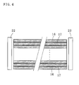
- the UV-curable resin becomes also applied on the surfaces of the mirror sheets 17 to come in direct contact with the other transparent sheets 16 at the time of laminating. Accordingly, as illustrated in FIG. 4 , the mirror sheets 17 and the transparent sheets 16 are alternately laminated, and ultraviolet light is irradiated from the ends of the transparent sheets 16 (i.e., from directions orthogonal to or crossing the laminated direction of the transparent sheets 16).
- Numerals 22 and 23 indicate ultraviolet lamps.
- the UV (ultraviolet)-curable resin thereby functions as an adhesive agent, and a block 19 in which the mirror sheets 17 and the transparent sheets 16 are alternately stacked becomes formed.
- the block 19 becomes cut on a surface crossing (e.g., orthogonal to) the transparent sheets 16 and the mirror sheets 17 in a manner that makes the thickness of a cutout constant by a cutter 20.
- the cutting angle ⁇ of the cutter 20 is made to be 90 degrees, however, depending on, for example, the intended purposes, other angles (e.g., 70 degrees ⁇ 90 degrees) can also be applied.
- the cutter 20 simply cutting the block 19 causes asperity in the cut surface, after the cutting, the surface becomes ground and polished to make the thicknesses of cutouts t1 and t2. A little accidental error in these thicknesses, t1 and t2, does not cause any problem in the function.
- the optical imaging apparatus 10 becomes completed.
- a transparent plate may be arranged in between the first and the second light control panels 13 and 14.
- the first and the second light control panels 13 and 14 are joined in a manner that makes each planar light-reflective portion 11 of the first light control panel 13 and each planar light-reflective portion 12 of the second light control panel 14 orthogonal to one another in planar view.
- an optical imaging apparatus can also be formed by making them cross at an angle that is smaller than 90 degrees.
- the position of a real image (volumetric image) becomes different, and in some cases, the real image (volumetric image) becomes enlarged or minified.
- the first and the second light control panels can also be made by, after preparing transparent sheets having mirrors made by preliminarily sticking (or joining) the mirror sheets 17 on (to) (either one side or both sides of) the transparent sheets 16, laminating these transparent sheets having mirrors by using an adhesive agent to make a block, and cutting the block in the thickness direction of the laminated body to a predetermined cutout thickness.
- the mirror sheets are those in which metal having reflectivity excluding copper and gold is deposited on the thin glass plates, however, thin plastic plates (resin plates) can be used in place of the thin glass plates, and depending on circumstances, thin metallic foils can be used alternatively.
- mirror surfaces of the mirror sheets metallic reflective surfaces
- the metallic reflective surfaces are formed only on one side, the glass plates or the plastic plates can be in direct contact with the transparent sheets.
- a UV curing-type adhesive agent is used, however, a regular adhesive agent can alternatively be used, and a thermosetting-type adhesive agent, a hot melt and the like can also be used alternatively.
- the present invention also applies to the case where an adhesive agent that becomes cured, in place of ultraviolet light irradiation, by means of infrared heating, far-infrared heating, induction heating or dielectric heating, and depending on circumstances, that becomes cured by being heated inside a furnace body (furnace heating) or in a normal temperature setting is used.
- the present invention is not limited to the above embodiment, and the present invention also applies to a case where the dimension and the shape are changed and a case where an additional new component is added within the range that does not alter the gist of the present invention.
- light control panels capable of forming a volumetric image as a real image can be produced at a low cost and in large quantity. These light control panels can be applied to displays of televisions, mobile phones, medical equipments and other uses.
Landscapes
- Physics & Mathematics (AREA)
- General Physics & Mathematics (AREA)
- Optics & Photonics (AREA)
- Chemical & Material Sciences (AREA)
- Engineering & Computer Science (AREA)
- Ceramic Engineering (AREA)
- Optical Elements Other Than Lenses (AREA)
- Joining Of Glass To Other Materials (AREA)
- Testing, Inspecting, Measuring Of Stereoscopic Televisions And Televisions (AREA)
Abstract
Description
- The present invention relates to a method for producing a light control panel for use in an optical imaging apparatus that forms a volumetric image in the air.
- As an optical imaging apparatus that forms a volumetric image by using light (scattering light) emitted from the surface of an object, Patent Literature 1 describes a technique to form an image of an object on the side opposite to the optical imaging apparatus by using a first light control panel and a second light control panel each formed by arranging, inside a transparent flat plate, a number of belt-like planar light-reflective portions perpendicularly to a surface on one side of the transparent flat plate, making one side of each of the first and the second light control panels face to face with each other in a manner that makes the planar light-reflective portions of the first light control panel and the planar light-reflective portions of the second light control panel orthogonal to one another, making light from the object (or a light source) incident upon the planar light-reflective portions of the first light control panel, and making reflected light reflected at these planar light-reflective portions re-reflect at the planar light-reflective portions of the second light control panel.
- Also, Patent Literature 1 discloses making of a light control panel by making a laminated body through laminating a number of transparent synthetic resin plates (e.g., acrylic resin plates) or glass plates each having a metallic reflective surface consisting of a deposited layer (or a plated layer) of aluminum, silver or the like, which are examples of metals (the metallic reflective surface therefore becomes a both-sided reflective plate), formed on one surface side and each having a constant thickness in a manner that makes each metallic reflective surface arranged on one side, and through cutting out from this laminated body in a manner that forms a cut-out surface perpendicular to each metallic reflective surface.
Additionally, Patent Literature 2 also describes producing of light control panels by laminating a plurality of planar mirrors and cutting them in a longitudinal direction, and producing of a planar mirror by forming through methods such as one to deposit a metallic film such as tin, silver and aluminum on the surface of acrylic, glass and the like. -
- Patent Literature 1:
WO 2009/131128 - Patent Literature 2: Japanese Unexamined Patent Application Publication No.
2011-081300 - However, producing light control panels by depositing a metallic reflective layer on the surface of a transparent synthetic resin plate, glass plate and the like requires a special deposition apparatus and is also time-consuming, there has been a problem of not being able to achieve inexpensive mass production. Moreover, sheets having metallic reflective surfaces formed thereon need to be laminated in large numbers in the end, which has made the work of laminating using an adhesive agent necessary.
- The present invention has been made in view of the above circumstances, and an object thereof is to provide a method for producing a light control panel that is easily produced and for use in an optical imaging apparatus. Solution to Problem
- In order to achieve the above object, a method for producing a light control panel according to the present invention for use in an optical imaging apparatus is a method for producing a first light control panel and a second light control panel of an optical imaging apparatus each formed by arranging belt-like planar light-reflective portions at a constant pitch inside a transparent flat plate, and arranging opposed to each other the first light control panel and the second light control panel in a manner that makes the planar light-reflective portions of the first light control panel and the planar light-reflective portions of the second light control panel cross one another, the method for producing a light control panel, including:
- a first step of forming a block in which transparent sheets made of glass, ceramic or transparent plastic and mirror sheets each having a metallic reflective surface on both sides or one side of a piece of metal, glass or resin are alternately stacked and laminated; and
- a second step of forming the first or the second light control panel by cutting out from the block on a surface crossing the transparent sheets and the mirror sheets in a manner that makes the thickness of a cutout constant.
- In the case of the method for producing a light control panel according to the present invention, the mirror sheets may be those in which metal is deposited on one side or both sides of thin glass plates. Additionally, the mirror sheets may be those in which metal is deposited on one side or both sides of thin resin plates, and depending on conditions, may be metallic plates (excluding copper and gold).
In the case of the method for producing a light control panel according to the present invention, it is preferable to use a transparent adhesive agent for the joining of the transparent sheets and the mirror sheets. Here, it is preferable for the transparent adhesive agent to be a UV curing-type adhesive agent, and in this case, the UV curing-type adhesive agent is able to be cured by ultraviolet light irradiated from a direction orthogonal to the plate thickness of the transparent sheets. - A thermosetting-type adhesive agent may also be used as the adhesive agent, and the adhesive agent may be cured by induction heating, dielectric heating (microwaves), or furnace heating.
- In the case of the method for producing a light control panel according to the present invention, the mirror sheets may be preliminarily attached to one side or both sides of the transparent sheets, and transparent sheets having mirrors to which the mirror sheets are attached may be laminated.
- In the case of the method for producing a light control panel according to the present invention, it is preferable for the thickness of the transparent sheets to be in the range of 300 to 1000 µm, and for the thickness of the mirror sheets to be in the range of 30 to 100 µm. Easy inflection is allowed in these ranges even when mirror sheets are those in which metal having high light reflectivity such as aluminum and silver is deposited on one side or both sides of glass plates, and Ra value for the degree of mirror surface roughness stays low. Advantageous Effects of Invention
- In the case of the method for producing a light control panel according to the present invention, since the mirror surfaces to be arranged between each transparent sheet is produced not by deposition but by using independent mirror sheets, the production process becomes extremely simplified, and light control panels can be produced at a low cost, thereby enabling the provision of an optical imaging apparatus that forms a volumetric image at a lower cost.
- Especially, when a UV curing-type adhesive agent is used as the adhesive agent to join the transparent sheets and the mirror sheets, the adhesive agent can be cured by irradiating ultraviolet light from the lateral side of the block.
Additionally, even when a thermosetting-type adhesive agent is used, the adhesive agent can be easily heated and cured by induction heating, microwaves, or furnace heating. -
-
FIG. 1 is an explanatory diagram of a method for producing a light control panel according to one embodiment of the present invention. -
FIG. 2 is an explanatory diagram of an optical imaging apparatus in which light control panels produced by the same method is used. -
FIG. 3 is an explanatory diagram of processes of the same method. -
FIG. 4 is an explanatory diagram of processes of the same method. - Next, with reference to the accompanying drawings, descriptions will be given on a method for producing a light control panel according to embodiments of the present invention. First, with reference to
FIG. 2 , descriptions will be given on anoptical imaging apparatus 10 in which light control panels produced by a method for producing a light control panel according to one embodiment of the present invention are used. - As illustrated in
FIG. 2 , theoptical imaging apparatus 10 is produced by using a firstlight control panel 13 and a secondlight control panel 14 formed by arranging, inside two transparent flat plates in the thickness direction of the transparent flat plates, a number of belt-like planar light-reflective portions light control panels reflective portions 11 and the planar light-reflective portions 12 cross (e.g., orthogonal to) one another. The planar light-reflective portions - Here, it is preferable for the pitches p1 between the planar light-
reflective portions 11 and between the planar light-reflective portions 12 each to be approximately 0.1- to 3-fold (more preferably, 0.1- to 2-fold, even more preferably, 0.2- to 0.5-fold) of the thicknesses t1 and t2 of the first and the secondlight control panels light control panels light control panels reflective portions light control panels optical imaging apparatus 10 having 90,000 to 4,000,000 picture elements can be obtained. - In the case of the
optical imaging apparatus 10, light rays from a point a of an object N regularly reflect at points Q of the planar light-reflective portions 11 of the firstlight control panel 13, subsequently reflect at points Q' of the planar light-reflective portions 12 of the secondlight control panel 14, and become concentrated at a point a'. Light rays from a point b of the object N reflect at points R of the planar light-reflective portions 11 of the firstlight control panel 13, the light rays further reflect at points R' of the planar light-reflective portions 12 of the secondlight control panel 14 and become concentrated at a point b'. Therefore, by using thisoptical imaging apparatus 10, the object N forms a volumetric image N' at a position symmetrical about theoptical imaging apparatus 10. Details on these techniques are described inWO 2009/131128 . - Next, with reference to
FIGS. 1 ,3 and4 , descriptions will be given on a method for producing a light control panel according to this embodiment. As illustrated inFIG. 3 , the number oftransparent sheets 16 required in accordance with the size of anoptical imaging apparatus 10 to be produced is prepared. The thickness t3 of the transparent sheets 16 (e.g., 300 to 1000 µm) determines the pitches p1 between the planar light-reflective portions 11 and between the planar light-reflective portions 12. Thetransparent sheets 16 are preferably pieces of glass, however, can also be pieces of transparent plastic (e.g., acrylic resin), ceramic and the like. - Then,
mirror sheets 17 with a thickness t4 of, for example, approximately 30 to 100 µm, and consisting of glass plates having a piece of metal excluding copper and gold deposited or plated on one side or both sides thereof are prepared in plurality. However, sincemirror sheets 17 are generally rolled in a roll shape, as illustrated inFIG. 3 ,mirror sheets 17 in a rolled state having, for example, transparent UV-curable resin (an example of UV curing-type adhesive agents) applied on one side or both sides are prepared. After that, thetransparent sheets 16 and themirror sheets 17 unrolled to be planar and having a predetermined size are alternately laminated. Therefore, on one side or both sides of themirror sheets 17, metallic reflective surfaces are formed. Each pitch p1 (distance) between the planar light-reflective portions 11 and between the planar light-reflective portions 12 of the first and the secondlight control panels mirror sheets 17 is added to the thickness t3 of one of thetransparent sheets 16, and when the adhesive agent has a thickness, the thickness of the adhesive agent becomes added as well. - The predetermined number of the
transparent sheets 16 having themirror sheets 17 arranged thereon thereby become arranged in a stacked state. When the UV-curable resin is applied only on one side of eachmirror sheet 17, the UV-curable resin becomes also applied on the surfaces of themirror sheets 17 to come in direct contact with the othertransparent sheets 16 at the time of laminating.
Accordingly, as illustrated inFIG. 4 , themirror sheets 17 and thetransparent sheets 16 are alternately laminated, and ultraviolet light is irradiated from the ends of the transparent sheets 16 (i.e., from directions orthogonal to or crossing the laminated direction of the transparent sheets 16).Numerals
The UV (ultraviolet)-curable resin thereby functions as an adhesive agent, and ablock 19 in which themirror sheets 17 and thetransparent sheets 16 are alternately stacked becomes formed. - The
block 19 becomes cut on a surface crossing (e.g., orthogonal to) thetransparent sheets 16 and themirror sheets 17 in a manner that makes the thickness of a cutout constant by acutter 20. The cutting angle θ of thecutter 20 is made to be 90 degrees, however, depending on, for example, the intended purposes, other angles (e.g., 70 degrees<θ<90 degrees) can also be applied. In this case, since just thecutter 20 simply cutting theblock 19 causes asperity in the cut surface, after the cutting, the surface becomes ground and polished to make the thicknesses of cutouts t1 and t2. A little accidental error in these thicknesses, t1 and t2, does not cause any problem in the function. Making the cutting angle smaller than 90 degrees enables the enlargement and minification of an image.
Since the first and the secondlight control panels light control panels reflective portions 11 of the firstlight control panel 13 and the planar light-reflective portions 12 of the secondlight control panel 14 cross (e.g., orthogonal to) one another, theoptical imaging apparatus 10 becomes completed. In this case, a transparent plate may be arranged in between the first and the secondlight control panels - In the case of the above embodiment, the first and the second
light control panels reflective portion 11 of the firstlight control panel 13 and each planar light-reflective portion 12 of the secondlight control panel 14 orthogonal to one another in planar view. However, an optical imaging apparatus can also be formed by making them cross at an angle that is smaller than 90 degrees.
In the above case, the position of a real image (volumetric image) becomes different, and in some cases, the real image (volumetric image) becomes enlarged or minified. - In the above embodiment, lamination was performed by using the separate pieces of
transparent sheets 16 andmirror sheets 17, however, the first and the second light control panels can also be made by, after preparing transparent sheets having mirrors made by preliminarily sticking (or joining) themirror sheets 17 on (to) (either one side or both sides of) thetransparent sheets 16, laminating these transparent sheets having mirrors by using an adhesive agent to make a block, and cutting the block in the thickness direction of the laminated body to a predetermined cutout thickness.
Also, in the above embodiment, the mirror sheets are those in which metal having reflectivity excluding copper and gold is deposited on the thin glass plates, however, thin plastic plates (resin plates) can be used in place of the thin glass plates, and depending on circumstances, thin metallic foils can be used alternatively.
Additionally, when sticking the mirror sheets on the transparent sheets, it is preferable for mirror surfaces of the mirror sheets (metallic reflective surfaces) to be in direct contact with the surfaces of the transparent sheets, however, when thin glass plates or thin plastic plates are used as a material of the mirror sheets, and the metallic reflective surfaces are formed only on one side, the glass plates or the plastic plates can be in direct contact with the transparent sheets. - In the above embodiment, as an adhesive agent, a UV curing-type adhesive agent is used, however, a regular adhesive agent can alternatively be used, and a thermosetting-type adhesive agent, a hot melt and the like can also be used alternatively.
Additionally, the present invention also applies to the case where an adhesive agent that becomes cured, in place of ultraviolet light irradiation, by means of infrared heating, far-infrared heating, induction heating or dielectric heating, and depending on circumstances, that becomes cured by being heated inside a furnace body (furnace heating) or in a normal temperature setting is used. Moreover, the present invention is not limited to the above embodiment, and the present invention also applies to a case where the dimension and the shape are changed and a case where an additional new component is added within the range that does not alter the gist of the present invention. - By the method for producing a light control panel according to the present invention, light control panels capable of forming a volumetric image as a real image can be produced at a low cost and in large quantity.
These light control panels can be applied to displays of televisions, mobile phones, medical equipments and other uses. - 10: optical imaging apparatus, 11, 12: planar light-reflective portion, 13: first light control panel, 14: second light control panel, 16: transparent sheet, 17: mirror sheet, 19: block, 20: cutter, 22, 23: ultraviolet lamp
Claims (9)
- A method for producing a light control panel that is a method for producing a first light control panel and a second light control panel of an optical imaging apparatus each formed by arranging belt-like planar light-reflective portions at a constant pitch inside a transparent flat plate; and arranging opposed to each other the first light control panel and the second light control panel in a manner that makes the planar light-reflective portions of the first light control panel and the planar light-reflective portions of the second light control panel cross one another, the method for producing a light control panel, comprising:a first step of forming a block in which transparent sheets made of glass, ceramic or transparent plastic and mirror sheets each having a metallic reflective surface on both sides or one side are alternately stacked and laminated; anda second step of forming the first or the second light control panel by cutting out from the block on a surface crossing the transparent sheets and the mirror sheets in a manner that makes the thickness of a cutout constant.
- The method for producing a light control panel according to claim 1, wherein
the mirror sheets are those in which metal is deposited on one side or both sides of glass plates. - The method for producing a light control panel according to claim 1 or 2, wherein
a transparent adhesive agent is used for the joining of the transparent sheets and the mirror sheets. - The method for producing a light control panel according to claim 3, wherein
the transparent adhesive agent is a UV curing-type adhesive agent. - The method for producing a light control panel according to claim 4, wherein
the UV curing-type adhesive agent is cured by ultraviolet light irradiated from a direction orthogonal to the plate thickness of the transparent sheets. - The method for producing a light control panel according to claim 3, wherein
a thermosetting-type adhesive agent is used as the adhesive agent, and the adhesive agent is cured by induction heating, dielectric heating or furnace heating. - The method for producing a light control panel according to any one of claims 1 to 6, wherein
the mirror sheets are preliminarily attached to one side or both sides of the transparent sheets, and transparent sheets having mirrors to which the mirror sheets are attached become laminated. - The method for producing a light control panel according to any one of claims 1 to 7, wherein
the thickness of the transparent sheets is in the range of 300 to 1000 µm, and the thickness of the mirror sheets is in the range of 30 to 100 µm. - The method for producing a light control panel according to any one of claims 1 to 8, wherein
a cutting angle at which the first or the second light control panel is cut out from the block is 90 degrees or larger than 70 degrees and smaller than 90 degrees.
Applications Claiming Priority (2)
| Application Number | Priority Date | Filing Date | Title |
|---|---|---|---|
| JP2012246263 | 2012-11-08 | ||
| PCT/JP2013/080288 WO2014073650A1 (en) | 2012-11-08 | 2013-11-08 | Light control panel fabrication method |
Publications (3)
| Publication Number | Publication Date |
|---|---|
| EP2919045A1 true EP2919045A1 (en) | 2015-09-16 |
| EP2919045A4 EP2919045A4 (en) | 2016-06-08 |
| EP2919045B1 EP2919045B1 (en) | 2018-08-08 |
Family
ID=50684741
Family Applications (1)
| Application Number | Title | Priority Date | Filing Date |
|---|---|---|---|
| EP13854159.4A Active EP2919045B1 (en) | 2012-11-08 | 2013-11-08 | Light control panel fabrication method |
Country Status (5)
| Country | Link |
|---|---|
| US (1) | US20150234099A1 (en) |
| EP (1) | EP2919045B1 (en) |
| JP (2) | JPWO2014073650A1 (en) |
| CN (1) | CN104718468B (en) |
| WO (1) | WO2014073650A1 (en) |
Cited By (2)
| Publication number | Priority date | Publication date | Assignee | Title |
|---|---|---|---|---|
| WO2023110353A1 (en) | 2021-12-16 | 2023-06-22 | Renault S.A.S. | Vehicle display system |
| FR3143451A1 (en) | 2022-12-20 | 2024-06-21 | Renault S.A.S | Automotive display system |
Families Citing this family (18)
| Publication number | Priority date | Publication date | Assignee | Title |
|---|---|---|---|---|
| JP6315305B2 (en) * | 2013-02-19 | 2018-04-25 | 日本電気硝子株式会社 | Glass laminate and optical imaging member using the same |
| JP6400453B2 (en) * | 2014-12-05 | 2018-10-03 | 有限会社オプトセラミックス | Manufacturing method of optical panel for aerial imaging |
| JP6392102B2 (en) * | 2014-12-06 | 2018-09-19 | 有限会社オプトセラミックス | Manufacturing method of optical panel for aerial imaging |
| JP2016180785A (en) * | 2015-03-23 | 2016-10-13 | コニカミノルタ株式会社 | Reflection type aerial image formation element and manufacturing method thereof |
| US10372268B2 (en) | 2015-07-21 | 2019-08-06 | Sony Corporation | Spatial image display apparatus and spatial image display method |
| JP6202546B2 (en) * | 2016-03-16 | 2017-09-27 | 治郎 和田 | Method for manufacturing optical imaging apparatus |
| CN106560734A (en) * | 2016-06-01 | 2017-04-12 | 杭州飞像科技有限公司 | Application of aerial imaging element in prompter, and prompter |
| JP6726551B2 (en) * | 2016-07-20 | 2020-07-22 | 三井化学株式会社 | Method for manufacturing stereoscopic imaging device |
| JP6667677B2 (en) * | 2017-01-27 | 2020-03-18 | 株式会社アスカネット | Method for manufacturing stereoscopic image forming apparatus |
| KR20210142773A (en) * | 2017-06-29 | 2021-11-25 | 가부시키가이샤 아스카넷토 | Stereoscopic image forming device and method for manufacturing stereoscopic image forming device |
| CN107831558A (en) * | 2017-12-09 | 2018-03-23 | 安徽省东超科技有限公司 | Multiple rows of multiple row equivalent negative refractive index flat plate lens |
| CN108318948A (en) * | 2018-02-23 | 2018-07-24 | 像航(上海)科技有限公司 | A kind of manufacturing method of optical imaging element and optical imaging element |
| CN110058334A (en) * | 2019-04-25 | 2019-07-26 | 像航(上海)科技有限公司 | Optical imaging element and its manufacturing method |
| JP2023007508A (en) * | 2019-10-11 | 2023-01-19 | 株式会社アスカネット | Manufacturing method of optical imaging device, and optical imaging device |
| JP6850522B1 (en) * | 2020-03-10 | 2021-03-31 | 株式会社アスカネット | Manufacturing method of optical control panel used for optical imaging device |
| CN111897038A (en) * | 2020-07-17 | 2020-11-06 | 遥远光学科技(武汉)有限公司 | Light control panel and preparation method thereof |
| CN113280843A (en) * | 2021-05-20 | 2021-08-20 | 山东大学 | Graphene sensitive tilt-increasing grating optical fiber SPR sensor and analysis method and application |
| WO2024184232A1 (en) | 2023-03-06 | 2024-09-12 | Sony Semiconductor Solutions Corporation | Device, method and computer program |
Family Cites Families (26)
| Publication number | Priority date | Publication date | Assignee | Title |
|---|---|---|---|---|
| JPS5144186A (en) * | 1974-10-14 | 1976-04-15 | Sony Corp | Hanshasei oyobi shakoseiojusurutomeinakozoban oyobi sonoseizohoho |
| JPS60110445A (en) * | 1983-11-22 | 1985-06-15 | 東洋メタライジング株式会社 | High-luminance reflecting film |
| JP2600868B2 (en) * | 1988-09-12 | 1997-04-16 | 富士通株式会社 | Optical products and their manufacturing method |
| US6030477A (en) * | 1988-12-09 | 2000-02-29 | Laminating Technologies, Inc. | Method of making a composite of paper and plastic film and composites |
| JPH06222212A (en) * | 1992-12-03 | 1994-08-12 | Matsushita Electric Ind Co Ltd | Polarization plane rotating optical device, polarization converting optical device, and projection display device |
| JPH1123812A (en) * | 1997-06-30 | 1999-01-29 | Dainippon Printing Co Ltd | Optical functional material and method for producing the same |
| JP3671643B2 (en) * | 1998-01-21 | 2005-07-13 | セイコーエプソン株式会社 | Polarization separation element and method for manufacturing the same, polarization conversion element, and projection display device |
| JP2001021719A (en) * | 1999-07-12 | 2001-01-26 | Seiko Epson Corp | Polarization separation element, polarization conversion element, and projection display device |
| US6776327B2 (en) * | 2002-11-05 | 2004-08-17 | Palomar Technologies, Inc. | High-accuracy placement method utilizing double pick and place |
| JP2004295045A (en) * | 2003-03-28 | 2004-10-21 | Daicel Chem Ind Ltd | Sheet for plasma display panel and method of manufacturing the same |
| JP4211502B2 (en) * | 2003-06-11 | 2009-01-21 | 日産自動車株式会社 | Angle selective reflection skin material and vehicle using the same |
| JP2005059382A (en) * | 2003-08-12 | 2005-03-10 | Shin Etsu Polymer Co Ltd | Mirror surface mirror sheet that can be molded by a three-dimensional molding machine and a method for manufacturing the same |
| JP2005173546A (en) * | 2003-11-18 | 2005-06-30 | Toray Ind Inc | Light reflecting film and surface light source using the same |
| WO2006054518A1 (en) * | 2004-11-18 | 2006-05-26 | Pioneer Corporation | 3d display device |
| JP2007178775A (en) * | 2005-12-28 | 2007-07-12 | Shin Etsu Polymer Co Ltd | Light bending sheet |
| JP2008102278A (en) * | 2006-10-18 | 2008-05-01 | Shin Etsu Polymer Co Ltd | Visual field angle control film for electronic calculator and electronic calculator |
| JP2009025621A (en) * | 2007-07-20 | 2009-02-05 | Shin Etsu Polymer Co Ltd | Display surface sheet and its manufacturing method |
| US20090068910A1 (en) * | 2007-09-07 | 2009-03-12 | Kevin Fredrick | Systems and methods for electronic device heat dissipation and padding |
| WO2009131128A1 (en) * | 2008-04-22 | 2009-10-29 | Fujishima Tomohiko | Optical imaging device and optical imaging method using the same |
| JP2010132532A (en) * | 2008-10-01 | 2010-06-17 | Nippon Electric Glass Co Ltd | Glass roll and method for producing the same |
| JP2010170606A (en) * | 2009-01-21 | 2010-08-05 | Fujinon Corp | Method of manufacturing prism assembly |
| JP2011081300A (en) | 2009-10-09 | 2011-04-21 | Pioneer Electronic Corp | Method for manufacturing reflection type plane-symmetric imaging element |
| US20120051705A1 (en) * | 2010-08-31 | 2012-03-01 | Skc Haas Display Films Co., Ltd. | Optical sheet with laminated double-sided light guide plate |
| US8702252B2 (en) * | 2012-01-30 | 2014-04-22 | Asukanet Company, Ltd. | Optical imaging apparatus and optical imaging method using the same |
| JP2012128456A (en) * | 2012-03-22 | 2012-07-05 | Pioneer Electronic Corp | Method of manufacturing reflective plane-symmetric imaging element |
| JP2015090387A (en) * | 2013-11-05 | 2015-05-11 | 日本電気硝子株式会社 | Optical image forming member, glass laminate for the same, and manufacturing methods for both |
-
2013
- 2013-11-08 CN CN201380053517.0A patent/CN104718468B/en active Active
- 2013-11-08 EP EP13854159.4A patent/EP2919045B1/en active Active
- 2013-11-08 WO PCT/JP2013/080288 patent/WO2014073650A1/en not_active Ceased
- 2013-11-08 US US14/429,695 patent/US20150234099A1/en not_active Abandoned
- 2013-11-08 JP JP2014545773A patent/JPWO2014073650A1/en active Pending
-
2015
- 2015-06-11 JP JP2015118473A patent/JP6109879B2/en active Active
Cited By (4)
| Publication number | Priority date | Publication date | Assignee | Title |
|---|---|---|---|---|
| WO2023110353A1 (en) | 2021-12-16 | 2023-06-22 | Renault S.A.S. | Vehicle display system |
| FR3130702A1 (en) | 2021-12-16 | 2023-06-23 | Renault S.A.S | Motor vehicle display system |
| FR3143451A1 (en) | 2022-12-20 | 2024-06-21 | Renault S.A.S | Automotive display system |
| EP4393745A1 (en) | 2022-12-20 | 2024-07-03 | Renault s.a.s | Motor vehicle display system |
Also Published As
| Publication number | Publication date |
|---|---|
| JP6109879B2 (en) | 2017-04-05 |
| CN104718468B (en) | 2018-04-10 |
| US20150234099A1 (en) | 2015-08-20 |
| JP2015172782A (en) | 2015-10-01 |
| WO2014073650A1 (en) | 2014-05-15 |
| EP2919045A4 (en) | 2016-06-08 |
| EP2919045B1 (en) | 2018-08-08 |
| CN104718468A (en) | 2015-06-17 |
| JPWO2014073650A1 (en) | 2016-09-08 |
Similar Documents
| Publication | Publication Date | Title |
|---|---|---|
| EP2919045B1 (en) | Light control panel fabrication method | |
| EP3575853B1 (en) | Production method for stereoscopic-image-forming device, and stereoscopic-image-forming device | |
| JP5085767B2 (en) | Method for manufacturing optical imaging apparatus | |
| US20210307122A1 (en) | Heating electrode device, electrical heating glass, heat-generating plate, vehicle, window for building, sheet with conductor, conductive pattern sheet, conductive heat-generating body, laminated glass, and manufacturing method for conductive heat-generating body | |
| JP6165206B2 (en) | Manufacturing method of light control panel, light control panel, optical imaging apparatus, and aerial image forming system | |
| EP3163333A1 (en) | Retroreflector, and stereoscopic image display device and method using same | |
| KR20160042804A (en) | Method for fabrication of photo-control panel comprising photo-reflector parts which are positioned in parallel | |
| US20180045863A1 (en) | Optical assembly having microlouvers | |
| US20140116607A1 (en) | Composite light guide plate manufacturing method | |
| CN105378514A (en) | Solar light management | |
| CN104110650A (en) | Light guide plate, manufacturing method thereof and backlight module | |
| JP6202546B2 (en) | Method for manufacturing optical imaging apparatus | |
| CN117392912A (en) | A method for making a privacy-preventing structure, a privacy-preventing film and a production method thereof | |
| JP5376029B1 (en) | Anti-reflective article | |
| CN106249394B (en) | Optical element and display device | |
| JP6357361B2 (en) | Retroreflector and stereoscopic image display device using the same | |
| JPWO2013183454A1 (en) | Optical imaging device | |
| JP2012128456A (en) | Method of manufacturing reflective plane-symmetric imaging element | |
| JP5318242B2 (en) | Method for manufacturing a reflection-type plane-symmetric imaging element | |
| CN103472584A (en) | Infrared/laser/microwave/millimeter wave common-caliber beam forming apparatus | |
| JP5708770B2 (en) | Method for correcting molding mold, molding mold, antireflection article, image display device, and showcase | |
| TWI741604B (en) | Production method for aerial-image-forming device | |
| JP2015125393A (en) | Stereoscopic image forming apparatus and manufacturing method thereof | |
| JP6116534B2 (en) | Method for manufacturing retroreflector | |
| RU2532024C1 (en) | Device for selected lighting of surface |
Legal Events
| Date | Code | Title | Description |
|---|---|---|---|
| PUAI | Public reference made under article 153(3) epc to a published international application that has entered the european phase |
Free format text: ORIGINAL CODE: 0009012 |
|
| 17P | Request for examination filed |
Effective date: 20150420 |
|
| AK | Designated contracting states |
Kind code of ref document: A1 Designated state(s): AL AT BE BG CH CY CZ DE DK EE ES FI FR GB GR HR HU IE IS IT LI LT LU LV MC MK MT NL NO PL PT RO RS SE SI SK SM TR |
|
| AX | Request for extension of the european patent |
Extension state: BA ME |
|
| DAX | Request for extension of the european patent (deleted) | ||
| RA4 | Supplementary search report drawn up and despatched (corrected) |
Effective date: 20160509 |
|
| RIC1 | Information provided on ipc code assigned before grant |
Ipc: G03B 35/18 20060101ALI20160502BHEP Ipc: G02B 5/04 20060101ALI20160502BHEP Ipc: G02B 27/22 20060101ALI20160502BHEP Ipc: G02B 5/08 20060101AFI20160502BHEP |
|
| GRAP | Despatch of communication of intention to grant a patent |
Free format text: ORIGINAL CODE: EPIDOSNIGR1 |
|
| INTG | Intention to grant announced |
Effective date: 20180307 |
|
| RIN1 | Information on inventor provided before grant (corrected) |
Inventor name: OTSUBO MAKOTO |
|
| GRAS | Grant fee paid |
Free format text: ORIGINAL CODE: EPIDOSNIGR3 |
|
| GRAA | (expected) grant |
Free format text: ORIGINAL CODE: 0009210 |
|
| AK | Designated contracting states |
Kind code of ref document: B1 Designated state(s): AL AT BE BG CH CY CZ DE DK EE ES FI FR GB GR HR HU IE IS IT LI LT LU LV MC MK MT NL NO PL PT RO RS SE SI SK SM TR |
|
| REG | Reference to a national code |
Ref country code: GB Ref legal event code: FG4D |
|
| REG | Reference to a national code |
Ref country code: CH Ref legal event code: EP Ref country code: AT Ref legal event code: REF Ref document number: 1027654 Country of ref document: AT Kind code of ref document: T Effective date: 20180815 |
|
| REG | Reference to a national code |
Ref country code: IE Ref legal event code: FG4D |
|
| REG | Reference to a national code |
Ref country code: DE Ref legal event code: R096 Ref document number: 602013041836 Country of ref document: DE |
|
| REG | Reference to a national code |
Ref country code: NL Ref legal event code: FP |
|
| REG | Reference to a national code |
Ref country code: LT Ref legal event code: MG4D |
|
| REG | Reference to a national code |
Ref country code: AT Ref legal event code: MK05 Ref document number: 1027654 Country of ref document: AT Kind code of ref document: T Effective date: 20180808 |
|
| PG25 | Lapsed in a contracting state [announced via postgrant information from national office to epo] |
Ref country code: NO Free format text: LAPSE BECAUSE OF FAILURE TO SUBMIT A TRANSLATION OF THE DESCRIPTION OR TO PAY THE FEE WITHIN THE PRESCRIBED TIME-LIMIT Effective date: 20181108 Ref country code: BG Free format text: LAPSE BECAUSE OF FAILURE TO SUBMIT A TRANSLATION OF THE DESCRIPTION OR TO PAY THE FEE WITHIN THE PRESCRIBED TIME-LIMIT Effective date: 20181108 Ref country code: AT Free format text: LAPSE BECAUSE OF FAILURE TO SUBMIT A TRANSLATION OF THE DESCRIPTION OR TO PAY THE FEE WITHIN THE PRESCRIBED TIME-LIMIT Effective date: 20180808 Ref country code: SE Free format text: LAPSE BECAUSE OF FAILURE TO SUBMIT A TRANSLATION OF THE DESCRIPTION OR TO PAY THE FEE WITHIN THE PRESCRIBED TIME-LIMIT Effective date: 20180808 Ref country code: LT Free format text: LAPSE BECAUSE OF FAILURE TO SUBMIT A TRANSLATION OF THE DESCRIPTION OR TO PAY THE FEE WITHIN THE PRESCRIBED TIME-LIMIT Effective date: 20180808 Ref country code: PL Free format text: LAPSE BECAUSE OF FAILURE TO SUBMIT A TRANSLATION OF THE DESCRIPTION OR TO PAY THE FEE WITHIN THE PRESCRIBED TIME-LIMIT Effective date: 20180808 Ref country code: FI Free format text: LAPSE BECAUSE OF FAILURE TO SUBMIT A TRANSLATION OF THE DESCRIPTION OR TO PAY THE FEE WITHIN THE PRESCRIBED TIME-LIMIT Effective date: 20180808 Ref country code: IS Free format text: LAPSE BECAUSE OF FAILURE TO SUBMIT A TRANSLATION OF THE DESCRIPTION OR TO PAY THE FEE WITHIN THE PRESCRIBED TIME-LIMIT Effective date: 20181208 Ref country code: GR Free format text: LAPSE BECAUSE OF FAILURE TO SUBMIT A TRANSLATION OF THE DESCRIPTION OR TO PAY THE FEE WITHIN THE PRESCRIBED TIME-LIMIT Effective date: 20181109 Ref country code: RS Free format text: LAPSE BECAUSE OF FAILURE TO SUBMIT A TRANSLATION OF THE DESCRIPTION OR TO PAY THE FEE WITHIN THE PRESCRIBED TIME-LIMIT Effective date: 20180808 |
|
| PG25 | Lapsed in a contracting state [announced via postgrant information from national office to epo] |
Ref country code: HR Free format text: LAPSE BECAUSE OF FAILURE TO SUBMIT A TRANSLATION OF THE DESCRIPTION OR TO PAY THE FEE WITHIN THE PRESCRIBED TIME-LIMIT Effective date: 20180808 Ref country code: LV Free format text: LAPSE BECAUSE OF FAILURE TO SUBMIT A TRANSLATION OF THE DESCRIPTION OR TO PAY THE FEE WITHIN THE PRESCRIBED TIME-LIMIT Effective date: 20180808 Ref country code: AL Free format text: LAPSE BECAUSE OF FAILURE TO SUBMIT A TRANSLATION OF THE DESCRIPTION OR TO PAY THE FEE WITHIN THE PRESCRIBED TIME-LIMIT Effective date: 20180808 |
|
| PG25 | Lapsed in a contracting state [announced via postgrant information from national office to epo] |
Ref country code: RO Free format text: LAPSE BECAUSE OF FAILURE TO SUBMIT A TRANSLATION OF THE DESCRIPTION OR TO PAY THE FEE WITHIN THE PRESCRIBED TIME-LIMIT Effective date: 20180808 Ref country code: EE Free format text: LAPSE BECAUSE OF FAILURE TO SUBMIT A TRANSLATION OF THE DESCRIPTION OR TO PAY THE FEE WITHIN THE PRESCRIBED TIME-LIMIT Effective date: 20180808 Ref country code: IT Free format text: LAPSE BECAUSE OF FAILURE TO SUBMIT A TRANSLATION OF THE DESCRIPTION OR TO PAY THE FEE WITHIN THE PRESCRIBED TIME-LIMIT Effective date: 20180808 Ref country code: ES Free format text: LAPSE BECAUSE OF FAILURE TO SUBMIT A TRANSLATION OF THE DESCRIPTION OR TO PAY THE FEE WITHIN THE PRESCRIBED TIME-LIMIT Effective date: 20180808 Ref country code: CZ Free format text: LAPSE BECAUSE OF FAILURE TO SUBMIT A TRANSLATION OF THE DESCRIPTION OR TO PAY THE FEE WITHIN THE PRESCRIBED TIME-LIMIT Effective date: 20180808 |
|
| REG | Reference to a national code |
Ref country code: DE Ref legal event code: R097 Ref document number: 602013041836 Country of ref document: DE |
|
| PG25 | Lapsed in a contracting state [announced via postgrant information from national office to epo] |
Ref country code: SK Free format text: LAPSE BECAUSE OF FAILURE TO SUBMIT A TRANSLATION OF THE DESCRIPTION OR TO PAY THE FEE WITHIN THE PRESCRIBED TIME-LIMIT Effective date: 20180808 Ref country code: DK Free format text: LAPSE BECAUSE OF FAILURE TO SUBMIT A TRANSLATION OF THE DESCRIPTION OR TO PAY THE FEE WITHIN THE PRESCRIBED TIME-LIMIT Effective date: 20180808 Ref country code: SM Free format text: LAPSE BECAUSE OF FAILURE TO SUBMIT A TRANSLATION OF THE DESCRIPTION OR TO PAY THE FEE WITHIN THE PRESCRIBED TIME-LIMIT Effective date: 20180808 |
|
| PLBE | No opposition filed within time limit |
Free format text: ORIGINAL CODE: 0009261 |
|
| STAA | Information on the status of an ep patent application or granted ep patent |
Free format text: STATUS: NO OPPOSITION FILED WITHIN TIME LIMIT |
|
| REG | Reference to a national code |
Ref country code: CH Ref legal event code: PL |
|
| 26N | No opposition filed |
Effective date: 20190509 |
|
| PG25 | Lapsed in a contracting state [announced via postgrant information from national office to epo] |
Ref country code: MC Free format text: LAPSE BECAUSE OF FAILURE TO SUBMIT A TRANSLATION OF THE DESCRIPTION OR TO PAY THE FEE WITHIN THE PRESCRIBED TIME-LIMIT Effective date: 20180808 Ref country code: LU Free format text: LAPSE BECAUSE OF NON-PAYMENT OF DUE FEES Effective date: 20181108 |
|
| REG | Reference to a national code |
Ref country code: BE Ref legal event code: MM Effective date: 20181130 |
|
| REG | Reference to a national code |
Ref country code: IE Ref legal event code: MM4A |
|
| PG25 | Lapsed in a contracting state [announced via postgrant information from national office to epo] |
Ref country code: LI Free format text: LAPSE BECAUSE OF NON-PAYMENT OF DUE FEES Effective date: 20181130 Ref country code: SI Free format text: LAPSE BECAUSE OF FAILURE TO SUBMIT A TRANSLATION OF THE DESCRIPTION OR TO PAY THE FEE WITHIN THE PRESCRIBED TIME-LIMIT Effective date: 20180808 Ref country code: CH Free format text: LAPSE BECAUSE OF NON-PAYMENT OF DUE FEES Effective date: 20181130 |
|
| PG25 | Lapsed in a contracting state [announced via postgrant information from national office to epo] |
Ref country code: IE Free format text: LAPSE BECAUSE OF NON-PAYMENT OF DUE FEES Effective date: 20181108 |
|
| PG25 | Lapsed in a contracting state [announced via postgrant information from national office to epo] |
Ref country code: BE Free format text: LAPSE BECAUSE OF NON-PAYMENT OF DUE FEES Effective date: 20181130 |
|
| PG25 | Lapsed in a contracting state [announced via postgrant information from national office to epo] |
Ref country code: MT Free format text: LAPSE BECAUSE OF NON-PAYMENT OF DUE FEES Effective date: 20181108 |
|
| PG25 | Lapsed in a contracting state [announced via postgrant information from national office to epo] |
Ref country code: TR Free format text: LAPSE BECAUSE OF FAILURE TO SUBMIT A TRANSLATION OF THE DESCRIPTION OR TO PAY THE FEE WITHIN THE PRESCRIBED TIME-LIMIT Effective date: 20180808 |
|
| PG25 | Lapsed in a contracting state [announced via postgrant information from national office to epo] |
Ref country code: PT Free format text: LAPSE BECAUSE OF FAILURE TO SUBMIT A TRANSLATION OF THE DESCRIPTION OR TO PAY THE FEE WITHIN THE PRESCRIBED TIME-LIMIT Effective date: 20180808 |
|
| PG25 | Lapsed in a contracting state [announced via postgrant information from national office to epo] |
Ref country code: MK Free format text: LAPSE BECAUSE OF NON-PAYMENT OF DUE FEES Effective date: 20180808 Ref country code: HU Free format text: LAPSE BECAUSE OF FAILURE TO SUBMIT A TRANSLATION OF THE DESCRIPTION OR TO PAY THE FEE WITHIN THE PRESCRIBED TIME-LIMIT; INVALID AB INITIO Effective date: 20131108 Ref country code: CY Free format text: LAPSE BECAUSE OF FAILURE TO SUBMIT A TRANSLATION OF THE DESCRIPTION OR TO PAY THE FEE WITHIN THE PRESCRIBED TIME-LIMIT Effective date: 20180808 |
|
| PGFP | Annual fee paid to national office [announced via postgrant information from national office to epo] |
Ref country code: NL Payment date: 20201117 Year of fee payment: 8 |
|
| PGFP | Annual fee paid to national office [announced via postgrant information from national office to epo] |
Ref country code: GB Payment date: 20201130 Year of fee payment: 8 |
|
| REG | Reference to a national code |
Ref country code: NL Ref legal event code: MM Effective date: 20211201 |
|
| GBPC | Gb: european patent ceased through non-payment of renewal fee |
Effective date: 20211108 |
|
| PG25 | Lapsed in a contracting state [announced via postgrant information from national office to epo] |
Ref country code: NL Free format text: LAPSE BECAUSE OF NON-PAYMENT OF DUE FEES Effective date: 20211201 |
|
| PG25 | Lapsed in a contracting state [announced via postgrant information from national office to epo] |
Ref country code: GB Free format text: LAPSE BECAUSE OF NON-PAYMENT OF DUE FEES Effective date: 20211108 |
|
| PGFP | Annual fee paid to national office [announced via postgrant information from national office to epo] |
Ref country code: DE Payment date: 20251119 Year of fee payment: 13 |
|
| PGFP | Annual fee paid to national office [announced via postgrant information from national office to epo] |
Ref country code: FR Payment date: 20251125 Year of fee payment: 13 |