EP3044871B1 - Procédés et circuits de polarisation à large bande - Google Patents
Procédés et circuits de polarisation à large bande Download PDFInfo
- Publication number
- EP3044871B1 EP3044871B1 EP14771491.9A EP14771491A EP3044871B1 EP 3044871 B1 EP3044871 B1 EP 3044871B1 EP 14771491 A EP14771491 A EP 14771491A EP 3044871 B1 EP3044871 B1 EP 3044871B1
- Authority
- EP
- European Patent Office
- Prior art keywords
- terminal
- coupled
- power supply
- cascode transistor
- resistor
- Prior art date
- Legal status (The legal status is an assumption and is not a legal conclusion. Google has not performed a legal analysis and makes no representation as to the accuracy of the status listed.)
- Active
Links
- 238000000034 method Methods 0.000 title claims description 15
- 239000003990 capacitor Substances 0.000 claims description 29
- 230000008878 coupling Effects 0.000 claims description 11
- 238000010168 coupling process Methods 0.000 claims description 11
- 238000005859 coupling reaction Methods 0.000 claims description 11
- 230000003071 parasitic effect Effects 0.000 description 4
- 230000005540 biological transmission Effects 0.000 description 2
- 238000001228 spectrum Methods 0.000 description 2
- 238000013459 approach Methods 0.000 description 1
- 230000015556 catabolic process Effects 0.000 description 1
- 238000010276 construction Methods 0.000 description 1
- 238000006731 degradation reaction Methods 0.000 description 1
- 230000001419 dependent effect Effects 0.000 description 1
- 230000005669 field effect Effects 0.000 description 1
- 230000007774 longterm Effects 0.000 description 1
- 238000012986 modification Methods 0.000 description 1
- 230000004048 modification Effects 0.000 description 1
- 238000007781 pre-processing Methods 0.000 description 1
Images


Classifications
-
- H—ELECTRICITY
- H03—ELECTRONIC CIRCUITRY
- H03F—AMPLIFIERS
- H03F3/00—Amplifiers with only discharge tubes or only semiconductor devices as amplifying elements
- H03F3/20—Power amplifiers, e.g. Class B amplifiers, Class C amplifiers
- H03F3/24—Power amplifiers, e.g. Class B amplifiers, Class C amplifiers of transmitter output stages
- H03F3/245—Power amplifiers, e.g. Class B amplifiers, Class C amplifiers of transmitter output stages with semiconductor devices only
-
- H—ELECTRICITY
- H03—ELECTRONIC CIRCUITRY
- H03F—AMPLIFIERS
- H03F1/00—Details of amplifiers with only discharge tubes, only semiconductor devices or only unspecified devices as amplifying elements
- H03F1/02—Modifications of amplifiers to raise the efficiency, e.g. gliding Class A stages, use of an auxiliary oscillation
- H03F1/0205—Modifications of amplifiers to raise the efficiency, e.g. gliding Class A stages, use of an auxiliary oscillation in transistor amplifiers
- H03F1/0211—Modifications of amplifiers to raise the efficiency, e.g. gliding Class A stages, use of an auxiliary oscillation in transistor amplifiers with control of the supply voltage or current
-
- H—ELECTRICITY
- H03—ELECTRONIC CIRCUITRY
- H03F—AMPLIFIERS
- H03F1/00—Details of amplifiers with only discharge tubes, only semiconductor devices or only unspecified devices as amplifying elements
- H03F1/02—Modifications of amplifiers to raise the efficiency, e.g. gliding Class A stages, use of an auxiliary oscillation
- H03F1/0205—Modifications of amplifiers to raise the efficiency, e.g. gliding Class A stages, use of an auxiliary oscillation in transistor amplifiers
- H03F1/0211—Modifications of amplifiers to raise the efficiency, e.g. gliding Class A stages, use of an auxiliary oscillation in transistor amplifiers with control of the supply voltage or current
- H03F1/0216—Continuous control
- H03F1/0222—Continuous control by using a signal derived from the input signal
-
- H—ELECTRICITY
- H03—ELECTRONIC CIRCUITRY
- H03F—AMPLIFIERS
- H03F1/00—Details of amplifiers with only discharge tubes, only semiconductor devices or only unspecified devices as amplifying elements
- H03F1/02—Modifications of amplifiers to raise the efficiency, e.g. gliding Class A stages, use of an auxiliary oscillation
- H03F1/0205—Modifications of amplifiers to raise the efficiency, e.g. gliding Class A stages, use of an auxiliary oscillation in transistor amplifiers
- H03F1/0261—Modifications of amplifiers to raise the efficiency, e.g. gliding Class A stages, use of an auxiliary oscillation in transistor amplifiers with control of the polarisation voltage or current, e.g. gliding Class A
- H03F1/0266—Modifications of amplifiers to raise the efficiency, e.g. gliding Class A stages, use of an auxiliary oscillation in transistor amplifiers with control of the polarisation voltage or current, e.g. gliding Class A by using a signal derived from the input signal
-
- H—ELECTRICITY
- H03—ELECTRONIC CIRCUITRY
- H03F—AMPLIFIERS
- H03F1/00—Details of amplifiers with only discharge tubes, only semiconductor devices or only unspecified devices as amplifying elements
- H03F1/08—Modifications of amplifiers to reduce detrimental influences of internal impedances of amplifying elements
- H03F1/22—Modifications of amplifiers to reduce detrimental influences of internal impedances of amplifying elements by use of cascode coupling, i.e. earthed cathode or emitter stage followed by earthed grid or base stage respectively
- H03F1/223—Modifications of amplifiers to reduce detrimental influences of internal impedances of amplifying elements by use of cascode coupling, i.e. earthed cathode or emitter stage followed by earthed grid or base stage respectively with MOSFET's
-
- H—ELECTRICITY
- H03—ELECTRONIC CIRCUITRY
- H03F—AMPLIFIERS
- H03F1/00—Details of amplifiers with only discharge tubes, only semiconductor devices or only unspecified devices as amplifying elements
- H03F1/42—Modifications of amplifiers to extend the bandwidth
- H03F1/48—Modifications of amplifiers to extend the bandwidth of aperiodic amplifiers
- H03F1/483—Modifications of amplifiers to extend the bandwidth of aperiodic amplifiers with field-effect transistors
-
- H—ELECTRICITY
- H03—ELECTRONIC CIRCUITRY
- H03F—AMPLIFIERS
- H03F3/00—Amplifiers with only discharge tubes or only semiconductor devices as amplifying elements
- H03F3/189—High-frequency amplifiers, e.g. radio frequency amplifiers
- H03F3/19—High-frequency amplifiers, e.g. radio frequency amplifiers with semiconductor devices only
- H03F3/193—High-frequency amplifiers, e.g. radio frequency amplifiers with semiconductor devices only with field-effect devices
-
- H—ELECTRICITY
- H03—ELECTRONIC CIRCUITRY
- H03F—AMPLIFIERS
- H03F1/00—Details of amplifiers with only discharge tubes, only semiconductor devices or only unspecified devices as amplifying elements
- H03F1/02—Modifications of amplifiers to raise the efficiency, e.g. gliding Class A stages, use of an auxiliary oscillation
- H03F1/0205—Modifications of amplifiers to raise the efficiency, e.g. gliding Class A stages, use of an auxiliary oscillation in transistor amplifiers
- H03F1/0211—Modifications of amplifiers to raise the efficiency, e.g. gliding Class A stages, use of an auxiliary oscillation in transistor amplifiers with control of the supply voltage or current
- H03F1/0244—Stepped control
-
- H—ELECTRICITY
- H03—ELECTRONIC CIRCUITRY
- H03F—AMPLIFIERS
- H03F2200/00—Indexing scheme relating to amplifiers
- H03F2200/18—Indexing scheme relating to amplifiers the bias of the gate of a FET being controlled by a control signal
-
- H—ELECTRICITY
- H03—ELECTRONIC CIRCUITRY
- H03F—AMPLIFIERS
- H03F2200/00—Indexing scheme relating to amplifiers
- H03F2200/21—Bias resistors are added at the input of an amplifier
-
- H—ELECTRICITY
- H03—ELECTRONIC CIRCUITRY
- H03F—AMPLIFIERS
- H03F2200/00—Indexing scheme relating to amplifiers
- H03F2200/36—Indexing scheme relating to amplifiers the amplifier comprising means for increasing the bandwidth
-
- H—ELECTRICITY
- H03—ELECTRONIC CIRCUITRY
- H03F—AMPLIFIERS
- H03F2201/00—Indexing scheme relating to details of amplifiers with only discharge tubes, only semiconductor devices or only unspecified devices as amplifying elements covered by H03F1/00
- H03F2201/32—Indexing scheme relating to modifications of amplifiers to reduce non-linear distortion
- H03F2201/3215—To increase the output power or efficiency
Definitions
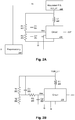
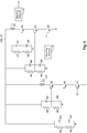
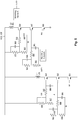
- the present disclosure includes an amplifier circuit comprising a first transistor having a control terminal, a first terminal, and a second terminal, the control terminal configured to receive an input signal, a cascode transistor having a control terminal, a first terminal, and a second terminal, wherein the second terminal of the cascode transistor is coupled to the first terminal of the first transistor, an inductor having a first terminal coupled to the first terminal of the cascode transistor and a second terminal coupled to a modulated power supply terminal, a first resistor having a first terminal coupled to the modulated power supply terminal and a second terminal coupled to a first node, a second resistor having a first terminal coupled to the first node and a second terminal coupled to a reference voltage, and a capacitor having a first terminal coupled to the modulated power supply terminal and a second terminal coupled to the first node, wherein the first node is coupled to the control terminal of the cascode transistor, and wherein the modulated power supply terminal produces a time varying power supply signal corresponding to the input signal.
- a capacitor (C1) 203 is added in parallel with the top resistor (R1) 201 of the resistor ladder to perform a zero-pole cancellation with the existing pole established by the bottom resistor ladder resistor (R2) 202 and a capacitance (C2) 204 resulting in a significant bandwidth extension.
- Capacitance C2 204 may be the total capacitance at the transistor bias node, for example, and may include intrinsic device capacitance, any further capacitance added to the node (e.g., MIM or MOS capacitances) as well as parasitic capacitances.
- the addition of capacitor C1 allows use of significantly larger values of resistors R1 and R2, which may result in a higher PAE, for example.
Landscapes
- Engineering & Computer Science (AREA)
- Power Engineering (AREA)
- Amplifiers (AREA)
Claims (14)
- Circuit amplificateur comprenant :un premier transistor (410) ayant une borne de commande, une première borne et une deuxième borne, la borne de commande étant agencée pour recevoir un signal d'entrée (IN1) ;un premier transistor cascode (412) ayant une borne de commande, une première borne agencée pour fournir un signal de sortie (OUT1), et une deuxième borne, la deuxième borne du transistor cascode étant couplée à la première borne du premier transistor ;une inductance (413) ayant une première borne couplée à la première borne du premier transistor cascode (412) et une deuxième borne couplée à une borne d'alimentation modulée ;un premier circuit de polarisation comprenant :une première résistance (405) ayant une première borne directement couplée à la borne d'alimentation modulée et une deuxième borne couplée à un premier nœud ;une deuxième résistance (406) ayant une première borne couplée au premier nœud et une deuxième borne couplée à une tension de référence ; etun premier condensateur (407) ayant une première borne directement couplée à la borne d'alimentation modulée et une deuxième borne couplée au premier nœud ;le circuit amplificateur comprenant en outre :
un deuxième transistor cascode (411) ayant une borne de commande, une première borne et une deuxième borne, dans lequel la première borne du deuxième transistor cascode est couplée à la deuxième borne du premier transistor cascode (412), et dans lequel la deuxième borne du deuxième transistor cascode est couplée à la première borne du premier transistor (410) ;un deuxième circuit de polarisation comprenant :une troisième résistance (401) ayant une première borne couplée directement à la borne d'alimentation modulée et une deuxième borne couplée à un deuxième nœud ;une quatrième résistance (402) ayant une première borne couplée au deuxième nœud et une deuxième borne couplée à la tension de référence ; etun deuxième condensateur (403) ayant une première borne directement couplée à la borne d'alimentation modulée et une deuxième borne couplée au deuxième nœud, etdans lequel le premier nœud est couplé à la borne de commande du premier transistor cascode, dans lequel le deuxième nœud est couplé à la borne de commande du deuxième transistor cascode (411), dans lequel la borne d'alimentation modulée est agencée pour fournir un signal d'alimentation variable dans le temps correspondant au signal d'entrée ; et dans lequel l'inductance (413) est agencée pour isoler la première borne du premier transistor cascode (412) par rapport au signal d'alimentation variable dans le temps sur la deuxième borne de l'inductance (413), et agencée pour isoler le premier circuit de polarisation du signal de sortie (OUT1). - Circuit selon la revendication 1, dans lequel la borne de commande du premier transistor cascode (412) comprend une capacité.
- Circuit selon la revendication 2, dans lequel la première résistance (405), la deuxième résistance (406) et le premier condensateur (407) sont agencés pour coupler le signal d'alimentation variable dans le temps à la borne de commande du premier transistor cascode (412) sur une première plage de fréquences plus grande qu'une deuxième plage de fréquences du signal d'entrée.
- Circuit selon la revendication 1, dans lequel un premier produit entre une résistance de la première résistance (405) et une capacité du premier condensateur (407) est approximativement égal à un deuxième produit entre une résistance de la deuxième résistance (406) et une capacité au niveau de la borne de commande du premier transistor cascode (412).
- Circuit selon la revendication 1, comprenant en outre une cinquième résistance couplée entre le premier nœud et la borne de commande du premier transistor cascode (412).
- Circuit selon la revendication 1, dans lequel la largeur de bande du signal d'entrée est inférieure à la largeur de bande du signal d'alimentation variable dans le temps.
- Circuit selon la revendication 1, dans lequel au moins l'un de la première résistance (405), de la deuxième résistance (406) et du premier condensateur (412) est programmable.
- Procédé d'amplification d'un signal comprenant :recevoir un signal d'entrée sur une borne de commande d'un premier transistor (410), le premier transistor ayant une borne de commande, une première borne et une deuxième borne ;coupler le signal d'entrée par l'intermédiaire du premier transistor et d'un premier transistor cascode (412) pour produire un signal de sortie sur une première borne du premier transistor cascode, le premier transistor cascode ayant une borne de commande, la première borne, et une deuxième borne, dans lequel la deuxième borne du premier transistor cascode est couplée à la première borne du premier transistor (410) ;recevoir une tension d'alimentation variable dans le temps à partir d'une alimentation modulée sur une borne d'un premier circuit de polarisation, le premier circuit de polarisation comprenant une première résistance (405) ayant une première borne couplée directement à la borne d'alimentation modulée et une deuxième borne couplée à un premier nœud, une deuxième résistance (406) ayant une première borne couplée au premier nœud et une deuxième borne couplée à une tension de référence, et un premier condensateur (407) ayant une première borne couplée directement à la borne d'alimentation modulée et une deuxième borne couplée au premier nœud, dans lequel le premier nœud est couplé à la borne de commande du premier transistor cascode (412) ;recevoir la tension d'alimentation variable dans le temps à partir de l'alimentation modulée sur une borne d'un deuxième circuit de polarisation, le deuxième circuit de polarisation comprenant une troisième résistance (401) ayant une première borne couplée directement à la borne d'alimentation modulée et une deuxième borne couplée à un deuxième nœud, une quatrième résistance (402) ayant une première borne couplée au deuxième nœud et une deuxième borne couplée à la tension de référence, et un deuxième condensateur (403) ayant une première borne couplée directement à la borne d'alimentation modulée et une deuxième borne couplée au deuxième nœud, dans lequel le deuxième nœud est couplé à une borne de commande du deuxième transistor cascode (411) ; etcoupler la tension d'alimentation variable dans le temps à la borne de commande du premier transistor cascode (412) ;coupler la tension d'alimentation variable dans le temps à la borne de commande du deuxième transistor cascode (411) ; etgénérer une impédance dans une inductance ayant une première borne couplée à la première borne du premier transistor cascode et une deuxième borne couplée à une borne d'alimentation modulée pour isoler la première borne du premier transistor cascode de la tension d'alimentation variable dans le temps, et pour isoler le premier circuit de polarisation du signal de sortie.
- Procédé selon la revendication 8, dans lequel la borne de commande du premier transistor cascode comprend une capacité.
- Procédé selon la revendication 9, dans lequel la première résistance (405), la deuxième résistance (406) et le premier condensateur (407) sont agencés pour coupler la tension d'alimentation variable dans le temps à la borne de commande du premier transistor cascode sur une première plage de fréquences plus grande qu'une deuxième plage de fréquences du signal d'entrée.
- Procédé selon la revendication 8, dans lequel un premier produit entre une résistance de la première résistance (405) et une capacité du premier condensateur (407) est sensiblement égal à un deuxième produit entre une résistance de la deuxième résistance (406) et une capacité de la borne de commande du premier transistor cascode (412).
- Procédé selon la revendication 8, comprenant en outre un couplage de la tension d'alimentation variable dans le temps par l'intermédiaire d'une cinquième résistance couplée entre le premier nœud et la borne de commande du premier transistor cascode (412).
- Procédé selon la revendication 8, dans lequel la largeur de bande du signal d'entrée est inférieure à la largeur de bande du signal d'alimentation variable dans le temps.
- Procédé selon la revendication 8, dans lequel au moins l'un de la première résistance (407), de la deuxième résistance (406) et du premier condensateur (404) est programmable.
Applications Claiming Priority (3)
| Application Number | Priority Date | Filing Date | Title |
|---|---|---|---|
| US201361876347P | 2013-09-11 | 2013-09-11 | |
| US14/172,150 US9219447B2 (en) | 2013-09-11 | 2014-02-04 | Wideband bias circuits and methods |
| PCT/US2014/055091 WO2015038712A1 (fr) | 2013-09-11 | 2014-09-11 | Procédés et circuits de polarisation à large bande |
Publications (2)
| Publication Number | Publication Date |
|---|---|
| EP3044871A1 EP3044871A1 (fr) | 2016-07-20 |
| EP3044871B1 true EP3044871B1 (fr) | 2020-05-06 |
Family
ID=52625027
Family Applications (1)
| Application Number | Title | Priority Date | Filing Date |
|---|---|---|---|
| EP14771491.9A Active EP3044871B1 (fr) | 2013-09-11 | 2014-09-11 | Procédés et circuits de polarisation à large bande |
Country Status (6)
| Country | Link |
|---|---|
| US (2) | US9219447B2 (fr) |
| EP (1) | EP3044871B1 (fr) |
| JP (1) | JP6567531B2 (fr) |
| KR (1) | KR20160056907A (fr) |
| CN (1) | CN105765858B (fr) |
| WO (1) | WO2015038712A1 (fr) |
Families Citing this family (13)
| Publication number | Priority date | Publication date | Assignee | Title |
|---|---|---|---|---|
| US9219447B2 (en) | 2013-09-11 | 2015-12-22 | Qualcomm Incorporated | Wideband bias circuits and methods |
| US9252713B2 (en) * | 2014-02-27 | 2016-02-02 | Qualcomm Incorporated | Bias circuits and methods for stacked devices |
| US9948252B1 (en) | 2017-04-06 | 2018-04-17 | Psemi Corporation | Device stack with novel gate capacitor topology |
| US10700643B2 (en) * | 2017-09-22 | 2020-06-30 | Qualcomm Incorporated | Envelope-shaped bias for power amplifier |
| US10291194B2 (en) * | 2017-10-09 | 2019-05-14 | Infineon Technologies Ag | System and method for biasing an RF circuit |
| TWI688203B (zh) * | 2017-12-14 | 2020-03-11 | 財團法人工業技術研究院 | 寬頻轉阻放大器電路 |
| WO2019114978A1 (fr) * | 2017-12-15 | 2019-06-20 | Huawei Technologies Co., Ltd. | Amplificateur cascode différentiel pour communication optique avec fréquence passe-bande accordable |
| JP7071860B2 (ja) | 2018-03-30 | 2022-05-19 | 株式会社村田製作所 | 増幅回路 |
| IT201800010793A1 (it) * | 2018-12-04 | 2020-06-04 | St Microelectronics Srl | Circuito di rilevazione, dispositivo e procedimento corrispondenti |
| CN114946122B (zh) * | 2020-01-20 | 2026-02-06 | 华为技术有限公司 | 堆叠放大器、射频收发电路、设备及切换控制方法 |
| US12113486B2 (en) * | 2020-11-20 | 2024-10-08 | The Boeing Company | Amplifier with stacked transconducting cells in parallel and/or cascade “current mode” combining |
| CN116094469B (zh) * | 2023-04-11 | 2023-06-30 | 南京米乐为微电子科技有限公司 | 一种共栅放大电路、低噪声放大器以及一种超宽带接收机 |
| WO2025110196A1 (fr) * | 2023-11-22 | 2025-05-30 | 株式会社村田製作所 | Circuit d'amplification de puissance |
Family Cites Families (13)
| Publication number | Priority date | Publication date | Assignee | Title |
|---|---|---|---|---|
| WO1981001924A1 (fr) * | 1979-12-28 | 1981-07-09 | Int Rectifier Corp Jp Ltd | Configuration de circuit de transistor a effet de champ |
| US6137367A (en) * | 1998-03-24 | 2000-10-24 | Amcom Communications, Inc. | High power high impedance microwave devices for power applications |
| JP4821214B2 (ja) * | 2005-08-26 | 2011-11-24 | 三菱電機株式会社 | カスコード接続回路 |
| US7355375B2 (en) | 2005-09-30 | 2008-04-08 | Nxp B.V. | Dynamic bias circuit for use with a stacked device arrangement |
| EP2220762B1 (fr) | 2007-11-09 | 2013-07-03 | ST-Ericsson SA (ST-Ericsson Ltd) | Circuit électronique avec amplificateur cascode |
| US8847689B2 (en) * | 2009-08-19 | 2014-09-30 | Qualcomm Incorporated | Stacked amplifier with diode-based biasing |
| KR101266918B1 (ko) * | 2009-09-14 | 2013-05-24 | 한국전자통신연구원 | 가변이득 광대역 피드백 저 잡음 증폭기 |
| US8111104B2 (en) | 2010-01-25 | 2012-02-07 | Peregrine Semiconductor Corporation | Biasing methods and devices for power amplifiers |
| US8120414B2 (en) | 2010-06-01 | 2012-02-21 | Enerdel, Inc. | Low-noise current source |
| US8427241B2 (en) * | 2011-05-24 | 2013-04-23 | Amcom Communications, Inc. | High efficiency, high frequency amplifiers |
| US8493154B1 (en) * | 2011-10-28 | 2013-07-23 | Berex Corporation | Linearity enhancement on cascode gain block amplifier |
| KR101767718B1 (ko) | 2011-11-04 | 2017-08-11 | 스카이워크스 솔루션즈, 인코포레이티드 | 전력 증폭기들에 대한 장치 및 방법 |
| US9219447B2 (en) | 2013-09-11 | 2015-12-22 | Qualcomm Incorporated | Wideband bias circuits and methods |
-
2014
- 2014-02-04 US US14/172,150 patent/US9219447B2/en active Active
- 2014-09-11 WO PCT/US2014/055091 patent/WO2015038712A1/fr not_active Ceased
- 2014-09-11 EP EP14771491.9A patent/EP3044871B1/fr active Active
- 2014-09-11 JP JP2016542085A patent/JP6567531B2/ja active Active
- 2014-09-11 KR KR1020167008943A patent/KR20160056907A/ko not_active Ceased
- 2014-09-11 CN CN201480049100.1A patent/CN105765858B/zh active Active
-
2015
- 2015-11-03 US US14/931,562 patent/US9467106B2/en not_active Expired - Fee Related
Non-Patent Citations (1)
| Title |
|---|
| None * |
Also Published As
| Publication number | Publication date |
|---|---|
| US20160056779A1 (en) | 2016-02-25 |
| US20150070095A1 (en) | 2015-03-12 |
| WO2015038712A1 (fr) | 2015-03-19 |
| US9219447B2 (en) | 2015-12-22 |
| US9467106B2 (en) | 2016-10-11 |
| JP6567531B2 (ja) | 2019-08-28 |
| CN105765858A (zh) | 2016-07-13 |
| JP2016530845A (ja) | 2016-09-29 |
| KR20160056907A (ko) | 2016-05-20 |
| EP3044871A1 (fr) | 2016-07-20 |
| CN105765858B (zh) | 2019-04-02 |
Similar Documents
| Publication | Publication Date | Title |
|---|---|---|
| EP3044871B1 (fr) | Procédés et circuits de polarisation à large bande | |
| KR102287445B1 (ko) | 저잡음 증폭기를 바이패스하는 시스템 및 방법 | |
| US10230340B1 (en) | Wide modulation bandwidth radio frequency circuit | |
| KR101113492B1 (ko) | 고전력 튜너블 캐패시터 | |
| US10224876B2 (en) | Low dropout voltage regulator for highly linear radio frequency power amplifiers | |
| US8594583B2 (en) | Apparatus and method for radio frequency reception with temperature and frequency independent gain | |
| US7937064B2 (en) | Wireless transceiver and method of operating the same | |
| CN101971512B (zh) | 隐性方向控制的射频发送接收器前端 | |
| US20200220503A1 (en) | Low noise amplifier and semiconductor device | |
| JP5743983B2 (ja) | 送受切替回路、無線装置および送受切替方法 | |
| US10566942B2 (en) | Active device which has a high breakdown voltage, is memory-less, traps even harmonic signals and circuits used therewith | |
| US12249960B2 (en) | Active balun design | |
| JP5807762B2 (ja) | 高周波モジュール及びそれを用いた携帯端末 | |
| GB2490977A (en) | A configurable LNA with inductive degeneration or with an impedance-matching stage in parallel with the principal gain stage | |
| US11405070B2 (en) | Radio transceivers | |
| Djugova et al. | Inverter-based low-noise amplifier topologies for ultra-wideband applications | |
| US20230018356A1 (en) | Amplifier for a radio frequency receiver | |
| WO2006095416A1 (fr) | Amplificateur haute frequence muni d'un attenuateur | |
| CN112803960B (zh) | 收发器装置 | |
| US20220294399A1 (en) | Semiconductor device | |
| EP3158642B1 (fr) | Dispositif actif sans mémoire qui piège les signaux d'harmoniques paires |
Legal Events
| Date | Code | Title | Description |
|---|---|---|---|
| PUAI | Public reference made under article 153(3) epc to a published international application that has entered the european phase |
Free format text: ORIGINAL CODE: 0009012 |
|
| 17P | Request for examination filed |
Effective date: 20160216 |
|
| AK | Designated contracting states |
Kind code of ref document: A1 Designated state(s): AL AT BE BG CH CY CZ DE DK EE ES FI FR GB GR HR HU IE IS IT LI LT LU LV MC MK MT NL NO PL PT RO RS SE SI SK SM TR |
|
| AX | Request for extension of the european patent |
Extension state: BA ME |
|
| DAX | Request for extension of the european patent (deleted) | ||
| STAA | Information on the status of an ep patent application or granted ep patent |
Free format text: STATUS: EXAMINATION IS IN PROGRESS |
|
| 17Q | First examination report despatched |
Effective date: 20190522 |
|
| GRAP | Despatch of communication of intention to grant a patent |
Free format text: ORIGINAL CODE: EPIDOSNIGR1 |
|
| STAA | Information on the status of an ep patent application or granted ep patent |
Free format text: STATUS: GRANT OF PATENT IS INTENDED |
|
| INTG | Intention to grant announced |
Effective date: 20191125 |
|
| GRAS | Grant fee paid |
Free format text: ORIGINAL CODE: EPIDOSNIGR3 |
|
| GRAA | (expected) grant |
Free format text: ORIGINAL CODE: 0009210 |
|
| STAA | Information on the status of an ep patent application or granted ep patent |
Free format text: STATUS: THE PATENT HAS BEEN GRANTED |
|
| AK | Designated contracting states |
Kind code of ref document: B1 Designated state(s): AL AT BE BG CH CY CZ DE DK EE ES FI FR GB GR HR HU IE IS IT LI LT LU LV MC MK MT NL NO PL PT RO RS SE SI SK SM TR |
|
| REG | Reference to a national code |
Ref country code: GB Ref legal event code: FG4D |
|
| REG | Reference to a national code |
Ref country code: CH Ref legal event code: EP Ref country code: AT Ref legal event code: REF Ref document number: 1268459 Country of ref document: AT Kind code of ref document: T Effective date: 20200515 |
|
| REG | Reference to a national code |
Ref country code: IE Ref legal event code: FG4D |
|
| REG | Reference to a national code |
Ref country code: DE Ref legal event code: R096 Ref document number: 602014065060 Country of ref document: DE |
|
| REG | Reference to a national code |
Ref country code: LT Ref legal event code: MG4D |
|
| REG | Reference to a national code |
Ref country code: NL Ref legal event code: MP Effective date: 20200506 |
|
| PG25 | Lapsed in a contracting state [announced via postgrant information from national office to epo] |
Ref country code: SE Free format text: LAPSE BECAUSE OF FAILURE TO SUBMIT A TRANSLATION OF THE DESCRIPTION OR TO PAY THE FEE WITHIN THE PRESCRIBED TIME-LIMIT Effective date: 20200506 Ref country code: NO Free format text: LAPSE BECAUSE OF FAILURE TO SUBMIT A TRANSLATION OF THE DESCRIPTION OR TO PAY THE FEE WITHIN THE PRESCRIBED TIME-LIMIT Effective date: 20200806 Ref country code: FI Free format text: LAPSE BECAUSE OF FAILURE TO SUBMIT A TRANSLATION OF THE DESCRIPTION OR TO PAY THE FEE WITHIN THE PRESCRIBED TIME-LIMIT Effective date: 20200506 Ref country code: PT Free format text: LAPSE BECAUSE OF FAILURE TO SUBMIT A TRANSLATION OF THE DESCRIPTION OR TO PAY THE FEE WITHIN THE PRESCRIBED TIME-LIMIT Effective date: 20200907 Ref country code: IS Free format text: LAPSE BECAUSE OF FAILURE TO SUBMIT A TRANSLATION OF THE DESCRIPTION OR TO PAY THE FEE WITHIN THE PRESCRIBED TIME-LIMIT Effective date: 20200906 Ref country code: GR Free format text: LAPSE BECAUSE OF FAILURE TO SUBMIT A TRANSLATION OF THE DESCRIPTION OR TO PAY THE FEE WITHIN THE PRESCRIBED TIME-LIMIT Effective date: 20200807 Ref country code: LT Free format text: LAPSE BECAUSE OF FAILURE TO SUBMIT A TRANSLATION OF THE DESCRIPTION OR TO PAY THE FEE WITHIN THE PRESCRIBED TIME-LIMIT Effective date: 20200506 |
|
| PG25 | Lapsed in a contracting state [announced via postgrant information from national office to epo] |
Ref country code: LV Free format text: LAPSE BECAUSE OF FAILURE TO SUBMIT A TRANSLATION OF THE DESCRIPTION OR TO PAY THE FEE WITHIN THE PRESCRIBED TIME-LIMIT Effective date: 20200506 Ref country code: HR Free format text: LAPSE BECAUSE OF FAILURE TO SUBMIT A TRANSLATION OF THE DESCRIPTION OR TO PAY THE FEE WITHIN THE PRESCRIBED TIME-LIMIT Effective date: 20200506 Ref country code: RS Free format text: LAPSE BECAUSE OF FAILURE TO SUBMIT A TRANSLATION OF THE DESCRIPTION OR TO PAY THE FEE WITHIN THE PRESCRIBED TIME-LIMIT Effective date: 20200506 Ref country code: BG Free format text: LAPSE BECAUSE OF FAILURE TO SUBMIT A TRANSLATION OF THE DESCRIPTION OR TO PAY THE FEE WITHIN THE PRESCRIBED TIME-LIMIT Effective date: 20200806 |
|
| REG | Reference to a national code |
Ref country code: AT Ref legal event code: MK05 Ref document number: 1268459 Country of ref document: AT Kind code of ref document: T Effective date: 20200506 |
|
| PG25 | Lapsed in a contracting state [announced via postgrant information from national office to epo] |
Ref country code: NL Free format text: LAPSE BECAUSE OF FAILURE TO SUBMIT A TRANSLATION OF THE DESCRIPTION OR TO PAY THE FEE WITHIN THE PRESCRIBED TIME-LIMIT Effective date: 20200506 Ref country code: AL Free format text: LAPSE BECAUSE OF FAILURE TO SUBMIT A TRANSLATION OF THE DESCRIPTION OR TO PAY THE FEE WITHIN THE PRESCRIBED TIME-LIMIT Effective date: 20200506 |
|
| PG25 | Lapsed in a contracting state [announced via postgrant information from national office to epo] |
Ref country code: CZ Free format text: LAPSE BECAUSE OF FAILURE TO SUBMIT A TRANSLATION OF THE DESCRIPTION OR TO PAY THE FEE WITHIN THE PRESCRIBED TIME-LIMIT Effective date: 20200506 Ref country code: RO Free format text: LAPSE BECAUSE OF FAILURE TO SUBMIT A TRANSLATION OF THE DESCRIPTION OR TO PAY THE FEE WITHIN THE PRESCRIBED TIME-LIMIT Effective date: 20200506 Ref country code: SM Free format text: LAPSE BECAUSE OF FAILURE TO SUBMIT A TRANSLATION OF THE DESCRIPTION OR TO PAY THE FEE WITHIN THE PRESCRIBED TIME-LIMIT Effective date: 20200506 Ref country code: IT Free format text: LAPSE BECAUSE OF FAILURE TO SUBMIT A TRANSLATION OF THE DESCRIPTION OR TO PAY THE FEE WITHIN THE PRESCRIBED TIME-LIMIT Effective date: 20200506 Ref country code: DK Free format text: LAPSE BECAUSE OF FAILURE TO SUBMIT A TRANSLATION OF THE DESCRIPTION OR TO PAY THE FEE WITHIN THE PRESCRIBED TIME-LIMIT Effective date: 20200506 Ref country code: AT Free format text: LAPSE BECAUSE OF FAILURE TO SUBMIT A TRANSLATION OF THE DESCRIPTION OR TO PAY THE FEE WITHIN THE PRESCRIBED TIME-LIMIT Effective date: 20200506 Ref country code: EE Free format text: LAPSE BECAUSE OF FAILURE TO SUBMIT A TRANSLATION OF THE DESCRIPTION OR TO PAY THE FEE WITHIN THE PRESCRIBED TIME-LIMIT Effective date: 20200506 Ref country code: ES Free format text: LAPSE BECAUSE OF FAILURE TO SUBMIT A TRANSLATION OF THE DESCRIPTION OR TO PAY THE FEE WITHIN THE PRESCRIBED TIME-LIMIT Effective date: 20200506 |
|
| REG | Reference to a national code |
Ref country code: DE Ref legal event code: R097 Ref document number: 602014065060 Country of ref document: DE |
|
| PG25 | Lapsed in a contracting state [announced via postgrant information from national office to epo] |
Ref country code: SK Free format text: LAPSE BECAUSE OF FAILURE TO SUBMIT A TRANSLATION OF THE DESCRIPTION OR TO PAY THE FEE WITHIN THE PRESCRIBED TIME-LIMIT Effective date: 20200506 Ref country code: PL Free format text: LAPSE BECAUSE OF FAILURE TO SUBMIT A TRANSLATION OF THE DESCRIPTION OR TO PAY THE FEE WITHIN THE PRESCRIBED TIME-LIMIT Effective date: 20200506 |
|
| PLBE | No opposition filed within time limit |
Free format text: ORIGINAL CODE: 0009261 |
|
| STAA | Information on the status of an ep patent application or granted ep patent |
Free format text: STATUS: NO OPPOSITION FILED WITHIN TIME LIMIT |
|
| REG | Reference to a national code |
Ref country code: DE Ref legal event code: R119 Ref document number: 602014065060 Country of ref document: DE |
|
| 26N | No opposition filed |
Effective date: 20210209 |
|
| PG25 | Lapsed in a contracting state [announced via postgrant information from national office to epo] |
Ref country code: MC Free format text: LAPSE BECAUSE OF FAILURE TO SUBMIT A TRANSLATION OF THE DESCRIPTION OR TO PAY THE FEE WITHIN THE PRESCRIBED TIME-LIMIT Effective date: 20200506 |
|
| REG | Reference to a national code |
Ref country code: CH Ref legal event code: PL |
|
| PG25 | Lapsed in a contracting state [announced via postgrant information from national office to epo] |
Ref country code: SI Free format text: LAPSE BECAUSE OF FAILURE TO SUBMIT A TRANSLATION OF THE DESCRIPTION OR TO PAY THE FEE WITHIN THE PRESCRIBED TIME-LIMIT Effective date: 20200506 |
|
| REG | Reference to a national code |
Ref country code: BE Ref legal event code: MM Effective date: 20200930 |
|
| PG25 | Lapsed in a contracting state [announced via postgrant information from national office to epo] |
Ref country code: LU Free format text: LAPSE BECAUSE OF NON-PAYMENT OF DUE FEES Effective date: 20200911 |
|
| PG25 | Lapsed in a contracting state [announced via postgrant information from national office to epo] |
Ref country code: DE Free format text: LAPSE BECAUSE OF NON-PAYMENT OF DUE FEES Effective date: 20210401 Ref country code: FR Free format text: LAPSE BECAUSE OF NON-PAYMENT OF DUE FEES Effective date: 20200930 |
|
| PG25 | Lapsed in a contracting state [announced via postgrant information from national office to epo] |
Ref country code: BE Free format text: LAPSE BECAUSE OF NON-PAYMENT OF DUE FEES Effective date: 20200930 Ref country code: CH Free format text: LAPSE BECAUSE OF NON-PAYMENT OF DUE FEES Effective date: 20200930 Ref country code: IE Free format text: LAPSE BECAUSE OF NON-PAYMENT OF DUE FEES Effective date: 20200911 Ref country code: LI Free format text: LAPSE BECAUSE OF NON-PAYMENT OF DUE FEES Effective date: 20200930 |
|
| PG25 | Lapsed in a contracting state [announced via postgrant information from national office to epo] |
Ref country code: TR Free format text: LAPSE BECAUSE OF FAILURE TO SUBMIT A TRANSLATION OF THE DESCRIPTION OR TO PAY THE FEE WITHIN THE PRESCRIBED TIME-LIMIT Effective date: 20200506 Ref country code: MT Free format text: LAPSE BECAUSE OF FAILURE TO SUBMIT A TRANSLATION OF THE DESCRIPTION OR TO PAY THE FEE WITHIN THE PRESCRIBED TIME-LIMIT Effective date: 20200506 Ref country code: CY Free format text: LAPSE BECAUSE OF FAILURE TO SUBMIT A TRANSLATION OF THE DESCRIPTION OR TO PAY THE FEE WITHIN THE PRESCRIBED TIME-LIMIT Effective date: 20200506 |
|
| PG25 | Lapsed in a contracting state [announced via postgrant information from national office to epo] |
Ref country code: MK Free format text: LAPSE BECAUSE OF FAILURE TO SUBMIT A TRANSLATION OF THE DESCRIPTION OR TO PAY THE FEE WITHIN THE PRESCRIBED TIME-LIMIT Effective date: 20200506 |
|
| PGFP | Annual fee paid to national office [announced via postgrant information from national office to epo] |
Ref country code: GB Payment date: 20240808 Year of fee payment: 11 |