EP3092573B1 - Methods for setting the address of a module - Google Patents
Methods for setting the address of a module Download PDFInfo
- Publication number
- EP3092573B1 EP3092573B1 EP15801525.5A EP15801525A EP3092573B1 EP 3092573 B1 EP3092573 B1 EP 3092573B1 EP 15801525 A EP15801525 A EP 15801525A EP 3092573 B1 EP3092573 B1 EP 3092573B1
- Authority
- EP
- European Patent Office
- Prior art keywords
- module
- address
- communication
- connection
- communication address
- Prior art date
- Legal status (The legal status is an assumption and is not a legal conclusion. Google has not performed a legal analysis and makes no representation as to the accuracy of the status listed.)
- Not-in-force
Links
Images



Classifications
-
- G—PHYSICS
- G06—COMPUTING OR CALCULATING; COUNTING
- G06F—ELECTRIC DIGITAL DATA PROCESSING
- G06F13/00—Interconnection of, or transfer of information or other signals between, memories, input/output devices or central processing units
- G06F13/38—Information transfer, e.g. on bus
- G06F13/40—Bus structure
- G06F13/4063—Device-to-bus coupling
- G06F13/4068—Electrical coupling
-
- G—PHYSICS
- G06—COMPUTING OR CALCULATING; COUNTING
- G06F—ELECTRIC DIGITAL DATA PROCESSING
- G06F13/00—Interconnection of, or transfer of information or other signals between, memories, input/output devices or central processing units
- G06F13/38—Information transfer, e.g. on bus
- G06F13/42—Bus transfer protocol, e.g. handshake; Synchronisation
- G06F13/4282—Bus transfer protocol, e.g. handshake; Synchronisation on a serial bus, e.g. I2C bus, SPI bus
- G06F13/4291—Bus transfer protocol, e.g. handshake; Synchronisation on a serial bus, e.g. I2C bus, SPI bus using a clocked protocol
-
- G—PHYSICS
- G06—COMPUTING OR CALCULATING; COUNTING
- G06F—ELECTRIC DIGITAL DATA PROCESSING
- G06F21/00—Security arrangements for protecting computers, components thereof, programs or data against unauthorised activity
- G06F21/70—Protecting specific internal or peripheral components, in which the protection of a component leads to protection of the entire computer
- G06F21/71—Protecting specific internal or peripheral components, in which the protection of a component leads to protection of the entire computer to assure secure computing or processing of information
- G06F21/73—Protecting specific internal or peripheral components, in which the protection of a component leads to protection of the entire computer to assure secure computing or processing of information by creating or determining hardware identification, e.g. serial numbers
-
- H—ELECTRICITY
- H04—ELECTRIC COMMUNICATION TECHNIQUE
- H04L—TRANSMISSION OF DIGITAL INFORMATION, e.g. TELEGRAPHIC COMMUNICATION
- H04L61/00—Network arrangements, protocols or services for addressing or naming
- H04L61/50—Address allocation
- H04L61/5038—Address allocation for local use, e.g. in LAN or USB networks, or in a controller area network [CAN]
Definitions
- the present disclosure relates generally to slave devices on a communication bus and more particularly to slave modules on an 12C bus.
- I 2 C 12C (also known as I 2 C) is an inter-device communication standard.
- An I2C bus has one master device and one or more slave devices. Each slave device has a unique communication address so that the master device can direct communication to a particular slave device.
- Printers have user-replaceable supply items such as toner bottles. These supply items may have authentication circuits to distinguish original equipment manufactured toner bottles from third-party toner bottles, since different operating procedures may apply. Authentication circuits may implement cryptography algorithms to increase confidence in the authentication.
- a single color printer such as a mono printer, may have an authentication circuit on a toner bottle and another authentication circuit on an imaging unit.
- These modules that contain the authentication circuits may be nearly identical, the only difference being a non-volatile memory variable that contains the module address. During manufacturing, extra expense must be expended to keep track of these two similar, but non-identical, modules, and the system will not operate correctly if the modules are mixed up. What is needed is a way to use identical modules on multiple supply items.
- US2013/0268231 relates to a sensor system in which wire-connected sensor modules can be identified individually without fixing the connecting positions of the sensor modules.
- the invention in one form thereof, is directed to a method of operating a module.
- the module has a power connection, a ground connection to which module voltages are referenced, and a serial communication connection.
- the method includes adjusting an impedance between the power connection and the ground connection to regulate a power connection voltage targeted to a predetermined target voltage, and setting a module communication address based on the adjustment.
- the invention in another form thereof, is directed to a method of operating a module that has a power connection and a ground connection.
- the method includes increasing current flowing into the module through the power connection to regulate a voltage between the power connection and the ground connection, and setting a module communication address based on the amount of current flowing into the module through the power connection.
- the invention in yet another form thereof, is directed to a method of operating a module.
- the module has a power connection, a ground connection, and a communication address.
- the method includes determining whether or not a voltage between the power connection and the ground connection is greater than a first predetermined threshold, and if so determined then decreasing an impedance between the power connection and the ground connection and setting the communication address to a first address.
- the method also includes determining whether or not the voltage between the power connection and the ground connection is less than a second predetermined threshold, and if so determined then increasing the impedance between the power connection and the ground connection and setting the communication address to a second address.
- the first address is not the same as the second address.
- a printer module network 100 has a system application specific integrated circuit (ASIC) 102 coupled to a first module 104 and to a second module 106 via an I2C bus.
- the I2C bus has a clock line 108 driven by the system ASIC 102 and a data line 110 driven bidirectionally by the system ASIC 102, the first module 104, and the second module 106.
- the clock line and the data line are serial communication connections.
- the system ASIC 102 is located on a system printed circuit board (PCB) 103.
- the first module 104 is located on a user-replaceable component, e.g., as shown a toner bottle 105.
- the first module 104 includes a PCB.
- a power connection 112, a ground connection 114, a clock connection 116, and a data connection 118 are, for example, conductive pads located on the first-module PCB. Compliant metal fingers touch the conductive pads forming electrical connections between the system PCB and the first module 104.
- power connection 112, ground connection 114, clock connection 116, and data connection 118 may be made with other reusable connections such as pin-in-socket connectors.
- the second module 106 has similar connections and is located on, for example, as shown an imaging unit 119.
- the system ASIC 102 is an I2C master, the first module 104 and the second module 106 are I2C slaves.
- a serial communication in the I2C data format contains a header that has a slave address.
- Each slave will only respond to communications that are addressed to its communication address.
- each slave on the I2C bus has a unique communication address.
- the communication address of the first module 104 is not fixed. Instead, the communication address is controlled by a first power voltage 120 and a first source resistor 122 located on the system PCB.
- the voltage between the power connection 112 and the ground connection 114, hereafter referred to as Vin, is regulated by the first module 104 using a shunt regulator 121, e.g., a zener diode.
- the communication address of the first module 104 is based on the amount of current flowing into the power connection 112, hereafter referred to as Iin.
- the communication address of the first module 104 may be based on, for example, an impedance between the power connection 112 and the ground connection 114, since this impedance will also influence Iin.
- Vin is regulated to a voltage
- Iin is controlled by the first power voltage 120 and the first source resistor 122.
- a second power voltage 124 is coupled to the second module 106 via a second source resistor 126.
- the second module 106 has a shunt regulator 123 coupled to Vin and ground, If, for example, the first module 104 is identical to the second module 106, the first power voltage 120 is the same as the second power voltage 124, and the first source resistor 122 is the same as the second source resistor 126, then the first module 104 and the second module 106 will have the same communication address which is unwanted as it will cause bus conflicts. However, if the first source resistor 122 is not the same as the second source resistor 126, then the first module 104 and the second module 106 will not have the same communication address since they will have different input currents, hereafter referred to as Iin.
- the first module 104 and the second module 106 are identical and will have a first communication address if Iin is greater than 40mA and a second communication address if Iin is less than 40mA.
- first power voltage 120 is 12V
- second power voltage 124 is 8V
- the first source resistor 122 is 100 ohms
- the second source resistor 126 is 65 ohms
- Vin is regulated to 6V
- the first-module I in is 60mA and the second-module Iin is 30mA, and thus the communication address of the two modules will be different.
- the disclosed system has two identical modules on the same I2C bus but at different addresses, and thisfunction is provided without adding additional connections. This allows the same module to be populated into multiple system components which simplifies manufacturing and lowers cost.
- USB universal serial bus
- a universal serial bus (USB) system also has slave devices with unique communication addresses. Instead of setting one of only two addresses, more addresses may be set by dividing Iin into more than two regions. For example, four addresses would be advantageous for toner bottles of a four color printer.
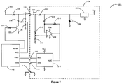
- FIG. 2 shows a schematic diagram depiction of the printer module network 100 showing internal details of the first module 104.
- Vin 202 downstream of power connection 112, is regulated by a zener diode 204 configured as a shunt regulator.
- the zener diode 204 is coupled to the power connection 112 via a sense resistor 206, which is sized so that it does not significantly degrade the ability of zener diode 204 to regulate Vin 202.
- Example component values are the Zener diode 204 is a 6V zener diode, sense resistor 206 is 1 ohm, and source resistor 122 is 100 ohms.
- the voltage across sense resistor 206 is proportional to the amount of current flowing into the first module 104 through the power connection 112 i.e. Iin.
- a differential amplifier made up of an op-amp 208 and resistors 210, 212, 214, 216, converts this differential voltage to a single-ended voltage referenced to ground. This single-ended voltage is coupled to an analog- to-digital converter (ADC) located in an authentication circuit 218.
- ADC analog- to-digital converter
- Authentication circuit 218 is a digital logic circuit and contains an I2C slave which is coupled to the system ASIC 102 via clock connection 116 and data connection 118. Note that the current through resistors 210, 212, 214, and 216 and the op-amp 208 is negligible compared to the current through sense resistor 206 and so does not add significant error to the measurement of Iin.
- Authentication circuit 218 has a communication address because it is an I2C slave device.
- I2C communication addresses are either 7 bits or 10 bits in length. The most significant bits are set, for example, to a value stored in non-volatile memory located within the authentication circuit 218. The least significant bit is set based on the voltage read by the ADC, which is proportional to Iin. If Iin is greater than a predetermined input current threshold, for example, 40 mA, the least significant bit of the first-module communication address is set to one, otherwise it is set to zero. Thus, the first-module communication address may be changed by changing the value of the source resistor 122 since the source resistor 122 influences Iin. The authentication circuit 218 responds to communications addressed to the communication address.
- the first-module communication address may also be changed by switching a ballast resistor 219 to ground.
- the ballast resistor 219 is, for example, 200 ohms. This will reduce the Thevenin equivalent voltage seen by the power connection 112 which will reduce Iin.
- the system ASIC 102 may switch in the ballast resistor 219 by turning on a transistor 220 via a resistor 222. In this way, the system ASIC 102 may dynamically change the first- module communication address to verify, for example, that the first module 104 is operating correctly.
- the system ASIC 102 may verify that the first module 104 is regulating Vin by reading an ADC coupled to Vin via resistor 224 and resistor 226.
- the authentication circuit 218 may behave erratically if its power voltage droops, which may happen if the zener diode 204 fails to regulate Vin.
- Authentication circuit Vcc is supplied by a linear regulator 228. Alternatively, the authentication circuit 218 may be supplied by Vin and the linear regulator may be omitted.
- FIG. 3 shows a schematic diagram depiction of a module 300 according to another embodiment of the present disclosure.
- the module 300 has the same electrical interface as the first module 104.
- a sense resistor 316 activates a transistor 318 when Iin exceeds a predetermined threshold Ith, e.g., 40mA.
- Transistor 318 is coupled to a digital circuit 320 via a voltage divider made of resistor 322 and resistor 324.
- the digital circuit 320 is, for example, a non-volatile memory, e.g., EEPROM, flash, etc.
- the digital circuit 320 is an I2C slave, and its communication address is based on the state of the address line 326. The communication address will be a first address when lin is below Ith and will be a second address when
- FIG. 4 shows a schematic diagram depiction of a module 400 according to another embodiment of the present disclosure.
- the module 400 has the same electrical interface as the first module 104.
- the output of the op-amp 402 is a control line 413 that adjusts the current in the adjustable current sink since the current through resistor 412 is inversely proportional to the voltage at the control line 413.
- the module 400 does not measure Iin directly. Instead, the control line 413 is coupled via resistor 414 and resistor 416 to an ADC in an authentication ASIC 418.
- the authentication ASIC 418 is a digital circuit that contains an authentication circuit.
- Vc1 the current through resistor 412 which is inversely proportional to the voltage on control line 413 hereinafter referred to as Vc1
- the authentication ASIC 418 reads Vc1 and sets a communication address based on this voltage. For example, the communication address may be set to a first address when Vcl exceeds a predetermined threshold and may otherwise be set to a second address. Of course, more communication addresses are possible with multiple thresholds.
- the authentication ASIC 418 responds to communications addressed to the communication address.
- the authentication ASIC 418 may synchronize setting the communication address to when the authentication circuit is in a low-power state, such as, for example, when the authentication circuit is in an idle state. This will reduce the current into the linear regulator 228 so that it is negligible.
- FIG. 5 shows a schematic diagram depiction of a printer module network 500.
- a module 502 is coupled to the system ASIC 102.
- the module 502 has the same electrical interface as the first module 104.
- Vin is coupled to an ADC input of a digital circuit 504 though resistor 506 and resistor 508.
- a digital output of the digital circuit 504 is coupled to a transistor 506 via a resistor 508.
- the transistor 506 is coupled to a resistor 510 that is coupled to Vin.
- the digital circuit 504 is an I2C slave device that has a communication address.
- the digital circuit 504 has a controller that controls Dout and sets the communication address based on the voltage at the ADC input, which is proportional to Vin. If Vin is greater than a first predetermined threshold, the controller turns on Dout which decreases the impedance between a power connection 112 and a ground connection 114 and sets the communication address to a first address. If Vin is less than a second predetermined threshold, the controller turns off Dout which increases the impedance between the power connection 112 and the ground connection 114 and sets the communication address to a second address. If neither of these conditions are true then the controller does not change the state of Dout and does not change the communication address. The first address is not the same as the second address. The least significant bit of the communication address may be the same as Dout, and the most significant bits may be retrieved from NVRAM located in the digital circuit 504. The controller responds to communications addressed to the communication address.
- the first power voltage 120 is 12V
- the first source resistor 122 is 100 ohms
- resistor 218 is 200 ohms
- resistor 224 is 40k ohms
- resistor 226 is 10k ohms
- resistor 506 is 40k ohms
- resistor 508 is 10k ohms
- resistor 510 is 200 ohms
- the current into the linear regulator 228 negligible
- Vin 12V.
- the controller will determine that Vin is too high and will drive Dout high which will bring Vin down to 8V.
- the controller will determine that Vin is too low and will drive Dout low which will make Vin 8V. In this way, the module 502 regulates Vin.
- the first predetermined threshold is greater than the second predetermined threshold. This gives the system some hysteresis which makes the module more resistant to noise on Vin.
- the first predetermined threshold may be the same as the second predetermined threshold which may be cheaper to implement if, for example, the ADC is replaced by a comparator.
- the I2C slave device and the controller are integrated into the digital circuit which is an ASIC.
- the I2C slave device and the controller may be separate devices.
- the I2C slave device may include an authentication circuit.
- FIG. 6 shows a schematic diagram depiction of a module 600 according to another embodiment of the present disclosure.
- the module 600 has the same electrical interface as the first module 104.
- a shunt regulator 601 in ASIC 602 regulates Vin to a predetermined target voltage by adjusting an active current sink located within the shunt regulator 601.
- the ASIC 602 also has a current measuring circuit that measures the voltage across a resistor 604. The current sunk by shunt regulator 601 passes through the resistor 604.
- the ASIC 602 has a comparator that drives a digital output Dout based on the output of the current measuring circuit.
- the digital output Dout is coupled to an address input of a digital logic circuit 606 which is an I2C slave device.
- a communication address of the digital logic circuit 606 is based on the state of the address input.
- the digital logic circuit may include an authentication circuit.
- the module is configured to perform one or more of the methods disclosed below.
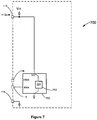
- FIG. 7 shows a schematic diagram depiction of a module 700 according to another embodiment of the present disclosure.
- the module 700 has the same electrical interface as the first module 104.
- An authentication ASIC 702 has a shunt regulator 703 that regulates Vin to a predetermined target voltage by adjusting an adjustable current sink located within shunt regulator 703.
- Shunt regulator 703 has a control line that adjusts the current sunk by the adjustable current sink.
- the authentication ASIC 702 is an I2C slave device with a communication address. The communication address is based on the stale of the control line.
- the authentication ASIC 702 may have a current measuring circuit that measures Iin and the communication address is based on the current measured.
- the module is configured to perform one or more of the methods disclosed below.
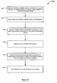
- FIG. 8 shows an example embodiment of a method of operating a module according to one embodiment
- Method 800 sets a module communication address based on an adjustment in impedance made to regulate a power connection voltage, which is influenced by the source voltage and source impedance supplied to the module. This enables identical modules to be coupled to the same communication bus at different addresses.
- the module has a power connection, a ground connection, a clock connection, and a data connection.
- the clock connection and the data connection are serial communication connections e.g. I2C.
- an impedance between the power connection and the ground connection is adjusted to regulate a power connection voltage targeted to a predetermined target voltage.
- the power connection voltage may be regulated to 6V.
- the regulation may have a tolerance, for example +/- 10% of the target voltage, depending on component tolerances and load variations,
- a module communication address is set based on the adjustment made at block 802. For example, if the adjusting included switching on a transistor connected to a ballast resistor to maintain regulation then the module communication address is set to a first address, Otherwise, the module communication address is set to a second address.
- more than two addresses may be used if the system has the capability to make finer adjustments of the impedance between the power connection and the ground connection.
- a first serial communication addressed to the module communication address is received.
- the serial communication connection may be, for example, the data connection.
- the first serial communication is responded to since it was addressed to the module communication address.
- an I2C serial communication may be a header containing a start condition, a read command, and a I2C slave address, formatted in the I2C data format. The response may be made by driving data on the data connection.
- a second serial communication is received addressed to a different address than the module communication address.
- the method 800 may repeat adjusting the impedance and setting the module communication address in response to changes in the source voltage or the source impedance.
- the module communication address may be changed dynamically to avoid a conflict if, for example, a new module is added to the I2C bus.
- the module may contain an authentication circuit used to verify the origin of the module.
- the authentication circuit may require a large amount of input current while it is performing an authentication.
- the method 800 may synchronize setting the module communication address to when the authentication circuit is in a lower-power state, such as an idle state, so that the current demands of the authentication circuit does not disturb the regulation of the power connection voltage,
- a lower-power state such as an idle state
- Other lower-power states may include, for example, memory reads, memory writes, etc.
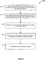
- Figure 9 shows an example embodiment of a method 900 of operating a module according to one embodiment.
- the module has a power connection, a ground connection, and a module communication address.
- the module communication address is set based on the amount of current flowing into the module through the power connection.
- the communication address may be set to one of two addresses. Alternatively, the communication address may be set to one of three or more addresses.
- a first communication addressed to the module communication address is responded to.
- the first communication may be formatted in the I2C data format.
- a second communication addressed to a different address than the module communication address is received.
- the module may have an authentication circuit.
- the method 900 may synchronize setting the module communication address to when the authentication circuit is in a lower-power state, such as an idle state.
- Figure 10 shows an example embodiment of a method 1000 of operating a module according to one embodiment.
- the module has a power connection, a ground connection, and a communication address.
- At block 1002 determine whether or not a voltage between the power connection and the ground connection is greater than a first predetermined threshold. If so determined, then at block 1004 decrease an impedance between the power connection and the ground connection, and at block 1006 set the communication address to a first address.
- the first address is not the same as the second address.
- the first predetermined threshold may be greater than the second predetermined threshold to provide hysteresis. Alternatively, the first predetermined threshold may be the same as the second predetermined threshold to simplify the determining act.
- the communication may be, for example, in the I2C data format.
- an ADC may be replaced by a comparator or a group of comparators.
- the acts of a method may be performed by a single controller, Alternatively, a plurality of circuits may perform one or more acts of a method. The acts of the methods may be performed in different orders than the given examples.
Landscapes
- Engineering & Computer Science (AREA)
- Theoretical Computer Science (AREA)
- General Engineering & Computer Science (AREA)
- Physics & Mathematics (AREA)
- General Physics & Mathematics (AREA)
- Computer Hardware Design (AREA)
- Computer Networks & Wireless Communication (AREA)
- Signal Processing (AREA)
- Mathematical Physics (AREA)
- Computer Security & Cryptography (AREA)
- Software Systems (AREA)
- Dc Digital Transmission (AREA)
- Cable Transmission Systems, Equalization Of Radio And Reduction Of Echo (AREA)
- Remote Monitoring And Control Of Power-Distribution Networks (AREA)
Description
- The present disclosure relates generally to slave devices on a communication bus and more particularly to slave modules on an 12C bus.
- 12C (also known as I2C) is an inter-device communication standard. An I2C bus has one master device and one or more slave devices. Each slave device has a unique communication address so that the master device can direct communication to a particular slave device.
- Printers have user-replaceable supply items such as toner bottles. These supply items may have authentication circuits to distinguish original equipment manufactured toner bottles from third-party toner bottles, since different operating procedures may apply. Authentication circuits may implement cryptography algorithms to increase confidence in the authentication. A single color printer, such as a mono printer, may have an authentication circuit on a toner bottle and another authentication circuit on an imaging unit. These modules that contain the authentication circuits may be nearly identical, the only difference being a non-volatile memory variable that contains the module address. During manufacturing, extra expense must be expended to keep track of these two similar, but non-identical, modules, and the system will not operate correctly if the modules are mixed up. What is needed is a way to use identical modules on multiple supply items.
US2013/0268231 relates to a sensor system in which wire-connected sensor modules can be identified individually without fixing the connecting positions of the sensor modules. - The invention, in one form thereof, is directed to a method of operating a module. The module has a power connection, a ground connection to which module voltages are referenced, and a serial communication connection. The method includes adjusting an impedance between the power connection and the ground connection to regulate a power connection voltage targeted to a predetermined target voltage, and setting a module communication address based on the adjustment.
- The invention, in another form thereof, is directed to a method of operating a module that has a power connection and a ground connection. The method includes increasing current flowing into the module through the power connection to regulate a voltage between the power connection and the ground connection, and setting a module communication address based on the amount of current flowing into the module through the power connection.
- The invention, in yet another form thereof, is directed to a method of operating a module. The module has a power connection, a ground connection, and a communication address. The method includes determining whether or not a voltage between the power connection and the ground connection is greater than a first predetermined threshold, and if so determined then decreasing an impedance between the power connection and the ground connection and setting the communication address to a first address. The method also includes determining whether or not the voltage between the power connection and the ground connection is less than a second predetermined threshold, and if so determined then increasing the impedance between the power connection and the ground connection and setting the communication address to a second address. The first address is not the same as the second address.
- The accompanying drawings incorporated in and forming a part of the specification, illustrate several aspects of the present disclosure, and together with the description serve to explain the principles of the present disclosure.
-
Figure 1 is a schematic diagram depiction of a printer module network according to one embodiment of the present disclosure. -
Figure 2 is a schematic diagram depiction showing internal details of the printer module network. -
Figures 3 - 7 are schematic diagram depictions of alternate embodiments of the printer module network -
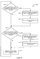
Figures 8 - 10 are flowcharts of methods of operating a module according to embodiments of the present disclosure. - In the following description, reference is made to the accompanying drawings where like numerals represent like elements. The embodiments are described in sufficient detail to enable those skilled in the art to practice the present disclosure. It is to be understood that other embodiments may be utilized and that process, electrical, and mechanical changes, etc., may be made without departing from the scope of the present disclosure. Examples merely typify possible variations. Portions and features of some embodiments may be included in or substituted for those of others. The following description, therefore, is not to be taken in a limiting sense and the scope of the present disclosure is defined only by the appended claims.
- Referring now to the drawings and more particularly to
Figure 1 , there is shown a schematic diagram depiction of a circuit according to one embodiment of the present disclosure. Aprinter module network 100 has a system application specific integrated circuit (ASIC) 102 coupled to afirst module 104 and to asecond module 106 via an I2C bus. The I2C bus has aclock line 108 driven by the system ASIC 102 and adata line 110 driven bidirectionally by the system ASIC 102, thefirst module 104, and thesecond module 106. The clock line and the data line are serial communication connections. - The system ASIC 102 is located on a system printed circuit board (PCB) 103. The
first module 104 is located on a user-replaceable component, e.g., as shown atoner bottle 105. Thefirst module 104 includes a PCB. Apower connection 112, aground connection 114, aclock connection 116, and adata connection 118 are, for example, conductive pads located on the first-module PCB. Compliant metal fingers touch the conductive pads forming electrical connections between the system PCB and thefirst module 104. Alternatively,power connection 112,ground connection 114,clock connection 116, anddata connection 118 may be made with other reusable connections such as pin-in-socket connectors. Thesecond module 106 has similar connections and is located on, for example, as shown animaging unit 119. - The system ASIC 102 is an I2C master, the
first module 104 and thesecond module 106 are I2C slaves. As is known in the art, a serial communication in the I2C data format contains a header that has a slave address. Each slave will only respond to communications that are addressed to its communication address. Thus, each slave on the I2C bus has a unique communication address. - The communication address of the
first module 104 is not fixed. Instead, the communication address is controlled by afirst power voltage 120 and afirst source resistor 122 located on the system PCB. The voltage between thepower connection 112 and theground connection 114, hereafter referred to as Vin, is regulated by thefirst module 104 using ashunt regulator 121, e.g., a zener diode. The communication address of thefirst module 104 is based on the amount of current flowing into thepower connection 112, hereafter referred to as Iin. Similarly, the communication address of thefirst module 104 may be based on, for example, an impedance between thepower connection 112 and theground connection 114, since this impedance will also influence Iin. Thus, when Vin is regulated to a voltage, Iin is controlled by thefirst power voltage 120 and thefirst source resistor 122. - A
second power voltage 124 is coupled to thesecond module 106 via asecond source resistor 126. Thesecond module 106 has ashunt regulator 123 coupled to Vin and ground, If, for example, thefirst module 104 is identical to thesecond module 106, thefirst power voltage 120 is the same as thesecond power voltage 124, and thefirst source resistor 122 is the same as thesecond source resistor 126, then thefirst module 104 and thesecond module 106 will have the same communication address which is unwanted as it will cause bus conflicts. However, if thefirst source resistor 122 is not the same as thesecond source resistor 126, then thefirst module 104 and thesecond module 106 will not have the same communication address since they will have different input currents, hereafter referred to as Iin. For example, thefirst module 104 and thesecond module 106 are identical and will have a first communication address if Iin is greater than 40mA and a second communication address if Iin is less than 40mA. Of course, other combinations of source resistor and power voltage will result in different Iin and thus different communication addresses. For example, if thefirst power voltage 120 is 12V, thesecond power voltage 124 is 8V, thefirst source resistor 122 is 100 ohms, thesecond source resistor 126 is 65 ohms, and Vin is regulated to 6V, then the first-module I in is 60mA and the second-module Iin is 30mA, and thus the communication address of the two modules will be different. - Note that the disclosed system has two identical modules on the same I2C bus but at different addresses, and thisfunction is provided without adding additional connections. This allows the same module to be populated into multiple system components which simplifies manufacturing and lowers cost.
- Note that other communication systems may be used instead of I2C. For example, a universal serial bus (USB) system also has slave devices with unique communication addresses. Instead of setting one of only two addresses, more addresses may be set by dividing Iin into more than two regions. For example, four addresses would be advantageous for toner bottles of a four color printer.
-
Figure 2 shows a schematic diagram depiction of theprinter module network 100 showing internal details of thefirst module 104.Vin 202, downstream ofpower connection 112, is regulated by azener diode 204 configured as a shunt regulator. Thezener diode 204 is coupled to thepower connection 112 via asense resistor 206, which is sized so that it does not significantly degrade the ability ofzener diode 204 to regulateVin 202. Example component values are theZener diode 204 is a 6V zener diode,sense resistor 206 is 1 ohm, andsource resistor 122 is 100 ohms. - The voltage across
sense resistor 206 is proportional to the amount of current flowing into thefirst module 104 through thepower connection 112 i.e. Iin. A differential amplifier, made up of an op-amp 208 andresistors authentication circuit 218.Authentication circuit 218 is a digital logic circuit and contains an I2C slave which is coupled to thesystem ASIC 102 viaclock connection 116 anddata connection 118. Note that the current throughresistors amp 208 is negligible compared to the current throughsense resistor 206 and so does not add significant error to the measurement of Iin. -
Authentication circuit 218 has a communication address because it is an I2C slave device. I2C communication addresses are either 7 bits or 10 bits in length. The most significant bits are set, for example, to a value stored in non-volatile memory located within theauthentication circuit 218. The least significant bit is set based on the voltage read by the ADC, which is proportional to Iin. If Iin is greater than a predetermined input current threshold, for example, 40 mA, the least significant bit of the first-module communication address is set to one, otherwise it is set to zero. Thus, the first-module communication address may be changed by changing the value of thesource resistor 122 since thesource resistor 122 influences Iin. Theauthentication circuit 218 responds to communications addressed to the communication address. - The first-module communication address may also be changed by switching a
ballast resistor 219 to ground. Theballast resistor 219 is, for example, 200 ohms. This will reduce the Thevenin equivalent voltage seen by thepower connection 112 which will reduce Iin. Thesystem ASIC 102 may switch in theballast resistor 219 by turning on atransistor 220 via aresistor 222. In this way, thesystem ASIC 102 may dynamically change the first- module communication address to verify, for example, that thefirst module 104 is operating correctly. - The
system ASIC 102 may verify that thefirst module 104 is regulating Vin by reading an ADC coupled to Vin viaresistor 224 andresistor 226. Theauthentication circuit 218 may behave erratically if its power voltage droops, which may happen if thezener diode 204 fails to regulate Vin. Authentication circuit Vcc is supplied by alinear regulator 228. Alternatively, theauthentication circuit 218 may be supplied by Vin and the linear regulator may be omitted. -
Figure 3 shows a schematic diagram depiction of amodule 300 according to another embodiment of the present disclosure. Themodule 300 has the same electrical interface as thefirst module 104. An op-amp 304, and associated components 306-314, forms an active current sink configured as a shunt regulator which regulates Vin to a predetermined target voltage e.g.6V. Asense resistor 316 activates atransistor 318 when Iin exceeds a predetermined threshold Ith, e.g., 40mA.Transistor 318 is coupled to adigital circuit 320 via a voltage divider made ofresistor 322 andresistor 324. Thedigital circuit 320 is, for example, a non-volatile memory, e.g., EEPROM, flash, etc. Thedigital circuit 320 is an I2C slave, and its communication address is based on the state of theaddress line 326.
The communication address will be a first address when lin is below Ith and will be a second address when Iin is above Ith. -
Figure 4 shows a schematic diagram depiction of amodule 400 according to another embodiment of the present disclosure. Themodule 400 has the same electrical interface as thefirst module 104. An op-amp 402, and associated components 404-412, forms an adjustable current sink configured as a shunt regulator which regulates Vin to a predetermined target voltage e.g. 6V. The output of the op-amp 402 is acontrol line 413 that adjusts the current in the adjustable current sink since the current throughresistor 412 is inversely proportional to the voltage at thecontrol line 413. Themodule 400 does not measure Iin directly. Instead, thecontrol line 413 is coupled viaresistor 414 andresistor 416 to an ADC in anauthentication ASIC 418. Theauthentication ASIC 418 is a digital circuit that contains an authentication circuit. - Assuming that the current into the
linear regulator 228, op-amp 402, and components 404-410 is negligible, Iin is proportional to the current throughresistor 412 which is inversely proportional to the voltage oncontrol line 413 hereinafter referred to as Vc1, Theauthentication ASIC 418 reads Vc1 and sets a communication address based on this voltage. For example, the communication address may be set to a first address when Vcl exceeds a predetermined threshold and may otherwise be set to a second address. Of course, more communication addresses are possible with multiple thresholds. Theauthentication ASIC 418 responds to communications addressed to the communication address. - The
authentication ASIC 418 may synchronize setting the communication address to when the authentication circuit is in a low-power state, such as, for example, when the authentication circuit is in an idle state. This will reduce the current into thelinear regulator 228 so that it is negligible. -
Figure 5 shows a schematic diagram depiction of aprinter module network 500. Amodule 502 is coupled to thesystem ASIC 102. Themodule 502 has the same electrical interface as thefirst module 104. Vin is coupled to an ADC input of adigital circuit 504 thoughresistor 506 andresistor 508. A digital output of thedigital circuit 504 is coupled to atransistor 506 via aresistor 508. Thetransistor 506 is coupled to aresistor 510 that is coupled to Vin. - The
digital circuit 504 is an I2C slave device that has a communication address. Thedigital circuit 504 has a controller that controls Dout and sets the communication address based on the voltage at the ADC input, which is proportional to Vin. If Vin is greater than a first predetermined threshold, the controller turns on Dout which decreases the impedance between apower connection 112 and aground connection 114 and sets the communication address to a first address. If Vin is less than a second predetermined threshold, the controller turns off Dout which increases the impedance between thepower connection 112 and theground connection 114 and sets the communication address to a second address. If neither of these conditions are true then the controller does not change the state of Dout and does not change the communication address. The first address is not the same as the second address. The least significant bit of the communication address may be the same as Dout, and the most significant bits may be retrieved from NVRAM located in thedigital circuit 504. The controller responds to communications addressed to the communication address. - For example, if the
first power voltage 120 is 12V, thefirst source resistor 122 is 100 ohms,resistor 218 is 200 ohms,resistor 224 is 40k ohms,resistor 226 is 10k ohms,resistor 506 is 40k ohms,resistor 508 is 10k ohms,resistor 510 is 200 ohms, and the current into thelinear regulator 228 is negligible, and if the ballast output of thesystem ASIC 102 is low and Dout of the digital circuit is low, then Vin = 12V. Assuming that the first predetermined threshold is 8.5V, the controller will determine that Vin is too high and will drive Dout high which will bring Vin down to 8V. Later, if thesystem ASIC 102 drives ballast high, Vin will drop to 6V. Assuming that the second predetermined threshold is 7.5V, the controller will determine that Vin is too low and will drive Dout low which will make Vin 8V. In this way, themodule 502 regulates Vin. - In this example embodiment, the first predetermined threshold is greater than the second predetermined threshold. This gives the system some hysteresis which makes the module more resistant to noise on Vin. Alternatively, the first predetermined threshold may be the same as the second predetermined threshold which may be cheaper to implement if, for example, the ADC is replaced by a comparator.
- Note that, in this example embodiment, the I2C slave device and the controller are integrated into the digital circuit which is an ASIC. Alternatively, the I2C slave device and the controller may be separate devices. The I2C slave device may include an authentication circuit.
-
Figure 6 shows a schematic diagram depiction of amodule 600 according to another embodiment of the present disclosure. Themodule 600 has the same electrical interface as thefirst module 104. A shunt regulator 601 inASIC 602 regulates Vin to a predetermined target voltage by adjusting an active current sink located within the shunt regulator 601. TheASIC 602 also has a current measuring circuit that measures the voltage across aresistor 604. The current sunk by shunt regulator 601 passes through theresistor 604. TheASIC 602 has a comparator that drives a digital output Dout based on the output of the current measuring circuit. The digital output Dout is coupled to an address input of adigital logic circuit 606 which is an I2C slave device. A communication address of thedigital logic circuit 606 is based on the state of the address input. The digital logic circuit may include an authentication circuit. The module is configured to perform one or more of the methods disclosed below. -
Figure 7 shows a schematic diagram depiction of amodule 700 according to another embodiment of the present disclosure. Themodule 700 has the same electrical interface as thefirst module 104. Anauthentication ASIC 702 has ashunt regulator 703 that regulates Vin to a predetermined target voltage by adjusting an adjustable current sink located withinshunt regulator 703.Shunt regulator 703 has a control line that adjusts the current sunk by the adjustable current sink. Theauthentication ASIC 702 is an I2C slave device with a communication address. The communication address is based on the stale of the control line. Alternatively, theauthentication ASIC 702 may have a current measuring circuit that measures Iin and the communication address is based on the current measured. The module is configured to perform one or more of the methods disclosed below. -
Figure 8 shows an example embodiment of a method of operating a module according to one embodiment,Method 800 sets a module communication address based on an adjustment in impedance made to regulate a power connection voltage, which is influenced by the source voltage and source impedance supplied to the module. This enables identical modules to be coupled to the same communication bus at different addresses. The module has a power connection, a ground connection, a clock connection, and a data connection. The clock connection and the data connection are serial communication connections e.g. I2C. - At
block 802, an impedance between the power connection and the ground connection is adjusted to regulate a power connection voltage targeted to a predetermined target voltage. For example, the power connection voltage may be regulated to 6V. The regulation may have a tolerance, for example +/- 10% of the target voltage, depending on component tolerances and load variations, - At
block 804, a module communication address is set based on the adjustment made atblock 802. For example, if the adjusting included switching on a transistor connected to a ballast resistor to maintain regulation then the module communication address is set to a first address, Otherwise, the module communication address is set to a second address. Of course, more than two addresses may be used if the system has the capability to make finer adjustments of the impedance between the power connection and the ground connection. - At
block 806, through a serial communication connection, a first serial communication addressed to the module communication address is received. The serial communication connection may be, for example, the data connection. Atblock 808, the first serial communication is responded to since it was addressed to the module communication address. For example, an I2C serial communication may be a header containing a start condition, a read command, and a I2C slave address, formatted in the I2C data format. The response may be made by driving data on the data connection. - At
block 810, through the serial communication connection, a second serial communication is received addressed to a different address than the module communication address. Atblock 812, do not respond to the second serial communication since it was not addressed to the module communication address. - The
method 800 may repeat adjusting the impedance and setting the module communication address in response to changes in the source voltage or the source impedance. Thus, the module communication address may be changed dynamically to avoid a conflict if, for example, a new module is added to the I2C bus. - The module may contain an authentication circuit used to verify the origin of the module. The authentication circuit may require a large amount of input current while it is performing an authentication. The
method 800 may synchronize setting the module communication address to when the authentication circuit is in a lower-power state, such as an idle state, so that the current demands of the authentication circuit does not disturb the regulation of the power connection voltage, Other lower-power states may include, for example, memory reads, memory writes, etc. -
Figure 9 shows an example embodiment of amethod 900 of operating a module according to one embodiment. The module has a power connection, a ground connection, and a module communication address. - At
block 902, current flowing into the module through the power connection is increased to regulate a voltage between the power connection and the ground connection. Atblock 904, the module communication address is set based on the amount of current flowing into the module through the power connection. The communication address may be set to one of two addresses. Alternatively, the communication address may be set to one of three or more addresses. Atblock 906, a first communication addressed to the module communication address is responded to. The first communication may be formatted in the I2C data format. - At
block 908, a second communication addressed to a different address than the module communication address is received. At block 9 10, do not respond to the second communication since it was not addressed to the module communication address. - The module may have an authentication circuit. The
method 900 may synchronize setting the module communication address to when the authentication circuit is in a lower-power state, such as an idle state. -
Figure 10 shows an example embodiment of amethod 1000 of operating a module according to one embodiment. The module has a power connection, a ground connection, and a communication address. - At
block 1002, determine whether or not a voltage between the power connection and the ground connection is greater than a first predetermined threshold. If so determined, then atblock 1004 decrease an impedance between the power connection and the ground connection, and atblock 1006 set the communication address to a first address. - At
block 1008, determine whether or not the voltage between the power connection and the ground connection is less than a second predetermined threshold. If so determined, then atblock 1010 increase the impedance between the power connection and the ground connection, and atblock 1012 set the communication address to a second address. The first address is not the same as the second address. The first predetermined threshold may be greater than the second predetermined threshold to provide hysteresis. Alternatively, the first predetermined threshold may be the same as the second predetermined threshold to simplify the determining act. - At
block 1014, respond to a communication addressed to the communication address. The communication may be, for example, in the I2C data format. - In the disclosed embodiments, an ADC may be replaced by a comparator or a group of comparators. The acts of a method may be performed by a single controller, Alternatively, a plurality of circuits may perform one or more acts of a method. The acts of the methods may be performed in different orders than the given examples.
- The foregoing description illustrates various aspects and examples of the present disclosure. It is not intended to be exhaustive. Rather, it is chosen to illustrate the principles of the present disclosure and its practical application to enable one of ordinary skill in the art to utilize the present disclosure, including its various modifications that naturally follow. All modifications and variations are contemplated within the scope of the present disclosure as determined by the appended claims.
Claims (8)
- A method of operating a module (800), the module having a power connection, a ground connection to which module voltages are referenced, and a serial communication connection, the method comprising:(a) adjusting an impedance (802) between the power connection and the ground connection to regulate a power connection voltage targeted to a predetermined target voltage; wherein the power connection voltage is a voltage regulated on the power connection, and setting a module communication address (804) based on the adjustment or(b) regulating a voltage (902) between the power connection and the ground connection by increasing current flowing into the module through the power connection; measuring the current flowing into the module through the power connection, and setting a module communication address (904) based on the measured current.
- The method of claim 1, further comprising: receiving, through the serial communication connection, a first serial communication addressed to the module communication address; and responding to the first serial communication.
- The method of claim 2, wherein the first serial communication is an I2C communication.
- The method of claim 2, further comprising: receiving, through the serial communication connection, a second serial communication addressed to a different address than the module communication address; and not responding to the second serial communication.
- The method of claim 1, wherein setting the module communication address based on the adjustment (a) or on the measured current (b) is limited to one or two addresses.
- The method of claim 1, wherein setting the module communication address is synchronized to when an authentication circuit is in a low-power state.
- The method of claim 1, wherein setting the module communication address is synchronized to when an authentication circuit is in an idle state.
- The method of claim 1, further comprising repeating the adjusting (a) and the setting.
Applications Claiming Priority (2)
| Application Number | Priority Date | Filing Date | Title |
|---|---|---|---|
| US14/517,324 US9213927B1 (en) | 2014-10-17 | 2014-10-17 | Methods for setting the address of a module |
| PCT/US2015/055966 WO2016061472A1 (en) | 2014-10-17 | 2015-10-16 | Methods for setting the address of a module |
Publications (2)
| Publication Number | Publication Date |
|---|---|
| EP3092573A1 EP3092573A1 (en) | 2016-11-16 |
| EP3092573B1 true EP3092573B1 (en) | 2018-08-01 |
Family
ID=54705790
Family Applications (1)
| Application Number | Title | Priority Date | Filing Date |
|---|---|---|---|
| EP15801525.5A Not-in-force EP3092573B1 (en) | 2014-10-17 | 2015-10-16 | Methods for setting the address of a module |
Country Status (5)
| Country | Link |
|---|---|
| EP (1) | EP3092573B1 (en) |
| CN (1) | CN106068503B (en) |
| AU (1) | AU2015331856A1 (en) |
| CA (1) | CA2938911A1 (en) |
| WO (1) | WO2016061472A1 (en) |
Families Citing this family (2)
| Publication number | Priority date | Publication date | Assignee | Title |
|---|---|---|---|---|
| CN112463691B (en) * | 2020-12-04 | 2024-04-02 | 威创集团股份有限公司 | I2C-based line switching circuit and communication system |
| EP4564183B1 (en) * | 2023-11-30 | 2026-08-12 | Hitachi Energy Ltd | I2c bus system and method for selectively connecting in an i2c bus system a plurality of slaves to a master |
Family Cites Families (9)
| Publication number | Priority date | Publication date | Assignee | Title |
|---|---|---|---|---|
| US4791311A (en) * | 1987-09-28 | 1988-12-13 | Sprague Electric Company | Two-terminal multiplexable sensor |
| US6255973B1 (en) * | 1999-08-26 | 2001-07-03 | Analog Devices, Inc. | Address selection circuitry and method using single analog input line |
| FR2885710B1 (en) * | 2005-05-11 | 2007-08-03 | Stmicroelectronics Maroc | ADDRESS SELECTION FOR I2C BUS |
| US8312299B2 (en) * | 2008-03-28 | 2012-11-13 | Packet Digital | Method and apparatus for dynamic power management control using serial bus management protocols |
| ES2635339T3 (en) * | 2008-05-21 | 2017-10-03 | Hewlett-Packard Development Company, L.P. | Serial bus with multiple outputs with location and procedure detection |
| EP2286346B3 (en) * | 2008-05-29 | 2023-02-22 | Hewlett-Packard Development Company, L.P. | Providing authenticated communications to a replaceable printer component |
| CN102147783B (en) * | 2010-02-08 | 2013-04-24 | 鸿富锦精密工业(深圳)有限公司 | Master device and slave device communication circuit |
| JP5928107B2 (en) * | 2012-04-06 | 2016-06-01 | セイコーエプソン株式会社 | Sensor system, sensor module |
| CN102724110B (en) * | 2012-05-25 | 2016-03-09 | 华为技术有限公司 | The veneer means of communication, system and veneer |
-
2015
- 2015-10-16 EP EP15801525.5A patent/EP3092573B1/en not_active Not-in-force
- 2015-10-16 CA CA2938911A patent/CA2938911A1/en not_active Abandoned
- 2015-10-16 AU AU2015331856A patent/AU2015331856A1/en not_active Abandoned
- 2015-10-16 CN CN201580011267.3A patent/CN106068503B/en active Active
- 2015-10-16 WO PCT/US2015/055966 patent/WO2016061472A1/en not_active Ceased
Also Published As
| Publication number | Publication date |
|---|---|
| CN106068503A (en) | 2016-11-02 |
| EP3092573A1 (en) | 2016-11-16 |
| WO2016061472A1 (en) | 2016-04-21 |
| CN106068503B (en) | 2019-06-07 |
| CA2938911A1 (en) | 2016-04-21 |
| AU2015331856A1 (en) | 2016-08-25 |
Similar Documents
| Publication | Publication Date | Title |
|---|---|---|
| EP3149601B1 (en) | Systems for setting the address of a module | |
| EP3092575B1 (en) | Methods and apparatus for setting the address of a module using a clock | |
| US11515797B2 (en) | Apparatus for dynamic learning of voltage source capabilities | |
| US9298908B1 (en) | Methods and apparatus for setting the address of a module using a voltage | |
| CN100452610C (en) | Method and system for controlling and monitoring an array of point-of-load regulators | |
| JP6194419B2 (en) | Serial bus voltage compensation | |
| CN103199676B (en) | Grid bias power supply, power supply and the method that data are transmitted across isolation barrier | |
| KR20130112312A (en) | Voltage mode driver | |
| CN101677241B (en) | Bus connection circuit for coupling field device to field bus | |
| CA2938911A1 (en) | Methods for setting the address of a module | |
| US20060262464A1 (en) | Output current threshold adjustment for a power supply | |
| HK1230744B (en) | Systems for setting the address of a module | |
| HK1230744A1 (en) | Systems for setting the address of a module | |
| KR102101062B1 (en) | Power over data lines detection and classification scheme | |
| CN105573393A (en) | Integrated circuit and its current correction method and electronic device | |
| GB2556688A (en) | Interface assembly for the connecting of a peripheral device to an interface of a host system, method and electronic device, in particular computer system | |
| JP2008258816A (en) | Semiconductor device, driving capability switching method for semiconductor device, and system including semiconductor device | |
| US20240396356A1 (en) | Source device | |
| CN111107294A (en) | Semiconductor device with a plurality of semiconductor chips | |
| KR20110108983A (en) | LHDDS transmitter | |
| KR20170022447A (en) | Apparatus and method for assisting power supply |
Legal Events
| Date | Code | Title | Description |
|---|---|---|---|
| PUAI | Public reference made under article 153(3) epc to a published international application that has entered the european phase |
Free format text: ORIGINAL CODE: 0009012 |
|
| 17P | Request for examination filed |
Effective date: 20160810 |
|
| AK | Designated contracting states |
Kind code of ref document: A1 Designated state(s): AL AT BE BG CH CY CZ DE DK EE ES FI FR GB GR HR HU IE IS IT LI LT LU LV MC MK MT NL NO PL PT RO RS SE SI SK SM TR |
|
| AX | Request for extension of the european patent |
Extension state: BA ME |
|
| REG | Reference to a national code |
Ref country code: HK Ref legal event code: DE Ref document number: 1230743 Country of ref document: HK |
|
| DAV | Request for validation of the european patent (deleted) | ||
| DAX | Request for extension of the european patent (deleted) | ||
| GRAP | Despatch of communication of intention to grant a patent |
Free format text: ORIGINAL CODE: EPIDOSNIGR1 |
|
| STAA | Information on the status of an ep patent application or granted ep patent |
Free format text: STATUS: GRANT OF PATENT IS INTENDED |
|
| INTG | Intention to grant announced |
Effective date: 20180305 |
|
| GRAS | Grant fee paid |
Free format text: ORIGINAL CODE: EPIDOSNIGR3 |
|
| GRAA | (expected) grant |
Free format text: ORIGINAL CODE: 0009210 |
|
| STAA | Information on the status of an ep patent application or granted ep patent |
Free format text: STATUS: THE PATENT HAS BEEN GRANTED |
|
| AK | Designated contracting states |
Kind code of ref document: B1 Designated state(s): AL AT BE BG CH CY CZ DE DK EE ES FI FR GB GR HR HU IE IS IT LI LT LU LV MC MK MT NL NO PL PT RO RS SE SI SK SM TR |
|
| REG | Reference to a national code |
Ref country code: GB Ref legal event code: FG4D |
|
| REG | Reference to a national code |
Ref country code: CH Ref legal event code: EP Ref country code: AT Ref legal event code: REF Ref document number: 1025118 Country of ref document: AT Kind code of ref document: T Effective date: 20180815 |
|
| REG | Reference to a national code |
Ref country code: IE Ref legal event code: FG4D |
|
| REG | Reference to a national code |
Ref country code: DE Ref legal event code: R096 Ref document number: 602015014438 Country of ref document: DE |
|
| REG | Reference to a national code |
Ref country code: FR Ref legal event code: PLFP Year of fee payment: 4 |
|
| REG | Reference to a national code |
Ref country code: NL Ref legal event code: MP Effective date: 20180801 |
|
| REG | Reference to a national code |
Ref country code: LT Ref legal event code: MG4D |
|
| REG | Reference to a national code |
Ref country code: AT Ref legal event code: MK05 Ref document number: 1025118 Country of ref document: AT Kind code of ref document: T Effective date: 20180801 |
|
| PG25 | Lapsed in a contracting state [announced via postgrant information from national office to epo] |
Ref country code: IS Free format text: LAPSE BECAUSE OF FAILURE TO SUBMIT A TRANSLATION OF THE DESCRIPTION OR TO PAY THE FEE WITHIN THE PRESCRIBED TIME-LIMIT Effective date: 20181201 Ref country code: RS Free format text: LAPSE BECAUSE OF FAILURE TO SUBMIT A TRANSLATION OF THE DESCRIPTION OR TO PAY THE FEE WITHIN THE PRESCRIBED TIME-LIMIT Effective date: 20180801 Ref country code: SE Free format text: LAPSE BECAUSE OF FAILURE TO SUBMIT A TRANSLATION OF THE DESCRIPTION OR TO PAY THE FEE WITHIN THE PRESCRIBED TIME-LIMIT Effective date: 20180801 Ref country code: BG Free format text: LAPSE BECAUSE OF FAILURE TO SUBMIT A TRANSLATION OF THE DESCRIPTION OR TO PAY THE FEE WITHIN THE PRESCRIBED TIME-LIMIT Effective date: 20181101 Ref country code: LT Free format text: LAPSE BECAUSE OF FAILURE TO SUBMIT A TRANSLATION OF THE DESCRIPTION OR TO PAY THE FEE WITHIN THE PRESCRIBED TIME-LIMIT Effective date: 20180801 Ref country code: NL Free format text: LAPSE BECAUSE OF FAILURE TO SUBMIT A TRANSLATION OF THE DESCRIPTION OR TO PAY THE FEE WITHIN THE PRESCRIBED TIME-LIMIT Effective date: 20180801 Ref country code: FI Free format text: LAPSE BECAUSE OF FAILURE TO SUBMIT A TRANSLATION OF THE DESCRIPTION OR TO PAY THE FEE WITHIN THE PRESCRIBED TIME-LIMIT Effective date: 20180801 Ref country code: NO Free format text: LAPSE BECAUSE OF FAILURE TO SUBMIT A TRANSLATION OF THE DESCRIPTION OR TO PAY THE FEE WITHIN THE PRESCRIBED TIME-LIMIT Effective date: 20181101 Ref country code: GR Free format text: LAPSE BECAUSE OF FAILURE TO SUBMIT A TRANSLATION OF THE DESCRIPTION OR TO PAY THE FEE WITHIN THE PRESCRIBED TIME-LIMIT Effective date: 20181102 Ref country code: AT Free format text: LAPSE BECAUSE OF FAILURE TO SUBMIT A TRANSLATION OF THE DESCRIPTION OR TO PAY THE FEE WITHIN THE PRESCRIBED TIME-LIMIT Effective date: 20180801 Ref country code: PL Free format text: LAPSE BECAUSE OF FAILURE TO SUBMIT A TRANSLATION OF THE DESCRIPTION OR TO PAY THE FEE WITHIN THE PRESCRIBED TIME-LIMIT Effective date: 20180801 |
|
| PG25 | Lapsed in a contracting state [announced via postgrant information from national office to epo] |
Ref country code: HR Free format text: LAPSE BECAUSE OF FAILURE TO SUBMIT A TRANSLATION OF THE DESCRIPTION OR TO PAY THE FEE WITHIN THE PRESCRIBED TIME-LIMIT Effective date: 20180801 Ref country code: LV Free format text: LAPSE BECAUSE OF FAILURE TO SUBMIT A TRANSLATION OF THE DESCRIPTION OR TO PAY THE FEE WITHIN THE PRESCRIBED TIME-LIMIT Effective date: 20180801 Ref country code: AL Free format text: LAPSE BECAUSE OF FAILURE TO SUBMIT A TRANSLATION OF THE DESCRIPTION OR TO PAY THE FEE WITHIN THE PRESCRIBED TIME-LIMIT Effective date: 20180801 |
|
| PG25 | Lapsed in a contracting state [announced via postgrant information from national office to epo] |
Ref country code: RO Free format text: LAPSE BECAUSE OF FAILURE TO SUBMIT A TRANSLATION OF THE DESCRIPTION OR TO PAY THE FEE WITHIN THE PRESCRIBED TIME-LIMIT Effective date: 20180801 Ref country code: IT Free format text: LAPSE BECAUSE OF FAILURE TO SUBMIT A TRANSLATION OF THE DESCRIPTION OR TO PAY THE FEE WITHIN THE PRESCRIBED TIME-LIMIT Effective date: 20180801 Ref country code: CZ Free format text: LAPSE BECAUSE OF FAILURE TO SUBMIT A TRANSLATION OF THE DESCRIPTION OR TO PAY THE FEE WITHIN THE PRESCRIBED TIME-LIMIT Effective date: 20180801 Ref country code: ES Free format text: LAPSE BECAUSE OF FAILURE TO SUBMIT A TRANSLATION OF THE DESCRIPTION OR TO PAY THE FEE WITHIN THE PRESCRIBED TIME-LIMIT Effective date: 20180801 Ref country code: EE Free format text: LAPSE BECAUSE OF FAILURE TO SUBMIT A TRANSLATION OF THE DESCRIPTION OR TO PAY THE FEE WITHIN THE PRESCRIBED TIME-LIMIT Effective date: 20180801 |
|
| REG | Reference to a national code |
Ref country code: DE Ref legal event code: R097 Ref document number: 602015014438 Country of ref document: DE |
|
| PG25 | Lapsed in a contracting state [announced via postgrant information from national office to epo] |
Ref country code: SM Free format text: LAPSE BECAUSE OF FAILURE TO SUBMIT A TRANSLATION OF THE DESCRIPTION OR TO PAY THE FEE WITHIN THE PRESCRIBED TIME-LIMIT Effective date: 20180801 Ref country code: DK Free format text: LAPSE BECAUSE OF FAILURE TO SUBMIT A TRANSLATION OF THE DESCRIPTION OR TO PAY THE FEE WITHIN THE PRESCRIBED TIME-LIMIT Effective date: 20180801 Ref country code: SK Free format text: LAPSE BECAUSE OF FAILURE TO SUBMIT A TRANSLATION OF THE DESCRIPTION OR TO PAY THE FEE WITHIN THE PRESCRIBED TIME-LIMIT Effective date: 20180801 |
|
| REG | Reference to a national code |
Ref country code: CH Ref legal event code: PL |
|
| PLBE | No opposition filed within time limit |
Free format text: ORIGINAL CODE: 0009261 |
|
| STAA | Information on the status of an ep patent application or granted ep patent |
Free format text: STATUS: NO OPPOSITION FILED WITHIN TIME LIMIT |
|
| REG | Reference to a national code |
Ref country code: BE Ref legal event code: MM Effective date: 20181031 |
|
| PG25 | Lapsed in a contracting state [announced via postgrant information from national office to epo] |
Ref country code: MC Free format text: LAPSE BECAUSE OF FAILURE TO SUBMIT A TRANSLATION OF THE DESCRIPTION OR TO PAY THE FEE WITHIN THE PRESCRIBED TIME-LIMIT Effective date: 20180801 Ref country code: LU Free format text: LAPSE BECAUSE OF NON-PAYMENT OF DUE FEES Effective date: 20181016 |
|
| 26N | No opposition filed |
Effective date: 20190503 |
|
| REG | Reference to a national code |
Ref country code: IE Ref legal event code: MM4A |
|
| PG25 | Lapsed in a contracting state [announced via postgrant information from national office to epo] |
Ref country code: CH Free format text: LAPSE BECAUSE OF NON-PAYMENT OF DUE FEES Effective date: 20181031 Ref country code: BE Free format text: LAPSE BECAUSE OF NON-PAYMENT OF DUE FEES Effective date: 20181031 Ref country code: LI Free format text: LAPSE BECAUSE OF NON-PAYMENT OF DUE FEES Effective date: 20181031 Ref country code: SI Free format text: LAPSE BECAUSE OF FAILURE TO SUBMIT A TRANSLATION OF THE DESCRIPTION OR TO PAY THE FEE WITHIN THE PRESCRIBED TIME-LIMIT Effective date: 20180801 |
|
| PG25 | Lapsed in a contracting state [announced via postgrant information from national office to epo] |
Ref country code: IE Free format text: LAPSE BECAUSE OF NON-PAYMENT OF DUE FEES Effective date: 20181016 |
|
| PG25 | Lapsed in a contracting state [announced via postgrant information from national office to epo] |
Ref country code: MT Free format text: LAPSE BECAUSE OF NON-PAYMENT OF DUE FEES Effective date: 20181016 |
|
| PG25 | Lapsed in a contracting state [announced via postgrant information from national office to epo] |
Ref country code: TR Free format text: LAPSE BECAUSE OF FAILURE TO SUBMIT A TRANSLATION OF THE DESCRIPTION OR TO PAY THE FEE WITHIN THE PRESCRIBED TIME-LIMIT Effective date: 20180801 |
|
| PG25 | Lapsed in a contracting state [announced via postgrant information from national office to epo] |
Ref country code: PT Free format text: LAPSE BECAUSE OF FAILURE TO SUBMIT A TRANSLATION OF THE DESCRIPTION OR TO PAY THE FEE WITHIN THE PRESCRIBED TIME-LIMIT Effective date: 20180801 |
|
| PG25 | Lapsed in a contracting state [announced via postgrant information from national office to epo] |
Ref country code: CY Free format text: LAPSE BECAUSE OF FAILURE TO SUBMIT A TRANSLATION OF THE DESCRIPTION OR TO PAY THE FEE WITHIN THE PRESCRIBED TIME-LIMIT Effective date: 20180801 Ref country code: HU Free format text: LAPSE BECAUSE OF FAILURE TO SUBMIT A TRANSLATION OF THE DESCRIPTION OR TO PAY THE FEE WITHIN THE PRESCRIBED TIME-LIMIT; INVALID AB INITIO Effective date: 20151016 Ref country code: MK Free format text: LAPSE BECAUSE OF NON-PAYMENT OF DUE FEES Effective date: 20180801 |
|
| P01 | Opt-out of the competence of the unified patent court (upc) registered |
Effective date: 20230603 |
|
| REG | Reference to a national code |
Ref country code: HK Ref legal event code: WD Ref document number: 1230743 Country of ref document: HK |
|
| PGFP | Annual fee paid to national office [announced via postgrant information from national office to epo] |
Ref country code: GB Payment date: 20240829 Year of fee payment: 10 |
|
| PGFP | Annual fee paid to national office [announced via postgrant information from national office to epo] |
Ref country code: FR Payment date: 20240909 Year of fee payment: 10 |
|
| PGFP | Annual fee paid to national office [announced via postgrant information from national office to epo] |
Ref country code: DE Payment date: 20240904 Year of fee payment: 10 |
|
| REG | Reference to a national code |
Ref country code: DE Ref legal event code: R119 Ref document number: 602015014438 Country of ref document: DE |
|
| GBPC | Gb: european patent ceased through non-payment of renewal fee |
Effective date: 20251016 |
|
| PG25 | Lapsed in a contracting state [announced via postgrant information from national office to epo] |
Ref country code: GB Free format text: LAPSE BECAUSE OF NON-PAYMENT OF DUE FEES Effective date: 20251016 |
|
| PG25 | Lapsed in a contracting state [announced via postgrant information from national office to epo] |
Ref country code: DE Free format text: LAPSE BECAUSE OF NON-PAYMENT OF DUE FEES Effective date: 20260501 |
|
| PG25 | Lapsed in a contracting state [announced via postgrant information from national office to epo] |
Ref country code: FR Free format text: LAPSE BECAUSE OF NON-PAYMENT OF DUE FEES Effective date: 20251031 |