EP3096361A1 - Skalierbare spannungsquelle - Google Patents
Skalierbare spannungsquelle Download PDFInfo
- Publication number
- EP3096361A1 EP3096361A1 EP16001051.8A EP16001051A EP3096361A1 EP 3096361 A1 EP3096361 A1 EP 3096361A1 EP 16001051 A EP16001051 A EP 16001051A EP 3096361 A1 EP3096361 A1 EP 3096361A1
- Authority
- EP
- European Patent Office
- Prior art keywords
- stack
- semiconductor
- diode
- voltage source
- scalable
- Prior art date
- Legal status (The legal status is an assumption and is not a legal conclusion. Google has not performed a legal analysis and makes no representation as to the accuracy of the status listed.)
- Granted
Links
Images

Classifications
-
- H—ELECTRICITY
- H10—SEMICONDUCTOR DEVICES; ELECTRIC SOLID-STATE DEVICES NOT OTHERWISE PROVIDED FOR
- H10W—GENERIC PACKAGES, INTERCONNECTIONS, CONNECTORS OR OTHER CONSTRUCTIONAL DETAILS OF DEVICES COVERED BY CLASS H10
- H10W90/00—Package configurations
-
- H—ELECTRICITY
- H10—SEMICONDUCTOR DEVICES; ELECTRIC SOLID-STATE DEVICES NOT OTHERWISE PROVIDED FOR
- H10D—INORGANIC ELECTRIC SEMICONDUCTOR DEVICES
- H10D84/00—Integrated devices formed in or on semiconductor substrates that comprise only semiconducting layers, e.g. on Si wafers or on GaAs-on-Si wafers
- H10D84/201—Integrated devices formed in or on semiconductor substrates that comprise only semiconducting layers, e.g. on Si wafers or on GaAs-on-Si wafers characterised by the integration of only components covered by H10D1/00 or H10D8/00, e.g. RLC circuits
- H10D84/204—Integrated devices formed in or on semiconductor substrates that comprise only semiconducting layers, e.g. on Si wafers or on GaAs-on-Si wafers characterised by the integration of only components covered by H10D1/00 or H10D8/00, e.g. RLC circuits of combinations of diodes or capacitors or resistors
- H10D84/221—Integrated devices formed in or on semiconductor substrates that comprise only semiconducting layers, e.g. on Si wafers or on GaAs-on-Si wafers characterised by the integration of only components covered by H10D1/00 or H10D8/00, e.g. RLC circuits of combinations of diodes or capacitors or resistors of only diodes
-
- H—ELECTRICITY
- H10—SEMICONDUCTOR DEVICES; ELECTRIC SOLID-STATE DEVICES NOT OTHERWISE PROVIDED FOR
- H10D—INORGANIC ELECTRIC SEMICONDUCTOR DEVICES
- H10D62/00—Semiconductor bodies, or regions thereof, of devices having potential barriers
- H10D62/10—Shapes, relative sizes or dispositions of the regions of the semiconductor bodies; Shapes of the semiconductor bodies
- H10D62/124—Shapes, relative sizes or dispositions of the regions of semiconductor bodies or of junctions between the regions
- H10D62/126—Top-view geometrical layouts of the regions or the junctions
-
- H—ELECTRICITY
- H10—SEMICONDUCTOR DEVICES; ELECTRIC SOLID-STATE DEVICES NOT OTHERWISE PROVIDED FOR
- H10D—INORGANIC ELECTRIC SEMICONDUCTOR DEVICES
- H10D62/00—Semiconductor bodies, or regions thereof, of devices having potential barriers
- H10D62/80—Semiconductor bodies, or regions thereof, of devices having potential barriers characterised by the materials
- H10D62/85—Semiconductor bodies, or regions thereof, of devices having potential barriers characterised by the materials being Group III-V materials, e.g. GaAs
-
- H—ELECTRICITY
- H10—SEMICONDUCTOR DEVICES; ELECTRIC SOLID-STATE DEVICES NOT OTHERWISE PROVIDED FOR
- H10D—INORGANIC ELECTRIC SEMICONDUCTOR DEVICES
- H10D8/00—Diodes
-
- H—ELECTRICITY
- H10—SEMICONDUCTOR DEVICES; ELECTRIC SOLID-STATE DEVICES NOT OTHERWISE PROVIDED FOR
- H10D—INORGANIC ELECTRIC SEMICONDUCTOR DEVICES
- H10D8/00—Diodes
- H10D8/50—PIN diodes
-
- H—ELECTRICITY
- H10—SEMICONDUCTOR DEVICES; ELECTRIC SOLID-STATE DEVICES NOT OTHERWISE PROVIDED FOR
- H10D—INORGANIC ELECTRIC SEMICONDUCTOR DEVICES
- H10D8/00—Diodes
- H10D8/70—Tunnel-effect diodes
-
- H—ELECTRICITY
- H10—SEMICONDUCTOR DEVICES; ELECTRIC SOLID-STATE DEVICES NOT OTHERWISE PROVIDED FOR
- H10F—INORGANIC SEMICONDUCTOR DEVICES SENSITIVE TO INFRARED RADIATION, LIGHT, ELECTROMAGNETIC RADIATION OF SHORTER WAVELENGTH OR CORPUSCULAR RADIATION
- H10F10/00—Individual photovoltaic cells, e.g. solar cells
- H10F10/10—Individual photovoltaic cells, e.g. solar cells having potential barriers
- H10F10/14—Photovoltaic cells having only PN homojunction potential barriers
- H10F10/142—Photovoltaic cells having only PN homojunction potential barriers comprising multiple PN homojunctions, e.g. tandem cells
-
- H—ELECTRICITY
- H10—SEMICONDUCTOR DEVICES; ELECTRIC SOLID-STATE DEVICES NOT OTHERWISE PROVIDED FOR
- H10F—INORGANIC SEMICONDUCTOR DEVICES SENSITIVE TO INFRARED RADIATION, LIGHT, ELECTROMAGNETIC RADIATION OF SHORTER WAVELENGTH OR CORPUSCULAR RADIATION
- H10F10/00—Individual photovoltaic cells, e.g. solar cells
- H10F10/10—Individual photovoltaic cells, e.g. solar cells having potential barriers
- H10F10/14—Photovoltaic cells having only PN homojunction potential barriers
- H10F10/144—Photovoltaic cells having only PN homojunction potential barriers comprising only Group III-V materials, e.g. GaAs,AlGaAs, or InP photovoltaic cells
-
- H—ELECTRICITY
- H10—SEMICONDUCTOR DEVICES; ELECTRIC SOLID-STATE DEVICES NOT OTHERWISE PROVIDED FOR
- H10F—INORGANIC SEMICONDUCTOR DEVICES SENSITIVE TO INFRARED RADIATION, LIGHT, ELECTROMAGNETIC RADIATION OF SHORTER WAVELENGTH OR CORPUSCULAR RADIATION
- H10F19/00—Integrated devices, or assemblies of multiple devices, comprising at least one photovoltaic cell covered by group H10F10/00, e.g. photovoltaic modules
-
- H—ELECTRICITY
- H10—SEMICONDUCTOR DEVICES; ELECTRIC SOLID-STATE DEVICES NOT OTHERWISE PROVIDED FOR
- H10F—INORGANIC SEMICONDUCTOR DEVICES SENSITIVE TO INFRARED RADIATION, LIGHT, ELECTROMAGNETIC RADIATION OF SHORTER WAVELENGTH OR CORPUSCULAR RADIATION
- H10F19/00—Integrated devices, or assemblies of multiple devices, comprising at least one photovoltaic cell covered by group H10F10/00, e.g. photovoltaic modules
- H10F19/40—Integrated devices, or assemblies of multiple devices, comprising at least one photovoltaic cell covered by group H10F10/00, e.g. photovoltaic modules comprising photovoltaic cells in a mechanically stacked configuration
-
- H—ELECTRICITY
- H10—SEMICONDUCTOR DEVICES; ELECTRIC SOLID-STATE DEVICES NOT OTHERWISE PROVIDED FOR
- H10F—INORGANIC SEMICONDUCTOR DEVICES SENSITIVE TO INFRARED RADIATION, LIGHT, ELECTROMAGNETIC RADIATION OF SHORTER WAVELENGTH OR CORPUSCULAR RADIATION
- H10F77/00—Constructional details of devices covered by this subclass
- H10F77/40—Optical elements or arrangements
- H10F77/407—Optical elements or arrangements indirectly associated with the devices
-
- H—ELECTRICITY
- H10—SEMICONDUCTOR DEVICES; ELECTRIC SOLID-STATE DEVICES NOT OTHERWISE PROVIDED FOR
- H10F—INORGANIC SEMICONDUCTOR DEVICES SENSITIVE TO INFRARED RADIATION, LIGHT, ELECTROMAGNETIC RADIATION OF SHORTER WAVELENGTH OR CORPUSCULAR RADIATION
- H10F77/00—Constructional details of devices covered by this subclass
- H10F77/95—Circuit arrangements
- H10F77/953—Circuit arrangements for devices having potential barriers
-
- H—ELECTRICITY
- H10—SEMICONDUCTOR DEVICES; ELECTRIC SOLID-STATE DEVICES NOT OTHERWISE PROVIDED FOR
- H10W—GENERIC PACKAGES, INTERCONNECTIONS, CONNECTORS OR OTHER CONSTRUCTIONAL DETAILS OF DEVICES COVERED BY CLASS H10
- H10W74/00—Encapsulations, e.g. protective coatings
- H10W74/10—Encapsulations, e.g. protective coatings characterised by their shape or disposition
- H10W74/131—Encapsulations, e.g. protective coatings characterised by their shape or disposition the semiconductor body being only partially enclosed
- H10W74/137—Encapsulations, e.g. protective coatings characterised by their shape or disposition the semiconductor body being only partially enclosed the encapsulations being directly on the semiconductor body
-
- Y—GENERAL TAGGING OF NEW TECHNOLOGICAL DEVELOPMENTS; GENERAL TAGGING OF CROSS-SECTIONAL TECHNOLOGIES SPANNING OVER SEVERAL SECTIONS OF THE IPC; TECHNICAL SUBJECTS COVERED BY FORMER USPC CROSS-REFERENCE ART COLLECTIONS [XRACs] AND DIGESTS
- Y02—TECHNOLOGIES OR APPLICATIONS FOR MITIGATION OR ADAPTATION AGAINST CLIMATE CHANGE
- Y02E—REDUCTION OF GREENHOUSE GAS [GHG] EMISSIONS, RELATED TO ENERGY GENERATION, TRANSMISSION OR DISTRIBUTION
- Y02E10/00—Energy generation through renewable energy sources
- Y02E10/50—Photovoltaic [PV] energy
- Y02E10/544—Solar cells from Group III-V materials
Definitions
- the invention relates to a scalable voltage source.
- the object of the invention is to provide a device which further develops the prior art.
- scalable voltage source comprising a number N of partial voltage sources connected in series as semiconductor diodes, each of the partial voltage sources comprising a pn junction semiconductor diode, and the semiconductor diode having a p-doped absorption layer, wherein the p-absorption layer of a p-type passivation layer having a larger bandgap than the bandgap of the p-type absorption layer is passivated, and the semiconductor diode has an n-type absorption layer, the n-type absorption layer passivating an n-type passivation layer having a larger bandgap than the bandgap of the n-type absorption layer is, and the partial source voltages of the individual partial voltage sources to each other have a deviation less than 20%, and between each two successive partial voltage sources, a tunnel diode is formed, wherein the tunnel diode more Semiconductor layers with a higher band gap as the band gap of the p / n absorption layers and the higher
- substantially in the context of the comparison of the illumination surface on the stack top is understood to mean the size of the surface of the first stack at the top, a difference in the area in particular less than 20% or preferably less than 10% or preferably less than 5% or most preferably the two surfaces are the same.
- the term "light” for irradiating the stack top is understood to mean a light having a spectrum of wavelengths in the absorption region of the absorption layers. It goes without saying that a monochromatic light which has a specific, ie absorbing, wavelength, that is to say a wavelength in the region of absorption of the absorption layers, is also suitable.
- the entire top of the first stack i. the entire or almost the entire surface is irradiated with light of a specific wavelength. It should be noted that detailed investigations have surprisingly shown that, unlike the prior art, advantageously with the present monolithic stack approach, source voltages above 3V result.
- An advantage of the device according to the invention is that by the series connection of a plurality of partial voltage sources, a voltage source with voltage values also above four or more volts can be produced by means of a monolithically integrated structure a simple and inexpensive and a reliable voltage source. Another advantage is that by means of the stack-shaped arrangement results in a large area savings compared to the previous lateral arrangement with silicon diodes. In particular, only the much smaller receiving surface of the stack must be illuminated by the transmitting diode or the light source.
- the partial source voltages of the individual partial voltage sources deviate from one another by less than 10%.
- the usability as a scalable voltage source, in particular as a reference voltage source is substantially improved. It is understood that the term “scalability" refers to the magnitude of the source voltage of the entire stack.
- the semiconductor diodes each have the same semiconductor material, in which case the semiconductor material of the diodes has the same crystalline composition and preferably the stoichiometry is almost or preferably exactly the same. It is also advantageous to arrange the first stack on a substrate.
- the semiconductor material and / or the substrate is made of III-V materials.
- the substrate comprises germanium or gallium arsenide and / or the semiconductor layers on the substrate comprise arsenic and / or phosphorus.
- the semiconductor layers comprise As-containing layers and P-containing layers, ie, layers GaAs or AlGaAs or InGaAs as examples of arsenide layers and InGaP as an example of phosphide layers.
- a second voltage connection on the underside of the first stack, and in particular that the second voltage connection is formed by the substrate.
- the semiconductor diodes are made of the same material as the substrate.
- One advantage is that in particular the coefficients of expansion of the two parts are the same. It is advantageous if the semiconductor diodes basically consist of a III-V material. In particular, it is preferable to use GaAs.
- a first voltage terminal is formed as a circumferential metal contact in the vicinity of the edge or as a single contact surface on the edge.
- the first stack has a base area smaller than 2 mm 2 or smaller than 1 mm 2 .
- the base of the stack is square.
- the first stack and the second stack are arranged side by side on a common carrier.
- the source voltage of the first stack deviates from the source voltage of the second stack by less than 15%.
- a semiconductor mirror is formed below the lowermost semiconductor diode of the stack.
- Investigations have shown in that a multiplicity of stacks can be formed next to each other on a semiconductor wafer or semiconductor substrate wafer by carrying out a so-called mesa etching after the entire-area, preferably epitaxial, production of the layers.
- a resist mask is produced by means of a mask process, and then preferably a wet chemical etching is carried out to generate mesa trenches.
- the mesa etch preferably stops in the substrate or on the substrate.
- an intrinsic layer is formed between the p absorption layer and the n absorption layer of the respective diode.
- an intrinsic layer is understood as meaning a semiconductor layer with a doping below 1E16 1 / cm 2 , preferably smaller than 5E15 1 / cm 2 , most preferably smaller than 1.5 E15 1 / cm 2 .
- each stack has a peripheral, paragraph-shaped edge in the vicinity of the bottom, wherein in two immediately adjacent stacks on the outer sides of the stack structure of the peripheral edge is formed as a common circumferential edge, so that the voltage source is a circumferential Edge has.
- the edge is stepped or formed as a step.
- the surface of the edge or the step preferably has a largely planar surface, wherein the normal of the surface of the edge or the step is parallel or nearly parallel to the normal of the surface of the first stack or the normal of the surfaces of the respective stack , It should be noted that the side surface of the rim or step is formed predominantly or exactly perpendicular to the surface of the rim or step.
- the edge of the rim or step is at least 5 ⁇ m and at most 500 ⁇ m each from each of the four side surfaces of the first stack or respectively from the side surfaces of the plurality of stacks.
- the removal area is respectively the edge to the immediately adjacent side surface between 10 ⁇ m and 300 ⁇ m.
- the distance range is between 50 ⁇ m and 250 ⁇ m.
- the side surfaces of the first stack and in particular all side surfaces of the stack are flat and in particular formed perpendicular or nearly vertical.
- the normal on side surfaces compared to the normals of the adjacent edge surfaces or the normals of the stacking surfaces are in an angular range between 80 ° and 110 °, i. the normal of a side surface and the immediately adjacent edge surface are substantially orthogonal to each other.
- the angular range is between 85 ° and 105 °.
- the picture of the FIG. 1 shows a schematic view of a first embodiment, comprising a scalable voltage source VQ with a first stack ST1 with a top and a bottom with a number N equal to three diodes.
- the first stack ST1 has a series circuit a first diode D1 and a first tunnel diode T1 and a second diode D2 and a second tunnel diode T2 and a third diode D3.
- a first voltage terminal VSUP1 and the bottom of the stack ST1 a second voltage terminal VSUP2 is formed.
- the source voltage VQ1 of the first stack ST1 is composed of the partial voltages of the individual diodes D1 to D3.
- the first stack ST1 is exposed to a photon current, ie to the light L.
- the first stack ST1 of the diodes D1 to D3 and the tunnel diodes T1 and T2 is designed as a monolithically formed block, preferably of the same semiconductor material.
- FIG. 2 a further embodiment of an advantageous juxtaposition of the first stack ST1 and a second stack ST2 is formed.
- the second stack ST2 has a series connection of three diodes with tunnel diodes formed therebetween. Both stacks ST1 and ST2 are connected to each other in series, so that the source voltage VQ1 of the first stack ST1 and the source voltage VQ2 of the second stack ST2 add up, as long as the two stacks ST1 and ST2 are exposed to the photon current L.
- the two stacks ST1 and ST2 have a different number of diodes each connected in a series connection.
- at least the first stack ST1 and / or the second stack ST2 has more than three diodes connected in a series connection.
- the voltage level of the voltage source VQ can be scaled.
- the number N is in a range between four and eight.
- the two stacks ST1 and ST2 are connected in parallel with each other.
- the first stack ST1 comprises a total of five series-connected as voltage sources D1 to D5 partial voltage sources.
- the surface OB of the first diode D1 the light L strikes.
- the surface OB is almost or completely illuminated.
- a tunnel diode T1-T4 is formed in each case.
- the total thickness of the first stack ST1 is less than or equal to 12 microns.
- Below the lowermost diode D5 a substrate SUB is formed below the lowermost diode D5 .
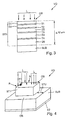
- FIG. 4 In the picture of the FIG. 4 is an embodiment of an advantageous juxtaposition of semiconductor layers to the first stack ST1 shown with a circumferential step-like step. The following are just the differences from the illustration of FIG. 3 explained.
- a first metallic connection contact K1 is formed on the edge R.
- the first connection contact K1 is connected to the first voltage connection VSUP1 - not shown.
- the substrate SUB has an upper side OS, wherein the upper side OS of the substrate SUB is materially connected to the lowermost, ie the fifth diode D5.
- a thin nucleation layer and a buffer layer are epitaxially generated on the substrate before the fifth diode is arranged on the substrate and connected in a materially bonded manner to the upper side OS of the substrate.
- the top side OS of the substrate SUB has a larger surface area than the bottom surface of the first stack ST1.
- a circulating stage STU is formed.
- the edge of the stage STU is removed from the immediately adjacent side surface of the first stack ST1 of the stage by more than 5 ⁇ m and less than 500 ⁇ m, shown as the length of the reference mark STU.
- a second full-surface metallic contact K2 educated.
- the second connection contact K2 is connected to the second voltage connection VSUP2 - not shown.
Landscapes
- Electrodes Of Semiconductors (AREA)
- Photovoltaic Devices (AREA)
- Light Receiving Elements (AREA)
- Control Of Electrical Variables (AREA)
- Photometry And Measurement Of Optical Pulse Characteristics (AREA)
- Life Sciences & Earth Sciences (AREA)
- Engineering & Computer Science (AREA)
- Sustainable Energy (AREA)
- Sustainable Development (AREA)
Abstract
Description
- Die Erfindung betrifft eine skalierbare Spannungsquelle.
- Aus der
US 4 127 862 , derUS 6 239 354 B1 , derDE 10 2010 001 420 A1 , aus Nader M. Kalkhoran, et al, "Cobalt disilicide intercell ohmic contacts for multijunction photovoltaic energy converters", Appl. Phys. Lett. 64, 1980 (1994) und aus A. Bett et al, "III-V Solar cells under monochromatic illumination", Photovoltaic Specialists Conference, 2008, PVSC '08. 33rd IEEE, Seite 1-5, ISBN:978-1-4244-1640-0 sind skalierbare Spannungsquellen oder auch Solarzellen aus III-V Materialien bekannt. - Vor diesem Hintergrund besteht die Aufgabe der Erfindung darin, eine Vorrichtung anzugeben, die den Stand der Technik weiterbildet.
- Die Aufgabe wird durch eine skalierbare Spannungsquelle mit den Merkmalen des Patentanspruchs 1 gelöst. Vorteilhafte Ausgestaltungen der Erfindung sind Gegenstand von Unteransprüchen.
- Gemäß dem Gegenstand der Erfindung wird skalierbare Spannungsquelle aufweisend eine Anzahl N zueinander in Serie geschalteten als Halbleiterdioden ausgebildete Teilspannungsquellen bereitgestellt, wobei jede der Teilspannungsquellen eine Halbleiterdiode mit einen p-n Übergang aufweist, und die Halbleiterdiode eine p-dotierte Absorptionsschicht aufweist, wobei die p-Absorptionsschicht von einer p-dotierten Passivierungsschicht mit einer größeren Bandlücke als die Bandlücke der p-Absorptionsschicht passiviert ist und die Halbleiterdiode eine n-Absorptionsschicht aufweist, wobei die n-Absorptionsschicht von einer n-dotierten Passivierungsschicht mit einer größeren Bandlücke als die Bandlücke der n-Absorptionsschicht passiviert ist, und die Teilquellenspannungen der einzelnen Teilspannungsquellen zueinander einer Abweichung kleiner als 20% aufweisen, und zwischen jeweils zwei aufeinanderfolgenden Teilspannungsquellen eine Tunneldiode ausgebildet ist, wobei die Tunneldiode mehrere Halbleiterschichten mit einer höheren Bandlücke als die Bandlücke der p / n Absorptionsschichten aufweist und die Halbleiterschichten mit der höheren Bandlücke jeweils aus einem Material mit geänderter Stöchiometrie und / oder anderer Elementzusammensetzung als die p / n -Absorptionsschichten der Halbleiterdiode bestehen, und die Teilspannungsquellen und die Tunneldioden zusammen monolithisch integriert sind, und gemeinsam einen ersten Stapel mit einer Oberseite und einer Unterseite ausbilden, und die Anzahl N der Teilspannungsquellen größer gleich drei ist, und das Licht an der Oberseite auf den ersten Stapel auftrifft und die Größe der Beleuchtungsfläche an der Stapeloberseite im Wesentlichen der Größe der Fläche des ersten Stapels an der Oberseite ist, und der erste Stapel eine Gesamtdicke kleiner als 12µm aufweist, und bei 300 K der erste Stapel eine Quellenspannung von größer als 3 Volt aufweist, sofern der erste Stapel mit einem Photonenstrom bestrahlt ist, und wobei in Lichteinfallsrichtung von der Oberseite des ersten Stapels hin zu der Unterseite des ersten Stapels die Gesamtdicke der p und n -Absorptionsschichten einer Halbleiterdiode von der obersten Diode hin zu der untersten Diode zunimmt und die Spannungsquelle in der Nähe der Unterseite der Stapel einen umlaufenden, absatzförmigen Rand aufweist.
- Es sei angemerkt, dass mit dem Ausdruck wesentlich in Zusammenhang des Vergleichs der Beleuchtungsfläche an der Stapeloberseite mit der Größe der Fläche des ersten Stapels an der Oberseite verstanden wird, einen Unterschied in der Fläche insbesondere kleiner als 20% oder vorzugsweise kleiner als 10% oder vorzugsweise kleiner als 5% oder höchst vorzugsweise die beiden Flächen gleich sind.
- Auch sei angemerkt, dass mit dem Ausdruck "Licht" zur Bestrahlung der Stapeloberseite, ein Licht verstanden wird, welches ein Spektrum an Wellenlängen in dem Bereich der Absorption der Absorptionsschichten aufweist. Es versteht sich, dass auch ein monochromatisches Licht, welches eine bestimmte d.h. absorbierende Wellenlänge aufweist, also eine Wellenlänge in dem Bereich der Absorption der Absorptionsschichten, geeignet ist.
- Es versteht sich, dass die vorzugsweise die gesamte Oberseite des ersten Stapels d.h. die gesamte oder nahezu die gesamte Oberfläche mit Licht einer bestimmten Wellenlänge bestrahlt wird. Es sei angemerkt, dass eingehende Untersuchungen in überraschender Weise zeigten, dass im Unterschied zu dem Stand der Technik sich in vorteilhafter Weise mit dem vorliegenden monolithischen Stapelansatz Quellenspannungen oberhalb von 3V ergeben.
- Ein Vorteil der erfindungsgemäßen Vorrichtung ist es, dass durch die Hintereinanderschaltung von einer Vielzahl von Teilspannungsquellen eine Spannungsquelle mit Spannungswerten auch oberhalb von vier oder mehr Volt sich mittels eines monolithisch integrierten Aufbau eine einfache und kostengünstige sowie eine zuverlässige Spannungsquelle herstellen lässt. Ein weiterer Vorteil ist, dass mittels der stapelförmigen Anordnung im Vergleich zu der bisherigen lateralen Anordnung mit Siliziumdioden eine große Flächeneinsparung ergibt. Insbesondere muss von der Sendediode oder der Lichtquelle nur die wesentlich kleinere Empfangsfläche des Stapels beleuchtet werden.
- In einer Weiterbildung weicht die Teilquellenspannungen der einzelnen Teilspannungsquellen untereinander weniger als 10% ab. Hierdurch wird die Einsetzbarkeit als skalierbare Spannungsquelle insbesondere als Referenzspannungsquelle wesentlich verbessert. Es versteht sich, dass sich der Begriff der "Skalierbarkeit" auf die Höhe der Quellenspannung des gesamten Stapels bezieht.
- In einer anderen Weiterbildung weisen die Halbleiterdioden jeweils das gleiche Halbleitermaterial auf, wobei hierbei das Halbleitermaterial der Dioden die gleiche kristalline Zusammensetzung aufweist und vorzugsweise die Stöchiometrie nahezu oder vorzugsweise genau gleich ist. Auch ist es vorteilhaft, den ersten Stapel auf einem Substrat anzuordnen. In einer Ausführungsform besteht das Halbleitermaterial und / oder das Substrat aus III-V Materialien. Insbesondere ist bevorzugt, dass das Substrat Germanium oder Galliumarsenid umfasst und / oder die Halbleiterschichten auf dem Substrat Arsen und / oder Phosphor aufweisen. Anders ausgedrückt umfassen die Halbleiterschichten As-haltige Schichten und P -haltige Schichten, d.h. Schichten aus GaAs oder AlGaAs oder InGaAs als Beispiele für Arsenid-Schichten und InGaP als ein Beispiel für Phosphid-Schichten.
- Es ist bevorzugt, auf der Unterseite des ersten Stapels ein zweiter Spannungsanschluss auszubilden und insbesondere, dass der zweite Spannungsanschluss durch das Substrat ausgebildet ist.
- In einer anderen Ausführungsform bestehen die Halbleiterdioden aus dem gleichen Material wie das Substrat. Ein Vorteil ist, dass sich dann insbesondere die Ausdehnungskoeffizienten der beiden Teile gleichen. Es ist vorteilhaft, wenn die Halbleiterdioden grundsätzlich aus einem III-V Material bestehen. Insbesondere ist es bevorzugt, GaAs zu verwenden.
- In einer bevorzugten Ausführungsform ist auf der Oberseite des ersten Stapels ein erster Spannungsanschluss als ein umlaufender Metallkontakt in der Nähe des Randes oder als einzelne Kontaktfläche an dem Rand ausgebildet.
- Des Weiteren ist es bevorzugt, wenn der erste Stapel eine Grundfläche kleiner als 2 mm2 oder kleiner als 1 mm2 aufweist. Untersuchungen haben gezeigt, dass es vorteilhaft ist, die Grundfläche viereckig auszubilden. Vorzugsweise ist die Grundfläche des Stapels quadratisch ausgebildet.
- Weitere Untersuchungen haben gezeigt, dass um besonderes hohe Spannungen zu erzielen es vorteilhaft ist, einen zweiten Stapel auszubilden und die beiden Stapel miteinander in Serie zu verschalten, so dass sich die Quellenspannung des ersten Stapels und die Quellenspannung des zweiten Stapels addieren. Vorzugsweise sind der erste Stapel und der zweite Stapel nebeneinander auf einem gemeinsamen Träger angeordnet.
- In einer Weiterbildung weicht die Quellenspannung des ersten Stapels von der Quellenspannung des zweiten Stapels um weniger als 15 % ab.
- Des Weiteren ist es bevorzugt, dass unterhalb der untersten Halbleiterdiode des Stapels ein Halbleiterspiegel ausgebildet ist. Untersuchungen haben gezeigt, dass sich eine Vielzahl von Stapeln nebeneinander auf einem Halbleiterwafer oder Halbleitersubstratscheibe ausbilden lassen, indem nach der ganzflächigen, vorzugsweise epitaktischen Herstellung der Schichten, eine sogenannte Mesaätzung durchgeführt wird. Hierzu wird mittels eines Maskenprozesses eine Lackmaske erzeugt und anschließend vorzugsweise eine naßchemische Ätzung zur Erzeugung von Mesa-Gräben durchgeführt. Die Mesaätzung stoppt vorzugsweise in dem Substrat oder auf dem Substrat.
- In einer Ausführungsform ist zwischen der p Absorptionsschicht und der n-Absorptionsschicht der jeweiligen Diode eine intrinsische Schicht ausgebildet. Hierbei wird unter einer intrinsischen Schicht eine Halbleiterschicht mit einer Dotierung unterhalb 1E16 1/cm2, vorzugsweise kleiner als 5E15 1/cm2, höchst vorzugsweise kleiner als 1,5 E15 1/ cm2 verstanden.
- In einer Weiterbildung ist es bevorzugt, dass jeder Stapel in der Nähe der Unterseite einen umlaufenden, absatzförmigen Rand aufweist, wobei bei zwei unmittelbar benachbarten Stapeln an den Außenseiten des Stapelgebildes der umlaufende Rand als ein gemeinsamer umlaufender Rand ausgebildet ist, so dass die Spannungsquelle einen umlaufenden Rand aufweist.
- Vorzugsweise ist der Rand stufenförmig oder als Stufe ausgebildet. Hierbei weist die Oberfläche des Randes bzw. der Stufe vorzugsweise größtenteils eine plane Fläche auf, wobei die Normale der Oberfläche des Randes bzw. der Stufe parallel oder nahezu parallel zu der Normalen der Oberfläche des ersten Stapels oder der Normalen der Oberflächen der jeweiligen Stapel ausgebildet ist. Es sei angemerkt dass die Seitenfläche des Randes oder der Stufe überwiegend oder genau senkrecht zu der Oberfläche des Randes bzw. der Stufe ausgebildet ist.
- Die Kante des Randes oder der Stufe ist wenigstens 5 µm und maximal 500 µm jeweils von jeder der vier Seitenflächen des ersten Stapels oder jeweils von den Seitenflächen der mehreren Stapeln entfernt. Vorzugsweise liegt der Entfernungsbereich jeweils der Kante zu der unmittelbar angrenzenden Seitenfläche zwischen 10 µm und 300 µm. Insbesondere liegt der Entfernungsbereich zwischen 50 µm und 250 µm.
- Vorzugsweise sind die Seitenflächen des ersten Stapels und insbesondere alle Seitenflächen der Stapel plan und insbesondere senkrecht oder nahezu senkrecht ausgebildet. Insbesondere liegen die Normalen auf Seitenflächen im Vergleich zu den Normalen der angrenzenden Randflächen oder den Normalen der Stapeloberflächen in einen Winkelbereich zwischen 80° und 110°, d.h. die Normalen einer Seitenfläche und der unmittelbar angrenzenden Randfläche sind zueinander im Wesentlichen Orthogonal. Vorzugsweise liegt der Winkelbereich zwischen 85° und 105°.
- Die Erfindung wird nachfolgend unter Bezugnahme auf die Zeichnungen näher erläutert. Hierbei werden gleichartige Teile mit identischen Bezeichnungen beschriftet. Die dargestellten Ausführungsformen sind stark schematisiert, d.h. die Abstände und die lateralen und die vertikalen Erstreckungen sind nicht maßstäblich und weisen, sofern nicht anders angegeben, auch keine ableitbaren geometrischen Relationen zueinander auf. Darin zeigt:
- Figur 1
- eine erste erfindungsgemäße Ausführungsform einer skalierbaren Spannungsquelle mit einem Stapel,
- Figur 2
- eine zweite Ausführungsform einer skallerbaren Spannungsquelle mit mehreren Stapeln,
- Figur 3
- eine Ausführungsform mit insgesamt fünf Dioden mit unterschiedlicher Dicke des Absorptionsgebiets,
- Figur 4
- eine Stapel mit einer umlaufenden absatzförmigen Stufe.
- Die Abbildung der
Figur 1 zeigt eine schematische Ansicht einer ersten Ausführungsform, aufweisend eine skalierbare Spannungsquelle VQ mit einem ersten Stapel ST1 mit einer Oberseite und einer Unterseite mit einer Anzahl N gleich drei Dioden. Der erste Stapel ST1 weist eine Serienschaltung aus einer ersten Diode D1 und einer ersten Tunneldiode T1 und einer zweiten Diode D2 und einer zweiten Tunneldiode T2 und einer dritten Diode D3 auf. An der Oberseite des Stapel ST1 ist ein erster Spannungsanschluss VSUP1 und der Unterseite des Stapel ST1 ein zweiter Spannungsanschluss VSUP2 ausgebildet. Die Quellenspannung VQ1 des ersten Stapel ST1 setzt sich vorliegend aus den Teilspannungen der einzelnen Dioden D1 bis D3 zusammen. Hierzu ist der erste Stapel ST1 einem Photonenstrom, d.h. dem Licht L ausgesetzt. - Der erste Stapel ST1 der Dioden D1 bis D3 und der Tunneldioden T1 und T2 ist als monolithisch ausgebildeter Block, vorzugsweise aus dem gleichen Halbleitermaterial, ausgeführt.
- In der Abbildung der
Figur 2 ist eine weitere Ausführungsform einer vorteilhaften Aneinanderreihung von dem ersten Stapel ST1 und einem zweiten Stapel ST2 ausgebildet. Im Folgenden werden nur die Unterschiede zu der Abbildung derFigur 1 erläutert. Der zweite Stapel ST2 weist wie der erste Stapel ST1 eine Serienschaltung aus drei Dioden mit dazwischen ausgebildeten Tunneldioden auf. Beide Stapel ST1 und ST2 sind miteinander in Serie verschaltet, sodass sich die Quellenspannung VQ1 des ersten Stapels ST1 und die Quellenspannung VQ2 des zweiten Stapel ST2 addieren, sofern die beiden Stapel ST1 und ST2 dem Photonenstrom L ausgesetzt sind. - In einer nicht dargestellten Ausführungsform weisen die beiden Stapel ST1 und ST2 zueinander eine unterschiedliche Anzahl von jeweils in einer Serienschaltung verbundenen Dioden auf. In einer anderen nicht dargestellten Ausführungsform weist wenigstens der erste Stapel ST1 und / oder der zweite Stapel ST2 mehr als drei in einer Serienschaltung verbundene Dioden auf. Hierdurch lässt sich die Spannungshöhe der Spannungsquelle VQ skalieren. Vorzugsweise liegt die Anzahl N in einem Bereich zwischen vier und acht. In einer Weiteren nicht dargestellten Ausführungsform, sind die beiden Stapel ST1 und ST2 zueinander parallel geschaltet.
- In der Abbildung der
Figur 3 ist eine Ausführungsform einer vorteilhaften Aneinanderreihung von Halbleiterschichten zu dem ersten Stapel ST1 dargestellt. Im Folgenden werden nur die Unterschiede zu der Abbildung derFigur 1 erläutert. Der erste Stapel ST1 umfasst insgesamt fünf in Reihe geschaltete als Dioden D1 bis D5 ausgebildete Teilspannungsquellen. Auf die Oberfläche OB der ersten Diode D1 trifft das Licht L auf. Die Oberfläche OB wird nahezu oder vollständig ausgeleuchtet. Zwischen zwei aufeinanderfolgenden Dioden D1-D5 ist jeweils eine Tunneldiode T1-T4 ausgebildet. Mit zunehmender Entfernung der einzelnen Diode D1 bis D5 von der Oberfläche OB steigt die Dicke des Absorptionsgebiets, so dass die unterste Diode D5 das dickste Absorptionsgebiet aufweist. Insgesamt beträgt die Gesamtdicke des ersten Stapels ST1 kleiner gleich 12 µm. Unterhalb der untersten Diode D5 ist ein Substrat SUB ausgebildet. - In der Abbildung der
Figur 4 ist eine Ausführungsform einer vorteilhaften Aneinanderreihung von Halbleiterschichten zu dem ersten Stapel ST1 dargestellt mit einer umlaufenden absatzförmigen Stufe. Im Folgenden werden nur die Unterschiede zu der Abbildung derFigur 3 erläutert. Auf der Oberfläche OB des ersten Stapels ST1 ist an dem Rand R ein erster metallischer Anschlusskontakt K1 ausgebildet. Der erste Anschlusskontakt K1 ist mit dem ersten Spannungsanschluss VSUP1 verschaltet - nicht dargestellt. Das Substrat SUB weist eine Oberseite OS auf, wobei die Oberseite OS des Substrats SUB stoffschlüssig mit der untersten, d.h. der fünften Diode D5 verbunden ist. Hierbei versteht es sich, dass auf dem Substrat eine dünne Nukleationsschicht und eine Pufferschicht epitaktisch erzeugt wird, bevor auf dem Substrat die fünfte Diode angeordnet wird und stoffschlüssig mit der Oberseite OS des Substrats verbunden wird. Die Oberseite OS des Substrats SUB weist eine größere Oberfläche als die Fläche an der Unterseite des ersten Stapels ST1 auf. Hierdurch bildet sich eine umlaufende Stufe STU aus. Der Rand der Stufe STU ist von der unmittelbar angrenzenden Seitenfläche des ersten Stapels ST1 der Stufe um mehr als 5µm und weniger als 500µm entfernt, dargestellt als Länge des Referenzzeichens STU. An der Unterseite des Substrats SUB ist ein zweiter ganzflächiger metallischer Kontakt K2 ausgebildet. Der zweite Anschlusskontakt K2 ist mit dem zweiten Spannungsanschluss VSUP2 verschaltet - nicht dargestellt.
Claims (16)
- Skalierbare Spannungsquelle (VQ) aufweisend- eine Anzahl N zueinander in Serie geschalteten als Halbleiterdioden ausgebildete Teilspannungsquellen, wobei jede der Teilspannungsquellen eine Halbleiterdiode (D1, D2, D3, D4, D5) mit einen p-n Übergang aufweist, und die Halbleiterdiode (D1, D2, D3, D4, D5) eine p-dotierte Absorptionsschicht aufweist und die Halbleiterdiode (D1, D2, D3, D4, D5) eine n-Absorptionsschicht aufweist, wobei die n-Absorptionsschicht von einer n-dotierten Passivierungsschicht mit einer größeren Bandlücke als die Bandlücke der n-Absorptionsschicht passiviert ist,
und die Teilquellenspannungen der einzelnen Teilspannungsquellen zueinander eine Abweichung kleiner als 20% aufweisen, und- zwischen jeweils zwei aufeinanderfolgenden Teilspannungsquellen eine Tunneldiode (T1, T2; T3, T4) ausgebildet ist, wobei
die Tunneldiode (T1, T2, T3, T4) mehrere Halbleiterschichten mit einer höheren Bandlücke als die Bandlücke der p / n Absorptionsschichten aufweist und die Halbleiterschichten mit der höheren Bandlücke jeweils aus einem Material mit geänderter Stöchiometrie und / oder anderer Elementzusammensetzung als die p / n -Absorptionsschichten der Halbleiterdiode (D1, D2, D3, D4, D5) bestehen, und- die Teilspannungsquellen und die Tunneldioden (T1, T2, T3, T4) zusammen monolithisch integriert sind, und gemeinsam einen ersten Stapel (ST1) mit einer Oberseite und einer Unterseite ausbilden, und die Anzahl N der Teilspannungsquellen größer gleich drei ist, und- bei einer Beleuchtung des ersten Stapels (ST1) mit Licht (L) wobei das Licht (L) an der Oberseite auf die Oberfläche (OB) auf den ersten Stapel (ST1) auftrifft und die Größe der beleuchteten Oberfläche (OB) an der Stapeloberseite im Wesentlichen der Größe der Fläche des ersten Stapels an der Oberseite entspricht, und
der erste Stapel (ST1) eine Gesamtdicke kleiner als 12µm aufweist, und- bei 300 K der erste Stapel (ST1) eine Quellenspannung (VQ1) von größer als 3 Volt aufweist, sofern der erste Stapel (ST1) mit Licht (L) bestrahlt ist, und wobei in Lichteinfallsrichtung von der Oberseite des ersten Stapels (ST1) hin zu der Unterseite des Stapels die Gesamtdicke der p und n -Absorptionsschichten einer Halbleiterdiode von der obersten Diode (D1) hin zu der untersten Diode (D3 - D5) zunimmt,dadurch gekennzeichnet, dass
jede p-Absorptionsschicht der Halbleiterdiode (D1, D2, D3, D4) von einer p-dotierten Passivierungsschicht mit einer größeren Bandlücke als die Bandlücke der p-Absorptionsschicht passiviert ist und die Spannungsquelle in der Nähe der Unterseite des ersten Stapels (ST1) einen umlaufenden, absatzförmigen Rand aufweist. - Skalierbare Spannungsquelle (VQ) nach Anspruch 1, dadurch gekennzeichnet, dass die Teilquellenspannungen der Teilspannungsquellen zueinander eine Abweichung kleiner als 10% aufweisen.
- Skalierbare Spannungsquelle (VQ) nach Anspruch 1 oder Anspruch 2, dadurch gekennzeichnet, dass die Halbleiterdioden (D1, D2, D3, D4, D5) jeweils das gleiche Halbleitermaterial aufweisen.
- Skalierbare Spannungsquelle (VQ) nach einem der vorangegangenen Ansprüche, dadurch gekennzeichnet, dass der erste Stapel (ST1) auf einem Substrat (SUB) angeordnet ist und das Substrat (SUB) ein Halbleitermaterial umfasst.
- Skalierbare Spannungsquelle (VQ) nach einem der vorangegangenen Ansprüche, dadurch gekennzeichnet, dass der erste Stapel (ST1) eine Grundfläche kleiner als 2 mm2 oder kleiner als 1 mm2 aufweist.
- Skalierbare Spannungsquelle (VQ) nach Anspruch 5, dadurch gekennzeichnet, dass die Grundfläche viereckig ausgebildet ist.
- Skalierbare Spannungsquelle (VQ) nach einem der vorangegangenen Ansprüche, dadurch gekennzeichnet, dass auf der Oberseite des ersten Stapels (ST1) ein erster Spannungsanschluss (VSUP1) als ein umlaufender erster Metallkontakt (K1) in der Nähe des Randes (R) oder als eine einzelne Kontaktfläche (K1) an dem Rand (R) ausgebildet ist.
- Skalierbare Spannungsquelle (VQ) nach einem der vorangegangenen Ansprüche, dadurch gekennzeichnet, dass auf der Unterseite des ersten Stapels (ST1) ein zweiter Spannungsanschluss (VSUP2) ausgebildet ist.
- Skalierbare Spannungsquelle (VQ) nach Anspruch 4 und / oder Anspruch 8 und / oder Anspruch 8, dadurch gekennzeichnet, dass der zweite Spannungsanschluss (VSUP2) durch das Substrat ausgebildet ist.
- Skalierbare Spannungsquelle (VQ) nach einem der vorangegangenen Ansprüche, dadurch gekennzeichnet, dass ein zweiter Stapel (ST2) ausgebildet ist und der erste Stapel (ST1) und der zweite Stapel (ST2) nebeneinander auf einem gemeinsamen Träger angeordnet sind und die beiden Stapel (ST1, ST2) miteinander in Serie verschaltet sind, so dass sich die Quellenspannung (VQ1) des ersten Stapels (ST1) und die Quellenspannung (VQ2) des zweiten Stapels (ST2) addieren.
- Skalierbare Spannungsquelle (VQ) nach einem der vorangegangenen Ansprüche, dadurch gekennzeichnet, dass zwischen der p Absorptionsschicht und der n-Absorptionsschicht der jeweiligen Diode eine intrinsische Schicht ausgebildet ist.
- Skalierbare Spannungsquelle (VQ) nach einem der vorangegangenen Ansprüche, dadurch gekennzeichnet, dass das Halbleitermaterial und / oder das Substrat aus III-V Materialien bestehen.
- Skalierbare Spannungsquelle (VQ) nach einem der vorangegangenen Ansprüche, dadurch gekennzeichnet, dass das Substrat Germanium oder Galliumarsenid umfasst.
- Skalierbare Spannungsquelle (VQ) nach einem der vorangegangenen Ansprüche, dadurch gekennzeichnet, dass unterhalb der untersten Halbleiterdiode des Stapels ein Halbleiterspiegel ausgebildet ist.
- Skalierbare Spannungsquelle (VQ) nach einem der vorangegangenen Ansprüche, dadurch gekennzeichnet, dass die Halbleiterschichten des Stapels (ST1) gleichzeitig Arsenid-haltige Schichten und Phosphidhaltige Schichten umfassen.
- Skalierbare Spannungsquelle (VQ) nach einem der vorangegangenen Ansprüche, dadurch gekennzeichnet, dass die Kante des Randes wenigstens 5 µm und maximal 500 µm von der unmittelbar angrenzenden Seitenfläche der Stapel entfernt ist.
Applications Claiming Priority (1)
| Application Number | Priority Date | Filing Date | Title |
|---|---|---|---|
| DE102015006379.0A DE102015006379B4 (de) | 2015-05-18 | 2015-05-18 | Skalierbare Spannungsquelle |
Publications (2)
| Publication Number | Publication Date |
|---|---|
| EP3096361A1 true EP3096361A1 (de) | 2016-11-23 |
| EP3096361B1 EP3096361B1 (de) | 2022-03-09 |
Family
ID=55963120
Family Applications (1)
| Application Number | Title | Priority Date | Filing Date |
|---|---|---|---|
| EP16001051.8A Active EP3096361B1 (de) | 2015-05-18 | 2016-05-10 | Skalierbare spannungsquelle |
Country Status (6)
| Country | Link |
|---|---|
| US (1) | US10872887B2 (de) |
| EP (1) | EP3096361B1 (de) |
| JP (1) | JP6312161B2 (de) |
| CN (2) | CN113745210A (de) |
| DE (1) | DE102015006379B4 (de) |
| TW (1) | TWI649891B (de) |
Cited By (1)
| Publication number | Priority date | Publication date | Assignee | Title |
|---|---|---|---|---|
| EP3144982A1 (de) * | 2015-09-19 | 2017-03-22 | AZUR SPACE Solar Power GmbH | Skalierbare spannungsquelle |
Families Citing this family (4)
| Publication number | Priority date | Publication date | Assignee | Title |
|---|---|---|---|---|
| DE102016001387A1 (de) * | 2016-02-09 | 2017-08-10 | Azur Space Solar Power Gmbh | Empfängerbaustein |
| US9865504B2 (en) | 2016-03-04 | 2018-01-09 | Taiwan Semiconductor Manufacturing Company, Ltd. | Semiconductor device and manufacturing method thereof |
| DE102017011643B4 (de) * | 2017-12-15 | 2020-05-14 | Azur Space Solar Power Gmbh | Optische Spannungsquelle |
| DE102019003069B4 (de) * | 2019-04-30 | 2023-06-01 | Azur Space Solar Power Gmbh | Stapelförmige hochsperrende lll-V-Halbleiterleistungsdioden |
Citations (5)
| Publication number | Priority date | Publication date | Assignee | Title |
|---|---|---|---|---|
| US4127862A (en) | 1977-09-06 | 1978-11-28 | Bell Telephone Laboratories, Incorporated | Integrated optical detectors |
| US6239354B1 (en) | 1998-10-09 | 2001-05-29 | Midwest Research Institute | Electrical isolation of component cells in monolithically interconnected modules |
| US20060048811A1 (en) * | 2004-09-09 | 2006-03-09 | Krut Dimitri D | Multijunction laser power converter |
| DE102010001420A1 (de) | 2010-02-01 | 2011-08-04 | Robert Bosch GmbH, 70469 | III-V-Halbleiter-Solarzelle |
| WO2014096200A1 (de) * | 2012-12-21 | 2014-06-26 | Fraunhofer-Gesellschaft zur Förderung der angewandten Forschung e. V. | Justagetolerante photovoltaische zelle |
Family Cites Families (75)
| Publication number | Priority date | Publication date | Assignee | Title |
|---|---|---|---|---|
| US4206002A (en) * | 1976-10-19 | 1980-06-03 | University Of Pittsburgh | Graded band gap multi-junction solar energy cell |
| US4179702A (en) * | 1978-03-09 | 1979-12-18 | Research Triangle Institute | Cascade solar cells |
| JPS55125680A (en) * | 1979-03-20 | 1980-09-27 | Yoshihiro Hamakawa | Photovoltaic element |
| US4688068A (en) * | 1983-07-08 | 1987-08-18 | The United States Of America As Represented By The Department Of Energy | Quantum well multijunction photovoltaic cell |
| US4598164A (en) * | 1983-10-06 | 1986-07-01 | Exxon Research And Engineering Co. | Solar cell made from amorphous superlattice material |
| US4667059A (en) * | 1985-10-22 | 1987-05-19 | The United States Of America As Represented By The United States Department Of Energy | Current and lattice matched tandem solar cell |
| US4631352A (en) * | 1985-12-17 | 1986-12-23 | The United States Of America As Represented By The Administrator Of The National Aeronautics And Space Administration | High band gap II-VI and III-V tunneling junctions for silicon multijunction solar cells |
| JPS62234379A (ja) * | 1986-04-04 | 1987-10-14 | Kanegafuchi Chem Ind Co Ltd | 半導体装置 |
| JP2719230B2 (ja) * | 1990-11-22 | 1998-02-25 | キヤノン株式会社 | 光起電力素子 |
| US5223043A (en) * | 1991-02-11 | 1993-06-29 | The United States Of America As Represented By The United States Department Of Energy | Current-matched high-efficiency, multijunction monolithic solar cells |
| US5298086A (en) * | 1992-05-15 | 1994-03-29 | United Solar Systems Corporation | Method for the manufacture of improved efficiency tandem photovoltaic device and device manufactured thereby |
| US5800630A (en) * | 1993-04-08 | 1998-09-01 | University Of Houston | Tandem solar cell with indium phosphide tunnel junction |
| US5407491A (en) * | 1993-04-08 | 1995-04-18 | University Of Houston | Tandem solar cell with improved tunnel junction |
| US6150603A (en) * | 1999-04-23 | 2000-11-21 | Hughes Electronics Corporation | Bilayer passivation structure for photovoltaic cells |
| JP3657143B2 (ja) * | 1999-04-27 | 2005-06-08 | シャープ株式会社 | 太陽電池及びその製造方法 |
| US6316715B1 (en) * | 2000-03-15 | 2001-11-13 | The Boeing Company | Multijunction photovoltaic cell with thin 1st (top) subcell and thick 2nd subcell of same or similar semiconductor material |
| US6864414B2 (en) * | 2001-10-24 | 2005-03-08 | Emcore Corporation | Apparatus and method for integral bypass diode in solar cells |
| JP2003218374A (ja) * | 2002-01-23 | 2003-07-31 | Sharp Corp | Iii−v族太陽電池 |
| US20060162768A1 (en) * | 2002-05-21 | 2006-07-27 | Wanlass Mark W | Low bandgap, monolithic, multi-bandgap, optoelectronic devices |
| US7122734B2 (en) * | 2002-10-23 | 2006-10-17 | The Boeing Company | Isoelectronic surfactant suppression of threading dislocations in metamorphic epitaxial layers |
| US6951819B2 (en) * | 2002-12-05 | 2005-10-04 | Blue Photonics, Inc. | High efficiency, monolithic multijunction solar cells containing lattice-mismatched materials and methods of forming same |
| US7488890B2 (en) * | 2003-04-21 | 2009-02-10 | Sharp Kabushiki Kaisha | Compound solar battery and manufacturing method thereof |
| DE102004023856B4 (de) | 2004-05-12 | 2006-07-13 | Rwe Space Solar Power Gmbh | Solarzelle mit integrierter Schutzdiode und zusätzlich auf dieser angeordneten Tunneldiode |
| DE102004044061A1 (de) | 2004-09-11 | 2006-04-20 | Rwe Space Solar Power Gmbh | Solarzellenanordung sowie Verfahren zum Verschalten eines Solarzellenstrings |
| DE102005000767A1 (de) * | 2005-01-04 | 2006-07-20 | Rwe Space Solar Power Gmbh | Monolithische Mehrfach-Solarzelle |
| JP4868746B2 (ja) * | 2005-02-16 | 2012-02-01 | シャープ株式会社 | 薄膜化合物太陽電池およびその製造方法 |
| KR20080013979A (ko) * | 2005-05-03 | 2008-02-13 | 유니버시티 오브 델라웨어 | 초고효율 태양 전지 |
| US20100147381A1 (en) * | 2005-07-13 | 2010-06-17 | Haney Michael W | Ultra and very high efficiency solar cells |
| US8795854B2 (en) * | 2005-08-01 | 2014-08-05 | Amit Goyal | Semiconductor-based, large-area, flexible, electronic devices on {110}<100> oriented substrates |
| US8742251B2 (en) | 2006-12-20 | 2014-06-03 | Jds Uniphase Corporation | Multi-segment photovoltaic power converter with a center portion |
| JP2008177212A (ja) * | 2007-01-16 | 2008-07-31 | Nec Corp | 半導体受光素子 |
| WO2008124154A2 (en) * | 2007-04-09 | 2008-10-16 | Amberwave Systems Corporation | Photovoltaics on silicon |
| US8895342B2 (en) * | 2007-09-24 | 2014-11-25 | Emcore Solar Power, Inc. | Heterojunction subcells in inverted metamorphic multijunction solar cells |
| US20090188554A1 (en) * | 2008-01-25 | 2009-07-30 | Emcore Corporation | III-V Compound Semiconductor Solar Cell for Terrestrial Solar Array |
| US20090215215A1 (en) * | 2008-02-21 | 2009-08-27 | Sunlight Photonics Inc. | Method and apparatus for manufacturing multi-layered electro-optic devices |
| JP5203397B2 (ja) * | 2008-02-21 | 2013-06-05 | シャープ株式会社 | 太陽電池の製造方法 |
| US8075723B1 (en) * | 2008-03-03 | 2011-12-13 | Stion Corporation | Laser separation method for manufacture of unit cells for thin film photovoltaic materials |
| US20090325340A1 (en) * | 2008-06-30 | 2009-12-31 | Mohd Aslami | Plasma vapor deposition system and method for making multi-junction silicon thin film solar cell modules and panels |
| US8298856B2 (en) * | 2008-07-17 | 2012-10-30 | Uriel Solar, Inc. | Polycrystalline CDTE thin film semiconductor photovoltaic cell structures for use in solar electricity generation |
| US9080425B2 (en) * | 2008-10-17 | 2015-07-14 | Foro Energy, Inc. | High power laser photo-conversion assemblies, apparatuses and methods of use |
| US8916769B2 (en) * | 2008-10-01 | 2014-12-23 | International Business Machines Corporation | Tandem nanofilm interconnected semiconductor wafer solar cells |
| US8138410B2 (en) * | 2008-10-01 | 2012-03-20 | International Business Machines Corporation | Optical tandem photovoltaic cell panels |
| US8912428B2 (en) * | 2008-10-22 | 2014-12-16 | Epir Technologies, Inc. | High efficiency multijunction II-VI photovoltaic solar cells |
| US20100122764A1 (en) * | 2008-11-14 | 2010-05-20 | Emcore Solar Power, Inc. | Surrogate Substrates for Inverted Metamorphic Multijunction Solar Cells |
| JP5570736B2 (ja) * | 2009-02-06 | 2014-08-13 | シャープ株式会社 | 化合物半導体太陽電池の製造方法 |
| US8299351B2 (en) * | 2009-02-24 | 2012-10-30 | Hong Kong Applied Science And Technology Research Institute Co., Ltd. | Epitaxial growth of III-V compounds on (111) silicon for solar cells |
| US9722131B2 (en) * | 2009-03-16 | 2017-08-01 | The Boeing Company | Highly doped layer for tunnel junctions in solar cells |
| US10505062B2 (en) * | 2009-07-09 | 2019-12-10 | Faquir Chand Jain | High efficiency tandem solar cells and a method for fabricating same |
| TWI409959B (zh) * | 2009-12-07 | 2013-09-21 | Epistar Corp | 太陽能電池元件及其裝置 |
| JP5215284B2 (ja) * | 2009-12-25 | 2013-06-19 | シャープ株式会社 | 多接合型化合物半導体太陽電池 |
| US8852994B2 (en) * | 2010-05-24 | 2014-10-07 | Masimo Semiconductor, Inc. | Method of fabricating bifacial tandem solar cells |
| US11417788B2 (en) * | 2010-11-19 | 2022-08-16 | The Boeing Company | Type-II high bandgap tunnel junctions of InP lattice constant for multijunction solar cells |
| DE102011000521A1 (de) * | 2011-02-04 | 2012-08-23 | Azur Space Solar Power Gmbh | Mehrfachsolarzelle sowie Verfahren zur Herstellung einer solchen |
| CN103477448B (zh) * | 2011-03-29 | 2016-11-09 | 加州理工学院 | 基于石墨烯的多结柔性太阳能电池 |
| WO2012147141A1 (ja) * | 2011-04-27 | 2012-11-01 | パナソニック株式会社 | 太陽電池を用いて電力を発生させる方法 |
| US20120285519A1 (en) * | 2011-05-10 | 2012-11-15 | Emcore Solar Power, Inc. | Grid design for iii-v compound semiconductor cell |
| US10340401B2 (en) * | 2011-09-22 | 2019-07-02 | The Boeing Company | Multi-layer back surface field layer in a solar cell structure |
| KR20140095062A (ko) * | 2011-10-21 | 2014-07-31 | 유니버시티 오브 유타 리서치 파운데이션 | 균질한 다중 밴드 갭 디바이스 |
| US8912617B2 (en) * | 2011-10-27 | 2014-12-16 | Solar Junction Corporation | Method for making semiconductor light detection devices |
| WO2013074530A2 (en) * | 2011-11-15 | 2013-05-23 | Solar Junction Corporation | High efficiency multijunction solar cells |
| US9263611B2 (en) * | 2011-11-17 | 2016-02-16 | Solar Junction Corporation | Method for etching multi-layer epitaxial material |
| EP2763186A4 (de) | 2011-12-14 | 2015-01-07 | Panasonic Corp | Solarzelle und verfahren zu ihrer herstellung |
| EP2618385A1 (de) * | 2012-01-20 | 2013-07-24 | AZUR SPACE Solar Power GmbH | Halbzeug einer Mehrfachsolarzelle und Verfahren zur Herstellung einer Mehrfachsolarzelle |
| CN102651416A (zh) * | 2012-05-18 | 2012-08-29 | 中国科学院苏州纳米技术与纳米仿生研究所 | 三结叠层GaAs激光光伏电池及其制备方法 |
| WO2013192559A1 (en) * | 2012-06-22 | 2013-12-27 | Izar Solar Inc | Manufacturing semiconductor-based multi-junction photovoltaic devices |
| US9099595B2 (en) * | 2012-09-14 | 2015-08-04 | The Boeing Company | Group-IV solar cell structure using group-IV or III-V heterostructures |
| US9997659B2 (en) * | 2012-09-14 | 2018-06-12 | The Boeing Company | Group-IV solar cell structure using group-IV or III-V heterostructures |
| US9985160B2 (en) * | 2012-09-14 | 2018-05-29 | The Boeing Company | Group-IV solar cell structure using group-IV or III-V heterostructures |
| US9530911B2 (en) * | 2013-03-14 | 2016-12-27 | The Boeing Company | Solar cell structures for improved current generation and collection |
| ITMI20131297A1 (it) * | 2013-08-01 | 2015-02-02 | Cesi Ct Elettrotecnico Sperim Entale Italian | Cella fotovoltaica con banda proibita variabile |
| US10340699B2 (en) * | 2013-09-11 | 2019-07-02 | Japan Aerospace Exploration Agency | Solar cell adjustment system, related method, and minimum current detection and control system |
| CN103594539B (zh) * | 2013-10-22 | 2016-02-10 | 扬州乾照光电有限公司 | 一种柔性多结GaAs太阳电池及其制备方法 |
| CN103545389B (zh) * | 2013-10-24 | 2016-03-30 | 瑞德兴阳新能源技术有限公司 | 一种多结聚光砷化镓太阳能电池及其制备方法 |
| US20170018675A1 (en) * | 2014-04-11 | 2017-01-19 | Semprius, Inc. | Multi-junction photovoltaic micro-cell architectures for energy harvesting and/or laser power conversion |
| US20150295114A1 (en) * | 2014-04-11 | 2015-10-15 | Sempruis, Inc. | Multi-junction power converter with photon recycling |
-
2015
- 2015-05-18 DE DE102015006379.0A patent/DE102015006379B4/de active Active
-
2016
- 2016-05-10 EP EP16001051.8A patent/EP3096361B1/de active Active
- 2016-05-12 TW TW105114779A patent/TWI649891B/zh active
- 2016-05-16 CN CN202111000142.4A patent/CN113745210A/zh active Pending
- 2016-05-16 CN CN201610322917.2A patent/CN106169468A/zh active Pending
- 2016-05-18 US US15/158,051 patent/US10872887B2/en active Active
- 2016-05-18 JP JP2016099317A patent/JP6312161B2/ja active Active
Patent Citations (5)
| Publication number | Priority date | Publication date | Assignee | Title |
|---|---|---|---|---|
| US4127862A (en) | 1977-09-06 | 1978-11-28 | Bell Telephone Laboratories, Incorporated | Integrated optical detectors |
| US6239354B1 (en) | 1998-10-09 | 2001-05-29 | Midwest Research Institute | Electrical isolation of component cells in monolithically interconnected modules |
| US20060048811A1 (en) * | 2004-09-09 | 2006-03-09 | Krut Dimitri D | Multijunction laser power converter |
| DE102010001420A1 (de) | 2010-02-01 | 2011-08-04 | Robert Bosch GmbH, 70469 | III-V-Halbleiter-Solarzelle |
| WO2014096200A1 (de) * | 2012-12-21 | 2014-06-26 | Fraunhofer-Gesellschaft zur Förderung der angewandten Forschung e. V. | Justagetolerante photovoltaische zelle |
Non-Patent Citations (4)
| Title |
|---|
| A. BETT ET AL.: "III-V Solar cells under monochromatic illumination", PHOTOVOLTAIC SPECIALISTS CONFERENCE, 2008, PVSC '08. 33RD IEEE, pages 1 - 5 |
| NADER M. KALKHORAN ET AL.: "Cobalt disilicide intercell ohmic contacts for multijunction photovoltaic energy converters", APPL. PHYS. LETT., vol. 64, 1994, pages 1980, XP000440949, DOI: doi:10.1063/1.111713 |
| SCHUBERT J ET AL: "High-Voltage GaAs Photovoltaic Laser Power Converters", IEEE TRANSACTIONS ON ELECTRON DEVICES, IEEE SERVICE CENTER, PISACATAWAY, NJ, US, vol. 56, no. 2, February 2009 (2009-02-01), pages 170 - 175, XP011241423, ISSN: 0018-9383, DOI: 10.1109/TED.2008.2010603 * |
| VALDIVIA CHRISTOPHER E ET AL: "Five-volt vertically-stacked, single-cell GaAs photonic power converter", PROCEEDINGS OF SPIE, vol. 9358, 16 March 2015 (2015-03-16), pages 93580E-1 - 93580E-8, XP060049977, ISBN: 978-1-62841-730-2, DOI: 10.1117/12.2079824 * |
Cited By (2)
| Publication number | Priority date | Publication date | Assignee | Title |
|---|---|---|---|---|
| EP3144982A1 (de) * | 2015-09-19 | 2017-03-22 | AZUR SPACE Solar Power GmbH | Skalierbare spannungsquelle |
| US9741874B2 (en) | 2015-09-19 | 2017-08-22 | Azur Space Solar Power Gmbh | Scalable voltage source |
Also Published As
| Publication number | Publication date |
|---|---|
| JP2016219012A (ja) | 2016-12-22 |
| TW201707226A (zh) | 2017-02-16 |
| CN113745210A (zh) | 2021-12-03 |
| DE102015006379A1 (de) | 2016-11-24 |
| EP3096361B1 (de) | 2022-03-09 |
| US20160343704A1 (en) | 2016-11-24 |
| US10872887B2 (en) | 2020-12-22 |
| DE102015006379B4 (de) | 2022-03-17 |
| TWI649891B (zh) | 2019-02-01 |
| JP6312161B2 (ja) | 2018-04-18 |
| CN106169468A (zh) | 2016-11-30 |
Similar Documents
| Publication | Publication Date | Title |
|---|---|---|
| EP3104422B1 (de) | Optokoppler | |
| DE102008034711B4 (de) | Invertierte metamorphe Multijunction-Solarzelle mit Barrierenschicht und Verfahren zur Herstellung | |
| EP3144982B1 (de) | Skalierbare spannungsquelle | |
| EP3096361B1 (de) | Skalierbare spannungsquelle | |
| DE60033252T2 (de) | Mehrschichtige halbleiter-struktur mit phosphid-passiviertem germanium-substrat | |
| EP3179521A1 (de) | Mehrfach-solarzelle | |
| EP3324451A1 (de) | Stapelförmige halbleiterstruktur | |
| EP3185312A1 (de) | Stapelförmige mehrfach-solarzelle | |
| DE69005048T2 (de) | Matrix von Heteroübergang-Photodioden. | |
| EP2803092A1 (de) | Solarzellenstapel | |
| EP3012874A1 (de) | Stapelförmige integrierte Mehrfachsolarzelle | |
| DE102013000882B3 (de) | Halbleiterbauelement mit Härtepuffer und dessen Verwendung | |
| EP3018718A1 (de) | Solarzellenstapel | |
| DE102015013514B4 (de) | Optischer Empfängerbaustein | |
| EP3667742A1 (de) | Stapelförmige monolithische aufrecht-metamorphe mehrfachsolarzelle | |
| DE102013211231B4 (de) | Verfahren zum Bilden einer Tandem-Fotovoltaikeinheit | |
| WO2017137151A1 (de) | Empfängerbaustein | |
| DE112012004680T5 (de) | Bypass-Diode | |
| EP3965168B1 (de) | Stapelförmige monolithische mehrfachsolarzelle | |
| DE102016005640A1 (de) | Invertierte Mehrfach-Solarzelle | |
| EP3965169B1 (de) | Stapelförmige monolithische mehrfachsolarzelle | |
| WO2017137150A1 (de) | Optokoppler | |
| DE102009057020B4 (de) | Wachstumssubstrate für invertierte metamorphe Multijunction-Solarzellen | |
| EP2991124A1 (de) | Stapelförmige integrierte Mehrfachsolarzelle und Verfahren zur Herstellung einer stapelförmigen integrierten Mehrfachsolarzelle | |
| EP3937258A1 (de) | Monolithische metamorphe mehrfachsolarzelle |
Legal Events
| Date | Code | Title | Description |
|---|---|---|---|
| PUAI | Public reference made under article 153(3) epc to a published international application that has entered the european phase |
Free format text: ORIGINAL CODE: 0009012 |
|
| AK | Designated contracting states |
Kind code of ref document: A1 Designated state(s): AL AT BE BG CH CY CZ DE DK EE ES FI FR GB GR HR HU IE IS IT LI LT LU LV MC MK MT NL NO PL PT RO RS SE SI SK SM TR |
|
| AX | Request for extension of the european patent |
Extension state: BA ME |
|
| STAA | Information on the status of an ep patent application or granted ep patent |
Free format text: STATUS: REQUEST FOR EXAMINATION WAS MADE |
|
| 17P | Request for examination filed |
Effective date: 20161124 |
|
| RBV | Designated contracting states (corrected) |
Designated state(s): AL AT BE BG CH CY CZ DE DK EE ES FI FR GB GR HR HU IE IS IT LI LT LU LV MC MK MT NL NO PL PT RO RS SE SI SK SM TR |
|
| STAA | Information on the status of an ep patent application or granted ep patent |
Free format text: STATUS: EXAMINATION IS IN PROGRESS |
|
| 17Q | First examination report despatched |
Effective date: 20200909 |
|
| GRAP | Despatch of communication of intention to grant a patent |
Free format text: ORIGINAL CODE: EPIDOSNIGR1 |
|
| STAA | Information on the status of an ep patent application or granted ep patent |
Free format text: STATUS: GRANT OF PATENT IS INTENDED |
|
| INTG | Intention to grant announced |
Effective date: 20211222 |
|
| GRAS | Grant fee paid |
Free format text: ORIGINAL CODE: EPIDOSNIGR3 |
|
| GRAA | (expected) grant |
Free format text: ORIGINAL CODE: 0009210 |
|
| STAA | Information on the status of an ep patent application or granted ep patent |
Free format text: STATUS: THE PATENT HAS BEEN GRANTED |
|
| AK | Designated contracting states |
Kind code of ref document: B1 Designated state(s): AL AT BE BG CH CY CZ DE DK EE ES FI FR GB GR HR HU IE IS IT LI LT LU LV MC MK MT NL NO PL PT RO RS SE SI SK SM TR |
|
| REG | Reference to a national code |
Ref country code: GB Ref legal event code: FG4D Free format text: NOT ENGLISH |
|
| REG | Reference to a national code |
Ref country code: CH Ref legal event code: EP Ref country code: AT Ref legal event code: REF Ref document number: 1474872 Country of ref document: AT Kind code of ref document: T Effective date: 20220315 |
|
| REG | Reference to a national code |
Ref country code: DE Ref legal event code: R096 Ref document number: 502016014593 Country of ref document: DE |
|
| REG | Reference to a national code |
Ref country code: IE Ref legal event code: FG4D Free format text: LANGUAGE OF EP DOCUMENT: GERMAN |
|
| REG | Reference to a national code |
Ref country code: FI Ref legal event code: FGE |
|
| REG | Reference to a national code |
Ref country code: LT Ref legal event code: MG9D |
|
| REG | Reference to a national code |
Ref country code: NL Ref legal event code: MP Effective date: 20220309 |
|
| PG25 | Lapsed in a contracting state [announced via postgrant information from national office to epo] |
Ref country code: SE Free format text: LAPSE BECAUSE OF FAILURE TO SUBMIT A TRANSLATION OF THE DESCRIPTION OR TO PAY THE FEE WITHIN THE PRESCRIBED TIME-LIMIT Effective date: 20220309 Ref country code: RS Free format text: LAPSE BECAUSE OF FAILURE TO SUBMIT A TRANSLATION OF THE DESCRIPTION OR TO PAY THE FEE WITHIN THE PRESCRIBED TIME-LIMIT Effective date: 20220309 Ref country code: NO Free format text: LAPSE BECAUSE OF FAILURE TO SUBMIT A TRANSLATION OF THE DESCRIPTION OR TO PAY THE FEE WITHIN THE PRESCRIBED TIME-LIMIT Effective date: 20220609 Ref country code: LT Free format text: LAPSE BECAUSE OF FAILURE TO SUBMIT A TRANSLATION OF THE DESCRIPTION OR TO PAY THE FEE WITHIN THE PRESCRIBED TIME-LIMIT Effective date: 20220309 Ref country code: HR Free format text: LAPSE BECAUSE OF FAILURE TO SUBMIT A TRANSLATION OF THE DESCRIPTION OR TO PAY THE FEE WITHIN THE PRESCRIBED TIME-LIMIT Effective date: 20220309 Ref country code: BG Free format text: LAPSE BECAUSE OF FAILURE TO SUBMIT A TRANSLATION OF THE DESCRIPTION OR TO PAY THE FEE WITHIN THE PRESCRIBED TIME-LIMIT Effective date: 20220609 |
|
| PG25 | Lapsed in a contracting state [announced via postgrant information from national office to epo] |
Ref country code: LV Free format text: LAPSE BECAUSE OF FAILURE TO SUBMIT A TRANSLATION OF THE DESCRIPTION OR TO PAY THE FEE WITHIN THE PRESCRIBED TIME-LIMIT Effective date: 20220309 Ref country code: GR Free format text: LAPSE BECAUSE OF FAILURE TO SUBMIT A TRANSLATION OF THE DESCRIPTION OR TO PAY THE FEE WITHIN THE PRESCRIBED TIME-LIMIT Effective date: 20220610 |
|
| PG25 | Lapsed in a contracting state [announced via postgrant information from national office to epo] |
Ref country code: NL Free format text: LAPSE BECAUSE OF FAILURE TO SUBMIT A TRANSLATION OF THE DESCRIPTION OR TO PAY THE FEE WITHIN THE PRESCRIBED TIME-LIMIT Effective date: 20220309 |
|
| PG25 | Lapsed in a contracting state [announced via postgrant information from national office to epo] |
Ref country code: SM Free format text: LAPSE BECAUSE OF FAILURE TO SUBMIT A TRANSLATION OF THE DESCRIPTION OR TO PAY THE FEE WITHIN THE PRESCRIBED TIME-LIMIT Effective date: 20220309 Ref country code: SK Free format text: LAPSE BECAUSE OF FAILURE TO SUBMIT A TRANSLATION OF THE DESCRIPTION OR TO PAY THE FEE WITHIN THE PRESCRIBED TIME-LIMIT Effective date: 20220309 Ref country code: RO Free format text: LAPSE BECAUSE OF FAILURE TO SUBMIT A TRANSLATION OF THE DESCRIPTION OR TO PAY THE FEE WITHIN THE PRESCRIBED TIME-LIMIT Effective date: 20220309 Ref country code: PT Free format text: LAPSE BECAUSE OF FAILURE TO SUBMIT A TRANSLATION OF THE DESCRIPTION OR TO PAY THE FEE WITHIN THE PRESCRIBED TIME-LIMIT Effective date: 20220711 Ref country code: ES Free format text: LAPSE BECAUSE OF FAILURE TO SUBMIT A TRANSLATION OF THE DESCRIPTION OR TO PAY THE FEE WITHIN THE PRESCRIBED TIME-LIMIT Effective date: 20220309 Ref country code: EE Free format text: LAPSE BECAUSE OF FAILURE TO SUBMIT A TRANSLATION OF THE DESCRIPTION OR TO PAY THE FEE WITHIN THE PRESCRIBED TIME-LIMIT Effective date: 20220309 Ref country code: CZ Free format text: LAPSE BECAUSE OF FAILURE TO SUBMIT A TRANSLATION OF THE DESCRIPTION OR TO PAY THE FEE WITHIN THE PRESCRIBED TIME-LIMIT Effective date: 20220309 |
|
| PG25 | Lapsed in a contracting state [announced via postgrant information from national office to epo] |
Ref country code: PL Free format text: LAPSE BECAUSE OF FAILURE TO SUBMIT A TRANSLATION OF THE DESCRIPTION OR TO PAY THE FEE WITHIN THE PRESCRIBED TIME-LIMIT Effective date: 20220309 Ref country code: IS Free format text: LAPSE BECAUSE OF FAILURE TO SUBMIT A TRANSLATION OF THE DESCRIPTION OR TO PAY THE FEE WITHIN THE PRESCRIBED TIME-LIMIT Effective date: 20220709 Ref country code: AL Free format text: LAPSE BECAUSE OF FAILURE TO SUBMIT A TRANSLATION OF THE DESCRIPTION OR TO PAY THE FEE WITHIN THE PRESCRIBED TIME-LIMIT Effective date: 20220309 |
|
| REG | Reference to a national code |
Ref country code: DE Ref legal event code: R097 Ref document number: 502016014593 Country of ref document: DE |
|
| REG | Reference to a national code |
Ref country code: CH Ref legal event code: PL |
|
| PLBE | No opposition filed within time limit |
Free format text: ORIGINAL CODE: 0009261 |
|
| STAA | Information on the status of an ep patent application or granted ep patent |
Free format text: STATUS: NO OPPOSITION FILED WITHIN TIME LIMIT |
|
| PG25 | Lapsed in a contracting state [announced via postgrant information from national office to epo] |
Ref country code: MC Free format text: LAPSE BECAUSE OF FAILURE TO SUBMIT A TRANSLATION OF THE DESCRIPTION OR TO PAY THE FEE WITHIN THE PRESCRIBED TIME-LIMIT Effective date: 20220309 Ref country code: LU Free format text: LAPSE BECAUSE OF NON-PAYMENT OF DUE FEES Effective date: 20220510 Ref country code: LI Free format text: LAPSE BECAUSE OF NON-PAYMENT OF DUE FEES Effective date: 20220531 Ref country code: DK Free format text: LAPSE BECAUSE OF FAILURE TO SUBMIT A TRANSLATION OF THE DESCRIPTION OR TO PAY THE FEE WITHIN THE PRESCRIBED TIME-LIMIT Effective date: 20220309 Ref country code: CH Free format text: LAPSE BECAUSE OF NON-PAYMENT OF DUE FEES Effective date: 20220531 |
|
| 26N | No opposition filed |
Effective date: 20221212 |
|
| PG25 | Lapsed in a contracting state [announced via postgrant information from national office to epo] |
Ref country code: SI Free format text: LAPSE BECAUSE OF FAILURE TO SUBMIT A TRANSLATION OF THE DESCRIPTION OR TO PAY THE FEE WITHIN THE PRESCRIBED TIME-LIMIT Effective date: 20220309 |
|
| REG | Reference to a national code |
Ref country code: AT Ref legal event code: MM01 Ref document number: 1474872 Country of ref document: AT Kind code of ref document: T Effective date: 20220510 |
|
| PG25 | Lapsed in a contracting state [announced via postgrant information from national office to epo] |
Ref country code: AT Free format text: LAPSE BECAUSE OF NON-PAYMENT OF DUE FEES Effective date: 20220510 |
|
| PG25 | Lapsed in a contracting state [announced via postgrant information from national office to epo] |
Ref country code: HU Free format text: LAPSE BECAUSE OF FAILURE TO SUBMIT A TRANSLATION OF THE DESCRIPTION OR TO PAY THE FEE WITHIN THE PRESCRIBED TIME-LIMIT; INVALID AB INITIO Effective date: 20160510 |
|
| PG25 | Lapsed in a contracting state [announced via postgrant information from national office to epo] |
Ref country code: MK Free format text: LAPSE BECAUSE OF FAILURE TO SUBMIT A TRANSLATION OF THE DESCRIPTION OR TO PAY THE FEE WITHIN THE PRESCRIBED TIME-LIMIT Effective date: 20220309 Ref country code: CY Free format text: LAPSE BECAUSE OF FAILURE TO SUBMIT A TRANSLATION OF THE DESCRIPTION OR TO PAY THE FEE WITHIN THE PRESCRIBED TIME-LIMIT Effective date: 20220309 |
|
| PG25 | Lapsed in a contracting state [announced via postgrant information from national office to epo] |
Ref country code: TR Free format text: LAPSE BECAUSE OF FAILURE TO SUBMIT A TRANSLATION OF THE DESCRIPTION OR TO PAY THE FEE WITHIN THE PRESCRIBED TIME-LIMIT Effective date: 20220309 |
|
| P01 | Opt-out of the competence of the unified patent court (upc) registered |
Free format text: CASE NUMBER: APP_40018/2024 Effective date: 20240704 |
|
| PG25 | Lapsed in a contracting state [announced via postgrant information from national office to epo] |
Ref country code: MT Free format text: LAPSE BECAUSE OF FAILURE TO SUBMIT A TRANSLATION OF THE DESCRIPTION OR TO PAY THE FEE WITHIN THE PRESCRIBED TIME-LIMIT Effective date: 20220309 |
|
| REG | Reference to a national code |
Ref country code: DE Ref legal event code: R079 Ref document number: 502016014593 Country of ref document: DE Free format text: PREVIOUS MAIN CLASS: H01L0031068700 Ipc: H10F0010142000 |
|
| PGFP | Annual fee paid to national office [announced via postgrant information from national office to epo] |
Ref country code: FI Payment date: 20250526 Year of fee payment: 10 |
|
| PGFP | Annual fee paid to national office [announced via postgrant information from national office to epo] |
Ref country code: DE Payment date: 20250521 Year of fee payment: 10 |
|
| PGFP | Annual fee paid to national office [announced via postgrant information from national office to epo] |
Ref country code: GB Payment date: 20250527 Year of fee payment: 10 |
|
| PGFP | Annual fee paid to national office [announced via postgrant information from national office to epo] |
Ref country code: BE Payment date: 20250521 Year of fee payment: 10 Ref country code: IT Payment date: 20250527 Year of fee payment: 10 |
|
| PGFP | Annual fee paid to national office [announced via postgrant information from national office to epo] |
Ref country code: FR Payment date: 20250528 Year of fee payment: 10 |
|
| PGFP | Annual fee paid to national office [announced via postgrant information from national office to epo] |
Ref country code: IE Payment date: 20250521 Year of fee payment: 10 |