EP3192645A1 - Herstellungsverfahren eines bildschirms, der mit rückstrahlenden mikrostrukturen ausgestattet ist - Google Patents
Herstellungsverfahren eines bildschirms, der mit rückstrahlenden mikrostrukturen ausgestattet ist Download PDFInfo
- Publication number
- EP3192645A1 EP3192645A1 EP17150779.1A EP17150779A EP3192645A1 EP 3192645 A1 EP3192645 A1 EP 3192645A1 EP 17150779 A EP17150779 A EP 17150779A EP 3192645 A1 EP3192645 A1 EP 3192645A1
- Authority
- EP
- European Patent Office
- Prior art keywords
- substrate
- layer
- screen
- face
- front face
- Prior art date
- Legal status (The legal status is an assumption and is not a legal conclusion. Google has not performed a legal analysis and makes no representation as to the accuracy of the status listed.)
- Granted
Links
Images


Classifications
-
- B—PERFORMING OPERATIONS; TRANSPORTING
- B29—WORKING OF PLASTICS; WORKING OF SUBSTANCES IN A PLASTIC STATE IN GENERAL
- B29C—SHAPING OR JOINING OF PLASTICS; SHAPING OF MATERIAL IN A PLASTIC STATE, NOT OTHERWISE PROVIDED FOR; AFTER-TREATMENT OF THE SHAPED PRODUCTS, e.g. REPAIRING
- B29C33/00—Moulds or cores; Details thereof or accessories therefor
- B29C33/42—Moulds or cores; Details thereof or accessories therefor characterised by the shape of the moulding surface, e.g. ribs or grooves
-
- B—PERFORMING OPERATIONS; TRANSPORTING
- B29—WORKING OF PLASTICS; WORKING OF SUBSTANCES IN A PLASTIC STATE IN GENERAL
- B29D—PRODUCING PARTICULAR ARTICLES FROM PLASTICS OR FROM SUBSTANCES IN A PLASTIC STATE
- B29D11/00—Producing optical elements, e.g. lenses or prisms
- B29D11/00605—Production of reflex reflectors
- B29D11/00625—Moulds for reflex reflectors
-
- B—PERFORMING OPERATIONS; TRANSPORTING
- B29—WORKING OF PLASTICS; WORKING OF SUBSTANCES IN A PLASTIC STATE IN GENERAL
- B29L—INDEXING SCHEME ASSOCIATED WITH SUBCLASS B29C, RELATING TO PARTICULAR ARTICLES
- B29L2031/00—Other particular articles
- B29L2031/30—Vehicles, e.g. ships or aircraft, or body parts thereof
-
- B—PERFORMING OPERATIONS; TRANSPORTING
- B29—WORKING OF PLASTICS; WORKING OF SUBSTANCES IN A PLASTIC STATE IN GENERAL
- B29L—INDEXING SCHEME ASSOCIATED WITH SUBCLASS B29C, RELATING TO PARTICULAR ARTICLES
- B29L2031/00—Other particular articles
- B29L2031/34—Electrical apparatus, e.g. sparking plugs or parts thereof
- B29L2031/3475—Displays, monitors, TV-sets, computer screens
-
- G—PHYSICS
- G02—OPTICS
- G02B—OPTICAL ELEMENTS, SYSTEMS OR APPARATUS
- G02B5/00—Optical elements other than lenses
- G02B5/12—Reflex reflectors
- G02B5/122—Reflex reflectors cube corner, trihedral or triple reflector type
- G02B5/124—Reflex reflectors cube corner, trihedral or triple reflector type plural reflecting elements forming part of a unitary plate or sheet
Definitions
- the present application relates to the field of image display systems on transparent surfaces such as windshields of vehicles, especially motor vehicles. It is more particularly a screen provided with retroreflective microstructures adapted to such a system, a method of producing such a screen, and a mold for producing such a screen.
- the figure 1 is a schematic sectional view of such a system.
- This system comprises a screen 103 covering the inner face of a windshield 101, that is to say its face turned towards the inside of the vehicle, and a projector 105 adapted to be mounted on the head of a user 107, for example the driver of the vehicle.
- the projector 105 is adapted to project an image on all or part of the surface of the screen 103 facing the interior of the vehicle (that is to say opposite to the windshield 101).
- the screen 103 is partially transparent and partially retroreflective.
- the screen 103 is adapted to retroreflect - that is to say, reflect towards its source - the light projected on its side facing the vehicle interior, and pass without significant alteration of the light from the windshield 101, that is to say from outside the vehicle.
- the screen 103 thus has a transparency function, allowing the user to see the external scene through the windshield 101 from inside the vehicle, and a retroreflection function, allowing the user - whose pupils are adjacent to the projector 105 - to see, in superposition of the external scene, an image produced by the projector 105.
- the figure 2 is a sectional view showing in more detail the screen 103 of the system of the figure 1 .
- the screen 103 consists of a film made of a transparent material whose face 201a is approximately smooth and whose face 201b opposite the face 201a has substantially identical protuberances 203 regularly distributed over the surface of the film.
- Each protuberance 203 has substantially the shape of a cube corner, that is to say a trihedron having three mutually perpendicular triangular lateral faces joining at the same point or vertex, and, opposite the vertex, a base, for example in the shape of an equilateral triangle.
- Each protuberance 203 has its top pointing to the outside of the film.
- the bases of the protuberances 203 are parallel to the smooth face 201a of the screen, and the central axis of each protrusion 203 (that is to say the axis passing through the top of the trihedron and the center of its base ) is orthogonal to the average plane of the film.
- the three faces of the trihedron are oblique with respect to the average plane of the film.
- the screen 103 differs from a traditional cube-corner retroreflective screen, in that, in the screen 103, the protuberances 203 are not adjacent but are separated from each other by substantially smooth zones 205 of the face 201b, parallel or approximately parallel to the face 201a of the screen.
- the screen 103 is intended to be illuminated by the projector 105 ( figure 1 ) by its face 201a, as schematically illustrates the arrow 207 of the figure 2 .
- the screen portions located opposite the smooth zones 205 of the face 201a correspond to transparent portions of the screen 103, allowing the light to pass in both directions without significant deformation.
- the screen portions located opposite the protuberances 203 correspond to non-transparent retroreflective portions of the screen 103, adapted to send back towards its source the light coming from the projector 105.
- a light beam incident (not shown) reaches a retroreflective portion of the screen 103
- this beam passes through a portion of the thickness of the screen until reaching the base of the corresponding cube corner 203, enters the cube corner, is reflected on each of the three lateral faces of the cube corner, and, after reflection on the third lateral face, starts towards its source.
- the reflections on the side faces of the cube corners are based on the principle of total internal reflection.
- the side faces of the cube corners may be covered with a reflective material on the side of the face 201b of the screen. The reflections on the side faces of the cube corners are then reflections of the mirror type.
- One embodiment provides a method of manufacturing a primary mold for producing a retroreflective screen, the method comprising the following steps: a) forming on the front face of a first substrate having a front face and a rear face , a layer of a material such as first substrate is selectively etchable with respect to said layer; and b) forming microrevenements from the rear face of the first substrate by selective etching of the first substrate with respect to said layer, each microrenclosement opening on the rear face of said layer and having a bottom substantially parallel to the front face of the first substrate and first and second side walls substantially orthogonal to each other and substantially orthogonal to the bottom, the first and second side walls and the bottom of the micro-recess joining at one point and forming a trihedron.
- the method further comprises, before step a), a step of forming roughness on the front face of the first substrate.
- the step of forming the roughnesses on the front face of the first substrate comprises a grayscale lithography step.
- the method further comprises, after step a), a step of transferring the first substrate to a second support substrate, so that the front face of said layer is turned towards the second substrate.
- the first and second substrates are assembled by molecular bonding.
- the method further comprises, between step a) and step b), a step of thinning the first substrate by its rear face.
- the microburden is produced by deep reactive ion etching.
- the first substrate is silicon and said layer is silicon oxide.
- the method further comprises a step of forming, on the side of the rear face of the first substrate, trenches with oblique or curved sides, each microrenclosement opening into a trench.
- the method comprises the manufacture of a primary mold by a method as defined above, and the replication of the patterns of the rear face of the primary mold on one side of a film, by molding from of the primary mold.
- a primary mold for producing a retroreflective screen comprising: a first substrate having a front face and a back face; a layer of a material such that the first substrate is selectively etchable with respect to said layer, coating the front face of the first substrate; and microrenfoncements extending from the rear face of the first substrate, each microrenfoncement opening on the rear face of said layer and having a bottom substantially parallel to the rear face of the first substrate and first and second side walls substantially orthogonal to each other and substantially orthogonal to the bottom, the first and second side walls and the bottom of the micro-recess meeting at one point and forming a trihedron.
- a retroreflective screen comprising a first film whose one face comprises a plurality of microrenfoncements, each microrenfoncement having a bottom substantially parallel to the mean plane of the screen and first and second side walls substantially orthogonal to each other and substantially orthogonal at the bottom, the first and second side walls and the bottom of the micro-recess meeting at one point and forming a trihedron.
- the first and second side walls and the bottom of the micro-recess are coated by a reflective metallization.
- the face of the first film further comprises trenches with oblique or curved sides, each microrenclosement opening into one of the trenches.
- the trenches are V trenches made by machining the face of the first film, several microrenfunctions opening into the same trench.
- the first film is made of a transparent material.
- the first film is made of a non-transparent material.
- the screen further comprises a transparent adhesive layer coating the face of the first film, and a second film of a transparent material coating the layer.
- the coverage rate of the screen by microrenfuncements is less than 50%.
- the screen comprises microrenfunctions of different dimensions and / or orientations in different areas of the screen.
- the microrenfoncements are distributed in a random or semi-random arrangement on the surface of the screen.
- Another embodiment provides a method for manufacturing a retroreflective screen as defined above, comprising the manufacture of a primary mold, one face of which has structures of the same shape as the structures of the face of the first film of the 'screen.
- the manufacture of the primary mold comprises a step of etching microrenfoncements on the side of a first face of a substrate, each microrenfunction having a bottom substantially parallel to the mean plane of the screen and the first and second walls lateral substantially orthogonal to each other and substantially orthogonal to the bottom, the first and second side walls and the bottom of the micro-recess joining at one point and forming a trihedron.
- the manufacture of the primary mold further comprises a formation step, on the side of the face of the substrate, trenches with oblique or curved sides, each micro-recess opening into a trench.
- the method further comprises a step of replicating the patterns of said face of the primary mold on said face of the first film, by molding from the primary mold.
- the replication step comprises the production of a secondary mold of complementary shape to the primary mold, by molding from the primary mold.
- Another embodiment provides a primary mold for the manufacture of a retroreflective screen of the aforementioned type, a face of which has structurations of the same shape as the structure of the face of the first film.
- the expressions “approximately”, “approximately”, “substantially”, and “of the order of” mean within 10%, preferably within 1%, or, in the case of angular values or assimilated (for example the qualifiers of orientation such as the terms parallel, orthogonal, vertical, horizontal, etc.) to 1 degree, preferably to 0.1 °.
- a limitation of screen 103 of the figure 2 is that its efficiency in retroreflection, very good for incident angles of the projected beam adjacent to normal on the screen, for example for angles of incidence between 0 and 20 degrees, falls sharply when the angle of incidence of the projected beam increases.
- measurements of the intensity of the retroreflected beam have been made on a screen of the type described in relation to the figure 2 for different angles of the incident beam. These measurements show that the intensity of the retroreflected beam is maximal for a zero angle of incidence (normal incidence), falls to about 50% of its maximum value for an angle of incidence of 25 °, and falls to 10% of its maximum value for an angle of incidence of 50 °.
- the windshield is strongly inclined relative to the vertical.
- the projector 105 mounted on the head of the user can have its main axis of projection inclined downwardly relative to the horizontal.
- the angle formed between the main axis of the projector 105 and the screen 103 lining the windshield can reach high values, for example of the order of 50 to 70 degrees. At such angles of incidence, the efficiency in retroreflection of the screen 103 of the figure 2 is relatively weak.
- Another limitation of screen 103 of the figure 2 lies in its great manufacturing complexity, linked in particular to the fact that the retroreflective protuberances 203 have oblique faces (relative to the mean plane of the screen) whose inclination angles must be controlled very precisely to obtain the effect retroreflective sought.
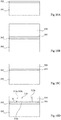
- FIGS. 3A, 3B, 4A, 4B, 5A, 5B , 6A, 6B, 7A, 7B, 8A, 8B , 9A and 9B schematically illustrate steps of a method of manufacturing an embodiment of a screen 400 provided with retroreflective microstructures, compatible with a system of the type described in connection with the figure 1 .
- the Figures 3A, 4A, 5A , 6A, 7A, 8A and 9A are perspective views, and the Figures 3B, 4B, 5B , 6B, 7B, 8B and 9B are sectional views along the BB plane of Figures 3A, 4A, 5A , 6A, 7A, 8A and 9A respectively.
- FIGS. 3A, 3B, 4A, 4B, 5A and 5B illustrate steps of manufacturing a primary mold 320 ( Figures 5A and 5B ) intended to be used during the manufacture of the screen 400 itself.
- the Figures 3A and 3B illustrate a step of arranging a mask 303 on the upper face of a substrate 301 in which it is desired to form the primary mold 320.
- the substrate 301 is for example glass, silicon, a thermoplastic polymer such as poly ( methyl methacrylate) or PMMA, or any other suitable material.
- the upper surface of the substrate 301 is preferably flat.
- the mask 303 comprises through openings 307 revealing portions of the upper surface of the substrate 301 to be etched in a subsequent step.
- the mask 303 is made of a material adapted to protect the unexposed portions of the substrate 301 during the subsequent etching step.
- the mask 303 is made of metal or resin.
- each opening 307 formed in the mask 303 comprises two side walls 308a and 308b substantially orthogonal to each other, joining to form an angle of approximately 90 degrees.
- Each opening 307 has, for example, seen from above, the shape of a convex pentagon.
- each opening 307 has, seen from above, the shape of a right isosceles triangle to which is juxtaposed a trapezium. The sides of the right triangle correspond to the side walls 308a and 308b, and the base of the right triangle is merged with a base (the large base in the example shown) of the trapezium.
- the openings 307 are for example all substantially identical and oriented substantially in the same manner.
- openings 307 In the example shown, only two openings 307 have been shown for the sake of simplification. In practice, a large number of openings 307 may be provided. For example, the openings 307 are regularly distributed over the entire upper surface of the substrate 301. The openings 307 are for example arranged in a matrix according to rows and columns.
- each cavity 311 comprises side walls substantially orthogonal to the upper face of the substrate 301 , and a bottom substantially parallel to the upper face of the substrate.
- each cavity comprises two side walls 312a and 312b substantially orthogonal to each other, substantially coinciding, seen from above, with the side walls 308a and 308b of the openings 307.
- side walls 312a and 312b and the bottom 312c of each cavity 311 meet at a same point S, and define a trirectangular trihedron or cube corner having the point S for vertex.
- the axis of symmetry or central axis of the vertex cube corner S forms, by construction, an angle of approximately 54.74 degrees with the upper face of the substrate 301.
- each cavity 311 the vertex cube corner S corresponds to a retroreflective microrefining of the future screen 400.
- the side wall 312d of each cavity 311 opposite the apex S (corresponding to the small base of the trapezium of the opening 307 in the example shown) is preferably relatively far from the vertex S, so as to define in the cavity 311 a clearance region facing the base of the cube corner.
- the cavity 311 has, in the direction of the bisector of the angle formed by the side walls 312a and 312b, a dimension between 1 and 1.5 times the depth of the cavity.
- the cavities 311 have for example a depth in the range of 20 to 500 microns and preferably in the range of 50 to 200 microns.
- the cavities 311 are for example formed by a deep ionic reactive etching process, generally referred to in the art by the acronym DRIE ("Deep Reactive Ion Etching").
- DRIE Deep Reactive Ion Etching
- Such a method has the advantage of making it possible to easily make cavities having substantially vertical lateral faces over relatively high depths, and a substantially horizontal bottom.
- Any other suitable etching process may however be used, for example a laser etching or an X-ray etching.
- the mask 303 (not shown on the Figures 4A and 4B ) is removed.
- the Figures 5A and 5B illustrate a step of forming trenches or recesses 314 with oblique or curved sides in the substrate 301, from the upper face of the substrate.
- the trenches 314 have a depth less than the thickness of the substrate 301.
- the trenches 314 pass through the clearance regions of the cavities 311, avoiding the cube-corner regions corresponding to the retroreflective microrefinements of the screen 400.
- the same trench 314 passes through several cavities 311.
- each trench 314 passes right through the substrate 301 in a direction of alignment of the cavities 311 not passing through the cube-corner portions of the cavities 311.
- a localized trench 314 is formed at each cavity 311, i.e. each trench 314 passes through a single cavity 311.
- the trenches 314 have a depth greater than or equal to that of the cavities 311, for example a depth of between 1 and 1.5 times the depth of the cavities 311.
- the trenches 314 preferably have a longitudinal plane of symmetry substantially orthogonal to the upper surface. of the substrate.
- the depth of the trenches 314, their width, and the inclination of their flanks, are chosen so as to eliminate all or part of the vertical walls of the cavities 311 which do not correspond to the cube-corner retroreflective regions of the screen 400.
- the trenches 314 are V trenches.
- V-trenches can for example be obtained by machining the substrate by means of a saw, or by etching.
- V trenches have for example an angular aperture of between 20 and 60 degrees, and preferably of the order of 50 degrees.
- the trenches 314 are trenches with curved flanks, for example trenches C.
- Such trenches may for example be made by etching.
- the trench prediction 314 facilitates a subsequent demolding step of a screen element 400 made from the mold 320.
- the trenches 314 are optional, and may in particular be omitted if it does not arise. no particular difficulty of demolding in this subsequent step.
- the angle of inclination Trench flanks 314 do not need to be precisely controlled because the trenches 314 serve only to facilitate demolding of the screen, but have no optical function in the final screen.
- the structure obtained after the steps 3A, 3B, 4A, 4B, 5A, 5B corresponds to the primary mold 320.
- the Figures 6A and 6B illustrate a step in which the structures of the upper surface of the primary mold 320 are replicated, by molding, on one face (the upper face in the example shown) of a film 351.
- the film 351 is made of a plastic material, for example of the polymethyl methacrylate type.
- the film 351 is made of a transparent material.
- the replication of the patterns of the primary mold 320 on one side of the film 351 passes through the formation, from the primary mold 320, of a secondary mold (not shown) having a shape complementary to that of the primary mold 320.
- the upper face of the film 351 are then obtained from the secondary mold, by thermoforming or by any other suitable molding technique.
- references 311, 312a, 312b, 312c, 312d, S and 314 used to designate elements of the structures of the upper face of the primary mold 320 will be used to designate the corresponding elements.
- the unstructured face of the film 351, namely its underside in the example shown, is preferably substantially flat.
- the Figures 7A and 7B illustrate a step of arranging a mask 353 on the upper face of the film 351.
- the mask 353 comprises through openings 355 revealing portions of the upper face of the film 351. More particularly, the openings 355 are arranged substantially opposite the vertex cube corners S corresponding to the retro-reflective microrefinements of the screen 400.
- the remainder of the upper surface of the film 351, and in particular the flat portions of the upper surface of the film 351 not occupied by the cavities 311 and the trenches 314, as well as the portions of the upper surface of the film 351 corresponding to the trenches 314 and cavity clearance regions 311, are covered by the mask 353.
- the Figures 8A and 8B illustrate the result of a deposition step, through the apertures 355 of the mask 353, of reflective metallizations 357 coating the side walls and the bottom of the cube-corner micro-cavities of the upper face of the film 351.
- the metallizations 357 are for example in aluminium.
- the metallizations 357 may be spray deposited through the openings of the mask.
- the metallizations 357 may overflow on the upper face of the film 351 slightly beyond the limit of the cube corners S vertex.
- each metallization 357 may have the shape of a substantially circular pastille in which is inscribed the corresponding right triangle, seen from above, at the cube-corner recess coated by the metallization 357.
- the mask 353 is removed.
- the Figures 9A and 9B illustrate a step of bonding a transparent coating film 359 to the upper face of the film 351.
- the faces of the film 359 are substantially planar.
- the coating film 359 and the transparent adhesive 361 have substantially the same refractive index as the film 351.
- the coating film 359 and the transparent adhesive layer 361 ensure a good transparency of the screen 400 outside the areas coated by the metallizations 357. assembly thus obtained forms the screen 400.
- the screen 400 has retroreflective portions regularly distributed over its entire surface, corresponding to the metallized cube corner structures of the film 351. Each The portion of the retroreflective screen is surrounded by a portion of transparent screen, so that the screen is partially retroreflective and partially transparent.
- the screen 400 is thus adapted to an operation of the type described in connection with the figure 1 (the upper face of the screen being turned towards the projector 105).
- the coverage rate of the screen 400 by the retroreflective portions is for example less than 50%, and preferably less than 20%.
- the incident rays are deflected by an angle which depends on the optical index of the film 359.
- the maximum efficiency in retroreflection of the cube corner the screen 400 is in principle obtained when the rays projected on these structures are parallel to the central axis of the corner cube corners S, that is to say when the rays propagating inside the screen are tilted about 54.74 degrees from the mid-plane of the screen.
- Such an inclination of the rays inside the screen can not generally be obtained in practice, this inclination being greater than the limit angle of refraction of the upper diopter of the screen.
- the refractive limit angle is about 42 degrees.
- the higher the angle of incidence of the light rays on the screen 400 the higher the reflection losses on the upper face of the screen 400 are important.
- analyzes have shown that, when the films 359 and 351 and the adhesive layer 361 have a refractive index of the order of 1.5, the maximum efficiency in retroreflection of the screen 400 is obtained for an angle of incidence (outside the screen) of the order of 60 degrees.
- the proposed structure provides good retroreflection efficiency at angles of incidence in the range of 30 to 80 degrees, and preferably in the range of 50 to 70 degrees.
- the screen 400 is well suited to the application to the projection of an image on a vehicle windshield.
- the screen 400 is relatively simple to implement, because the cube-corner microbreaks forming the retroreflective portions of the screen do not have oblique faces relative to the mean plane of the screen. 'screen.
- the faces of the cube-corner microbreaks of the screen 400 are substantially orthogonal or parallel to the mean plane of the screen.
- the cube corner micro-cavities can be obtained by means of a simple etching vertical sides from the upper surface of the substrate 301.
- the cube corner microrangements forming the retroreflective portions of the screen 400 are not necessarily aligned in rows and columns, but may have a random or semi-random arrangement on the surface of the screen, in particular to avoid possible diffractive phenomena that may occur at certain angles of incidence when the microbreaks have a regular disposition.
- the embodiments described are not limited to the exemplary method of producing the reflective metallizations 357 described in connection with the FIGS. 7A, 7B, 8A, 8B .
- the step of producing the mask 353 described in connection with the Figures 7A and 7B can be omitted. Instead, a conformal metal layer covering the entire upper surface of the structure of the Figures 6A and 6B can be realized. The deposited metal can then be removed at the upper planar regions of the structure (corresponding to the transparent areas of the screen), for example by mechanochemical polishing. During this step, only the portions of the metal layer coating the walls of the cavities 311, and, where appropriate, the trenches 314, are preserved, forming the reflective metallizations 357.
- the light source 105 is usually not placed exactly in the axis of the user's gaze.
- the screen 400 should preferably be adapted to diffuse the retroreflected light in a diffusion cone encompassing the pupils of the user, so that the user can see the image displayed by the projector.
- the inventors have found that the diffraction effects on the edges of microrenfoncements and / or the inevitable surface imperfections of the screen, may be sufficient to obtain the required diffusion effect.
- the described embodiments are not limited to the application to the projection of an image on a transparent surface.
- the embodiments described may have applications in various fields using retroreflective surfaces, not necessarily transparent, for example for signaling purposes.
- such a surface may have utility for ground signaling applications in the field of motor vehicle routes.
- the transparency is not sought, it will preferably seek to maximize the coverage rate of the screen by the retroreflective portions of cube corners.
- the material of the film 351 may be non-transparent.
- the coating film 359 and the intermediate adhesive layer 361 must be transparent to allow the incident light to reach the cube-corner metallizations 357 and then to emerge from the screen after reflection on the faces of the metallizations. Alternatively, the coating film 359 and the intermediate glue layer 361 may be omitted. On the other hand, if the transparency of the screen is not required, the reflective metallizations 357 are not necessarily located on the cube corner portions of the substrate 351, but can form a continuous layer made by conformal deposition, coating the entire upper surface of the substrate 351.
- film has been used to designate the elements 351 and 359 of the screen 400. This term must, however, be broadly understood, and notably includes elements similar to films such as leaves, plates, etc.
- FIGS. 10A, 10B, 10C and 10D are sectional views schematically illustrating an alternative embodiment of the method of FIGS. 3A, 3B, 4A, 4B, 5A, 5B , 6A, 6B, 7A, 7B, 8A, 8B and 9A, 9B .
- the process of FIGS. 10A, 10B, 10C and 10D differs from the process of FIGS. 3A, 3B, 4A, 4B, 5A, 5B , 6A, 6B, 7A, 7B, 8A, 8B and 9A, 9B essentially in the manufacturing steps of the primary mold used to make the retroreflective screen.
- the figure 10A illustrates an initial step in which is formed, on and in contact with the front face of a first substrate 501 having a front face (the upper face in the orientation of the figure 10A ) and a rear face (the lower face in the orientation of the figure 10A ), a layer 503 of a material such as the substrate 501 is selectively etchable with respect to the layer 503.
- the front face of the substrate 501 is preferably flat.
- the substrate 501 is made of silicon and the layer 503 is made of silicon oxide.
- the layer 503 is for example formed by oxidation of the upper surface of the substrate 501.
- the figure 10B illustrates a step subsequent to the formation of the layer 503, during which the first substrate 501 is transferred to a second substrate or support substrate 505, so that the front face of the layer 503, that is to say the face of the layer 503 opposite the substrate 501, is turned towards the substrate 505.
- the substrate 505 is a silicon substrate identical or similar to the substrate 501, and the substrate 505 is coated, on the side of its front side (the upper face in the orientation of the figure 10B ), a layer of silicon oxide 507 identical or similar to the layer 503.
- the front face of the layer 503 is brought into contact with the front face of the layer 507.
- the respective front faces of the silicon oxide layers 503 and 507 are surface-treated beforehand to obtain a molecular bonding of the two layers when they come into contact.
- the described embodiments are however not limited to this particular case.
- the support substrate 505 may not be of the same nature as the substrate 501.
- the support substrate 505 is not necessarily coated with a layer of the same nature as the layer 503. , the bonding of the substrates 501 and 505 can be achieved by a technique other than molecular bonding.
- the Figure 10C illustrates a step subsequent to the step of placing the substrate 501 on the substrate 505, during which the substrate 501 is thinned from its rear face (that is to say its upper face in the orientation of the Figure 10C ).
- the thinning comprises for example a step of grinding the rear face of the substrate 501, followed by a planarization step, for example a mechanochemical polishing. More generally, any other known thinning process may be used.
- the thinning may comprise a cleavage step, followed by a planarization step.
- a prior ion implantation step may be provided to define the cleavage zone. If the thickness of the substrate 501 remaining above the layer 503 at the end of the cleavage step is insufficient, a step of depositing or growing a layer of the substrate material on the rear face of the substrate 501 may be provided after the cleavage step.
- the rear face of the substrate 501 is preferably substantially flat and parallel to the front face of the substrate 501.
- the thickness of substrate 501 remaining above the layer 503 at the end of the thinning step is equal to the depth of the cube corner cavities or recesses 311 of the primary mold that we seek to achieve.
- the thickness of substrate 501 remaining above the layer 503 is in the range of 20 to 500 microns and preferably in the range of 50 to 200 microns.
- FIGS. 3A, 3B, 4A, 4B, 5A, 5B , 6A, 6B, 7A, 7B, 8A, 8B and 9A, 9B is then implemented identically or similarly to what has been described above, replacing the substrate 301 by the assembly formed by the thinned substrate 501, the layer 503, the support substrate 505 and the layer 507.
- the rear face of the thinned substrate 501 is substituted for the upper face of the substrate 301.
- the figure 10D illustrates the step of forming cavities or recesses 311 of the primary mold, extending substantially vertically in the substrate 501, from its rear face. This step corresponds to the step described above in relation to the Figures 4A and 4B .
- the etching process used to form the cavities 311 is chosen to etch the substrate selectively with respect to the material of the layer 503.
- the cavities 311 are made by deep ionic reactive etching (DRIE).
- the layer 503 forms an etch stop layer, that is to say that the etching of the cavities 311 is interrupted on the rear face of the layer 503.
- the bottom 312c of each cavity 311 is formed by the back side of layer 503.
- An advantage of the process of Figures 10A to 10D resides in the fact that the presence of the etch stop layer 503 ensures a good flatness of the bottom 312c cavities 311.
- the bottom 312c of each cavity 311 remains flat until vertex S of the cube corner, so that the right angle obtained between the bottom 312c and the side faces 312a, 312b of each cavity 311 is sharp (without rounding). This makes it possible to improve the retroreflective performance of the final screen compared with the method of the FIGS.
- FIGS. 11A, 11B, 11C, 11D, 11E , 11F and 11G are sectional views schematically illustrating another variant embodiment of the method of FIGS. 3A, 3B, 4A, 4B, 5A, 5B , 6A, 6B, 7A, 7B, 8A, 8B and 9A, 9B .
- FIG. 11A to 11G has similarities to the process of the Figures 10A to 10D and takes advantage of the presence of the etch stop layer 503 to form roughness on the bottom 312c of the cavities 311 of the primary mold, so as to introduce a controlled diffusion function of the light retroreflected by the screen, so as to that the user can see the image displayed by the projector even when the light source 105 is not placed exactly in the axis of the user's gaze.
- This controlled diffusion is particularly interesting in systems in which the projector is dissociated from the user, for example when the projector is secured to the vehicle and not the user himself.
- the Figures 11A and 11B illustrate an initial step of forming roughness on the front face of the substrate 501, before the deposition of the layer 503.
- a photoresist layer 601 figure 11A
- the desired roughness pattern is formed by a grayscale lithography step.
- Structures (not visible on the figure 11A ) of the resin layer 601 are then etched onto the upper face of the substrate 501 ( Figure 11B ).
- any other method for structuring the upper surface of the substrate 501 to obtain the function of desired broadcast can be used.
- Examples of roughness patterns for obtaining a controlled diffusion of light are for example described in the patent US8114248 .
- the roughnesses formed on the front face of the substrate 501 have dimensions greater than the longest wavelength of the light that one seeks to retroreflect.
- the figure 11C illustrates a step of forming the layer 503 on and in contact with the structured front face of the substrate 501.
- This step is for example identical or similar to what has been described in connection with the figure 10A .
- the layer 503 has on its rear face (that is to say, its lower face in the orientation of the figure 11C ) Structures complementary to those of the front face of the substrate 501. It will be noted that in the case where the layer 503 is formed by oxidation of the front face of the substrate 501, the roughnesses previously formed on the front face of the substrate 501 can be deformed by oxidation.
- the dimensioning of the roughnesses formed on the front face of the substrate 501 at the steps of Figures 11A and 11B can be achieved taking into account these deformations.
- the subsequent etching step of the cavities 311 of the primary mold is carried out by a selective etching process of the substrate 501 with respect to the layer 503, this etching step may nevertheless cause a deformation of the rear-end structure. of the layer 503. This deformation can be taken into account in the dimensioning of the roughnesses formed on the front face of the substrate 501 at the stages of the Figures 11A and 11B .
- the figure 11D illustrates a step of planarization of the front face (that is to say the upper face in the orientation of the figure 11D ) of the layer 503.
- the figure 11E illustrates a step subsequent to the deposition of the layer 503, during which the substrate 501 is transferred to a second substrate or support substrate 505, so that the front face of the layer 503, that is to say the face of the layer 503 opposite the substrate 501, is turned towards the substrate 505.
- This step is for example identical or similar to what has been described in connection with the figure 10B .
- the figure 11F illustrates a step subsequent to the step of transferring the substrate 501 to the substrate 505, during which the substrate 501 is thinned from its rear face. This step is for example identical or similar to what has been described in connection with the Figure 10C .
- FIGS. 3A, 3B, 4A, 4B, 5A, 5B , 6A, 6B, 7A, 7B, 8A, 8B and 9A, 9B is then implemented identically or similarly to what has been described above, replacing the substrate 301 by the assembly obtained at the end of the step of the figure 11F .
- the rear face of the thinned substrate 501 is substituted for the upper face of the substrate 301.
- the figure 11G illustrates the step of forming cavities or recesses 311 of the primary mold, extending substantially vertically in the substrate 501, from its rear face. This step is for example identical or similar to what has been described in connection with the figure 10D .
- An advantage of the process of Figures 11A to 11G is that it allows, relatively simply, to achieve, in the cube-corner areas of the cavities 311 of the primary mold 320, corresponding to the retroreflective portions of the screen 400, structures adapted to increase the opening of the cone of diffusion of retroreflected light.
- the step of thinning the substrate 501 by its rear face can be omitted if the thickness of the substrate 501 is already equal to the depth of the cavities or recesses cube corners 311 that we seek to achieve.
- the support substrate 505 on which the substrate 501 and the etch stop layer 503 is carried is intended to ensure the mechanical strength of the assembly from which the primary mold is formed.
- the support substrate 505 is necessary when the primary mold comprises demolding trenches 314 passing right through the substrate as has been described in connection with the Figures 5A and 5B .
- the trenches 314 being deeper than the cavities 311, the formation of the trenches 314 amounts to cutting the substrate 501 into disjoint strips. In the absence of the support substrate 505, these substrate strips 501 would disengage from one another.
Landscapes
- Engineering & Computer Science (AREA)
- Mechanical Engineering (AREA)
- Health & Medical Sciences (AREA)
- Manufacturing & Machinery (AREA)
- Ophthalmology & Optometry (AREA)
- Optical Elements Other Than Lenses (AREA)
- Moulds For Moulding Plastics Or The Like (AREA)
Applications Claiming Priority (1)
| Application Number | Priority Date | Filing Date | Title |
|---|---|---|---|
| FR1650226A FR3046682B1 (fr) | 2016-01-12 | 2016-01-12 | Procede de fabrication d'un ecran muni de microstructures retroreflechissantes |
Publications (2)
| Publication Number | Publication Date |
|---|---|
| EP3192645A1 true EP3192645A1 (de) | 2017-07-19 |
| EP3192645B1 EP3192645B1 (de) | 2018-06-06 |
Family
ID=55361873
Family Applications (1)
| Application Number | Title | Priority Date | Filing Date |
|---|---|---|---|
| EP17150779.1A Active EP3192645B1 (de) | 2016-01-12 | 2017-01-10 | Herstellungsverfahren eines bildschirms, der mit rückstrahlenden mikrostrukturen ausgestattet ist |
Country Status (3)
| Country | Link |
|---|---|
| US (1) | US10583585B2 (de) |
| EP (1) | EP3192645B1 (de) |
| FR (1) | FR3046682B1 (de) |
Cited By (1)
| Publication number | Priority date | Publication date | Assignee | Title |
|---|---|---|---|---|
| EP3764169A1 (de) * | 2019-07-10 | 2021-01-13 | Patek Philippe SA Genève | Verfahren zum abschnittsweisen satinieren einer uhrenkomponente aus silizium |
Families Citing this family (3)
| Publication number | Priority date | Publication date | Assignee | Title |
|---|---|---|---|---|
| WO2011060086A1 (en) * | 2009-11-12 | 2011-05-19 | 3M Innovative Properties Company | Irradiation marking of retroreflective sheeting |
| FR3103575B1 (fr) | 2019-11-27 | 2021-12-03 | Commissariat Energie Atomique | Ecran muni de microstructures rétroréfléchissantes |
| KR102905168B1 (ko) * | 2024-12-31 | 2025-12-29 | 주식회사 메스텍 | 재귀반사필름 금속금형 제작 방법 |
Citations (4)
| Publication number | Priority date | Publication date | Assignee | Title |
|---|---|---|---|---|
| US20040004765A1 (en) * | 2002-06-27 | 2004-01-08 | Ichiro Ihara | Corner cube array and method of making the corner cube array |
| JP2011191404A (ja) * | 2010-03-12 | 2011-09-29 | Stanley Electric Co Ltd | 2面コーナーリフレクタアレイ光学素子およびそれを用いた表示装置 |
| US8114248B2 (en) | 2007-01-03 | 2012-02-14 | Asahi Kasei Kabushiki Kaisha | Roll-to-roll method and system for micro-replication of a pattern of large relief three-dimensional microstructures |
| WO2015158999A1 (fr) | 2014-04-16 | 2015-10-22 | Commissariat A L'energie Atomique Et Aux Energies Alternatives | Systeme d'affichage d'une image sur un pare-brise |
Family Cites Families (2)
| Publication number | Priority date | Publication date | Assignee | Title |
|---|---|---|---|---|
| US6406638B1 (en) * | 2000-01-06 | 2002-06-18 | The Regents Of The University Of California | Method of forming vertical, hollow needles within a semiconductor substrate, and needles formed thereby |
| FR3040502B1 (fr) * | 2015-08-28 | 2018-02-16 | Commissariat A L'energie Atomique Et Aux Energies Alternatives | Ecran muni de microstructures retroreflechissantes |
-
2016
- 2016-01-12 FR FR1650226A patent/FR3046682B1/fr not_active Expired - Fee Related
-
2017
- 2017-01-10 EP EP17150779.1A patent/EP3192645B1/de active Active
- 2017-01-12 US US15/404,684 patent/US10583585B2/en active Active
Patent Citations (5)
| Publication number | Priority date | Publication date | Assignee | Title |
|---|---|---|---|---|
| US20040004765A1 (en) * | 2002-06-27 | 2004-01-08 | Ichiro Ihara | Corner cube array and method of making the corner cube array |
| US8114248B2 (en) | 2007-01-03 | 2012-02-14 | Asahi Kasei Kabushiki Kaisha | Roll-to-roll method and system for micro-replication of a pattern of large relief three-dimensional microstructures |
| JP2011191404A (ja) * | 2010-03-12 | 2011-09-29 | Stanley Electric Co Ltd | 2面コーナーリフレクタアレイ光学素子およびそれを用いた表示装置 |
| WO2015158999A1 (fr) | 2014-04-16 | 2015-10-22 | Commissariat A L'energie Atomique Et Aux Energies Alternatives | Systeme d'affichage d'une image sur un pare-brise |
| FR3020149A1 (fr) | 2014-04-16 | 2015-10-23 | Commissariat Energie Atomique | Systeme d'affichage d'une image sur un pare-brise |
Cited By (1)
| Publication number | Priority date | Publication date | Assignee | Title |
|---|---|---|---|---|
| EP3764169A1 (de) * | 2019-07-10 | 2021-01-13 | Patek Philippe SA Genève | Verfahren zum abschnittsweisen satinieren einer uhrenkomponente aus silizium |
Also Published As
| Publication number | Publication date |
|---|---|
| FR3046682B1 (fr) | 2018-02-16 |
| US20170197338A1 (en) | 2017-07-13 |
| US10583585B2 (en) | 2020-03-10 |
| FR3046682A1 (fr) | 2017-07-14 |
| EP3192645B1 (de) | 2018-06-06 |
Similar Documents
| Publication | Publication Date | Title |
|---|---|---|
| EP3192645B1 (de) | Herstellungsverfahren eines bildschirms, der mit rückstrahlenden mikrostrukturen ausgestattet ist | |
| EP3203316B1 (de) | Anzeigesystem eines bildes auf einer windschutzscheibe | |
| EP3526965B1 (de) | System zur herstellung einer schwebenden bildes | |
| EP3521879A1 (de) | Photonischer chip mit integrierter kollimationsstruktur | |
| EP3607585B1 (de) | Vorrichtung und verfahren zur multispektralen bildgebung im infrarotbereich | |
| EP3141952B1 (de) | Bildschirm, der mit rückstrahlenden mikrostrukturen ausgestattet ist | |
| FR2981460A1 (fr) | Procede de realisation d'un dispositif optique refractif ou diffractif | |
| EP4269182A1 (de) | Modulare schwimmende optische 3d-textur | |
| EP3855068A1 (de) | Vorrichtung zur verteilten lichtprojektion | |
| EP2226678A1 (de) | Verfahren zur Herstellung einer Nanoimprintform | |
| EP4170426B1 (de) | Schirm mit reflektierenden mikrostrukturen | |
| WO2021063979A1 (fr) | Système optique | |
| EP4016055A1 (de) | Optische komponente für eine interferometrische atr-bildgebungsvorrichtung | |
| EP3798695A1 (de) | Diffuse struktur für lichtquelle | |
| WO2016162632A1 (fr) | Système d'affichage d'une image flottante | |
| WO2025252831A1 (fr) | Module réfléchissant rouge pour pièce automobile, et système associé | |
| EP4733818A1 (de) | Optische komponente, die teilweise transparent und teilweise retroreflektierend ist, mit plansymmetrischer ablenkung | |
| FR3149426A3 (fr) | Module optique pour un dispositif lumineux d'un véhicule automobile | |
| EP2808734B1 (de) | Bildschirm und Vorrichtung zur Rückprojektionsanzeige | |
| FR3101626A1 (fr) | Procédé d'alignement | |
| FR3057677A1 (fr) | Procede de fabrication d'un guide d'onde | |
| FR3057675A1 (fr) | Procede de fabrication d'un guide d'onde |
Legal Events
| Date | Code | Title | Description |
|---|---|---|---|
| PUAI | Public reference made under article 153(3) epc to a published international application that has entered the european phase |
Free format text: ORIGINAL CODE: 0009012 |
|
| STAA | Information on the status of an ep patent application or granted ep patent |
Free format text: STATUS: REQUEST FOR EXAMINATION WAS MADE |
|
| 17P | Request for examination filed |
Effective date: 20170110 |
|
| AK | Designated contracting states |
Kind code of ref document: A1 Designated state(s): AL AT BE BG CH CY CZ DE DK EE ES FI FR GB GR HR HU IE IS IT LI LT LU LV MC MK MT NL NO PL PT RO RS SE SI SK SM TR |
|
| AX | Request for extension of the european patent |
Extension state: BA ME |
|
| GRAP | Despatch of communication of intention to grant a patent |
Free format text: ORIGINAL CODE: EPIDOSNIGR1 |
|
| STAA | Information on the status of an ep patent application or granted ep patent |
Free format text: STATUS: GRANT OF PATENT IS INTENDED |
|
| INTG | Intention to grant announced |
Effective date: 20180103 |
|
| GRAS | Grant fee paid |
Free format text: ORIGINAL CODE: EPIDOSNIGR3 |
|
| GRAA | (expected) grant |
Free format text: ORIGINAL CODE: 0009210 |
|
| STAA | Information on the status of an ep patent application or granted ep patent |
Free format text: STATUS: THE PATENT HAS BEEN GRANTED |
|
| AK | Designated contracting states |
Kind code of ref document: B1 Designated state(s): AL AT BE BG CH CY CZ DE DK EE ES FI FR GB GR HR HU IE IS IT LI LT LU LV MC MK MT NL NO PL PT RO RS SE SI SK SM TR |
|
| REG | Reference to a national code |
Ref country code: GB Ref legal event code: FG4D Free format text: NOT ENGLISH |
|
| REG | Reference to a national code |
Ref country code: CH Ref legal event code: EP Ref country code: AT Ref legal event code: REF Ref document number: 1005589 Country of ref document: AT Kind code of ref document: T Effective date: 20180615 |
|
| REG | Reference to a national code |
Ref country code: IE Ref legal event code: FG4D Free format text: LANGUAGE OF EP DOCUMENT: FRENCH |
|
| REG | Reference to a national code |
Ref country code: DE Ref legal event code: R096 Ref document number: 602017000080 Country of ref document: DE |
|
| REG | Reference to a national code |
Ref country code: NL Ref legal event code: MP Effective date: 20180606 |
|
| REG | Reference to a national code |
Ref country code: LT Ref legal event code: MG4D |
|
| PG25 | Lapsed in a contracting state [announced via postgrant information from national office to epo] |
Ref country code: NO Free format text: LAPSE BECAUSE OF FAILURE TO SUBMIT A TRANSLATION OF THE DESCRIPTION OR TO PAY THE FEE WITHIN THE PRESCRIBED TIME-LIMIT Effective date: 20180906 Ref country code: FI Free format text: LAPSE BECAUSE OF FAILURE TO SUBMIT A TRANSLATION OF THE DESCRIPTION OR TO PAY THE FEE WITHIN THE PRESCRIBED TIME-LIMIT Effective date: 20180606 Ref country code: ES Free format text: LAPSE BECAUSE OF FAILURE TO SUBMIT A TRANSLATION OF THE DESCRIPTION OR TO PAY THE FEE WITHIN THE PRESCRIBED TIME-LIMIT Effective date: 20180606 Ref country code: BG Free format text: LAPSE BECAUSE OF FAILURE TO SUBMIT A TRANSLATION OF THE DESCRIPTION OR TO PAY THE FEE WITHIN THE PRESCRIBED TIME-LIMIT Effective date: 20180906 Ref country code: CY Free format text: LAPSE BECAUSE OF FAILURE TO SUBMIT A TRANSLATION OF THE DESCRIPTION OR TO PAY THE FEE WITHIN THE PRESCRIBED TIME-LIMIT Effective date: 20180606 Ref country code: LT Free format text: LAPSE BECAUSE OF FAILURE TO SUBMIT A TRANSLATION OF THE DESCRIPTION OR TO PAY THE FEE WITHIN THE PRESCRIBED TIME-LIMIT Effective date: 20180606 Ref country code: SE Free format text: LAPSE BECAUSE OF FAILURE TO SUBMIT A TRANSLATION OF THE DESCRIPTION OR TO PAY THE FEE WITHIN THE PRESCRIBED TIME-LIMIT Effective date: 20180606 |
|
| PG25 | Lapsed in a contracting state [announced via postgrant information from national office to epo] |
Ref country code: LV Free format text: LAPSE BECAUSE OF FAILURE TO SUBMIT A TRANSLATION OF THE DESCRIPTION OR TO PAY THE FEE WITHIN THE PRESCRIBED TIME-LIMIT Effective date: 20180606 Ref country code: GR Free format text: LAPSE BECAUSE OF FAILURE TO SUBMIT A TRANSLATION OF THE DESCRIPTION OR TO PAY THE FEE WITHIN THE PRESCRIBED TIME-LIMIT Effective date: 20180907 Ref country code: HR Free format text: LAPSE BECAUSE OF FAILURE TO SUBMIT A TRANSLATION OF THE DESCRIPTION OR TO PAY THE FEE WITHIN THE PRESCRIBED TIME-LIMIT Effective date: 20180606 Ref country code: RS Free format text: LAPSE BECAUSE OF FAILURE TO SUBMIT A TRANSLATION OF THE DESCRIPTION OR TO PAY THE FEE WITHIN THE PRESCRIBED TIME-LIMIT Effective date: 20180606 |
|
| REG | Reference to a national code |
Ref country code: AT Ref legal event code: MK05 Ref document number: 1005589 Country of ref document: AT Kind code of ref document: T Effective date: 20180606 |
|
| PG25 | Lapsed in a contracting state [announced via postgrant information from national office to epo] |
Ref country code: NL Free format text: LAPSE BECAUSE OF FAILURE TO SUBMIT A TRANSLATION OF THE DESCRIPTION OR TO PAY THE FEE WITHIN THE PRESCRIBED TIME-LIMIT Effective date: 20180606 |
|
| PG25 | Lapsed in a contracting state [announced via postgrant information from national office to epo] |
Ref country code: RO Free format text: LAPSE BECAUSE OF FAILURE TO SUBMIT A TRANSLATION OF THE DESCRIPTION OR TO PAY THE FEE WITHIN THE PRESCRIBED TIME-LIMIT Effective date: 20180606 Ref country code: CZ Free format text: LAPSE BECAUSE OF FAILURE TO SUBMIT A TRANSLATION OF THE DESCRIPTION OR TO PAY THE FEE WITHIN THE PRESCRIBED TIME-LIMIT Effective date: 20180606 Ref country code: EE Free format text: LAPSE BECAUSE OF FAILURE TO SUBMIT A TRANSLATION OF THE DESCRIPTION OR TO PAY THE FEE WITHIN THE PRESCRIBED TIME-LIMIT Effective date: 20180606 Ref country code: AT Free format text: LAPSE BECAUSE OF FAILURE TO SUBMIT A TRANSLATION OF THE DESCRIPTION OR TO PAY THE FEE WITHIN THE PRESCRIBED TIME-LIMIT Effective date: 20180606 Ref country code: IS Free format text: LAPSE BECAUSE OF FAILURE TO SUBMIT A TRANSLATION OF THE DESCRIPTION OR TO PAY THE FEE WITHIN THE PRESCRIBED TIME-LIMIT Effective date: 20181006 Ref country code: PL Free format text: LAPSE BECAUSE OF FAILURE TO SUBMIT A TRANSLATION OF THE DESCRIPTION OR TO PAY THE FEE WITHIN THE PRESCRIBED TIME-LIMIT Effective date: 20180606 Ref country code: SK Free format text: LAPSE BECAUSE OF FAILURE TO SUBMIT A TRANSLATION OF THE DESCRIPTION OR TO PAY THE FEE WITHIN THE PRESCRIBED TIME-LIMIT Effective date: 20180606 |
|
| PG25 | Lapsed in a contracting state [announced via postgrant information from national office to epo] |
Ref country code: IT Free format text: LAPSE BECAUSE OF FAILURE TO SUBMIT A TRANSLATION OF THE DESCRIPTION OR TO PAY THE FEE WITHIN THE PRESCRIBED TIME-LIMIT Effective date: 20180606 Ref country code: SM Free format text: LAPSE BECAUSE OF FAILURE TO SUBMIT A TRANSLATION OF THE DESCRIPTION OR TO PAY THE FEE WITHIN THE PRESCRIBED TIME-LIMIT Effective date: 20180606 |
|
| REG | Reference to a national code |
Ref country code: DE Ref legal event code: R097 Ref document number: 602017000080 Country of ref document: DE |
|
| PLBE | No opposition filed within time limit |
Free format text: ORIGINAL CODE: 0009261 |
|
| STAA | Information on the status of an ep patent application or granted ep patent |
Free format text: STATUS: NO OPPOSITION FILED WITHIN TIME LIMIT |
|
| 26N | No opposition filed |
Effective date: 20190307 |
|
| PG25 | Lapsed in a contracting state [announced via postgrant information from national office to epo] |
Ref country code: DK Free format text: LAPSE BECAUSE OF FAILURE TO SUBMIT A TRANSLATION OF THE DESCRIPTION OR TO PAY THE FEE WITHIN THE PRESCRIBED TIME-LIMIT Effective date: 20180606 |
|
| PG25 | Lapsed in a contracting state [announced via postgrant information from national office to epo] |
Ref country code: MC Free format text: LAPSE BECAUSE OF FAILURE TO SUBMIT A TRANSLATION OF THE DESCRIPTION OR TO PAY THE FEE WITHIN THE PRESCRIBED TIME-LIMIT Effective date: 20180606 |
|
| PG25 | Lapsed in a contracting state [announced via postgrant information from national office to epo] |
Ref country code: LU Free format text: LAPSE BECAUSE OF NON-PAYMENT OF DUE FEES Effective date: 20190110 |
|
| REG | Reference to a national code |
Ref country code: BE Ref legal event code: MM Effective date: 20190131 |
|
| REG | Reference to a national code |
Ref country code: IE Ref legal event code: MM4A |
|
| PG25 | Lapsed in a contracting state [announced via postgrant information from national office to epo] |
Ref country code: BE Free format text: LAPSE BECAUSE OF NON-PAYMENT OF DUE FEES Effective date: 20190131 Ref country code: AL Free format text: LAPSE BECAUSE OF FAILURE TO SUBMIT A TRANSLATION OF THE DESCRIPTION OR TO PAY THE FEE WITHIN THE PRESCRIBED TIME-LIMIT Effective date: 20180606 |
|
| PG25 | Lapsed in a contracting state [announced via postgrant information from national office to epo] |
Ref country code: IE Free format text: LAPSE BECAUSE OF NON-PAYMENT OF DUE FEES Effective date: 20190110 |
|
| PG25 | Lapsed in a contracting state [announced via postgrant information from national office to epo] |
Ref country code: TR Free format text: LAPSE BECAUSE OF FAILURE TO SUBMIT A TRANSLATION OF THE DESCRIPTION OR TO PAY THE FEE WITHIN THE PRESCRIBED TIME-LIMIT Effective date: 20180606 |
|
| PG25 | Lapsed in a contracting state [announced via postgrant information from national office to epo] |
Ref country code: MT Free format text: LAPSE BECAUSE OF FAILURE TO SUBMIT A TRANSLATION OF THE DESCRIPTION OR TO PAY THE FEE WITHIN THE PRESCRIBED TIME-LIMIT Effective date: 20180606 Ref country code: PT Free format text: LAPSE BECAUSE OF FAILURE TO SUBMIT A TRANSLATION OF THE DESCRIPTION OR TO PAY THE FEE WITHIN THE PRESCRIBED TIME-LIMIT Effective date: 20181008 |
|
| REG | Reference to a national code |
Ref country code: CH Ref legal event code: PL |
|
| PG25 | Lapsed in a contracting state [announced via postgrant information from national office to epo] |
Ref country code: LI Free format text: LAPSE BECAUSE OF NON-PAYMENT OF DUE FEES Effective date: 20200131 Ref country code: CH Free format text: LAPSE BECAUSE OF NON-PAYMENT OF DUE FEES Effective date: 20200131 |
|
| PG25 | Lapsed in a contracting state [announced via postgrant information from national office to epo] |
Ref country code: HU Free format text: LAPSE BECAUSE OF FAILURE TO SUBMIT A TRANSLATION OF THE DESCRIPTION OR TO PAY THE FEE WITHIN THE PRESCRIBED TIME-LIMIT; INVALID AB INITIO Effective date: 20170110 |
|
| PG25 | Lapsed in a contracting state [announced via postgrant information from national office to epo] |
Ref country code: SI Free format text: LAPSE BECAUSE OF FAILURE TO SUBMIT A TRANSLATION OF THE DESCRIPTION OR TO PAY THE FEE WITHIN THE PRESCRIBED TIME-LIMIT Effective date: 20180606 |
|
| PG25 | Lapsed in a contracting state [announced via postgrant information from national office to epo] |
Ref country code: MK Free format text: LAPSE BECAUSE OF FAILURE TO SUBMIT A TRANSLATION OF THE DESCRIPTION OR TO PAY THE FEE WITHIN THE PRESCRIBED TIME-LIMIT Effective date: 20180606 |
|
| PGFP | Annual fee paid to national office [announced via postgrant information from national office to epo] |
Ref country code: GB Payment date: 20260121 Year of fee payment: 10 |
|
| PGFP | Annual fee paid to national office [announced via postgrant information from national office to epo] |
Ref country code: DE Payment date: 20260120 Year of fee payment: 10 |
|
| PGFP | Annual fee paid to national office [announced via postgrant information from national office to epo] |
Ref country code: FR Payment date: 20260128 Year of fee payment: 10 |