EP3219002B1 - Introducing jitter to a switching frequency by way of modulating current limit - Google Patents
Introducing jitter to a switching frequency by way of modulating current limit Download PDFInfo
- Publication number
- EP3219002B1 EP3219002B1 EP15797547.5A EP15797547A EP3219002B1 EP 3219002 B1 EP3219002 B1 EP 3219002B1 EP 15797547 A EP15797547 A EP 15797547A EP 3219002 B1 EP3219002 B1 EP 3219002B1
- Authority
- EP
- European Patent Office
- Prior art keywords
- signal
- controller
- current limit
- jitter
- power switch
- Prior art date
- Legal status (The legal status is an assumption and is not a legal conclusion. Google has not performed a legal analysis and makes no representation as to the accuracy of the status listed.)
- Active
Links
Images

Classifications
-
- H—ELECTRICITY
- H02—GENERATION; CONVERSION OR DISTRIBUTION OF ELECTRIC POWER
- H02M—APPARATUS FOR CONVERSION BETWEEN AC AND AC, BETWEEN AC AND DC, OR BETWEEN DC AND DC, AND FOR USE WITH MAINS OR SIMILAR POWER SUPPLY SYSTEMS; CONVERSION OF DC OR AC INPUT POWER INTO SURGE OUTPUT POWER; CONTROL OR REGULATION THEREOF
- H02M1/00—Details of apparatus for conversion
- H02M1/44—Circuits or arrangements for compensating for electromagnetic interference in converters or inverters
-
- H—ELECTRICITY
- H02—GENERATION; CONVERSION OR DISTRIBUTION OF ELECTRIC POWER
- H02M—APPARATUS FOR CONVERSION BETWEEN AC AND AC, BETWEEN AC AND DC, OR BETWEEN DC AND DC, AND FOR USE WITH MAINS OR SIMILAR POWER SUPPLY SYSTEMS; CONVERSION OF DC OR AC INPUT POWER INTO SURGE OUTPUT POWER; CONTROL OR REGULATION THEREOF
- H02M3/00—Conversion of DC power input into DC power output
- H02M3/22—Conversion of DC power input into DC power output with intermediate conversion into AC
- H02M3/24—Conversion of DC power input into DC power output with intermediate conversion into AC by static converters
- H02M3/28—Conversion of DC power input into DC power output with intermediate conversion into AC by static converters using discharge tubes with control electrode or semiconductor devices with control electrode to produce the intermediate AC
- H02M3/325—Conversion of DC power input into DC power output with intermediate conversion into AC by static converters using discharge tubes with control electrode or semiconductor devices with control electrode to produce the intermediate AC using devices of a triode or a transistor type requiring continuous application of a control signal
- H02M3/335—Conversion of DC power input into DC power output with intermediate conversion into AC by static converters using discharge tubes with control electrode or semiconductor devices with control electrode to produce the intermediate AC using devices of a triode or a transistor type requiring continuous application of a control signal using semiconductor devices only
- H02M3/33507—Conversion of DC power input into DC power output with intermediate conversion into AC by static converters using discharge tubes with control electrode or semiconductor devices with control electrode to produce the intermediate AC using devices of a triode or a transistor type requiring continuous application of a control signal using semiconductor devices only with automatic control of the output voltage or current, e.g. flyback converters
Definitions
- the present invention relates generally to controlling a power converter. More specifically, examples of the present invention are related to modulating a current limit signal to introduce jitter to the switching frequency of a switch mode power converter under varying load conditions.
- Switched mode power converters are commonly used due to their high efficiency, small size, and low weight to power many of today's electronics.
- Conventional wall sockets provide a high voltage alternating current.
- ac high voltage alternating current
- dc direct current
- a switch is turned ON and OFF to provide the desired output by varying the duty cycle (typically the ratio of the on time of the switch to the total switching period), varying the switching frequency, or varying the number of on/off pulses per unit time of the switch in a switched mode power converter.
- a switched mode power supply may emit too much EMI to meet safety regulation standards. Specifically for a power supply switching at a constant frequency, large levels of interference appearing on the fundamental/harmonics and related spurs may exceed the levels allowed by the EMI mask.
- US 2011/0110126 describes a controller for use in a power supply that includes a drive signal generator, a jitter signal generator and a compensator signal generator.
- the drive signal generator is coupled to output a drive signal having a switching period and a duty ratio to control switching of a switch that is to be coupled to the controller.
- the jitter signal generator is coupled to provide a jitter signal, where the switching period of the drive signal varies in response to the jitter signal.
- the compensator signal generator is coupled to provide a compensator signal responsive to the jitter signal, where the duty ratio of the drive signal is varied in response to the compensator signal.
- One way to reduce EMI interference appearing on the fundamental/harmonics in a switched mode power supply is to spread the energy out to other frequencies by varying the switching frequency, aka frequency jitter.
- Examples in accordance with the teachings of the present invention describe how the switching frequency can be jittered by perturbing the current limit in each switching cycle.
- Another benefit of the disclosed examples is to reduce audio noise by perturbing the current limit in each switching cycle.
- the equation P k ⁇ f ⁇ LI ⁇ 2 (k a constant, L is a fixed inductance, I is a fixed current limit, and f is a fixed switching frequency), describes how to keep the output power of a power converter constant. If however the current limit is varied, but the power is maintained to be constant by a feedback loop, f will be forced to vary to compensate for the change in I.
- jittering of the switching frequency can be achieved in accordance with the teachings of the present invention without the use of a variable frequency oscillator.
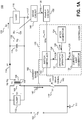
- FIG. 1A is a block diagram illustrating an example power converter with a modulated current limit signal to introduce jitter in a switching frequency in accordance with the teachings of the present invention.
- the illustrated example of power converter 100 includes an energy transfer element T1 104, a primary winding 106 of the energy transfer element T1 104, a secondary winding 108 of the energy transfer element T1 104, a power switch S1 110, an input return 111, a clamp circuit 112, a rectifier D1 114 (also referred to as an output diode D1), an output capacitor C1 116, an output return 117, a sense circuit 146, an enable circuit 122 and a controller 120.
- a rectifier D1 114 also referred to as an output diode D1
- an output capacitor C1 116 an output return 117
- a sense circuit 146 an enable circuit 122 and a controller 120.
- FIG.1A Also shown in FIG.1A are an input voltage V IN 102, an output quantity U O 134, an output voltage V O 130, an output current I O 133, a feedback signal U FB 136, a current sense signal 150, a drive signal 148, and switch current I D 140.
- the power converter 100 is shown as having a flyback topology for explanation purposes. It is appreciated that other known topologies and configurations of power converters may also benefit from the teachings of the present invention.
- the power converter 100 provides output power to a load 118 from an unregulated input V IN 102.
- the input V IN 102 is coupled to the energy transfer element T1 104.
- Power converter 100 uses the energy transfer element T1 104 to transfer energy from the primary winding 106 to the secondary winding 108.
- NP and NS represent the number of turns for the primary winding 106 and secondary winding 108, respectively.
- primary winding 106 may be considered an input winding
- secondary winding 108 may be considered an output winding.
- the primary winding 106 is further coupled to power switch S1 110, which is then further coupled to the input return 111.
- the clamp circuit 112 is coupled across the primary winding 106 of the energy transfer element T1 104.
- the secondary winding 108 of the energy transfer element T1 104 is coupled to the rectifier D1 114.
- the rectifier D1 114 is exemplified as a diode and the secondary winding 108 is coupled to the anode of the diode.
- Both the output capacitor C1 116 and the load 118 are coupled to the rectifier D1 114.
- both the output capacitor C1 116 and the load 118 are coupled to the cathode of the diode.
- An output is provided to the load 118 and may be provided as either an output voltage V O 130, output current I O 133, or a combination of the two.
- input voltage V IN 102 is positive with respect to input return 111
- output voltage V O 130 is positive with respect to output return 117.
- the example of FIG. 1A shows galvanic isolation between the input return 111 and the output return 117. In other words, a dc voltage applied between input return 111 and output return 117 will produce substantially zero current. Therefore, circuits electrically coupled to the primary winding 106 are galvanically isolated from circuits electrically coupled to the secondary winding 108.
- the power converter 100 further comprises circuitry to regulate the output, which is exemplified as output quantity U O 134.
- a sense circuit 146 is coupled to an enable circuit 122.
- the sense circuit 146 outputs a feedback signal U FB 136, which is representative of the output quantity U O 134.
- the current sense signal 150 may be representative of the drain current I D 140 in power switch S1 110.
- the switch controller 142 provides a drive signal 148 to the power switch S1 110 to control various switching parameters. Examples of such parameters may include switching frequency, switching period, duty cycle, or respective on and off times of the power switch S1 110.
- the clamp circuit 112 is coupled to the primary winding 106 of the energy transfer element T1 104 to limit the maximum voltage on the power switch S1 110.
- Power switch S1 110 is opened and closed in response to the drive signal 148 received from the controller 120. It is generally understood that a switch that is closed may conduct current and is considered ON, while a switch that is open cannot conduct current and is considered OFF.
- power switch S1 110 controls a drain current I D 140 in response to controller 120 to meet a specified performance of the power converter 100.
- the power switch S1 110 may be a transistor.
- the controller 120 comprises of a switch controller 142, an arithmetic operator 141, jitter generator 124, and a current limit generator 132.
- the switch controller 142 is coupled to receive the enable signal U EN 144 from the enable circuit 122.
- the drive signal 148 turns ON the power switch S1 110 in response to the enable signal U EN 144.
- the jitter generator 124 is coupled to provide a jitter signal U JTR 126 to the arithmetic operator.
- the jitter generator 124 may also be referred to as the jitter modulator.
- the current limit generator 132 generates a current limit signal U ILIM 128.
- the current limit generator 132 can be referred to as the control modulator.
- the arithmetic operator 141 is coupled to receive the jitter signal U JTR 126 and current limit signal U ILIM 128, and output a modulated current limit signal U JLIM 138 to the switch controller 142.
- the controller 120 also receives the current sense signal 150, which relays the sensed drain current I D 140 of the power switch S1 110.
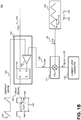
- FIG. 1B is a block diagram that further illustrates an example controller from FIG. 1A .
- Controller 120 comprises of a switch controller 142, an arithmetic operator 141, a jitter generator 124, and a current limit generator 132.
- Switch controller 142 comprises of a latch 166, and a comparator 168.
- Latch 166 is coupled to receive the enable signal U EN 144.
- the enable signal U EN 144 sets the drive signal 148 for power switch S1 110 for an ON period T ON 158.
- Comparator 168 is coupled to receive the current sense signal 150 at the non-inverting input, and the modulated current signal U JLIM 138 at the inverting input.
- the current sense signal is representative of the drain current I D 140 of the power switch S1 110. If the current sense signal is greater than the modulated current limit, latch 166 is reset, thereby turning OFF the power switch S1 110 for an OFF period T OFF 156.
- the switching period T S 154 comprises of the ON period T ON 158 and OFF period T OFF 156.
- the switching period T S 154 is adjusted every switching cycle such that energy is spread out across different frequencies, which in turn reduces the audio noise.
- the Jitter generator 124 generates a jitter signal U JTR 126.
- the jitter U JTR 126 signal may be a sawtooth waveform.
- the jitter signal U JTR 126 may be a traiangular waveform.
- the jitter signal U JTR 126 may be a stepped or stepladder waveform.
- the jitter signal U JTR 126 may be any waveform.
- the jitter signal U JTR 126 may have a modulation period T M 152. The modulation period T M 152 of the jitter signal U JTR 126 may be greater than the switching period T S 154.
- the arithmetic operator 141 is coupled to receive the current limit signal U ILIM 128 and the jitter signal U JTR 126.
- the arithmetic operator 141 is a multiplier 143.
- the arithmetic operator 141 can be another mathematical operator or multiple mathematical operators.
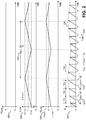
- FIG. 2 is an example timing diagram illustrating a process of the jitter generator and the current limit generator.
- the first timing diagram illustrates the current limit signal 228 generated by the current limit generator shown in FIG. 1A and FIG. IB.
- current limit signal U ILIM 228 is a constant value A.
- the second timing diagram illustrates the jitter signal U JTR 226 generated by the jitter generator shown in FIG. 1A and FIG. IB.
- the jitter signal is a triangular waveform with a peak value of (1+x), and a bottom value of (1-x).
- the value of x is between 0 and 1.
- a fractional value could be used for the value of x.
- the jitter signal U JTR 226 is a triangular waveform in this example, the jitter signal U JTR 226 may be represented by any variation of waveforms as stated previously.
- FIG. 2 Also shown in FIG. 2 is the output waveform of modulated current signal U JLIM 238 generated by the arithmetic operator in FIG. 1A and FIG.1B based on the current limit signal U ILIM 228 and jitter signal U JTR 226.
- the value of the modulated current signal U JLIM 238 varies from a peak value of (1+x)A to a bottom value of (1-x)A.
- the modulated current signal U JLIM 238 sets the maximum drain current I D 240, represented by waveform 238 for the switching cycle. Once the current limit is reached, the power switch is switched OFF for an OFF period T OFF 270.
- the fourth timing diagram illustrates the drain current 240 represented by the triangular waveforms.
- the dashed line waveform 238 superimposed on top of the drain current I D 240 sets the current limit as generated by the third timing diagram.
- the fourth timing diagram illustrates a first ON period T ON1 272 and a second ON period T ON 273.
- the fourth timing diagram further illustrates switching periods of T S1 , T S2 , T S3 , and T S4 where the values of these switching periods can vary. In this example, the values of T S1 , T S2 , T S3 , and T S4 are not equivalent and can vary.
- the values of the ON period T ON1 272 and ON period T ON2 273 may vary in this example, but it should be appreciated that the ON period of T ON1 272 and ON period T ON2 273 may also be equivalent. In other implementations, the values of the OFF period T OFF 270 can vary as well while the values of the ON period T ON 270 may remain the same.
- FIG. 2 shows the modulated current limit signal U JLIM 238 increasing then decreasing within the jitter generator period, it should be appreciated that modulated current limit signal U JLIM 238 may increase and decrease several times within the period of jitter generator then repeat for the next period of the jitter generator.
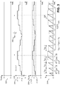
- FIG. 3 is another example timing diagram illustrating a process of the jitter generator and the current limit generator.
- the current limit generator generates a current limit signal U ILIM 328 of a constant value A.
- the jitter generator generates a jitter signal U JTR 326, in a stepladder waveform with a peak value of (1+x), and a bottom value of (1-x).
- the stepladder waveform may be one example of a digitally implemented triangular waveform.
- the value of x is between 0 and 1. A fractional value could be used for x.
- the arithmetic operator outputs a signal modulated current limit signal U JLIM 338 based on the current limit signal U ILIM 328 and jitter signal U JTR 326.
- the modulated current limit signal U JLIM 338 affects the drain current I D 340 by setting the maximum drain current, represented by the dashed line 338 above the drain current I D 340.
- the drain current I D 340 is represented by the triangular waveform.
- T S1 , T S2 , T S3 , and T S4 are not equivalent and can vary.
- the values of the ON period T ON1 372 and ON period T ON2 373 may vary in this example, but it should be appreciated that the ON period of T ON1 372 and ON period T ON2 373 may also be equivalent.
- the values of the OFF period T OFF 370 can vary as well while the values of the ON period T ON 370 may remain the same.
- the modulated current limit signal U JLIM 338 may increase and decrease several times within the jitter generator period then repeat for the next period of the jitter generator.
- FIG. 4 is another example timing diagram illustrating a process of the jitter generator and the current limit generator.
- the current limit generator generates a current limit signal U ILIM 428, represented by the value A that varies.
- the current limit signal U ILIM 428 may start each cycle at a first value and the decrease during the ON time within each switching cycle.
- the jitter generator generates a signal U JTR 426, which is a triangular waveform with a peak value of (1+x), and a bottom value of (1-x).
- the value of x is between 0 and 1.
- a fractional value could be used for x.
- the arithmetic operator creates a modulated current signal U JLIM 438 that comprises of the signal U ILIM 428 and U JTR 426.
- the arithmetic operator can comprise of a single mathematical operator or multiple mathematical operators in order to achieve the desired waveform.
- the modulated current signal U JLIM 438 sets the maximum drain current I D 440. Once the drain current limit is reached, the power switch shuts off for a time period T OFF 470.
- T S1 , T S2 , T S3 , and T S4 are not equivalent and can vary.
- the values of the ON period T ON1 472 and ON period T ON2 473 may vary in this example, but it should be appreciated that the ON period of T ON1 472 and ON period T ON2 473 may also be equivalent.
- the values of the OFF period T OFF 470 can vary as well while the values of the ON period T ON 470 may remain the same
- FIG. 4 shows signal U JLIM increasing then decreasing within jitter generator period, it should be appreciated that signal U JLIM may increase and decrease several times within the jitter generator period then repeat for the next period of the jitter modulator.
Landscapes
- Engineering & Computer Science (AREA)
- Power Engineering (AREA)
- Physics & Mathematics (AREA)
- Electromagnetism (AREA)
- Dc-Dc Converters (AREA)
Description
- The present invention relates generally to controlling a power converter. More specifically, examples of the present invention are related to modulating a current limit signal to introduce jitter to the switching frequency of a switch mode power converter under varying load conditions.
- Electronic devices (such as cell phones, tablets, laptops, etc.) use power to operate. Switched mode power converters are commonly used due to their high efficiency, small size, and low weight to power many of today's electronics. Conventional wall sockets provide a high voltage alternating current. In a switching power converter, a high voltage alternating current (ac) input is converted to provide a well-regulated direct current (dc) output through an energy transfer element to a load. In operation, a switch is turned ON and OFF to provide the desired output by varying the duty cycle (typically the ratio of the on time of the switch to the total switching period), varying the switching frequency, or varying the number of on/off pulses per unit time of the switch in a switched mode power converter.
- A switched mode power supply may emit too much EMI to meet safety regulation standards. Specifically for a power supply switching at a constant frequency, large levels of interference appearing on the fundamental/harmonics and related spurs may exceed the levels allowed by the EMI mask.
-
US 2011/0110126 describes a controller for use in a power supply that includes a drive signal generator, a jitter signal generator and a compensator signal generator. The drive signal generator is coupled to output a drive signal having a switching period and a duty ratio to control switching of a switch that is to be coupled to the controller. The jitter signal generator is coupled to provide a jitter signal, where the switching period of the drive signal varies in response to the jitter signal. The compensator signal generator is coupled to provide a compensator signal responsive to the jitter signal, where the duty ratio of the drive signal is varied in response to the compensator signal. - Non-limiting and non-exhaustive embodiments of the present invention are described with reference to the following figures, wherein like reference numerals refer to like parts throughout the various views unless otherwise specified.
-
FIG. 1A is a block diagram illustrating an example power converter with a modulated current limit signal to introduce jitter in a switching frequency in accordance with the teachings of the present disclosure. -
FIG. 1B is a block diagram illustrating an example controller that modulates a current limit signal to introduce jitter in a switching frequency in accordance with the teachings of the present disclosure. -
FIG. 2 is an example timing diagram illustrating example waveforms that illustrates the switching frequency adjusted by a modulated current limit signal in accordance with the teachings of the present invention. -
FIG. 3 is an example timing diagram illustrating example waveforms that illustrates the switching frequency adjusted by a modulated current limit signal in accordance with the teachings of the present invention. -
FIG. 4 is an example timing diagram illustrating example waveforms that illustrates the switching frequency adjusted by a modulated current limit signal in accordance with the teachings of the present invention. - Corresponding reference characters indicate corresponding components throughout the several views of the drawings. Skilled artisans will appreciate that elements in the figures are illustrated for simplicity and clarity and have not necessarily been drawn to scale. For example, the dimensions of some of the elements in the figures may be exaggerated relative to other elements to help to improve understanding of various embodiments of the present invention. Also, common but well-understood elements that are useful or necessary in a commercially feasible embodiment are often not depicted in order to facilitate a less obstructed view of these various embodiments of the present invention.
- In the following description, numerous specific details are set forth in order to provide a thorough understanding of the present invention. It will be apparent, however, to one having ordinary skill in the art that the specific detail need not be employed to practice the present invention. In other instances, well-known materials or methods have not been described in detail in order to avoid obscuring the present invention.
- Reference throughout this specification to "one embodiment", "an embodiment", "one example" or "an example" means that a particular feature, structure or characteristic described in connection with the embodiment or example is included in at least one embodiment of the present invention. Thus, appearances of the phrases "in one embodiment", "in an embodiment", "one example" or "an example" in various places throughout this specification are not necessarily all referring to the same embodiment or example. Furthermore, the particular features, structures or characteristics may be combined in any suitable combinations and/or subcombinations in one or more embodiments or examples. Particular features, structures or characteristics may be included in an integrated circuit, an electronic circuit, a combinational logic circuit, or other suitable components that provide the described functionality. In addition, it is appreciated that the figures provided herewith are for explanation purposes to persons ordinarily skilled in the art and that the drawings are not necessarily drawn to scale.
- One way to reduce EMI interference appearing on the fundamental/harmonics in a switched mode power supply is to spread the energy out to other frequencies by varying the switching frequency, aka frequency jitter. Examples in accordance with the teachings of the present invention describe how the switching frequency can be jittered by perturbing the current limit in each switching cycle. Another benefit of the disclosed examples is to reduce audio noise by perturbing the current limit in each switching cycle.
- To explain frequency jitter, the equation P = k∗f∗LI^2 (k a constant, L is a fixed inductance, I is a fixed current limit, and f is a fixed switching frequency), describes how to keep the output power of a power converter constant. If however the current limit is varied, but the power is maintained to be constant by a feedback loop, f will be forced to vary to compensate for the change in I. Thus, jittering of the switching frequency can be achieved in accordance with the teachings of the present invention without the use of a variable frequency oscillator.
-
FIG. 1A is a block diagram illustrating an example power converter with a modulated current limit signal to introduce jitter in a switching frequency in accordance with the teachings of the present invention. The illustrated example ofpower converter 100 includes an energytransfer element T1 104, aprimary winding 106 of the energytransfer element T1 104, asecondary winding 108 of the energytransfer element T1 104, apower switch S1 110, aninput return 111, aclamp circuit 112, a rectifier D1 114 (also referred to as an output diode D1), an output capacitor C1 116, anoutput return 117, asense circuit 146, an enable circuit 122 and acontroller 120. - Also shown in
FIG.1A are aninput voltage V IN 102, anoutput quantity U O 134, anoutput voltage V O 130, an output current IO 133, a feedback signal UFB 136, acurrent sense signal 150, adrive signal 148, and switch current ID 140. In the illustrated example, thepower converter 100 is shown as having a flyback topology for explanation purposes. It is appreciated that other known topologies and configurations of power converters may also benefit from the teachings of the present invention. - The
power converter 100 provides output power to aload 118 from anunregulated input V IN 102. Theinput V IN 102 is coupled to the energytransfer element T1 104.Power converter 100 uses the energy transfer element T1 104 to transfer energy from theprimary winding 106 to thesecondary winding 108. NP and NS represent the number of turns for theprimary winding 106 andsecondary winding 108, respectively. In the example ofFIG. 1A ,primary winding 106 may be considered an input winding, andsecondary winding 108 may be considered an output winding. Theprimary winding 106 is further coupled topower switch S1 110, which is then further coupled to theinput return 111. In addition, theclamp circuit 112 is coupled across theprimary winding 106 of the energytransfer element T1 104. - The
secondary winding 108 of the energytransfer element T1 104 is coupled to therectifier D1 114. In the example illustrated inFIG. 1A , therectifier D1 114 is exemplified as a diode and thesecondary winding 108 is coupled to the anode of the diode. Both theoutput capacitor C1 116 and theload 118 are coupled to therectifier D1 114. In the example ofFIG. 1A , both theoutput capacitor C1 116 and theload 118 are coupled to the cathode of the diode. An output is provided to theload 118 and may be provided as either anoutput voltage V O 130,output current I O 133, or a combination of the two. - In the example of
FIG. 1A ,input voltage V IN 102 is positive with respect toinput return 111, andoutput voltage V O 130 is positive with respect tooutput return 117. The example ofFIG. 1A shows galvanic isolation between theinput return 111 and theoutput return 117. In other words, a dc voltage applied betweeninput return 111 andoutput return 117 will produce substantially zero current. Therefore, circuits electrically coupled to the primary winding 106 are galvanically isolated from circuits electrically coupled to the secondary winding 108. - The
power converter 100 further comprises circuitry to regulate the output, which is exemplified asoutput quantity U O 134. Asense circuit 146 is coupled to an enable circuit 122. Thesense circuit 146 outputs a feedback signal UFB 136, which is representative of the output quantity UO 134.On the input side, thecurrent sense signal 150 may be representative of the drain current ID 140 inpower switch S1 110. - In addition, the
switch controller 142 provides adrive signal 148 to thepower switch S1 110 to control various switching parameters. Examples of such parameters may include switching frequency, switching period, duty cycle, or respective on and off times of thepower switch S1 110. - The
clamp circuit 112 is coupled to the primary winding 106 of the energytransfer element T1 104 to limit the maximum voltage on thepower switch S1 110.Power switch S1 110 is opened and closed in response to thedrive signal 148 received from thecontroller 120. It is generally understood that a switch that is closed may conduct current and is considered ON, while a switch that is open cannot conduct current and is considered OFF. In the example ofFIG. 1A ,power switch S1 110 controls a drain current ID 140 in response tocontroller 120 to meet a specified performance of thepower converter 100. In some embodiments, thepower switch S1 110 may be a transistor. - As illustrated in
FIG. 1A , thecontroller 120 comprises of aswitch controller 142, anarithmetic operator 141,jitter generator 124, and acurrent limit generator 132. Theswitch controller 142 is coupled to receive theenable signal U EN 144 from the enable circuit 122. Thedrive signal 148 turns ON thepower switch S1 110 in response to the enablesignal U EN 144. Thejitter generator 124 is coupled to provide ajitter signal U JTR 126 to the arithmetic operator. Thejitter generator 124 may also be referred to as the jitter modulator. Thecurrent limit generator 132 generates a currentlimit signal U ILIM 128. Thecurrent limit generator 132 can be referred to as the control modulator. Thearithmetic operator 141 is coupled to receive thejitter signal U JTR 126 and currentlimit signal U ILIM 128, and output a modulated currentlimit signal U JLIM 138 to theswitch controller 142. - The
controller 120 also receives thecurrent sense signal 150, which relays the sensed drain current ID 140 of thepower switch S1 110. -
FIG. 1B is a block diagram that further illustrates an example controller fromFIG. 1A .Controller 120 comprises of aswitch controller 142, anarithmetic operator 141, ajitter generator 124, and acurrent limit generator 132. -
Switch controller 142 comprises of alatch 166, and acomparator 168.Latch 166 is coupled to receive theenable signal U EN 144. The enablesignal U EN 144 sets thedrive signal 148 forpower switch S1 110 for anON period T ON 158.Comparator 168 is coupled to receive thecurrent sense signal 150 at the non-inverting input, and the modulatedcurrent signal U JLIM 138 at the inverting input. The current sense signal is representative of the drain current ID 140 of thepower switch S1 110. If the current sense signal is greater than the modulated current limit,latch 166 is reset, thereby turning OFF thepower switch S1 110 for anOFF period T OFF 156. Theswitching period T S 154 comprises of theON period T ON 158 andOFF period T OFF 156. The switching period of the power switch S1 fromFIG. 1A can be defined by the equation
- The
switching period T S 154 is adjusted every switching cycle such that energy is spread out across different frequencies, which in turn reduces the audio noise. -
Jitter generator 124 generates ajitter signal U JTR 126. In one example, thejitter U JTR 126 signal may be a sawtooth waveform. In another example, thejitter signal U JTR 126 may be a traiangular waveform. In another example, thejitter signal U JTR 126 may be a stepped or stepladder waveform. In other examples, thejitter signal U JTR 126 may be any waveform. In the example, thejitter signal U JTR 126 may have amodulation period T M 152. Themodulation period T M 152 of thejitter signal U JTR 126 may be greater than theswitching period T S 154. Thearithmetic operator 141 is coupled to receive the currentlimit signal U ILIM 128 and thejitter signal U JTR 126. In one example, thearithmetic operator 141 is amultiplier 143. In other implementations, thearithmetic operator 141 can be another mathematical operator or multiple mathematical operators. -
FIG. 2 is an example timing diagram illustrating a process of the jitter generator and the current limit generator. The first timing diagram illustrates thecurrent limit signal 228 generated by the current limit generator shown inFIG. 1A and FIG. IB. In this example, currentlimit signal U ILIM 228 is a constant value A. The second timing diagram illustrates thejitter signal U JTR 226 generated by the jitter generator shown inFIG. 1A and FIG. IB. In this example, the jitter signal is a triangular waveform with a peak value of (1+x), and a bottom value of (1-x). The value of x is between 0 and 1. A fractional value could be used for the value of x. Although thejitter signal U JTR 226 is a triangular waveform in this example, thejitter signal U JTR 226 may be represented by any variation of waveforms as stated previously. - Also shown in
FIG. 2 is the output waveform of modulatedcurrent signal U JLIM 238 generated by the arithmetic operator inFIG. 1A andFIG.1B based on the currentlimit signal U ILIM 228 andjitter signal U JTR 226. The value of the modulatedcurrent signal U JLIM 238 varies from a peak value of (1+x)A to a bottom value of (1-x)A. The modulatedcurrent signal U JLIM 238 sets the maximum drain current ID 240, represented bywaveform 238 for the switching cycle. Once the current limit is reached, the power switch is switched OFF for anOFF period T OFF 270. - The fourth timing diagram illustrates the drain current 240 represented by the triangular waveforms. The dashed
line waveform 238 superimposed on top of the drain current ID 240 sets the current limit as generated by the third timing diagram. The fourth timing diagram illustrates a first ON period TON1 272 and a secondON period T ON 273. The fourth timing diagram further illustrates switching periods of TS1, TS2, TS3, and TS4 where the values of these switching periods can vary. In this example, the values of TS1, TS2, TS3, and TS4 are not equivalent and can vary. The values of the ON period TON1 272 andON period T ON2 273 may vary in this example, but it should be appreciated that the ON period of TON1 272 andON period T ON2 273 may also be equivalent. In other implementations, the values of theOFF period T OFF 270 can vary as well while the values of theON period T ON 270 may remain the same. - Although
FIG. 2 shows the modulated currentlimit signal U JLIM 238 increasing then decreasing within the jitter generator period, it should be appreciated that modulated currentlimit signal U JLIM 238 may increase and decrease several times within the period of jitter generator then repeat for the next period of the jitter generator. -
FIG. 3 is another example timing diagram illustrating a process of the jitter generator and the current limit generator. The current limit generator generates a currentlimit signal U ILIM 328 of a constant value A. The jitter generator generates ajitter signal U JTR 326, in a stepladder waveform with a peak value of (1+x), and a bottom value of (1-x). In one example, it is appreciated that the stepladder waveform may be one example of a digitally implemented triangular waveform. The value of x is between 0 and 1. A fractional value could be used for x. - The arithmetic operator outputs a signal modulated current
limit signal U JLIM 338 based on the currentlimit signal U ILIM 328 andjitter signal U JTR 326. The modulated currentlimit signal U JLIM 338 affects the drain current ID 340 by setting the maximum drain current, represented by the dashedline 338 above the draincurrent I D 340. The drain current ID 340, is represented by the triangular waveform. Once the drain current limit is reached, the power switch shuts off for atime period T OFF 370. - In this example, the values of TS1, TS2, TS3, and TS4 are not equivalent and can vary. The values of the ON period TON1 372 and ON period TON2 373 may vary in this example, but it should be appreciated that the ON period of TON1 372 and ON period TON2 373 may also be equivalent. In other implementations, the values of the
OFF period T OFF 370 can vary as well while the values of theON period T ON 370 may remain the same. AlthoughFIG. 3 shows the modulated currentlimit signal U JLIM 338 increasing then decreasing within the jitter generator period, it should be appreciated that the modulated currentlimit signal U JLIM 338 may increase and decrease several times within the jitter generator period then repeat for the next period of the jitter generator. -
FIG. 4 is another example timing diagram illustrating a process of the jitter generator and the current limit generator. In the example, the current limit generator generates a currentlimit signal U ILIM 428, represented by the value A that varies. The currentlimit signal U ILIM 428 may start each cycle at a first value and the decrease during the ON time within each switching cycle. The jitter generator generates asignal U JTR 426, which is a triangular waveform with a peak value of (1+x), and a bottom value of (1-x). The value of x is between 0 and 1. A fractional value could be used for x.
The arithmetic operator creates a modulatedcurrent signal U JLIM 438 that comprises of thesignal U ILIM 428 andU JTR 426. As stated previously, the arithmetic operator can comprise of a single mathematical operator or multiple mathematical operators in order to achieve the desired waveform. - The modulated
current signal U JLIM 438 sets the maximum draincurrent I D 440. Once the drain current limit is reached, the power switch shuts off for atime period T OFF 470. - In this example, the values of TS1, TS2, TS3, and TS4 are not equivalent and can vary. The values of the ON period TON1 472 and
ON period T ON2 473 may vary in this example, but it should be appreciated that the ON period of TON1 472 andON period T ON2 473 may also be equivalent. In other implementations, the values of theOFF period T OFF 470 can vary as well while the values of theON period T ON 470 may remain the same - Although
FIG. 4 shows signal UJLIM increasing then decreasing within jitter generator period, it should be appreciated that signal UJLIM may increase and decrease several times within the jitter generator period then repeat for the next period of the jitter modulator. - The above description of illustrated examples of the present invention, including what is described in the Abstract, are not intended to be exhaustive or to be limitation to the precise forms disclosed. While specific embodiments of, and examples for, the invention are described herein for illustrative purposes, various equivalent modifications are possible within the scope of the appended claims.
Claims (14)
- A controller (120) for use in a power converter, comprising:a current limit generator (132) configured to generate a current limit signal (128);a jitter generator (124) configured to generate a jitter signal (126, 226, 326, 426), wherein a modulation period (152) of the jitter signal is greater than a switching period (154); andan arithmetic operator circuit (141) configured to receive the current limit signal (128) and the jitter signal (126, 226, 326, 426), wherein the arithmetic operator circuit (141) is configured to generate an amplitude modulated current limit signal (138, 238, 338, 438) in response to the current limit signal (128) and the jitter signal (126, 226, 326, 426); anda switch controller (142) couplable to a power switch (110) coupled to an energy transfer element (104), wherein the switch controller (142) is configured to receive a current sense signal (150) representative of a drain current (140) through the power switch, wherein the switch controller (142) is configured to generate a drive signal (148) to control switching of the power switch (110) in response to the current sense signal (150) and the amplitude modulated current limit signal (138, 238, 338, 438), the switching of the power switch (110) to control a transfer of energy from an input of the power converter to an output of the power converter, wherein the amplitude modulated current limit signal (138, 238, 338, 438) sets a maximum drain current for a switching cycle, wherein the switch controller (142) is further configured to receive an enable signal (144), wherein the switch controller (142) is configured to generate the drive signal (148) in response to the current sense signal (150), the amplitude modulated current limit signal (138, 238, 338, 438), and the enable signal (144), wherein the drive signal (148) turns ON the power switch (110) in response to the enable signal (144).
- The controller of claim 1 wherein the amplitude modulated current limit signal is a product of the current limit signal and the jitter signal.
- The controller of claim 1 wherein the enable signal (144) is generated by an enable circuit (122) couplable to the controller (120) and configured to receive a feedback signal (136), and wherein the feedback signal representative of an output quantity of the power converter is to be generated by a sense circuit (146) configured to sense the output quantity of the power converter.
- The controller of claim 1 wherein the drive signal is configured to turn off the power switch in response to a comparison of the current sense signal and the amplitude modulated current limit signal, and wherein the drive signal is couplable to turn on the power switch in response to the enable signal.
- The controller of claim 1 wherein the switch controller includes a flip-flop circuit (166) configured to generate the drive signal, wherein the flip-flop circuit is configured to be reset in response to a comparison of the current sense signal and the amplitude modulated current limit signal, and wherein the flip-flop circuit is configured to be set in response to the enable signal.
- The controller of claim 1 wherein the enable circuit is configured to generate the enable signal to cause a duration of an off time of the power switch to be substantially constant, and optionally wherein a duration of an on time of the power switch is variable such that a switching period of the power switch (110) is variable.
- The controller of claim 1 wherein the jitter signal is a periodic signal having a modulation time period that is greater than a switching period of the drive signal, for example, wherein the jitter signal is a sawtooth waveform signal having a modulation time period that is greater than a switching period of the drive signal.
- The controller of claim 7 wherein the jitter signal is the sawtooth waveform signal and the sawtooth waveform signal is configured to oscillate between a peak value and a bottom value.
- The controller of claim 1 wherein the jitter signal is a stepladder waveform signal having a modulation time period that is greater than a switching period of the drive signal.
- The controller of claim 9 wherein the stepladder waveform signal is configured to oscillate between a peak value and a bottom value.
- The controller of claim 8 or 10 wherein the arithmetic operator circuit (141) is a multiplier (143) and the amplitude modulated current limit signal (238) is a product of the current limit signal and the jitter signal.
- The controller of claim 1 wherein the current limit signal is one of:a) a constant signal; orb) a variable signal during an on time of the power switch, and optionally wherein the current limit signal that is a variable signal is configured to decrease during the on time of the power switch.
- The controller of claim 1 wherein one ofa) an on time of the drive signal orb) an off time of the drive signal is configured to vary in response to the amplitude modulated current limit signal.
- The controller of claim 1 wherein the switch controller is configured to reduce audio noise generated by the switching of the power switch in response to the amplitude modulated current limit signal.
Applications Claiming Priority (3)
| Application Number | Priority Date | Filing Date | Title |
|---|---|---|---|
| US201462077639P | 2014-11-10 | 2014-11-10 | |
| US14/881,527 US9774248B2 (en) | 2014-11-10 | 2015-10-13 | Introducing jitter to a switching frequency by way of modulating current limit |
| PCT/US2015/059697 WO2016077209A1 (en) | 2014-11-10 | 2015-11-09 | Introducing jitter to a switching frequency by way of modulating current limit |
Publications (2)
| Publication Number | Publication Date |
|---|---|
| EP3219002A1 EP3219002A1 (en) | 2017-09-20 |
| EP3219002B1 true EP3219002B1 (en) | 2019-06-12 |
Family
ID=55913022
Family Applications (1)
| Application Number | Title | Priority Date | Filing Date |
|---|---|---|---|
| EP15797547.5A Active EP3219002B1 (en) | 2014-11-10 | 2015-11-09 | Introducing jitter to a switching frequency by way of modulating current limit |
Country Status (5)
| Country | Link |
|---|---|
| US (4) | US9774248B2 (en) |
| EP (1) | EP3219002B1 (en) |
| JP (1) | JP2017534235A (en) |
| CN (1) | CN107112891B (en) |
| WO (1) | WO2016077209A1 (en) |
Families Citing this family (17)
| Publication number | Priority date | Publication date | Assignee | Title |
|---|---|---|---|---|
| CN103078489B (en) | 2011-10-25 | 2015-12-16 | 昂宝电子(上海)有限公司 | The system and method reducing electromagnetic interference is shaken for utilizing switching frequency |
| US10248147B2 (en) | 2015-11-17 | 2019-04-02 | Motorola Mobility Llc | Power supply with variable configurable current limit |
| US10088854B2 (en) | 2016-09-15 | 2018-10-02 | Power Integrations, Inc. | Modulating jitter frequency as switching frequency approaches jitter frequency |
| US10205394B2 (en) | 2016-09-16 | 2019-02-12 | Power Integrations, Inc. | Switched mode power converter controller with ramp time modulation with jitter frequency |
| US10148181B2 (en) * | 2016-10-07 | 2018-12-04 | Semiconductor Components Industries, Llc | Switched mode power supply with dynamic frequency foldback |
| TWI678059B (en) * | 2018-05-14 | 2019-11-21 | 通嘉科技股份有限公司 | Switching-mode power supplies and power controllers capable of jittering switching frequency |
| DE102018219270C5 (en) | 2018-11-12 | 2025-12-04 | Kaco New Energy Gmbh | inverter |
| US10826375B2 (en) | 2018-12-11 | 2020-11-03 | Power Integrations, Inc. | Frequency jitter for a power converter |
| US10686375B1 (en) * | 2019-01-31 | 2020-06-16 | Texas Instruments Incorporated | Power conversion with modulated switching |
| US10804806B1 (en) * | 2019-08-14 | 2020-10-13 | Semiconductor Components Industries, Llc | Method and system of a switching power converter |
| CN112953198B (en) * | 2021-02-05 | 2023-10-27 | 矽力杰半导体技术(杭州)有限公司 | Switching power supply controller and control method thereof |
| CN112953199B (en) * | 2021-02-05 | 2023-11-14 | 矽力杰半导体技术(杭州)有限公司 | Switching power supply controller and control method thereof |
| WO2023277922A1 (en) | 2021-07-02 | 2023-01-05 | Power Integrations, Inc. | Adaptive ramp time modulation |
| US11870347B2 (en) | 2022-01-28 | 2024-01-09 | Texas Instruments Incorporated | Spread spectrum modulation of rising and falling edge delays for current mode switching converters |
| US11996795B2 (en) | 2022-03-28 | 2024-05-28 | Power Integrations, Inc. | Motor alignment control |
| KR20230173493A (en) * | 2022-06-17 | 2023-12-27 | 주식회사 엘엑스세미콘 | Controller for power converter and power management integrated circuit |
| EP4472052A1 (en) * | 2023-05-30 | 2024-12-04 | Infineon Technologies Austria AG | Method for operating a power converter, control circuit, and power converter |
Family Cites Families (29)
| Publication number | Priority date | Publication date | Assignee | Title |
|---|---|---|---|---|
| US5903454A (en) * | 1991-12-23 | 1999-05-11 | Hoffberg; Linda Irene | Human-factored interface corporating adaptive pattern recognition based controller apparatus |
| US6107851A (en) * | 1998-05-18 | 2000-08-22 | Power Integrations, Inc. | Offline converter with integrated softstart and frequency jitter |
| US6249876B1 (en) | 1998-11-16 | 2001-06-19 | Power Integrations, Inc. | Frequency jittering control for varying the switching frequency of a power supply |
| KR100333973B1 (en) * | 1999-06-14 | 2002-04-24 | 김덕중 | Power Factor Compensation Controller |
| US7233504B2 (en) * | 2005-08-26 | 2007-06-19 | Power Integration, Inc. | Method and apparatus for digital control of a switching regulator |
| JP2007336742A (en) | 2006-06-16 | 2007-12-27 | Fuji Electric Device Technology Co Ltd | Switching power supply |
| US7518885B2 (en) * | 2006-10-04 | 2009-04-14 | Power Integrations, Inc. | Method and apparatus for a control circuit with multiple operation modes |
| KR101380749B1 (en) * | 2007-04-25 | 2014-04-03 | 삼성전자 주식회사 | Portable computer |
| JP2009165316A (en) * | 2008-01-10 | 2009-07-23 | Panasonic Corp | Switching power supply device and semiconductor device used for the switching power supply device |
| US8742740B2 (en) * | 2008-09-19 | 2014-06-03 | Power Integrations, Inc. | Digital peak input voltage detector for a power converter controller |
| US20100085024A1 (en) * | 2008-10-02 | 2010-04-08 | Intersil Americas Inc. | Power supply controller with different steady state and transient response characteristics |
| US20100117699A1 (en) | 2008-11-11 | 2010-05-13 | Chi-Hao Wu | PWM Controller with Frequency Jitter Functionality and Related Method |
| US8159843B2 (en) * | 2009-01-30 | 2012-04-17 | Power Integrations, Inc. | Method and apparatus to regulate an output voltage of a power converter at light/no load conditions |
| US8139384B2 (en) | 2009-06-02 | 2012-03-20 | Power Integrations, Inc. | Method and apparatus for input charge control of a power supply |
| US8098506B2 (en) * | 2009-06-02 | 2012-01-17 | Power Integrations, Inc. | Single-stage power supply with power factor correction and constant current output |
| US8098502B2 (en) * | 2009-06-10 | 2012-01-17 | Infineon Technologies Ag | System and method for emissions suppression in a switched-mode power supply |
| US8368370B2 (en) | 2009-11-10 | 2013-02-05 | Power Integrations, Inc. | Controller compensation for frequency jitter |
| CN101944849B (en) * | 2010-07-23 | 2013-09-04 | 深圳市振邦实业有限公司 | Low-EMI booster circuit and device using same |
| JP2012044784A (en) | 2010-08-19 | 2012-03-01 | Sanken Electric Co Ltd | Switching power supply device |
| TWI430545B (en) * | 2011-02-01 | 2014-03-11 | Richpower Microelectronics | Pulse width modulation controller and method for output ripple reduction of a jittering frequency switching power supply |
| CN104852584B (en) * | 2011-02-16 | 2017-11-28 | 日隆电子股份有限公司 | For reducing the PWM controller and method of output ripple |
| JP5845452B2 (en) * | 2011-04-14 | 2016-01-20 | パナソニックIpマネジメント株式会社 | Semiconductor device and switching power supply device |
| US8630103B2 (en) * | 2011-06-15 | 2014-01-14 | Power Integrations, Inc. | Method and apparatus for programming a power converter controller with an external programming terminal having multiple functions |
| TWI445293B (en) * | 2011-08-26 | 2014-07-11 | Richtek Technology Corp | Frequency jittering control circuit and method for a pfm power supply |
| US9136829B2 (en) | 2011-09-13 | 2015-09-15 | Texas Instruments Incorporated | Method and apparatus for implementing a programmable high resolution ramp signal in digitally controlled power converters |
| CN103078489B (en) | 2011-10-25 | 2015-12-16 | 昂宝电子(上海)有限公司 | The system and method reducing electromagnetic interference is shaken for utilizing switching frequency |
| WO2013080403A1 (en) * | 2011-11-28 | 2013-06-06 | パナソニック株式会社 | Switching power supply apparatus and semiconductor device |
| US9246392B2 (en) | 2013-03-13 | 2016-01-26 | Power Integrations, Inc. | Switched mode power converter controller with ramp time modulation |
| TWI514737B (en) * | 2013-07-23 | 2015-12-21 | Leadtrend Tech Corp | Controller for generating jitters in a quasi resonant mode and method for generating jitters in a quasi resonant mode |
-
2015
- 2015-10-13 US US14/881,527 patent/US9774248B2/en not_active Expired - Fee Related
- 2015-11-09 EP EP15797547.5A patent/EP3219002B1/en active Active
- 2015-11-09 CN CN201580061186.4A patent/CN107112891B/en active Active
- 2015-11-09 JP JP2017524339A patent/JP2017534235A/en active Pending
- 2015-11-09 WO PCT/US2015/059697 patent/WO2016077209A1/en not_active Ceased
-
2017
- 2017-09-07 US US15/698,408 patent/US10218263B2/en not_active Expired - Fee Related
-
2019
- 2019-01-09 US US16/243,775 patent/US10447149B2/en not_active Expired - Fee Related
- 2019-09-03 US US16/559,429 patent/US10892679B2/en active Active
Non-Patent Citations (1)
| Title |
|---|
| None * |
Also Published As
| Publication number | Publication date |
|---|---|
| US20170373589A1 (en) | 2017-12-28 |
| US20190149040A1 (en) | 2019-05-16 |
| US10218263B2 (en) | 2019-02-26 |
| JP2017534235A (en) | 2017-11-16 |
| US9774248B2 (en) | 2017-09-26 |
| CN107112891A (en) | 2017-08-29 |
| US20190393775A1 (en) | 2019-12-26 |
| EP3219002A1 (en) | 2017-09-20 |
| US10892679B2 (en) | 2021-01-12 |
| WO2016077209A1 (en) | 2016-05-19 |
| CN107112891B (en) | 2019-07-26 |
| US10447149B2 (en) | 2019-10-15 |
| US20160134186A1 (en) | 2016-05-12 |
Similar Documents
| Publication | Publication Date | Title |
|---|---|---|
| EP3219002B1 (en) | Introducing jitter to a switching frequency by way of modulating current limit | |
| US10135343B2 (en) | Load responsive jitter | |
| TWI466419B (en) | A switching power supply and an integrated circuit controller for use in a switching power supply | |
| KR101809777B1 (en) | A controller, and a power supply | |
| US11487311B2 (en) | Modulating jitter frequency as switching frequency approaches jitter frequency | |
| US9780666B2 (en) | Power converter controller with stability compensation | |
| TWI565200B (en) | Switch mode power supply and method of operating the same | |
| CN104067498B (en) | Controlling Switch Mode Power Supplies to Maximize Power Efficiency | |
| KR20120132355A (en) | Hybrid control technology for series resonant converter | |
| CN107834853A (en) | The switch mode power converter controller of ramp time modulation is carried out with chattering frequency | |
| EP3490131B1 (en) | Controller with frequency to on-time converter | |
| JP2011087394A (en) | Switching element driving control circuit and switching power supply device | |
| TWI651921B (en) | System for improving EMI of flyback switching power supplies | |
| KR102372772B1 (en) | Control circuit and voltage conveter using the same |
Legal Events
| Date | Code | Title | Description |
|---|---|---|---|
| STAA | Information on the status of an ep patent application or granted ep patent |
Free format text: STATUS: THE INTERNATIONAL PUBLICATION HAS BEEN MADE |
|
| PUAI | Public reference made under article 153(3) epc to a published international application that has entered the european phase |
Free format text: ORIGINAL CODE: 0009012 |
|
| STAA | Information on the status of an ep patent application or granted ep patent |
Free format text: STATUS: REQUEST FOR EXAMINATION WAS MADE |
|
| 17P | Request for examination filed |
Effective date: 20170510 |
|
| AK | Designated contracting states |
Kind code of ref document: A1 Designated state(s): AL AT BE BG CH CY CZ DE DK EE ES FI FR GB GR HR HU IE IS IT LI LT LU LV MC MK MT NL NO PL PT RO RS SE SI SK SM TR |
|
| AX | Request for extension of the european patent |
Extension state: BA ME |
|
| DAV | Request for validation of the european patent (deleted) | ||
| DAX | Request for extension of the european patent (deleted) | ||
| STAA | Information on the status of an ep patent application or granted ep patent |
Free format text: STATUS: EXAMINATION IS IN PROGRESS |
|
| 17Q | First examination report despatched |
Effective date: 20180620 |
|
| GRAP | Despatch of communication of intention to grant a patent |
Free format text: ORIGINAL CODE: EPIDOSNIGR1 |
|
| STAA | Information on the status of an ep patent application or granted ep patent |
Free format text: STATUS: GRANT OF PATENT IS INTENDED |
|
| INTG | Intention to grant announced |
Effective date: 20190103 |
|
| GRAS | Grant fee paid |
Free format text: ORIGINAL CODE: EPIDOSNIGR3 |
|
| GRAA | (expected) grant |
Free format text: ORIGINAL CODE: 0009210 |
|
| STAA | Information on the status of an ep patent application or granted ep patent |
Free format text: STATUS: THE PATENT HAS BEEN GRANTED |
|
| AK | Designated contracting states |
Kind code of ref document: B1 Designated state(s): AL AT BE BG CH CY CZ DE DK EE ES FI FR GB GR HR HU IE IS IT LI LT LU LV MC MK MT NL NO PL PT RO RS SE SI SK SM TR |
|
| REG | Reference to a national code |
Ref country code: GB Ref legal event code: FG4D |
|
| REG | Reference to a national code |
Ref country code: CH Ref legal event code: EP |
|
| REG | Reference to a national code |
Ref country code: AT Ref legal event code: REF Ref document number: 1143890 Country of ref document: AT Kind code of ref document: T Effective date: 20190615 |
|
| REG | Reference to a national code |
Ref country code: DE Ref legal event code: R096 Ref document number: 602015031935 Country of ref document: DE |
|
| REG | Reference to a national code |
Ref country code: IE Ref legal event code: FG4D |
|
| REG | Reference to a national code |
Ref country code: NL Ref legal event code: MP Effective date: 20190612 |
|
| REG | Reference to a national code |
Ref country code: LT Ref legal event code: MG4D |
|
| PG25 | Lapsed in a contracting state [announced via postgrant information from national office to epo] |
Ref country code: LT Free format text: LAPSE BECAUSE OF FAILURE TO SUBMIT A TRANSLATION OF THE DESCRIPTION OR TO PAY THE FEE WITHIN THE PRESCRIBED TIME-LIMIT Effective date: 20190612 Ref country code: FI Free format text: LAPSE BECAUSE OF FAILURE TO SUBMIT A TRANSLATION OF THE DESCRIPTION OR TO PAY THE FEE WITHIN THE PRESCRIBED TIME-LIMIT Effective date: 20190612 Ref country code: HR Free format text: LAPSE BECAUSE OF FAILURE TO SUBMIT A TRANSLATION OF THE DESCRIPTION OR TO PAY THE FEE WITHIN THE PRESCRIBED TIME-LIMIT Effective date: 20190612 Ref country code: SE Free format text: LAPSE BECAUSE OF FAILURE TO SUBMIT A TRANSLATION OF THE DESCRIPTION OR TO PAY THE FEE WITHIN THE PRESCRIBED TIME-LIMIT Effective date: 20190612 Ref country code: AL Free format text: LAPSE BECAUSE OF FAILURE TO SUBMIT A TRANSLATION OF THE DESCRIPTION OR TO PAY THE FEE WITHIN THE PRESCRIBED TIME-LIMIT Effective date: 20190612 Ref country code: NO Free format text: LAPSE BECAUSE OF FAILURE TO SUBMIT A TRANSLATION OF THE DESCRIPTION OR TO PAY THE FEE WITHIN THE PRESCRIBED TIME-LIMIT Effective date: 20190912 |
|
| PG25 | Lapsed in a contracting state [announced via postgrant information from national office to epo] |
Ref country code: RS Free format text: LAPSE BECAUSE OF FAILURE TO SUBMIT A TRANSLATION OF THE DESCRIPTION OR TO PAY THE FEE WITHIN THE PRESCRIBED TIME-LIMIT Effective date: 20190612 Ref country code: LV Free format text: LAPSE BECAUSE OF FAILURE TO SUBMIT A TRANSLATION OF THE DESCRIPTION OR TO PAY THE FEE WITHIN THE PRESCRIBED TIME-LIMIT Effective date: 20190612 Ref country code: GR Free format text: LAPSE BECAUSE OF FAILURE TO SUBMIT A TRANSLATION OF THE DESCRIPTION OR TO PAY THE FEE WITHIN THE PRESCRIBED TIME-LIMIT Effective date: 20190913 Ref country code: BG Free format text: LAPSE BECAUSE OF FAILURE TO SUBMIT A TRANSLATION OF THE DESCRIPTION OR TO PAY THE FEE WITHIN THE PRESCRIBED TIME-LIMIT Effective date: 20190912 |
|
| REG | Reference to a national code |
Ref country code: AT Ref legal event code: MK05 Ref document number: 1143890 Country of ref document: AT Kind code of ref document: T Effective date: 20190612 |
|
| PG25 | Lapsed in a contracting state [announced via postgrant information from national office to epo] |
Ref country code: PT Free format text: LAPSE BECAUSE OF FAILURE TO SUBMIT A TRANSLATION OF THE DESCRIPTION OR TO PAY THE FEE WITHIN THE PRESCRIBED TIME-LIMIT Effective date: 20191014 Ref country code: CZ Free format text: LAPSE BECAUSE OF FAILURE TO SUBMIT A TRANSLATION OF THE DESCRIPTION OR TO PAY THE FEE WITHIN THE PRESCRIBED TIME-LIMIT Effective date: 20190612 Ref country code: RO Free format text: LAPSE BECAUSE OF FAILURE TO SUBMIT A TRANSLATION OF THE DESCRIPTION OR TO PAY THE FEE WITHIN THE PRESCRIBED TIME-LIMIT Effective date: 20190612 Ref country code: NL Free format text: LAPSE BECAUSE OF FAILURE TO SUBMIT A TRANSLATION OF THE DESCRIPTION OR TO PAY THE FEE WITHIN THE PRESCRIBED TIME-LIMIT Effective date: 20190612 Ref country code: EE Free format text: LAPSE BECAUSE OF FAILURE TO SUBMIT A TRANSLATION OF THE DESCRIPTION OR TO PAY THE FEE WITHIN THE PRESCRIBED TIME-LIMIT Effective date: 20190612 Ref country code: SK Free format text: LAPSE BECAUSE OF FAILURE TO SUBMIT A TRANSLATION OF THE DESCRIPTION OR TO PAY THE FEE WITHIN THE PRESCRIBED TIME-LIMIT Effective date: 20190612 Ref country code: AT Free format text: LAPSE BECAUSE OF FAILURE TO SUBMIT A TRANSLATION OF THE DESCRIPTION OR TO PAY THE FEE WITHIN THE PRESCRIBED TIME-LIMIT Effective date: 20190612 |
|
| PG25 | Lapsed in a contracting state [announced via postgrant information from national office to epo] |
Ref country code: ES Free format text: LAPSE BECAUSE OF FAILURE TO SUBMIT A TRANSLATION OF THE DESCRIPTION OR TO PAY THE FEE WITHIN THE PRESCRIBED TIME-LIMIT Effective date: 20190612 Ref country code: IT Free format text: LAPSE BECAUSE OF FAILURE TO SUBMIT A TRANSLATION OF THE DESCRIPTION OR TO PAY THE FEE WITHIN THE PRESCRIBED TIME-LIMIT Effective date: 20190612 Ref country code: SM Free format text: LAPSE BECAUSE OF FAILURE TO SUBMIT A TRANSLATION OF THE DESCRIPTION OR TO PAY THE FEE WITHIN THE PRESCRIBED TIME-LIMIT Effective date: 20190612 Ref country code: IS Free format text: LAPSE BECAUSE OF FAILURE TO SUBMIT A TRANSLATION OF THE DESCRIPTION OR TO PAY THE FEE WITHIN THE PRESCRIBED TIME-LIMIT Effective date: 20191012 |
|
| REG | Reference to a national code |
Ref country code: DE Ref legal event code: R097 Ref document number: 602015031935 Country of ref document: DE |
|
| PG25 | Lapsed in a contracting state [announced via postgrant information from national office to epo] |
Ref country code: TR Free format text: LAPSE BECAUSE OF FAILURE TO SUBMIT A TRANSLATION OF THE DESCRIPTION OR TO PAY THE FEE WITHIN THE PRESCRIBED TIME-LIMIT Effective date: 20190612 |
|
| PLBE | No opposition filed within time limit |
Free format text: ORIGINAL CODE: 0009261 |
|
| STAA | Information on the status of an ep patent application or granted ep patent |
Free format text: STATUS: NO OPPOSITION FILED WITHIN TIME LIMIT |
|
| PG25 | Lapsed in a contracting state [announced via postgrant information from national office to epo] |
Ref country code: PL Free format text: LAPSE BECAUSE OF FAILURE TO SUBMIT A TRANSLATION OF THE DESCRIPTION OR TO PAY THE FEE WITHIN THE PRESCRIBED TIME-LIMIT Effective date: 20190612 Ref country code: DK Free format text: LAPSE BECAUSE OF FAILURE TO SUBMIT A TRANSLATION OF THE DESCRIPTION OR TO PAY THE FEE WITHIN THE PRESCRIBED TIME-LIMIT Effective date: 20190612 |
|
| 26N | No opposition filed |
Effective date: 20200313 |
|
| PG25 | Lapsed in a contracting state [announced via postgrant information from national office to epo] |
Ref country code: SI Free format text: LAPSE BECAUSE OF FAILURE TO SUBMIT A TRANSLATION OF THE DESCRIPTION OR TO PAY THE FEE WITHIN THE PRESCRIBED TIME-LIMIT Effective date: 20190612 Ref country code: IS Free format text: LAPSE BECAUSE OF FAILURE TO SUBMIT A TRANSLATION OF THE DESCRIPTION OR TO PAY THE FEE WITHIN THE PRESCRIBED TIME-LIMIT Effective date: 20200224 |
|
| REG | Reference to a national code |
Ref country code: CH Ref legal event code: PL |
|
| PG2D | Information on lapse in contracting state deleted |
Ref country code: IS |
|
| PG25 | Lapsed in a contracting state [announced via postgrant information from national office to epo] |
Ref country code: LI Free format text: LAPSE BECAUSE OF NON-PAYMENT OF DUE FEES Effective date: 20191130 Ref country code: CH Free format text: LAPSE BECAUSE OF NON-PAYMENT OF DUE FEES Effective date: 20191130 Ref country code: MC Free format text: LAPSE BECAUSE OF FAILURE TO SUBMIT A TRANSLATION OF THE DESCRIPTION OR TO PAY THE FEE WITHIN THE PRESCRIBED TIME-LIMIT Effective date: 20190612 Ref country code: LU Free format text: LAPSE BECAUSE OF NON-PAYMENT OF DUE FEES Effective date: 20191109 |
|
| REG | Reference to a national code |
Ref country code: BE Ref legal event code: MM Effective date: 20191130 |
|
| GBPC | Gb: european patent ceased through non-payment of renewal fee |
Effective date: 20191109 |
|
| PG25 | Lapsed in a contracting state [announced via postgrant information from national office to epo] |
Ref country code: IE Free format text: LAPSE BECAUSE OF NON-PAYMENT OF DUE FEES Effective date: 20191109 Ref country code: FR Free format text: LAPSE BECAUSE OF NON-PAYMENT OF DUE FEES Effective date: 20191130 Ref country code: GB Free format text: LAPSE BECAUSE OF NON-PAYMENT OF DUE FEES Effective date: 20191109 |
|
| PG25 | Lapsed in a contracting state [announced via postgrant information from national office to epo] |
Ref country code: BE Free format text: LAPSE BECAUSE OF NON-PAYMENT OF DUE FEES Effective date: 20191130 |
|
| PG25 | Lapsed in a contracting state [announced via postgrant information from national office to epo] |
Ref country code: CY Free format text: LAPSE BECAUSE OF FAILURE TO SUBMIT A TRANSLATION OF THE DESCRIPTION OR TO PAY THE FEE WITHIN THE PRESCRIBED TIME-LIMIT Effective date: 20190612 |
|
| PG25 | Lapsed in a contracting state [announced via postgrant information from national office to epo] |
Ref country code: MT Free format text: LAPSE BECAUSE OF FAILURE TO SUBMIT A TRANSLATION OF THE DESCRIPTION OR TO PAY THE FEE WITHIN THE PRESCRIBED TIME-LIMIT Effective date: 20190612 Ref country code: HU Free format text: LAPSE BECAUSE OF FAILURE TO SUBMIT A TRANSLATION OF THE DESCRIPTION OR TO PAY THE FEE WITHIN THE PRESCRIBED TIME-LIMIT; INVALID AB INITIO Effective date: 20151109 |
|
| PG25 | Lapsed in a contracting state [announced via postgrant information from national office to epo] |
Ref country code: MK Free format text: LAPSE BECAUSE OF FAILURE TO SUBMIT A TRANSLATION OF THE DESCRIPTION OR TO PAY THE FEE WITHIN THE PRESCRIBED TIME-LIMIT Effective date: 20190612 |
|
| P01 | Opt-out of the competence of the unified patent court (upc) registered |
Effective date: 20230502 |
|
| PGFP | Annual fee paid to national office [announced via postgrant information from national office to epo] |
Ref country code: DE Payment date: 20251128 Year of fee payment: 11 |