EP3220096A1 - Verbinderkonfiguration für flexible schaltung - Google Patents
Verbinderkonfiguration für flexible schaltung Download PDFInfo
- Publication number
- EP3220096A1 EP3220096A1 EP17161125.4A EP17161125A EP3220096A1 EP 3220096 A1 EP3220096 A1 EP 3220096A1 EP 17161125 A EP17161125 A EP 17161125A EP 3220096 A1 EP3220096 A1 EP 3220096A1
- Authority
- EP
- European Patent Office
- Prior art keywords
- connector
- electronic system
- circuit
- circuit board
- operational state
- Prior art date
- Legal status (The legal status is an assumption and is not a legal conclusion. Google has not performed a legal analysis and makes no representation as to the accuracy of the status listed.)
- Granted
Links
Images


Classifications
-
- H—ELECTRICITY
- H01—ELECTRIC ELEMENTS
- H01R—ELECTRICALLY-CONDUCTIVE CONNECTIONS; STRUCTURAL ASSOCIATIONS OF A PLURALITY OF MUTUALLY-INSULATED ELECTRICAL CONNECTING ELEMENTS; COUPLING DEVICES; CURRENT COLLECTORS
- H01R12/00—Structural associations of a plurality of mutually-insulated electrical connecting elements, specially adapted for printed circuits, e.g. printed circuit boards [PCB], flat or ribbon cables, or like generally planar structures, e.g. terminal strips, terminal blocks; Coupling devices specially adapted for printed circuits, flat or ribbon cables, or like generally planar structures; Terminals specially adapted for contact with, or insertion into, printed circuits, flat or ribbon cables, or like generally planar structures
- H01R12/50—Fixed connections
- H01R12/59—Fixed connections for flexible printed circuits, flat or ribbon cables or like structures
- H01R12/62—Fixed connections for flexible printed circuits, flat or ribbon cables or like structures connecting to rigid printed circuits or like structures
-
- F—MECHANICAL ENGINEERING; LIGHTING; HEATING; WEAPONS; BLASTING
- F42—AMMUNITION; BLASTING
- F42B—EXPLOSIVE CHARGES, e.g. FOR BLASTING, FIREWORKS, AMMUNITION
- F42B35/00—Testing or checking of ammunition
-
- F—MECHANICAL ENGINEERING; LIGHTING; HEATING; WEAPONS; BLASTING
- F42—AMMUNITION; BLASTING
- F42C—AMMUNITION FUZES; ARMING OR SAFETY MEANS THEREFOR
- F42C19/00—Details of fuzes
- F42C19/06—Electric contact parts specially adapted for use with electric fuzes
-
- H—ELECTRICITY
- H05—ELECTRIC TECHNIQUES NOT OTHERWISE PROVIDED FOR
- H05K—PRINTED CIRCUITS; CASINGS OR CONSTRUCTIONAL DETAILS OF ELECTRIC APPARATUS; MANUFACTURE OF ASSEMBLAGES OF ELECTRICAL COMPONENTS
- H05K1/00—Printed circuits
- H05K1/02—Details
- H05K1/0277—Bendability or stretchability details
- H05K1/028—Bending or folding regions of flexible printed circuits
-
- H—ELECTRICITY
- H05—ELECTRIC TECHNIQUES NOT OTHERWISE PROVIDED FOR
- H05K—PRINTED CIRCUITS; CASINGS OR CONSTRUCTIONAL DETAILS OF ELECTRIC APPARATUS; MANUFACTURE OF ASSEMBLAGES OF ELECTRICAL COMPONENTS
- H05K1/00—Printed circuits
- H05K1/02—Details
- H05K1/14—Structural association of two or more printed circuits
- H05K1/147—Structural association of two or more printed circuits at least one of the printed circuits being bent or folded, e.g. by using a flexible printed circuit
-
- H—ELECTRICITY
- H05—ELECTRIC TECHNIQUES NOT OTHERWISE PROVIDED FOR
- H05K—PRINTED CIRCUITS; CASINGS OR CONSTRUCTIONAL DETAILS OF ELECTRIC APPARATUS; MANUFACTURE OF ASSEMBLAGES OF ELECTRICAL COMPONENTS
- H05K1/00—Printed circuits
- H05K1/02—Details
- H05K1/14—Structural association of two or more printed circuits
- H05K1/148—Arrangements of two or more hingeably connected rigid printed circuit boards, i.e. connected by flexible means
-
- H—ELECTRICITY
- H05—ELECTRIC TECHNIQUES NOT OTHERWISE PROVIDED FOR
- H05K—PRINTED CIRCUITS; CASINGS OR CONSTRUCTIONAL DETAILS OF ELECTRIC APPARATUS; MANUFACTURE OF ASSEMBLAGES OF ELECTRICAL COMPONENTS
- H05K3/00—Apparatus or processes for manufacturing printed circuits
- H05K3/36—Assembling printed circuits with other printed circuits
- H05K3/368—Assembling printed circuits with other printed circuits parallel to each other
-
- F—MECHANICAL ENGINEERING; LIGHTING; HEATING; WEAPONS; BLASTING
- F42—AMMUNITION; BLASTING
- F42B—EXPLOSIVE CHARGES, e.g. FOR BLASTING, FIREWORKS, AMMUNITION
- F42B15/00—Self-propelled projectiles or missiles, e.g. rockets; Guided missiles
- F42B15/10—Missiles having a trajectory only in the air
-
- H—ELECTRICITY
- H05—ELECTRIC TECHNIQUES NOT OTHERWISE PROVIDED FOR
- H05K—PRINTED CIRCUITS; CASINGS OR CONSTRUCTIONAL DETAILS OF ELECTRIC APPARATUS; MANUFACTURE OF ASSEMBLAGES OF ELECTRICAL COMPONENTS
- H05K2201/00—Indexing scheme relating to printed circuits covered by H05K1/00
- H05K2201/09—Shape and layout
- H05K2201/09009—Substrate related
- H05K2201/09027—Non-rectangular flat PCB, e.g. circular
-
- H—ELECTRICITY
- H05—ELECTRIC TECHNIQUES NOT OTHERWISE PROVIDED FOR
- H05K—PRINTED CIRCUITS; CASINGS OR CONSTRUCTIONAL DETAILS OF ELECTRIC APPARATUS; MANUFACTURE OF ASSEMBLAGES OF ELECTRICAL COMPONENTS
- H05K2201/00—Indexing scheme relating to printed circuits covered by H05K1/00
- H05K2201/09—Shape and layout
- H05K2201/09009—Substrate related
- H05K2201/09063—Holes or slots in insulating substrate not used for electrical connections
-
- H—ELECTRICITY
- H05—ELECTRIC TECHNIQUES NOT OTHERWISE PROVIDED FOR
- H05K—PRINTED CIRCUITS; CASINGS OR CONSTRUCTIONAL DETAILS OF ELECTRIC APPARATUS; MANUFACTURE OF ASSEMBLAGES OF ELECTRICAL COMPONENTS
- H05K7/00—Constructional details common to different types of electric apparatus
- H05K7/14—Mounting supporting structure in casing or on frame or rack
- H05K7/1422—Printed circuit boards receptacles, e.g. stacked structures, electronic circuit modules or box like frames
- H05K7/1427—Housings
- H05K7/1434—Housings for electronics exposed to high gravitational force; Cylindrical housings
Definitions
- the present invention relates generally to electronic circuits, and in particular to flex circuit connector configurations.
- the devices may include multiple electronic subsystems. These subsystems often need to communicate with one another electronically.
- the wires utilized to interconnect these subsystems must be long enough to connect the subsystems when the device is both assembled and disassembled. For example, when servicing a device, two parts of the device may be detached and pulled apart from one another to allow a technician access to the internal components of the device. The wires must be long enough to accommodate detachment of the two parts without causing undue stress on the wires or the components they are connected to.
- wire harnesses were implemented to connect circuit boards of the various subsystems. These harnesses were folded back and forth upon themselves and stuffed within an open compartment of the device. These folds of the harness can cause undue stress upon the wires, especially in devices such as guided projectiles that experience high g-forces during operation. Folding the wire harnesses back and forth upon themselves also takes up space within the device that could be utilized for other purposes. It is desirable to implement a more efficient and effective method for interconnecting internal subsystems of devices.
- the first connector is configured to connect to the first circuit board and the second connector is configured to connect to the second circuit board.
- the spiral portion is connected between the first and second connectors and includes a circumferential portion that extends around the second connector.
- the invention provides an electronic system includes first and second circuit boards and a flexible circuit connector.
- the flexible circuit connector is configured to electrically connect the first and second circuit boards.
- the flexible circuit connector includes first and second connectors and a spiral portion.
- the first connector is configured to connect to the first circuit board.
- the second connector is configured to connect to the second circuit board.
- the spiral portion is connected between the first and second circuit boards and includes a circumferential portion that extends around the second connector.
- a flex connector is disclosed herein that includes a spiral portion for connecting multiple subsystems of a device.
- the flex connector is configured to reduce stress applied to the connector while the device is in an operational state while also allowing easy access for maintenance while the device is in a disassembled state.
- the connector is connected between two circuit boards.
- the spiral portion connects first and second connector portions of the flex connector.
- the spiral portion includes a circumferential portion that extends around the second connector and is configured in a common plane with the second connector while the device is in an operational state. When the device is disassembled (e.g., two portions of the device are pulled apart from one another), the spiral portion allows the circuit boards to remain connected without creating any undue stress on either the flex connector or any of the components of the device.
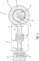
- FIG. 1 is a diagram illustrating a configuration of flex connector 40 for use in connecting multiple electronic systems.
- Flex connector 40 includes connector portions 42 and 44, middle portion 46 and spiral portion 48.
- Connector portion 42 includes topside connectors 50 and connector portion 44 includes underside connectors 52.
- Middle portion 46 includes bend points 54 and 56, connector portion 58 and curved portion 60.
- Spiral portion 48 includes circumferential portion 62 and curved portion 64.
- Connector portion 58 includes underside connectors 66. While illustrated in FIG. 1 as topside connectors 50 and underside connectors 52 and 66, connectors 50, 52 and 66 may be implemented on either surface of connector portions 42, 44 and 58 depending on the configuration of the electronic systems for which flex connector 40 is connecting.
- Bend points 54 and 56 are designated points on middle portion 46 for which flex connector 40 will bend while in an operational state.
- a device may have circuit boards that are parallel to one another while the device is in the operational state.
- bend points 54 and 56 are the designated points of flex connector 40 that will provide a 90° gradual bend, for example, to facilitate connection of connectors 50 and 52 to the circuit boards.
- Bend points 54 and 56 are the only points of flex connector 40 that are bent during an operational state of the device. This reduces the overall stress placed upon flex connector 40 while the device is operational.
- Middle portion 46 may also include connector portion 58 to allow connection, for example, to external systems or other subsystems of a device.
- the device may include an external port within its housing to allow for connection to connectors 66. This may facilitate, for example, connection to the electronic systems of the device without the need to open the device. This way, diagnostics may easily be run on the device while the device remains in an operational state.
- connectors 66 may be implemented to connect to further electronic subsystems of a device, providing more efficient use of the internal spaces of the device.
- Spiral portion 48 allows connector portions 44 and 46 to move apart and away from one another without causing any undue stress on flex connector 40.
- Curved portion 60 connects bend point 56 to circumferential portion 62.
- Curved portion 60 includes a turn that transitions the lateral direction of middle portion 46 into the circular direction of circumferential portion 62.
- Circumferential portion 62 extends around connector portion 44.
- Circumferential portion 62 may complete a 360° revolution around connector portion 44, as is illustrated in the embodiment shown in FIG. 1 .
- circumferential portion 62 may extend greater than or less than 360° around connector portion 44, depending upon the desired distance connector portions 42 and 44 may be pulled apart from one another without creating any undue stress upon flex connector 40 or any other components of the device.
- circumferential portion 62 is configured in a common plane with connector portion 44.
- Flex connector 40 may be implemented as any type of flexible electronics, for example, such as electronic circuits mounted on flexible plastic substrates.
- Connector portions 42, 44 and 58 of flex connector 40 may be implemented as either flexible electronics, or as rigid printed circuit boards, for example.
- Flex connector 40 may include only electrical interconnections between connectors 42, 44 and 58, or may include other electronic circuit components, for example. To accommodate a greater number of electrical interconnections, flex connector 40 may include more than one layer. For example, several flex connectors 40 may be connected to common connectors 42, 44 and 58 to provide a greater number of electrical interconnections between connectors 42, 44 and 58.
- FIG. 2 is a diagram illustrating device 200 in an operational state that includes circuit boards 202 and 204 connected by flex connector 40.
- Device 200 may include compartments 206 and 208.
- Circuit board 202 may be positioned within compartment 206 and circuit board 204 may be positioned within compartment 208.
- Device 200 is any device in which electronic circuits must connect to one another such as, for example, airborne munitions.
- Connectors 50 may be connected to circuit board 202 and connector 52 may be connected to circuit board 204.
- connector portions 42 and 44 are substantially parallel to one another based upon the parallel configuration of circuit boards 202 and 204.
- Middle portion 46 extends along an inside surface of device 200 across both compartments 206 and 208. While illustrated as connecting to circuit board 202 utilizing topside connectors, connector portion 42 may be configured to connect to either side of circuit board 202.
- Bend point 54 bends gradually around circuit board 202 through an opening between circuit board 202 and an inside surface of compartment 206. While illustrated as connecting to circuit board 204 using underside connectors, connector portion 44 may be configured to connect to either side of circuit board 204.
- Middle portion 46 may be perpendicular to circuit boards 202 and 204 and may run along an inside surface of device 200. Because spiral portion 48 exists in the same plane as connector portion 44, flex connector 40 takes up minimal space within device 200 while device 200 is in an operational state. Additionally, in high stress environments, such as that of an airborne munition, spiral portion 48 being in the same plane as connector portion 44 minimizes the stress placed on flex connector 40 due to g-forces experienced by device 200. In prior art systems, electrical connectors between circuit boards 202 and 204 were folded back and forth upon themselves during operational states of device 200. These folds can cause unwanted stress for the electrical connector, which can be exacerbated in high g-force environments. By utilizing flex connector 40, stresses experienced by the electrical connectors can be minimized.
- a physical channel may also be implemented within compartments 206 and 208 through which middle portion 46 may run. This would separate flex connector 40 from other internal components, further reducing the stress placed upon flex connector 40 during operation of device 200.
- connector portion 58 Another advantage of utilizing flex connector 40 is connector portion 58.
- An access port (not shown) may be included in compartment 206 to allow access to connector 66. This may allow, for example, external systems, separate from circuit boards 202 and 204, such as diagnostic systems to connect to the internal electronics of device 200 without the need of disassembling device 200.
- another circuit board may be implemented within compartment 206 to which connector portion 58 connects.
- FIG. 3 is a diagram illustrating device 200 in a disassembled state.
- compartments 206 and 208 are detached at 90°, with flex connector 40 continuing to connect circuit boards 202 and 204. This provides ease of access to internal components while performing maintenance, for example, without the need for disconnection of circuit boards 202 and 204 and without undue stress placed upon flex connector 40.
- spiral portion 48 allows connector portions 42 and 44 to pull apart and away from one another.
- circumferential portion 62 is pulled out of the common plane and away from connector portion 44. Because circumferential portion 62 is substantially circular and gradually bends around connector portion 44, circumferential portion 62 may be pulled outward toward middle portion 46 without experiencing high amounts of stress. As illustrated in FIG. 3 , this allows compartments 206 and 208 to be fully disconnected and pulled apart at a full 90° or greater.
- a flexible circuit connector for connecting first and second circuit boards of a device includes a first connector, a second connector and a spiral portion.
- the first connector is configured to connect to the first circuit board and the second connector is configured to connect to the second circuit board.
- the spiral portion is connected between the first and second connectors and includes a circumferential portion that extends around the second connector.
- the flexible circuit connector of the preceding paragraph can optionally include, additionally and/or alternatively, any one or more of the following features, configurations, operations, and/or additional components:
- a further embodiment of the foregoing connector may further include a middle portion connected between the first connector and the spiral portion, wherein the middle portion is connected to the first connector at a first bend point, and wherein the middle portion is connected to the spiral portion at a second bend point, and wherein the flexible circuit connector only bends at the first and second bend points when the device is in an operational state.
- first and second bend points are configured such that the first and second connectors are parallel to one another in the operational state.
- the spiral portion and the second connector are configured in a common plane during the operational state.
- the common plane is configured perpendicular to the middle portion during the operational state.
- the middle portion incudes a third connector configured to connect to an electronic system separate from the first and second circuit boards.
- the circumferential portion extends 360° around the second connector.
- the spiral portion is configured to pull out of the common plane toward the first connector when the first and second connectors are pulled apart from one another.
- An electronic system includes first and second circuit boards and a flexible circuit connector.
- the flexible circuit connector is configured to electrically connect the first and second circuit boards.
- the flexible circuit connector includes first and second connectors and a spiral portion.
- the first connector is configured to connect to the first circuit board.
- the second connector is configured to connect to the second circuit board.
- the spiral portion is connected between the first and second circuit boards and includes a circumferential portion that extends around the second connector.
- the electronic system of the preceding paragraph can optionally include, additionally and/or alternatively, any one or more of the following features, configurations, operations, and/or additional components:
- the flexible circuit connector further includes a middle portion connected between the first connector and the spiral portion, wherein the middle portion is connected to the first connector at a first bend point, and wherein the middle portion is connected to the spiral portion at a second bend point.
- the flexible circuit connector only bends at the first and second bend points when the device is in an operational state.
- first and second circuit boards are parallel to one another in the operational state, and wherein the first and second bend points are configured such that the first and second connectors are parallel to one another in the operational state.
- the spiral portion and the second connector are configured in a common plane during the operational state.
- the common plane is configured perpendicular to the middle portion during the operational state.
- the middle portion incudes a third connector configured to connect to an electronic circuit separate from the first and second circuit boards.
- the electronic system is contained within an airborne munition.
- the airborne munition includes first and second compartments, and wherein the first compartment is detachable from the second compartment, and wherein the first circuit board is positioned within the first compartment, and wherein the second circuit board is positioned within the second compartment.
- the spiral portion is configured to pull out of the common plane when the first and second compartments are detached and pulled apart from one another.
- the operational state comprises the first compartment and the second compartment attached to one another.
Landscapes
- Engineering & Computer Science (AREA)
- Microelectronics & Electronic Packaging (AREA)
- General Engineering & Computer Science (AREA)
- Manufacturing & Machinery (AREA)
- Coupling Device And Connection With Printed Circuit (AREA)
- Combinations Of Printed Boards (AREA)
Applications Claiming Priority (1)
| Application Number | Priority Date | Filing Date | Title |
|---|---|---|---|
| US15/071,745 US10109939B2 (en) | 2016-03-16 | 2016-03-16 | Flex circuit connector configuration |
Publications (2)
| Publication Number | Publication Date |
|---|---|
| EP3220096A1 true EP3220096A1 (de) | 2017-09-20 |
| EP3220096B1 EP3220096B1 (de) | 2021-06-30 |
Family
ID=58461058
Family Applications (1)
| Application Number | Title | Priority Date | Filing Date |
|---|---|---|---|
| EP17161125.4A Active EP3220096B1 (de) | 2016-03-16 | 2017-03-15 | Elektronikanordnung mit verbinderkonfiguration in form einer flexible schaltung |
Country Status (2)
| Country | Link |
|---|---|
| US (1) | US10109939B2 (de) |
| EP (1) | EP3220096B1 (de) |
Cited By (1)
| Publication number | Priority date | Publication date | Assignee | Title |
|---|---|---|---|---|
| WO2020182522A1 (de) * | 2019-03-08 | 2020-09-17 | Thyssenkrupp Ag | Steuergerät für ein lenksystem eines kraftfahrzeugs, elektromechanische kraftfahrzeugservolenkung und steer-by-wire lenksystem |
Citations (4)
| Publication number | Priority date | Publication date | Assignee | Title |
|---|---|---|---|---|
| US6287021B1 (en) * | 1998-05-20 | 2001-09-11 | Nikon Corporation | Apparatus for coupling electronic components within electronic devices such as cameras |
| US20040154824A1 (en) * | 2002-11-26 | 2004-08-12 | Hesse & Knipps Gmbh | Contact assembly for a rotatable circuit element |
| US20060176677A1 (en) * | 2003-08-27 | 2006-08-10 | Visteon Global Technologies, Inc. | Assembly comprising multiple microelectronic modules |
| US20120242364A1 (en) * | 2011-03-25 | 2012-09-27 | Vega Grieshaber Kg | Flexible connecting cable for electrically connecting a transducer and a transmitter of a measurement module |
Family Cites Families (13)
| Publication number | Priority date | Publication date | Assignee | Title |
|---|---|---|---|---|
| US4264115A (en) | 1978-03-01 | 1981-04-28 | Bunker Ramo Corporation | Interstage electrical connector |
| US4509109A (en) * | 1982-09-13 | 1985-04-02 | Hansen Thomas C | Electronically controlled coil assembly |
| JP2790056B2 (ja) * | 1994-02-04 | 1998-08-27 | 株式会社デンソー | 可撓性プリント配線板とその製造方法 |
| JP2002368440A (ja) * | 2001-06-06 | 2002-12-20 | Toshiba Corp | 折り畳み型電子機器とそのフレキシブル基板 |
| US6744637B2 (en) | 2001-11-30 | 2004-06-01 | Alliant Techsystems Inc. | Guided munitions electronics package and method |
| US6778389B1 (en) * | 2003-07-03 | 2004-08-17 | Visteon Global Technologies, Inc. | Microelectronic package with tubular housing |
| US7531752B2 (en) * | 2003-07-24 | 2009-05-12 | Nec Corporation | Flexible substrate and electronic device |
| DE102004018009B3 (de) | 2004-04-14 | 2005-10-13 | Knorr-Bremse Systeme für Schienenfahrzeuge GmbH | Magnetschienenbremsvorrichtung |
| JP2008187154A (ja) * | 2007-01-31 | 2008-08-14 | Nitto Denko Corp | フレキシブル配線回路基板の接続構造および電子機器 |
| US8043115B2 (en) * | 2008-12-19 | 2011-10-25 | Nokia Corporation | Apparatus and methods |
| US8559191B2 (en) | 2009-01-05 | 2013-10-15 | Raytheon Company | Multi-purpose mounting devices for mounting electrical packages to airborne objects |
| US8635937B2 (en) | 2010-09-03 | 2014-01-28 | Raytheon Company | Systems and methods for launching munitions |
| US10184763B2 (en) | 2014-02-11 | 2019-01-22 | Raytheon Company | Munition with nose kit connecting to aft casing connector |
-
2016
- 2016-03-16 US US15/071,745 patent/US10109939B2/en active Active
-
2017
- 2017-03-15 EP EP17161125.4A patent/EP3220096B1/de active Active
Patent Citations (4)
| Publication number | Priority date | Publication date | Assignee | Title |
|---|---|---|---|---|
| US6287021B1 (en) * | 1998-05-20 | 2001-09-11 | Nikon Corporation | Apparatus for coupling electronic components within electronic devices such as cameras |
| US20040154824A1 (en) * | 2002-11-26 | 2004-08-12 | Hesse & Knipps Gmbh | Contact assembly for a rotatable circuit element |
| US20060176677A1 (en) * | 2003-08-27 | 2006-08-10 | Visteon Global Technologies, Inc. | Assembly comprising multiple microelectronic modules |
| US20120242364A1 (en) * | 2011-03-25 | 2012-09-27 | Vega Grieshaber Kg | Flexible connecting cable for electrically connecting a transducer and a transmitter of a measurement module |
Cited By (1)
| Publication number | Priority date | Publication date | Assignee | Title |
|---|---|---|---|---|
| WO2020182522A1 (de) * | 2019-03-08 | 2020-09-17 | Thyssenkrupp Ag | Steuergerät für ein lenksystem eines kraftfahrzeugs, elektromechanische kraftfahrzeugservolenkung und steer-by-wire lenksystem |
Also Published As
| Publication number | Publication date |
|---|---|
| EP3220096B1 (de) | 2021-06-30 |
| US10109939B2 (en) | 2018-10-23 |
| US20170271792A1 (en) | 2017-09-21 |
Similar Documents
| Publication | Publication Date | Title |
|---|---|---|
| EP3220484B1 (de) | Verbinderkonfiguration für flexible schaltung | |
| US20150360627A1 (en) | Wire harness | |
| EP1995823A3 (de) | Kommunikationsrelais-Vorrichtung und Relais-Anschlusseinheit | |
| EP3018983A2 (de) | Elektronische vorrichtung | |
| EP3133701B1 (de) | Integrierter eingangs-/ausgangsverbinder | |
| EP3220096B1 (de) | Elektronikanordnung mit verbinderkonfiguration in form einer flexible schaltung | |
| EP2306592A2 (de) | Vorrichtung zum Anschließen eines Kabels mit mehreren Leitern an einen Steckverbinder Stiftgitteranordnung | |
| US9368922B2 (en) | Connector | |
| CN112009202B (zh) | 加热装置 | |
| WO2004075348A2 (en) | Three-way connector | |
| CN107845868B (zh) | 具有增大的安装表面的电动汽车连接器 | |
| WO2012091998A2 (en) | Serial transmission system and slave unit used therein | |
| US10424986B2 (en) | Actuator | |
| CN109313480B (zh) | 控制系统 | |
| US20160294117A1 (en) | Electrical Connector System With Laterally Protruding Releasing Arm | |
| CN103577370B (zh) | 复式连接器互连系统 | |
| US20200251888A1 (en) | Wiring structure | |
| US9325108B2 (en) | Electrical connector assembly for an electronic module | |
| EP3030056B1 (de) | Vorrichtung zur bildung einer abgerundeten biegung in einem flachen flexiblen kabel | |
| US20200225717A1 (en) | Modular controllers | |
| JPH06275925A (ja) | 電子回路基板 | |
| EP3701593B1 (de) | Anordnung mit einem elektrischer anschluss mit einer käfigklemme für drahtabschluss | |
| EP2509401A2 (de) | Mikroelektronische Anwendungen | |
| CN106020373B (zh) | 计算机、服务器、模块、连接器组、装配方法和控制方法 | |
| CN108141974B (zh) | 电路板组件 |
Legal Events
| Date | Code | Title | Description |
|---|---|---|---|
| PUAI | Public reference made under article 153(3) epc to a published international application that has entered the european phase |
Free format text: ORIGINAL CODE: 0009012 |
|
| STAA | Information on the status of an ep patent application or granted ep patent |
Free format text: STATUS: THE APPLICATION HAS BEEN PUBLISHED |
|
| AK | Designated contracting states |
Kind code of ref document: A1 Designated state(s): AL AT BE BG CH CY CZ DE DK EE ES FI FR GB GR HR HU IE IS IT LI LT LU LV MC MK MT NL NO PL PT RO RS SE SI SK SM TR |
|
| AX | Request for extension of the european patent |
Extension state: BA ME |
|
| STAA | Information on the status of an ep patent application or granted ep patent |
Free format text: STATUS: REQUEST FOR EXAMINATION WAS MADE |
|
| 17P | Request for examination filed |
Effective date: 20180319 |
|
| RBV | Designated contracting states (corrected) |
Designated state(s): AL AT BE BG CH CY CZ DE DK EE ES FI FR GB GR HR HU IE IS IT LI LT LU LV MC MK MT NL NO PL PT RO RS SE SI SK SM TR |
|
| STAA | Information on the status of an ep patent application or granted ep patent |
Free format text: STATUS: EXAMINATION IS IN PROGRESS |
|
| 17Q | First examination report despatched |
Effective date: 20201027 |
|
| GRAP | Despatch of communication of intention to grant a patent |
Free format text: ORIGINAL CODE: EPIDOSNIGR1 |
|
| STAA | Information on the status of an ep patent application or granted ep patent |
Free format text: STATUS: GRANT OF PATENT IS INTENDED |
|
| INTG | Intention to grant announced |
Effective date: 20210127 |
|
| GRAS | Grant fee paid |
Free format text: ORIGINAL CODE: EPIDOSNIGR3 |
|
| GRAA | (expected) grant |
Free format text: ORIGINAL CODE: 0009210 |
|
| STAA | Information on the status of an ep patent application or granted ep patent |
Free format text: STATUS: THE PATENT HAS BEEN GRANTED |
|
| AK | Designated contracting states |
Kind code of ref document: B1 Designated state(s): AL AT BE BG CH CY CZ DE DK EE ES FI FR GB GR HR HU IE IS IT LI LT LU LV MC MK MT NL NO PL PT RO RS SE SI SK SM TR |
|
| REG | Reference to a national code |
Ref country code: CH Ref legal event code: EP |
|
| REG | Reference to a national code |
Ref country code: DE Ref legal event code: R096 Ref document number: 602017041086 Country of ref document: DE Ref country code: AT Ref legal event code: REF Ref document number: 1406724 Country of ref document: AT Kind code of ref document: T Effective date: 20210715 |
|
| REG | Reference to a national code |
Ref country code: IE Ref legal event code: FG4D |
|
| REG | Reference to a national code |
Ref country code: LT Ref legal event code: MG9D |
|
| PG25 | Lapsed in a contracting state [announced via postgrant information from national office to epo] |
Ref country code: HR Free format text: LAPSE BECAUSE OF FAILURE TO SUBMIT A TRANSLATION OF THE DESCRIPTION OR TO PAY THE FEE WITHIN THE PRESCRIBED TIME-LIMIT Effective date: 20210630 Ref country code: BG Free format text: LAPSE BECAUSE OF FAILURE TO SUBMIT A TRANSLATION OF THE DESCRIPTION OR TO PAY THE FEE WITHIN THE PRESCRIBED TIME-LIMIT Effective date: 20210930 Ref country code: FI Free format text: LAPSE BECAUSE OF FAILURE TO SUBMIT A TRANSLATION OF THE DESCRIPTION OR TO PAY THE FEE WITHIN THE PRESCRIBED TIME-LIMIT Effective date: 20210630 |
|
| REG | Reference to a national code |
Ref country code: NL Ref legal event code: MP Effective date: 20210630 |
|
| REG | Reference to a national code |
Ref country code: AT Ref legal event code: MK05 Ref document number: 1406724 Country of ref document: AT Kind code of ref document: T Effective date: 20210630 |
|
| PG25 | Lapsed in a contracting state [announced via postgrant information from national office to epo] |
Ref country code: LV Free format text: LAPSE BECAUSE OF FAILURE TO SUBMIT A TRANSLATION OF THE DESCRIPTION OR TO PAY THE FEE WITHIN THE PRESCRIBED TIME-LIMIT Effective date: 20210630 Ref country code: GR Free format text: LAPSE BECAUSE OF FAILURE TO SUBMIT A TRANSLATION OF THE DESCRIPTION OR TO PAY THE FEE WITHIN THE PRESCRIBED TIME-LIMIT Effective date: 20211001 Ref country code: NO Free format text: LAPSE BECAUSE OF FAILURE TO SUBMIT A TRANSLATION OF THE DESCRIPTION OR TO PAY THE FEE WITHIN THE PRESCRIBED TIME-LIMIT Effective date: 20210930 Ref country code: RS Free format text: LAPSE BECAUSE OF FAILURE TO SUBMIT A TRANSLATION OF THE DESCRIPTION OR TO PAY THE FEE WITHIN THE PRESCRIBED TIME-LIMIT Effective date: 20210630 Ref country code: SE Free format text: LAPSE BECAUSE OF FAILURE TO SUBMIT A TRANSLATION OF THE DESCRIPTION OR TO PAY THE FEE WITHIN THE PRESCRIBED TIME-LIMIT Effective date: 20210630 |
|
| PG25 | Lapsed in a contracting state [announced via postgrant information from national office to epo] |
Ref country code: SK Free format text: LAPSE BECAUSE OF FAILURE TO SUBMIT A TRANSLATION OF THE DESCRIPTION OR TO PAY THE FEE WITHIN THE PRESCRIBED TIME-LIMIT Effective date: 20210630 Ref country code: SM Free format text: LAPSE BECAUSE OF FAILURE TO SUBMIT A TRANSLATION OF THE DESCRIPTION OR TO PAY THE FEE WITHIN THE PRESCRIBED TIME-LIMIT Effective date: 20210630 Ref country code: AT Free format text: LAPSE BECAUSE OF FAILURE TO SUBMIT A TRANSLATION OF THE DESCRIPTION OR TO PAY THE FEE WITHIN THE PRESCRIBED TIME-LIMIT Effective date: 20210630 Ref country code: EE Free format text: LAPSE BECAUSE OF FAILURE TO SUBMIT A TRANSLATION OF THE DESCRIPTION OR TO PAY THE FEE WITHIN THE PRESCRIBED TIME-LIMIT Effective date: 20210630 Ref country code: CZ Free format text: LAPSE BECAUSE OF FAILURE TO SUBMIT A TRANSLATION OF THE DESCRIPTION OR TO PAY THE FEE WITHIN THE PRESCRIBED TIME-LIMIT Effective date: 20210630 Ref country code: NL Free format text: LAPSE BECAUSE OF FAILURE TO SUBMIT A TRANSLATION OF THE DESCRIPTION OR TO PAY THE FEE WITHIN THE PRESCRIBED TIME-LIMIT Effective date: 20210630 Ref country code: PT Free format text: LAPSE BECAUSE OF FAILURE TO SUBMIT A TRANSLATION OF THE DESCRIPTION OR TO PAY THE FEE WITHIN THE PRESCRIBED TIME-LIMIT Effective date: 20211102 Ref country code: RO Free format text: LAPSE BECAUSE OF FAILURE TO SUBMIT A TRANSLATION OF THE DESCRIPTION OR TO PAY THE FEE WITHIN THE PRESCRIBED TIME-LIMIT Effective date: 20210630 Ref country code: ES Free format text: LAPSE BECAUSE OF FAILURE TO SUBMIT A TRANSLATION OF THE DESCRIPTION OR TO PAY THE FEE WITHIN THE PRESCRIBED TIME-LIMIT Effective date: 20210630 |
|
| PG25 | Lapsed in a contracting state [announced via postgrant information from national office to epo] |
Ref country code: PL Free format text: LAPSE BECAUSE OF FAILURE TO SUBMIT A TRANSLATION OF THE DESCRIPTION OR TO PAY THE FEE WITHIN THE PRESCRIBED TIME-LIMIT Effective date: 20210630 |
|
| REG | Reference to a national code |
Ref country code: DE Ref legal event code: R097 Ref document number: 602017041086 Country of ref document: DE |
|
| PG25 | Lapsed in a contracting state [announced via postgrant information from national office to epo] |
Ref country code: DK Free format text: LAPSE BECAUSE OF FAILURE TO SUBMIT A TRANSLATION OF THE DESCRIPTION OR TO PAY THE FEE WITHIN THE PRESCRIBED TIME-LIMIT Effective date: 20210630 |
|
| PLBE | No opposition filed within time limit |
Free format text: ORIGINAL CODE: 0009261 |
|
| STAA | Information on the status of an ep patent application or granted ep patent |
Free format text: STATUS: NO OPPOSITION FILED WITHIN TIME LIMIT |
|
| PG25 | Lapsed in a contracting state [announced via postgrant information from national office to epo] |
Ref country code: AL Free format text: LAPSE BECAUSE OF FAILURE TO SUBMIT A TRANSLATION OF THE DESCRIPTION OR TO PAY THE FEE WITHIN THE PRESCRIBED TIME-LIMIT Effective date: 20210630 |
|
| 26N | No opposition filed |
Effective date: 20220331 |
|
| PG25 | Lapsed in a contracting state [announced via postgrant information from national office to epo] |
Ref country code: IT Free format text: LAPSE BECAUSE OF FAILURE TO SUBMIT A TRANSLATION OF THE DESCRIPTION OR TO PAY THE FEE WITHIN THE PRESCRIBED TIME-LIMIT Effective date: 20210630 |
|
| PG25 | Lapsed in a contracting state [announced via postgrant information from national office to epo] |
Ref country code: MC Free format text: LAPSE BECAUSE OF FAILURE TO SUBMIT A TRANSLATION OF THE DESCRIPTION OR TO PAY THE FEE WITHIN THE PRESCRIBED TIME-LIMIT Effective date: 20210630 |
|
| REG | Reference to a national code |
Ref country code: CH Ref legal event code: PL |
|
| REG | Reference to a national code |
Ref country code: BE Ref legal event code: MM Effective date: 20220331 |
|
| PG25 | Lapsed in a contracting state [announced via postgrant information from national office to epo] |
Ref country code: LU Free format text: LAPSE BECAUSE OF NON-PAYMENT OF DUE FEES Effective date: 20220315 Ref country code: LI Free format text: LAPSE BECAUSE OF NON-PAYMENT OF DUE FEES Effective date: 20220331 Ref country code: IE Free format text: LAPSE BECAUSE OF NON-PAYMENT OF DUE FEES Effective date: 20220315 Ref country code: CH Free format text: LAPSE BECAUSE OF NON-PAYMENT OF DUE FEES Effective date: 20220331 |
|
| PG25 | Lapsed in a contracting state [announced via postgrant information from national office to epo] |
Ref country code: BE Free format text: LAPSE BECAUSE OF NON-PAYMENT OF DUE FEES Effective date: 20220331 |
|
| PG25 | Lapsed in a contracting state [announced via postgrant information from national office to epo] |
Ref country code: LT Free format text: LAPSE BECAUSE OF FAILURE TO SUBMIT A TRANSLATION OF THE DESCRIPTION OR TO PAY THE FEE WITHIN THE PRESCRIBED TIME-LIMIT Effective date: 20210630 |
|
| PG25 | Lapsed in a contracting state [announced via postgrant information from national office to epo] |
Ref country code: HU Free format text: LAPSE BECAUSE OF FAILURE TO SUBMIT A TRANSLATION OF THE DESCRIPTION OR TO PAY THE FEE WITHIN THE PRESCRIBED TIME-LIMIT; INVALID AB INITIO Effective date: 20170315 |
|
| PG25 | Lapsed in a contracting state [announced via postgrant information from national office to epo] |
Ref country code: MK Free format text: LAPSE BECAUSE OF FAILURE TO SUBMIT A TRANSLATION OF THE DESCRIPTION OR TO PAY THE FEE WITHIN THE PRESCRIBED TIME-LIMIT Effective date: 20210630 Ref country code: CY Free format text: LAPSE BECAUSE OF FAILURE TO SUBMIT A TRANSLATION OF THE DESCRIPTION OR TO PAY THE FEE WITHIN THE PRESCRIBED TIME-LIMIT Effective date: 20210630 |
|
| PG25 | Lapsed in a contracting state [announced via postgrant information from national office to epo] |
Ref country code: MT Free format text: LAPSE BECAUSE OF FAILURE TO SUBMIT A TRANSLATION OF THE DESCRIPTION OR TO PAY THE FEE WITHIN THE PRESCRIBED TIME-LIMIT Effective date: 20210630 |
|
| REG | Reference to a national code |
Ref country code: DE Ref legal event code: R081 Ref document number: 602017041086 Country of ref document: DE Owner name: SIMMONDS PRECISION PRODUCTS, INC., VERGENNES, US Free format text: FORMER OWNER: ROSEMOUNT AEROSPACE INC., BURNSVILLE, MN, US |
|
| REG | Reference to a national code |
Ref country code: GB Ref legal event code: 732E Free format text: REGISTERED BETWEEN 20250911 AND 20250917 |
|
| PG25 | Lapsed in a contracting state [announced via postgrant information from national office to epo] |
Ref country code: TR Free format text: LAPSE BECAUSE OF FAILURE TO SUBMIT A TRANSLATION OF THE DESCRIPTION OR TO PAY THE FEE WITHIN THE PRESCRIBED TIME-LIMIT Effective date: 20210630 |
|
| PGFP | Annual fee paid to national office [announced via postgrant information from national office to epo] |
Ref country code: GB Payment date: 20260325 Year of fee payment: 10 |
|
| PGFP | Annual fee paid to national office [announced via postgrant information from national office to epo] |
Ref country code: DE Payment date: 20260317 Year of fee payment: 10 |
|
| PGFP | Annual fee paid to national office [announced via postgrant information from national office to epo] |
Ref country code: FR Payment date: 20260323 Year of fee payment: 10 |